

Page 1

R
RocketIO™ X
Transceiver
User Guide
UG035 (v1.5) November 22, 2004
Page 2

RocketIO™ X Transceiver User Guide www.xilinx.com UG035 (v1.5) November 22, 2004
1-800-255-7778
“Xilinx” and the Xilinx logo shown above are registered trademarks of Xilinx, Inc. Any rights not expressly granted herein are reserved.
CoolRunner, RocketChips, Rocket IP, Spartan, StateBENCH, StateCAD, Virtex, XACT, XC2064, XC3090, XC4005, and XC5210 are
registered trademarks of Xilinx, Inc.
The shadow X shown above is a trademark of Xilinx, Inc.
ACE Controller, ACE Flash, A.K.A. Speed, Alliance Series, AllianceCORE, Bencher, ChipScope, Configurable Logic Cell, CORE Generator,
CoreLINX, Dual Block, EZTag, Fast CLK, Fast CONNECT, Fast FLASH, FastMap, Fast Zero Power, Foundation, Gigabit Speeds...and
Beyond!, HardWire, HDL Bencher, IRL, J Drive, JBits, LCA, LogiBLOX, Logic Cell, LogiCORE, LogicProfessor, MicroBlaze, MicroVia,
MultiLINX, NanoBlaze, PicoBlaze, PLUSASM, PowerGuide, PowerMaze, QPro, Real-PCI, RocketIO, SelectIO, SelectRAM, SelectRAM+,
Silicon Xpresso, Smartguide, Smart-IP, SmartSearch, SMARTswitch, System ACE, Testbench In A Minute, TrueMap, UIM, VectorMaze,
VersaBlock, VersaRing, Virtex-II Pro, Virtex-II EasyPath, Wave Table, WebFITTER, WebPACK, WebPOWERED, XABEL, XACTFloorplanner, XACT-Performance, XACTstep Advanced, XACTstep Foundry, XAM, XAPP, X-BLOX +, XC designated products, XChecker,
XDM, XEPLD, Xilinx Foundation Series, Xilinx XDTV, Xinfo, XSI, XtremeDSP and ZERO+ are trademarks of Xilinx, Inc.
The Programmable Logic Company is a service mark of Xilinx, Inc.
All other trademarks are the proper ty of their respective owners.
Xilinx, Inc. does not assume any liability arising out of the application or use of any product described or shown herein; nor does it convey
any license under its patents, copyrights, or maskwork rights or any rights of others. Xilinx, Inc. reserves the right to make changes, at any
time, in order to improve reliability, function or design and to supply the best product possible. Xilinx, Inc. will not assume responsibility for
the use of any circuitry described herein other than circuitry entirely embodied in its products. Xilinx provides any design, code, or
information shown or described herein “as is.” By providing the design, code, or information as one possible implementation of a feature,
application, or standard, Xilinx makes no representation that such implementation is free from any claims of infringement. You are
responsible for obtaining any rights you may require for your implementation. Xilinx expressly disclaims any warranty whatsoever with
respect to the adequacy of any such implementation, including but not limited to any warranties or representations that the implementation
is free from claims of infringement, as well as any implied warranties of merchantability or fitness for a particular purpose. Xilinx, Inc. devices
and products are protected under U.S. Patents. Other U.S. and foreign patents pending. Xilinx, Inc. does not represent that devices shown
or products described herein are free from patent infringement or from any other third par ty right. Xilinx, Inc. assumes no obligation to
correct any errors contained herein or to advise any user of this text of any correction if such be made. Xilinx, Inc. will not assume any liability
for the accuracy or correctness of any engineering or software support or assistance provided to a user.
Xilinx products are not intended for use in life support appliances, devices, or systems. Use of a Xilinx product in such applications without
the written consent of the appropriate Xilinx officer is prohibited.
The contents of this manual are owned and copyrighted by Xilinx. Copyright 1994-2003 Xilinx, Inc. All Rights Reserved. Except as stated
herein, none of the material may be copied, reproduced, distributed, republished, downloaded, displayed, posted, or transmitted in any form
or by any means including, but not limited to, electronic, mechanical, photocopying, recording, or otherwise, without the prior written consent
of Xilinx. Any unauthorized use of any material contained in this manual may violate copyright laws, trademark laws, the laws of privacy and
publicity, and communications regulations and statutes.
RocketIO™ X Transceiver User Guide
UG035 (v1.5) November 22, 2004
The following table shows the revision history for this document.
R
Date Version Revision
10/31/03 1.0 Xilinx initial release. (ADVANCE DRAFT)
11/14/03 1.1 Minor updates made throughout.
12/09/03 1.2 Additions to end of Chapter 2 and minor changes Appendix C.
12/16/03 1.2.1 Change made to “Status Indication.”
Page 3

UG035 (v1.5) November 22, 2004 www.xilinx.com RocketIO™ X Transceiver User Guide
1-800-255-7778
03/09/04 1.3
Chapter 1, “RocketIO X Transceiver Overview”:
• Modified GT10 Primitive in “Definitions:,” page 25.
• Modified Tabl e 1-2 , pa ge 27 and added Note 3.
• Updated definitions in Primitive Ports, Tab l e 1- 4, pag e 2 8 . Made changes to:
BREFCLKNIN, BREFCLKPIN, PMAREGADDR[5:0], PMAREGDATAIN[7:0],
PMAREGRW, RXBUFSTATUS[1:0], RXCHARISCOMMA, RXCHARISK[7:0],
RXCLKCORCNT[2:0], RXCOMMADETUSE, RXDATA[63:0], RXDATAWIDTH[1:0],
RXDEC8B10BUSE, RXDESCRAM64B66BUSE, RXINTDATAWIDTH[1:0],
RXLOSSOFSYNC[1:0], RXNOTINTABLE[7:0], RXRUNDISP[7:0], RXUSRCLK,
RXUSRCLK2, TXBYPASS8B10B[7:0], TXCHARDISPMODE[7:0],
TXCHARDISPVAL[7:0], TXCHARISK[7:0], TXDATA[63:0], TXDATAWIDTH[1:0],
TXGEARBOX64B66BUSE, TXINTDATAWIDTH[1:0], TXKERR[7:0], TXRUNDISP[7:0],
TXSCRAM64B66BUSE, TXUSRCLK, and TXUSRCLK2.
• Updated RocketIO X Transceiver Attributes, Tab l e 1-5, pa ge 35. Made changes to:
ALIGN_COMMA_WORD, CHAN_BOND_MODE, CHAN_BOND_SEQ_1_*[10:0],
CLK_COR_8B10B_DE, CLK_COR_MAX_LAT, CLK_COR_MIN_LAT,
CLK_COR_SEQ_2_USE, CLK_COR_SEQ_LEN, and RX_LOSS_OF_SYNC_FSM.
• Updated text under “Modifiable Attributes,” page 39 and created new Appendix F,
“Modifiable Attributes.”
Chapter 2, “Digital Design Considerations”
• Changed last sentence of the last paragraph under 8B/10B Tab l e , pa ge 48 .
• Added sentence to “RXNOTINTABLE,” page 51.
• Modified Tabl e 2-8 , pa ge 54 .
• Added new heading, “Setting MCOMMA_10B_VALUE, PCOMMA_10B_VALUE, and
COMMA_10B_MASK (Special Note),” page 54.
• Corrected column heading in Table 2-9 , page 55.
• Added small table to show byte alignment options under “ALIGN_COMMA_WORD,”
page 56.
• Modified text under 64B/66B Encoder “Bypassing,” page 57 and made changes to
Table 2-10, page 57.
• Added note to section, “Scrambler,” page 59 (Normal Operation).
• Updated “Functions Common to All Protocols” under section,“Clock Correction,”
page 63.
• Added text to “Clock Correction Sequences,” page 64 (relating to 11th bit format).
• Updated Attribute Setting column in Table 2-13, page 65.
• Added Channel Bonding match logic example under section “Channel Bonding,” page
65.
• Added new section, “Applications Without Channel Bonding.”
• Modified text under “Status Indication,” page 68 and changed Table 2-15, page 68.
• Modified text under “Event Indication,” page 69 and changed Table 2-17, page 69.
Chapter 3, “Clocking and Clock Domains”:
• Added note to “Clock Domain Architecture,” page 73.
• Modified Figure 3-1, page 73, Figure 3-2 and Figure 3-3. Minor editing change to Figure
3-4.
• Modified Figure 3-6 through Figure 3-12.
• Added new section, “PMA,” page 85 and Tab l e 3-3, pa g e 85 .
• Added new section, “Data Path Latency,” page 89, and new tables, Tab l e 3-4 , p a ge 89 ,
and Tab l e 3- 5, pag e 8 9 .
Date Version Revision
Page 4

RocketIO™ X Transceiver User Guide www.xilinx.com UG035 (v1.5) November 22, 2004
1-800-255-7778
03/09/04 1.3
(Continued)
Chapter 4, “Analog Design Considerations”:
• Modified text (at end of section) and added “LT1963A” to “Voltage Regulation,” page
114.
• Replaced Figure 4-23, page 117.
• Modified first paragraph under “Routing Serial Traces,” page 117.
• Modified Figure 4-31, page 122 and Figure 4-32, page 122.
• Deleted Figure 4-33.
• Chapter 5, “Simulation and Implementation”:
• Modified Tabl e 5-3 , pa ge 12 7 (Loopback Modes).
• Modified section, “Parallel Loopback,” page 128.
• Added new section, “Post/Pre-Driver Serial Loopback,” page 128.
Appendix B, “8B/10B Valid Characters:
• Updated Tab le B- 1, p age 1 37. Changed entries in “Current RD+” column for Data Byte
D9.1, D9.2, D9.3, D9.4, D9.5, D9.6, and D9.7.
Appendix C, “PMA Attribute Programming Bus:
• Added table references in “Register Definition” section and changed the order of the
register definitions.
• Modified Table C-1, page 147.
Appendix D, “Virtex-II Pro to Virtex-II Pro X FPGA Design Migration:
• Added note directly above Figure D-2, page 171.
• Added new section, “Migration Differences.”
Added new “Index.”
Date Version Revision
Page 5

UG035 (v1.5) November 22, 2004 www.xilinx.com RocketIO™ X Transceiver User Guide
1-800-255-7778
06/29/04 1.4 • Changed the PMA_SPEED attribute description in Tab le 1-5 .
• Modified “Clock Correction Sequences” in Chapter 2 and Tabl e 2- 13.
• Removed section, “Applications Without Channel Bonding” in Chapter 2.
• Modified first paragraph after Figure 2-6, page 50.
• Added illustration to section on “ALIGN_COMMA_WORD,” page 56.
• Added note to “Clock Correction Sequences,” page 64.
• Made change to Figure 2-12, page 67.
• Added sample Verilog code after Table 2-17, page 69.
• Added notes to Tab le 3-3, p a ge 85.
• Removed old Figure 3-2 through Figure 3-12 and related text. Replaced with new
Figure 3-2 through Figure 3-15 and related text.
• Added new section, “PMA” in Chapter 3 and modified Table 3- 3 , page 85.
• Chapter 3, “Clocking and Clock Domains” text revised; new Use Model figures and
Ta bl e 3- 2 added.
• Added note to “Simulation Transmitter Emphasis and Receiver Equalization
Settings,” page 112.
• Added “Conditions” to T
LOCK
row of Table 4-7, page 104.
• Updated Figure 4-32 and the paragraph above it.
• Removed sentence from the first paragraph of “Model Considerations” in Chapter 5.
• Added paragraph to “Post/Pre-Driver Serial Loopback” in Chapter 5 and modified
Ta bl e 5- 4.
• Made changes to Tab le A- 3, p age 1 3 4, Ta b le A-4, p a ge 135,and Tab le A-5, pa ge 136.
• Corrected Tab le B -1 .
• Added new Appendix G, “Related Online Documents.”
• Miscellaneous edits throughout.
11/22/04 1.5 • Changed RXCOMMADET definition in Ta bl e 1 -4 .
• Modified graphic illustrating “ALIGN_COMMA_WORD,” page 56.
• Added text to TXKERR[3] in Table 2-10, page 57 and a note to the table.
• Fixed error in Figure 3-10, page 79.
• Edited Mode Number column in Table 3- 3 , page 85 .
• Edited Tab le 4-6, p a ge 103 and added note.
• Changed VCSO number to EV-2101CA in text and in Figure 4-32, page 122.
• Added PMA attributes and updated Table C-2, page 148; added new PMA attribute
definitions.
• Added XAPP762 and XAPP767 to Appendix G, “Related Online Documents.”Also
added RPT007 to “Characterization Reports.”
Date Version Revision
Page 6

RocketIO™ X Transceiver User Guide www.xilinx.com UG035 (v1.5) November 22, 2004
1-800-255-7778
Page 7

UG035 (v1.5) November 22, 2004 www.xilinx.com RocketIO™ X Transceiver User Guide
1-800-255-7778
Contents
Preface: About This Guide
RocketIO X Features . . . . . . . . . . . . . . . . . . . . . . . . . . . . . . . . . . . . . . . . . . . . . . . . . . . . . . . . 21
User Guide Organization. . . . . . . . . . . . . . . . . . . . . . . . . . . . . . . . . . . . . . . . . . . . . . . . . . . . 21
Related Information. . . . . . . . . . . . . . . . . . . . . . . . . . . . . . . . . . . . . . . . . . . . . . . . . . . . . . . . . 22
Additional Resources . . . . . . . . . . . . . . . . . . . . . . . . . . . . . . . . . . . . . . . . . . . . . . . . . . . . . . . 22
User Guide Conventions . . . . . . . . . . . . . . . . . . . . . . . . . . . . . . . . . . . . . . . . . . . . . . . . . . . . 23
Port and Attribute Names. . . . . . . . . . . . . . . . . . . . . . . . . . . . . . . . . . . . . . . . . . . . . . . . . . 23
Comma Definition . . . . . . . . . . . . . . . . . . . . . . . . . . . . . . . . . . . . . . . . . . . . . . . . . . . . . . . . 23
Typographical. . . . . . . . . . . . . . . . . . . . . . . . . . . . . . . . . . . . . . . . . . . . . . . . . . . . . . . . . . . . 23
Chapter 1: RocketIO X Transceiver Overview
Basic Architecture and Capabilities. . . . . . . . . . . . . . . . . . . . . . . . . . . . . . . . . . . . . . . . . . 25
RocketIO X Transceiver Instantiations. . . . . . . . . . . . . . . . . . . . . . . . . . . . . . . . . . . . . . . 28
HDL Code Examples . . . . . . . . . . . . . . . . . . . . . . . . . . . . . . . . . . . . . . . . . . . . . . . . . . . . . . 28
Available Ports. . . . . . . . . . . . . . . . . . . . . . . . . . . . . . . . . . . . . . . . . . . . . . . . . . . . . . . . . . . . . . 28
Primitive Attributes . . . . . . . . . . . . . . . . . . . . . . . . . . . . . . . . . . . . . . . . . . . . . . . . . . . . . . . . . 35
Modifiable Attributes . . . . . . . . . . . . . . . . . . . . . . . . . . . . . . . . . . . . . . . . . . . . . . . . . . . . . . . 39
Byte Mapping. . . . . . . . . . . . . . . . . . . . . . . . . . . . . . . . . . . . . . . . . . . . . . . . . . . . . . . . . . . . . . . 39
Chapter 2: Digital Design Considerations
Top-Level Architecture. . . . . . . . . . . . . . . . . . . . . . . . . . . . . . . . . . . . . . . . . . . . . . . . . . . . . . 42
Transmit Architecture . . . . . . . . . . . . . . . . . . . . . . . . . . . . . . . . . . . . . . . . . . . . . . . . . . . . . 42
Receive Architecture . . . . . . . . . . . . . . . . . . . . . . . . . . . . . . . . . . . . . . . . . . . . . . . . . . . . . . 42
Operation Modes . . . . . . . . . . . . . . . . . . . . . . . . . . . . . . . . . . . . . . . . . . . . . . . . . . . . . . . . . 43
Block Level Functions . . . . . . . . . . . . . . . . . . . . . . . . . . . . . . . . . . . . . . . . . . . . . . . . . . . . . . . 43
Classification of Signals and Overloading . . . . . . . . . . . . . . . . . . . . . . . . . . . . . . . . . . . . 43
Static Signals (Control Inputs) . . . . . . . . . . . . . . . . . . . . . . . . . . . . . . . . . . . . . . . . . . . . 43
Dynamic Signals . . . . . . . . . . . . . . . . . . . . . . . . . . . . . . . . . . . . . . . . . . . . . . . . . . . . . . . 44
Bus Interface . . . . . . . . . . . . . . . . . . . . . . . . . . . . . . . . . . . . . . . . . . . . . . . . . . . . . . . . . . . . . 46
Selecting the External Configuration (Fabric Interface) . . . . . . . . . . . . . . . . . . . . . . . . . 46
Selecting the Internal Configuration . . . . . . . . . . . . . . . . . . . . . . . . . . . . . . . . . . . . . . . . 46
Clock Ratio . . . . . . . . . . . . . . . . . . . . . . . . . . . . . . . . . . . . . . . . . . . . . . . . . . . . . . . . . . . 46
8B/10B . . . . . . . . . . . . . . . . . . . . . . . . . . . . . . . . . . . . . . . . . . . . . . . . . . . . . . . . . . . . . . . . . . 47
Encoder. . . . . . . . . . . . . . . . . . . . . . . . . . . . . . . . . . . . . . . . . . . . . . . . . . . . . . . . . . . . . . 48
Decoder. . . . . . . . . . . . . . . . . . . . . . . . . . . . . . . . . . . . . . . . . . . . . . . . . . . . . . . . . . . . . . 50
RXCHARISK and RXRUNDISP . . . . . . . . . . . . . . . . . . . . . . . . . . . . . . . . . . . . . . . . . . . 51
RXDISPERR . . . . . . . . . . . . . . . . . . . . . . . . . . . . . . . . . . . . . . . . . . . . . . . . . . . . . . . . . . 51
RXNOTINTABLE . . . . . . . . . . . . . . . . . . . . . . . . . . . . . . . . . . . . . . . . . . . . . . . . . . . . . . 51
Vitesse Disparity Example . . . . . . . . . . . . . . . . . . . . . . . . . . . . . . . . . . . . . . . . . . . . . . . . . 52
Comma Detection . . . . . . . . . . . . . . . . . . . . . . . . . . . . . . . . . . . . . . . . . . . . . . . . . . . . . . . . 53
Summary . . . . . . . . . . . . . . . . . . . . . . . . . . . . . . . . . . . . . . . . . . . . . . . . . . . . . . . . . . . . 53
Bypass. . . . . . . . . . . . . . . . . . . . . . . . . . . . . . . . . . . . . . . . . . . . . . . . . . . . . . . . . . . . . . . 53
Symbol Detection . . . . . . . . . . . . . . . . . . . . . . . . . . . . . . . . . . . . . . . . . . . . . . . . . . . . . . 53
Page 8

UG035 (v1.5) November 22, 2004 www.xilinx.com RocketIO™ X Transceiver User Guide
1-800-255-7778
Setting MCOMMA_10B_VALUE, PCOMMA_10B_VALUE, and COMMA_10B_MASK
(Special Note)
. . . . . . . . . . . . . . . . . . . . . . . . . . . . . . . . . . . . . . . . . . . . . . . . . . . . . . . 54
Alignment. . . . . . . . . . . . . . . . . . . . . . . . . . . . . . . . . . . . . . . . . . . . . . . . . . . . . . . . . . . . 55
64B/66B . . . . . . . . . . . . . . . . . . . . . . . . . . . . . . . . . . . . . . . . . . . . . . . . . . . . . . . . . . . . . . . . . 57
Encoder. . . . . . . . . . . . . . . . . . . . . . . . . . . . . . . . . . . . . . . . . . . . . . . . . . . . . . . . . . . . . . 57
Scrambler . . . . . . . . . . . . . . . . . . . . . . . . . . . . . . . . . . . . . . . . . . . . . . . . . . . . . . . . . . . . 59
Gearbox. . . . . . . . . . . . . . . . . . . . . . . . . . . . . . . . . . . . . . . . . . . . . . . . . . . . . . . . . . . . . . 60
Decoder. . . . . . . . . . . . . . . . . . . . . . . . . . . . . . . . . . . . . . . . . . . . . . . . . . . . . . . . . . . . . . 60
Descrambler . . . . . . . . . . . . . . . . . . . . . . . . . . . . . . . . . . . . . . . . . . . . . . . . . . . . . . . . . . 60
Block Sync. . . . . . . . . . . . . . . . . . . . . . . . . . . . . . . . . . . . . . . . . . . . . . . . . . . . . . . . . . . . 61
Functions Common to All Protocols . . . . . . . . . . . . . . . . . . . . . . . . . . . . . . . . . . . . . . . . . 63
Clock Correction . . . . . . . . . . . . . . . . . . . . . . . . . . . . . . . . . . . . . . . . . . . . . . . . . . . . . . . 63
Append/Remove Idle Clock Correction. . . . . . . . . . . . . . . . . . . . . . . . . . . . . . . . . . . . . 63
Clock Correction Sequences . . . . . . . . . . . . . . . . . . . . . . . . . . . . . . . . . . . . . . . . . . . . . . 64
Determining Correct CLK_COR_MIN_LAT. . . . . . . . . . . . . . . . . . . . . . . . . . . . . . . . . . 65
Channel Bonding . . . . . . . . . . . . . . . . . . . . . . . . . . . . . . . . . . . . . . . . . . . . . . . . . . . . . . . . . 65
Status and Event Bus . . . . . . . . . . . . . . . . . . . . . . . . . . . . . . . . . . . . . . . . . . . . . . . . . . . . . . 68
Status Indication . . . . . . . . . . . . . . . . . . . . . . . . . . . . . . . . . . . . . . . . . . . . . . . . . . . . . . . 68
Event Indication . . . . . . . . . . . . . . . . . . . . . . . . . . . . . . . . . . . . . . . . . . . . . . . . . . . . . . . 69
Sample Verilog . . . . . . . . . . . . . . . . . . . . . . . . . . . . . . . . . . . . . . . . . . . . . . . . . . . . . . . . 69
Chapter 3: Clocking and Clock Domains
Clock Domain Architecture . . . . . . . . . . . . . . . . . . . . . . . . . . . . . . . . . . . . . . . . . . . . . . . . . 73
Clock Ports . . . . . . . . . . . . . . . . . . . . . . . . . . . . . . . . . . . . . . . . . . . . . . . . . . . . . . . . . . . . . . 74
Use Models . . . . . . . . . . . . . . . . . . . . . . . . . . . . . . . . . . . . . . . . . . . . . . . . . . . . . . . . . . . . . . 75
1:1 Use models . . . . . . . . . . . . . . . . . . . . . . . . . . . . . . . . . . . . . . . . . . . . . . . . . . . . . . . . 75
2:1 Use Models . . . . . . . . . . . . . . . . . . . . . . . . . . . . . . . . . . . . . . . . . . . . . . . . . . . . . . . . 78
1:2 Use Models . . . . . . . . . . . . . . . . . . . . . . . . . . . . . . . . . . . . . . . . . . . . . . . . . . . . . . . . 80
Supported Use Models for Each PMA Mode. . . . . . . . . . . . . . . . . . . . . . . . . . . . . . . . . . 83
PMA . . . . . . . . . . . . . . . . . . . . . . . . . . . . . . . . . . . . . . . . . . . . . . . . . . . . . . . . . . . . . . . . . . . . 85
Clock Dependency . . . . . . . . . . . . . . . . . . . . . . . . . . . . . . . . . . . . . . . . . . . . . . . . . . . . . . . . 88
Data Path Latency . . . . . . . . . . . . . . . . . . . . . . . . . . . . . . . . . . . . . . . . . . . . . . . . . . . . . . . . 89
Resets and Power Down. . . . . . . . . . . . . . . . . . . . . . . . . . . . . . . . . . . . . . . . . . . . . . . . . . . . . 90
PCS Reset. . . . . . . . . . . . . . . . . . . . . . . . . . . . . . . . . . . . . . . . . . . . . . . . . . . . . . . . . . . . . . . . 90
PCS/PMA Power Down . . . . . . . . . . . . . . . . . . . . . . . . . . . . . . . . . . . . . . . . . . . . . . . . . . . 90
Chapter 4: Analog Design Considerations
Serial I/O Description . . . . . . . . . . . . . . . . . . . . . . . . . . . . . . . . . . . . . . . . . . . . . . . . . . . . . . . 91
Differential Transmitter. . . . . . . . . . . . . . . . . . . . . . . . . . . . . . . . . . . . . . . . . . . . . . . . . . . . . 91
Output Swing and Emphasis . . . . . . . . . . . . . . . . . . . . . . . . . . . . . . . . . . . . . . . . . . . . . . . . 92
Emphasis . . . . . . . . . . . . . . . . . . . . . . . . . . . . . . . . . . . . . . . . . . . . . . . . . . . . . . . . . . . . . . . . 92
DC Coupled . . . . . . . . . . . . . . . . . . . . . . . . . . . . . . . . . . . . . . . . . . . . . . . . . . . . . . . . . . 95
AC Coupled . . . . . . . . . . . . . . . . . . . . . . . . . . . . . . . . . . . . . . . . . . . . . . . . . . . . . . . . . . 99
Differential Receiver . . . . . . . . . . . . . . . . . . . . . . . . . . . . . . . . . . . . . . . . . . . . . . . . . . . . . . . 103
Jitter . . . . . . . . . . . . . . . . . . . . . . . . . . . . . . . . . . . . . . . . . . . . . . . . . . . . . . . . . . . . . . . . . . . . . . . 103
Total Jitter (DJ + RJ) . . . . . . . . . . . . . . . . . . . . . . . . . . . . . . . . . . . . . . . . . . . . . . . . . . . . . . 103
Deterministic Jitter (DJ). . . . . . . . . . . . . . . . . . . . . . . . . . . . . . . . . . . . . . . . . . . . . . . . . 103
Random Jitter (RJ). . . . . . . . . . . . . . . . . . . . . . . . . . . . . . . . . . . . . . . . . . . . . . . . . . . . . 103
Clock and Data Recovery. . . . . . . . . . . . . . . . . . . . . . . . . . . . . . . . . . . . . . . . . . . . . . . . . . . 104
Receiver Lock Control . . . . . . . . . . . . . . . . . . . . . . . . . . . . . . . . . . . . . . . . . . . . . . . . . . . . 104
Page 9

UG035 (v1.5) November 22, 2004 www.xilinx.com RocketIO™ X Transceiver User Guide
1-800-255-7778
Receive Equalization . . . . . . . . . . . . . . . . . . . . . . . . . . . . . . . . . . . . . . . . . . . . . . . . . . . . . . . 105
Low Frequency Boosting . . . . . . . . . . . . . . . . . . . . . . . . . . . . . . . . . . . . . . . . . . . . . . . . . 107
Mid Frequency Boosting . . . . . . . . . . . . . . . . . . . . . . . . . . . . . . . . . . . . . . . . . . . . . . . . . . 108
High Frequency Boosting . . . . . . . . . . . . . . . . . . . . . . . . . . . . . . . . . . . . . . . . . . . . . . . . . 109
Simulation Transmitter Emphasis and Receiver Equalization Settings . . . . . . 112
PCB Design Requirements . . . . . . . . . . . . . . . . . . . . . . . . . . . . . . . . . . . . . . . . . . . . . . . . . 114
Power Conditioning . . . . . . . . . . . . . . . . . . . . . . . . . . . . . . . . . . . . . . . . . . . . . . . . . . . . . 114
Voltage Regulation . . . . . . . . . . . . . . . . . . . . . . . . . . . . . . . . . . . . . . . . . . . . . . . . . . . . 114
Passive Filtering . . . . . . . . . . . . . . . . . . . . . . . . . . . . . . . . . . . . . . . . . . . . . . . . . . . . . . 115
High-Speed Serial Trace Design . . . . . . . . . . . . . . . . . . . . . . . . . . . . . . . . . . . . . . . . . . . 117
Routing Serial Traces . . . . . . . . . . . . . . . . . . . . . . . . . . . . . . . . . . . . . . . . . . . . . . . . . . 117
Differential Trace Design . . . . . . . . . . . . . . . . . . . . . . . . . . . . . . . . . . . . . . . . . . . . . . . 118
Termination. . . . . . . . . . . . . . . . . . . . . . . . . . . . . . . . . . . . . . . . . . . . . . . . . . . . . . . . . . . . . 120
AC and DC Coupling . . . . . . . . . . . . . . . . . . . . . . . . . . . . . . . . . . . . . . . . . . . . . . . . . . . . 120
Other Important Design Notes . . . . . . . . . . . . . . . . . . . . . . . . . . . . . . . . . . . . . . . . . . . . . 121
Powering the RocketIO X Transceivers . . . . . . . . . . . . . . . . . . . . . . . . . . . . . . . . . . . . . 121
POWERDOWN Port . . . . . . . . . . . . . . . . . . . . . . . . . . . . . . . . . . . . . . . . . . . . . . . . . . . . . 121
Reference Clock . . . . . . . . . . . . . . . . . . . . . . . . . . . . . . . . . . . . . . . . . . . . . . . . . . . . . . . . . 122
Chapter 5: Simulation and Implementation
PMA Initialization . . . . . . . . . . . . . . . . . . . . . . . . . . . . . . . . . . . . . . . . . . . . . . . . . . . . . . . . . 123
Model Considerations. . . . . . . . . . . . . . . . . . . . . . . . . . . . . . . . . . . . . . . . . . . . . . . . . . . . . . 125
Simulation Models. . . . . . . . . . . . . . . . . . . . . . . . . . . . . . . . . . . . . . . . . . . . . . . . . . . . . . . . . 125
SmartModels . . . . . . . . . . . . . . . . . . . . . . . . . . . . . . . . . . . . . . . . . . . . . . . . . . . . . . . . . . . . 125
HSPICE . . . . . . . . . . . . . . . . . . . . . . . . . . . . . . . . . . . . . . . . . . . . . . . . . . . . . . . . . . . . . . . . 125
MGT Package Pins . . . . . . . . . . . . . . . . . . . . . . . . . . . . . . . . . . . . . . . . . . . . . . . . . . . . . . . . . 126
Diagnostic Signals . . . . . . . . . . . . . . . . . . . . . . . . . . . . . . . . . . . . . . . . . . . . . . . . . . . . . . . . . 127
Loopback . . . . . . . . . . . . . . . . . . . . . . . . . . . . . . . . . . . . . . . . . . . . . . . . . . . . . . . . . . . . . . . 127
Parallel Loopback . . . . . . . . . . . . . . . . . . . . . . . . . . . . . . . . . . . . . . . . . . . . . . . . . . . . . 128
Post/Pre-Driver Serial Loopback . . . . . . . . . . . . . . . . . . . . . . . . . . . . . . . . . . . . . . . . . 128
Appendix A: RocketIO X Transceiver Timing Model
Timing Parameters . . . . . . . . . . . . . . . . . . . . . . . . . . . . . . . . . . . . . . . . . . . . . . . . . . . . . . . . . 132
Input Setup/Hold Times Relative to Clock . . . . . . . . . . . . . . . . . . . . . . . . . . . . . . . . . . 132
Clock to Output Delays . . . . . . . . . . . . . . . . . . . . . . . . . . . . . . . . . . . . . . . . . . . . . . . . . . . 132
Clock Pulse Width . . . . . . . . . . . . . . . . . . . . . . . . . . . . . . . . . . . . . . . . . . . . . . . . . . . . . . . 132
Timing Diagram and Timing Parameter Tables . . . . . . . . . . . . . . . . . . . . . . . . . . . . . 133
Appendix B: 8B/10B Valid Characters
Valid Data and Control Characters . . . . . . . . . . . . . . . . . . . . . . . . . . . . . . . . . . . . . . . . . 137
Appendix C: PMA Attribute Programming Bus
Interface Description. . . . . . . . . . . . . . . . . . . . . . . . . . . . . . . . . . . . . . . . . . . . . . . . . . . . . . . 147
Memory Map . . . . . . . . . . . . . . . . . . . . . . . . . . . . . . . . . . . . . . . . . . . . . . . . . . . . . . . . . . . . . . 148
Register Definition. . . . . . . . . . . . . . . . . . . . . . . . . . . . . . . . . . . . . . . . . . . . . . . . . . . . . . . . . 149
MASTERBIAS[1:0] . . . . . . . . . . . . . . . . . . . . . . . . . . . . . . . . . . . . . . . . . . . . . . . . . . . . . . . 149
VCODAC[5:0] . . . . . . . . . . . . . . . . . . . . . . . . . . . . . . . . . . . . . . . . . . . . . . . . . . . . . . . . . . . 149
TXDIVRATIO[9:0] . . . . . . . . . . . . . . . . . . . . . . . . . . . . . . . . . . . . . . . . . . . . . . . . . . . . . . . 149
Page 10

UG035 (v1.5) November 22, 2004 www.xilinx.com RocketIO™ X Transceiver User Guide
1-800-255-7778
TXBUSWID . . . . . . . . . . . . . . . . . . . . . . . . . . . . . . . . . . . . . . . . . . . . . . . . . . . . . . . . . . . . . 151
TXLOOPFILTERC[1:0] . . . . . . . . . . . . . . . . . . . . . . . . . . . . . . . . . . . . . . . . . . . . . . . . . . . 151
TXLOOPFILTERR[1:0] . . . . . . . . . . . . . . . . . . . . . . . . . . . . . . . . . . . . . . . . . . . . . . . . . . . 151
IBOOST . . . . . . . . . . . . . . . . . . . . . . . . . . . . . . . . . . . . . . . . . . . . . . . . . . . . . . . . . . . . . . . . 152
TXCPI . . . . . . . . . . . . . . . . . . . . . . . . . . . . . . . . . . . . . . . . . . . . . . . . . . . . . . . . . . . . . . . . . . 152
TXVCODAC . . . . . . . . . . . . . . . . . . . . . . . . . . . . . . . . . . . . . . . . . . . . . . . . . . . . . . . . . . . . 152
TXVCOGAIN . . . . . . . . . . . . . . . . . . . . . . . . . . . . . . . . . . . . . . . . . . . . . . . . . . . . . . . . . . . 153
TXVSEL[1:0] . . . . . . . . . . . . . . . . . . . . . . . . . . . . . . . . . . . . . . . . . . . . . . . . . . . . . . . . . . . . 153
TXREG[1:0] . . . . . . . . . . . . . . . . . . . . . . . . . . . . . . . . . . . . . . . . . . . . . . . . . . . . . . . . . . . . . 153
TXDOWNLEVEL[3:0] . . . . . . . . . . . . . . . . . . . . . . . . . . . . . . . . . . . . . . . . . . . . . . . . . . . . 153
PRDRVOFF . . . . . . . . . . . . . . . . . . . . . . . . . . . . . . . . . . . . . . . . . . . . . . . . . . . . . . . . . . . . . 154
EMPOFF . . . . . . . . . . . . . . . . . . . . . . . . . . . . . . . . . . . . . . . . . . . . . . . . . . . . . . . . . . . . . . . 154
SLEW . . . . . . . . . . . . . . . . . . . . . . . . . . . . . . . . . . . . . . . . . . . . . . . . . . . . . . . . . . . . . . . . . . 154
TXEMPHLEVEL[3:0] . . . . . . . . . . . . . . . . . . . . . . . . . . . . . . . . . . . . . . . . . . . . . . . . . . . . . 154
TXDIGSW . . . . . . . . . . . . . . . . . . . . . . . . . . . . . . . . . . . . . . . . . . . . . . . . . . . . . . . . . . . . . . 155
TXANASW . . . . . . . . . . . . . . . . . . . . . . . . . . . . . . . . . . . . . . . . . . . . . . . . . . . . . . . . . . . . . 155
RXDIVRATIO[13:0] . . . . . . . . . . . . . . . . . . . . . . . . . . . . . . . . . . . . . . . . . . . . . . . . . . . . . . 155
RXLOOPFILTERC[1:0] . . . . . . . . . . . . . . . . . . . . . . . . . . . . . . . . . . . . . . . . . . . . . . . . . . . 157
RXLOOPFILTERR[2:0] . . . . . . . . . . . . . . . . . . . . . . . . . . . . . . . . . . . . . . . . . . . . . . . . . . . 158
RXVCOSW . . . . . . . . . . . . . . . . . . . . . . . . . . . . . . . . . . . . . . . . . . . . . . . . . . . . . . . . . . . . . 158
RXCPI. . . . . . . . . . . . . . . . . . . . . . . . . . . . . . . . . . . . . . . . . . . . . . . . . . . . . . . . . . . . . . . . . . 158
RXVCODAC . . . . . . . . . . . . . . . . . . . . . . . . . . . . . . . . . . . . . . . . . . . . . . . . . . . . . . . . . . . . 158
RXVCOGAIN . . . . . . . . . . . . . . . . . . . . . . . . . . . . . . . . . . . . . . . . . . . . . . . . . . . . . . . . . . . 159
RXVSEL[1:0] . . . . . . . . . . . . . . . . . . . . . . . . . . . . . . . . . . . . . . . . . . . . . . . . . . . . . . . . . . . . 159
RXREG[1:0] . . . . . . . . . . . . . . . . . . . . . . . . . . . . . . . . . . . . . . . . . . . . . . . . . . . . . . . . . . . . . 159
RXVSELCP[1:0] . . . . . . . . . . . . . . . . . . . . . . . . . . . . . . . . . . . . . . . . . . . . . . . . . . . . . . . . . 160
RXCPGAIN . . . . . . . . . . . . . . . . . . . . . . . . . . . . . . . . . . . . . . . . . . . . . . . . . . . . . . . . . . . . . 161
RXFLTCPT[4:0]. . . . . . . . . . . . . . . . . . . . . . . . . . . . . . . . . . . . . . . . . . . . . . . . . . . . . . . . . . 161
VSELAFE[1:0] . . . . . . . . . . . . . . . . . . . . . . . . . . . . . . . . . . . . . . . . . . . . . . . . . . . . . . . . . . . 161
RXFEI[1:0] . . . . . . . . . . . . . . . . . . . . . . . . . . . . . . . . . . . . . . . . . . . . . . . . . . . . . . . . . . . . . . 161
RXFER[9:0] . . . . . . . . . . . . . . . . . . . . . . . . . . . . . . . . . . . . . . . . . . . . . . . . . . . . . . . . . . . . . 162
RXFLCPI[1:0] . . . . . . . . . . . . . . . . . . . . . . . . . . . . . . . . . . . . . . . . . . . . . . . . . . . . . . . . . . . 162
BIASEN . . . . . . . . . . . . . . . . . . . . . . . . . . . . . . . . . . . . . . . . . . . . . . . . . . . . . . . . . . . . . . . . 162
TXANAEN . . . . . . . . . . . . . . . . . . . . . . . . . . . . . . . . . . . . . . . . . . . . . . . . . . . . . . . . . . . . . 162
TXDIGEN . . . . . . . . . . . . . . . . . . . . . . . . . . . . . . . . . . . . . . . . . . . . . . . . . . . . . . . . . . . . . . 163
RXANAEN . . . . . . . . . . . . . . . . . . . . . . . . . . . . . . . . . . . . . . . . . . . . . . . . . . . . . . . . . . . . . 163
TXEN . . . . . . . . . . . . . . . . . . . . . . . . . . . . . . . . . . . . . . . . . . . . . . . . . . . . . . . . . . . . . . . . . . 163
RXEN . . . . . . . . . . . . . . . . . . . . . . . . . . . . . . . . . . . . . . . . . . . . . . . . . . . . . . . . . . . . . . . . . . 163
TXDRVEN . . . . . . . . . . . . . . . . . . . . . . . . . . . . . . . . . . . . . . . . . . . . . . . . . . . . . . . . . . . . . . 164
PMAINIT . . . . . . . . . . . . . . . . . . . . . . . . . . . . . . . . . . . . . . . . . . . . . . . . . . . . . . . . . . . . . . . 164
SEL_DAC_TRAN[3:0] . . . . . . . . . . . . . . . . . . . . . . . . . . . . . . . . . . . . . . . . . . . . . . . . . . . . 164
SEL_DAC_FIX[3:0]. . . . . . . . . . . . . . . . . . . . . . . . . . . . . . . . . . . . . . . . . . . . . . . . . . . . . . . 164
ENDCD . . . . . . . . . . . . . . . . . . . . . . . . . . . . . . . . . . . . . . . . . . . . . . . . . . . . . . . . . . . . . . . . 164
AFE_FLAT_ENABLE . . . . . . . . . . . . . . . . . . . . . . . . . . . . . . . . . . . . . . . . . . . . . . . . . . . . 164
Data-Density Independent Phase Adjustment for CDR . . . . . . . . . . . . . . . . . . . . . 164
Appendix D: Virtex-II Pro to Virtex-II Pro X FPGA Design Migration
Introduction . . . . . . . . . . . . . . . . . . . . . . . . . . . . . . . . . . . . . . . . . . . . . . . . . . . . . . . . . . . . . . . 169
Primary Differences. . . . . . . . . . . . . . . . . . . . . . . . . . . . . . . . . . . . . . . . . . . . . . . . . . . . . . . . 169
BREFCLK. . . . . . . . . . . . . . . . . . . . . . . . . . . . . . . . . . . . . . . . . . . . . . . . . . . . . . . . . . . . . . . 169
Power Regulation and Filtering. . . . . . . . . . . . . . . . . . . . . . . . . . . . . . . . . . . . . . . . . . . . . 171
High-Speed Serial I/O Termination. . . . . . . . . . . . . . . . . . . . . . . . . . . . . . . . . . . . . . . . . 172
Page 11

UG035 (v1.5) November 22, 2004 www.xilinx.com RocketIO™ X Transceiver User Guide
1-800-255-7778
Migration Differences. . . . . . . . . . . . . . . . . . . . . . . . . . . . . . . . . . . . . . . . . . . . . . . . . . . . . . 173
Port Widths and Byte Mapping . . . . . . . . . . . . . . . . . . . . . . . . . . . . . . . . . . . . . . . . . . . . 173
CRC . . . . . . . . . . . . . . . . . . . . . . . . . . . . . . . . . . . . . . . . . . . . . . . . . . . . . . . . . . . . . . . . . . . 173
Comma Alignment . . . . . . . . . . . . . . . . . . . . . . . . . . . . . . . . . . . . . . . . . . . . . . . . . . . . . . 173
Reference Clocking . . . . . . . . . . . . . . . . . . . . . . . . . . . . . . . . . . . . . . . . . . . . . . . . . . . . . . 173
Clocking and Data Width . . . . . . . . . . . . . . . . . . . . . . . . . . . . . . . . . . . . . . . . . . . . . . . . . 173
Channel Bonding . . . . . . . . . . . . . . . . . . . . . . . . . . . . . . . . . . . . . . . . . . . . . . . . . . . . . . . . 174
Clock Correction. . . . . . . . . . . . . . . . . . . . . . . . . . . . . . . . . . . . . . . . . . . . . . . . . . . . . . . . . 174
64B/66B . . . . . . . . . . . . . . . . . . . . . . . . . . . . . . . . . . . . . . . . . . . . . . . . . . . . . . . . . . . . . . . . 174
8B/10B . . . . . . . . . . . . . . . . . . . . . . . . . . . . . . . . . . . . . . . . . . . . . . . . . . . . . . . . . . . . . . . . . 175
PMA . . . . . . . . . . . . . . . . . . . . . . . . . . . . . . . . . . . . . . . . . . . . . . . . . . . . . . . . . . . . . . . 175
Serialization . . . . . . . . . . . . . . . . . . . . . . . . . . . . . . . . . . . . . . . . . . . . . . . . . . . . . . . . . . . . 175
Miscellaneous . . . . . . . . . . . . . . . . . . . . . . . . . . . . . . . . . . . . . . . . . . . . . . . . . . . . . . . . . . . 175
Appendix E: Serial Backplane System Design
Transmission Lines . . . . . . . . . . . . . . . . . . . . . . . . . . . . . . . . . . . . . . . . . . . . . . . . . . . . . . . . 177
Connector to PCB Launch . . . . . . . . . . . . . . . . . . . . . . . . . . . . . . . . . . . . . . . . . . . . . . . . . . 177
Package to PCB Launch . . . . . . . . . . . . . . . . . . . . . . . . . . . . . . . . . . . . . . . . . . . . . . . . . . . . 179
Appendix F: Modifiable Attributes
Appendix G: Related Online Documents
Application Notes. . . . . . . . . . . . . . . . . . . . . . . . . . . . . . . . . . . . . . . . . . . . . . . . . . . . . . . . . . 199
XAPP752: Virtex-II Pro X OC-48 Jitter Compliance Test Results . . . . . . . . . . . . . . . . 199
XAPP762: RocketIO X Bit-Error Rate Tester Reference Design. . . . . . . . . . . . . . . . . . 199
XAPP767: RocketIO X Transceiver Clock Mode Switcher for
Virtex-II Pro X FPGAs . . . . . . . . . . . . . . . . . . . . . . . . . . . . . . . . . . . . . . . . . . . . . . . . . . 199
Characterization Reports . . . . . . . . . . . . . . . . . . . . . . . . . . . . . . . . . . . . . . . . . . . . . . . . . . . 200
RPT007: RocketIO™ Transceiver Characterization Report for the
Virtex-II Pro X FPGAs . . . . . . . . . . . . . . . . . . . . . . . . . . . . . . . . . . . . . . . . . . . . . . . . . . 200
White Papers. . . . . . . . . . . . . . . . . . . . . . . . . . . . . . . . . . . . . . . . . . . . . . . . . . . . . . . . . . . . . . . 200
Index . . . . . . . . . . . . . . . . . . . . . . . . . . . . . . . . . . . . . . . . . . . . . . . . . . . . . . . . . . . . . . . . . . . . . . . . . . . 201
Page 12

RocketIO™ X Transceiver User Guide www.xilinx.com UG035 (v1.5) November 22, 2004
1-800-255-7778
Page 13

UG035 (v1.5) November 22, 2004 www.xilinx.com RocketIO™ X Transceiver User Guide
1-800-255-7778
Figures
Chapter 1: RocketIO X Transceiver Overview
Figure 1-1: RocketIO X Transceiver Block Diagram . . . . . . . . . . . . . . . . . . . . . . . . . . . . . . . 26
Chapter 2: Digital Design Considerations
Figure 2-1: Transmit Architecture . . . . . . . . . . . . . . . . . . . . . . . . . . . . . . . . . . . . . . . . . . . . . . . 42
Figure 2-2: Receive Architecture . . . . . . . . . . . . . . . . . . . . . . . . . . . . . . . . . . . . . . . . . . . . . . . . 42
Figure 2-3: 8B/10B Parallel-to-Serial Conversion. . . . . . . . . . . . . . . . . . . . . . . . . . . . . . . . . . 47
Figure 2-4: 4-Byte Serial Structure. . . . . . . . . . . . . . . . . . . . . . . . . . . . . . . . . . . . . . . . . . . . . . . 47
Figure 2-5: 10-Bit TX Data Map with 8B/10B Bypassed . . . . . . . . . . . . . . . . . . . . . . . . . . . . 49
Figure 2-6: 10-Bit RX Data Map with 8B/10B Bypassed . . . . . . . . . . . . . . . . . . . . . . . . . . . . 50
Figure 2-7: 8b/10b Comma Detection Example. . . . . . . . . . . . . . . . . . . . . . . . . . . . . . . . . . . . 55
Figure 2-8: Block Format Function . . . . . . . . . . . . . . . . . . . . . . . . . . . . . . . . . . . . . . . . . . . . . . 58
Figure 2-9: Block Sync State Machine . . . . . . . . . . . . . . . . . . . . . . . . . . . . . . . . . . . . . . . . . . . 62
Figure 2-10: Daisy-Chained Transceiver CHBONDI/CHBONDO Buses . . . . . . . . . . . . . 66
Figure 2-11: XC2VPX20 Device Implementation . . . . . . . . . . . . . . . . . . . . . . . . . . . . . . . . . . 67
Figure 2-12: XC2VPX70 Device Implementation . . . . . . . . . . . . . . . . . . . . . . . . . . . . . . . . . . 67
Chapter 3: Clocking and Clock Domains
Figure 3-1: Reference Clock Selection . . . . . . . . . . . . . . . . . . . . . . . . . . . . . . . . . . . . . . . . . . . 73
Figure 3-2: BREFCLK 0:1:1 . . . . . . . . . . . . . . . . . . . . . . . . . . . . . . . . . . . . . . . . . . . . . . . . . . . . . 75
Figure 3-3: BREFCLK 1:1:1 . . . . . . . . . . . . . . . . . . . . . . . . . . . . . . . . . . . . . . . . . . . . . . . . . . . . . 76
Figure 3-4: BREFCLK 2:1:1 . . . . . . . . . . . . . . . . . . . . . . . . . . . . . . . . . . . . . . . . . . . . . . . . . . . . . 76
Figure 3-5: TXOUTCLK 1:1:1 . . . . . . . . . . . . . . . . . . . . . . . . . . . . . . . . . . . . . . . . . . . . . . . . . . . 77
Figure 3-6: RXRECCLK 1:1:1 . . . . . . . . . . . . . . . . . . . . . . . . . . . . . . . . . . . . . . . . . . . . . . . . . . . 77
Figure 3-7: BREFCLK 1:2:1 . . . . . . . . . . . . . . . . . . . . . . . . . . . . . . . . . . . . . . . . . . . . . . . . . . . . . 78
Figure 3-8: BREFCLK 2:2:1 . . . . . . . . . . . . . . . . . . . . . . . . . . . . . . . . . . . . . . . . . . . . . . . . . . . . . 78
Figure 3-9: TXOUTCLK 2:2:1 . . . . . . . . . . . . . . . . . . . . . . . . . . . . . . . . . . . . . . . . . . . . . . . . . . . 79
Figure 3-10: RXRECCLK 2:2:1 . . . . . . . . . . . . . . . . . . . . . . . . . . . . . . . . . . . . . . . . . . . . . . . . . . 79
Figure 3-11: BREFCLK 0:1:2 . . . . . . . . . . . . . . . . . . . . . . . . . . . . . . . . . . . . . . . . . . . . . . . . . . . . 80
Figure 3-12: BREFCLK 1:1:2 . . . . . . . . . . . . . . . . . . . . . . . . . . . . . . . . . . . . . . . . . . . . . . . . . . . . 80
Figure 3-13: BREFCLK 2:1:2 . . . . . . . . . . . . . . . . . . . . . . . . . . . . . . . . . . . . . . . . . . . . . . . . . . . . 81
Figure 3-14: TXOUTCLK 2:1:2 . . . . . . . . . . . . . . . . . . . . . . . . . . . . . . . . . . . . . . . . . . . . . . . . . . 81
Figure 3-15: RXRECCLK 2:1:2 . . . . . . . . . . . . . . . . . . . . . . . . . . . . . . . . . . . . . . . . . . . . . . . . . . 82
Chapter 4: Analog Design Considerations
Figure 4-1: Differential Amplifier. . . . . . . . . . . . . . . . . . . . . . . . . . . . . . . . . . . . . . . . . . . . . . . 91
Figure 4-2: Alternating K28.5+ Without Pre-Emphasis. . . . . . . . . . . . . . . . . . . . . . . . . . . . . 93
Figure 4-3: K28.5+ With Pre-Emphasis. . . . . . . . . . . . . . . . . . . . . . . . . . . . . . . . . . . . . . . . . . . 93
Figure 4-5: Eye Diagram: With Pre-Emphasis. . . . . . . . . . . . . . . . . . . . . . . . . . . . . . . . . . . . . 94
Page 14

UG035 (v1.5) November 22, 2004 www.xilinx.com RocketIO™ X Transceiver User Guide
1-800-255-7778
Figure 4-4: Eye Diagram: Without Pre-Emphasis. . . . . . . . . . . . . . . . . . . . . . . . . . . . . . . . . . 94
Figure 4-6: Output Swing versus Pre-Emphasis (%) When DC Coupled . . . . . . . . . . . . . 96
Figure 4-7: Output Swing versus Pre-Emphasis (dB) When DC Coupled . . . . . . . . . . . . 96
Figure 4-8: Output Swing versus De-Emphasis (%) When DC Coupled . . . . . . . . . . . . . 98
Figure 4-9: Output Swing versus De-Emphasis (dB) When DC Coupled. . . . . . . . . . . . . 98
Figure 4-10: Output Swing versus Pre-Emphasis (%) When AC Coupled . . . . . . . . . . . 100
Figure 4-11: Output Swing versus Pre-Emphasis (dB) When AC Coupled . . . . . . . . . . 100
Figure 4-12: Output Swing versus De-Emphasis (%) When AC Coupled . . . . . . . . . . . 102
Figure 4-13: Output Swing versus De-Emphasis (dB) When AC Coupled. . . . . . . . . . . 102
Figure 4-14: Magnitude (dB) vs. Frequency (Hz) Plot
for all 1024 states of RXFER[9:0] . . . . . . . . . . . . . . . . . . . . . . . . . . . . . . . . . . . . . . . . . . . . . 106
Figure 4-15: Magnitude (dB) vs. Frequency (Hz) Response
for Four Settings of RXFER[3:2] . . . . . . . . . . . . . . . . . . . . . . . . . . . . . . . . . . . . . . . . . . . . . 107
Figure 4-16: Magnitude (dB) vs. Frequency (Hz) Response
for Four Settings of RXFER[1:0] . . . . . . . . . . . . . . . . . . . . . . . . . . . . . . . . . . . . . . . . . . . . . 108
Figure 4-17: Magnitude (dB) vs. Frequency (Hz) Response
for Eight Settings of RXFER[6:4] . . . . . . . . . . . . . . . . . . . . . . . . . . . . . . . . . . . . . . . . . . . . 109
Figure 4-18: Magnitude (dB) vs. Frequency (Hz) Response
for Eight Settings of RXFER[9:7]. . . . . . . . . . . . . . . . . . . . . . . . . . . . . . . . . . . . . . . . . . . . . 110
Figure 4-19: Magnitude (dB) vs. Frequency (Hz) Response
for Eight Settings (out of 64) of RXFER[9:4] . . . . . . . . . . . . . . . . . . . . . . . . . . . . . . . . . . . 111
Figure 4-20: Magnitude (dB) vs. Frequency (Hz) Response
for RXFER[9:0] = 0001111111, 110110111 . . . . . . . . . . . . . . . . . . . . . . . . . . . . . . . . . . . . . . 112
Figure 4-21: Power Supply Circuit Using LT1963 (LT1963A) Regulator. . . . . . . . . . . . . 115
Figure 4-22: Power Filtering Network for One Transceiver. . . . . . . . . . . . . . . . . . . . . . . . 116
Figure 4-23: Example Power Filtering PCB Layout for Four MGTs
(In Device With Internal Capacitors), Bottom Layer . . . . . . . . . . . . . . . . . . . . . . . . . . . 117
Figure 4-24: Single-Ended Trace Geometry. . . . . . . . . . . . . . . . . . . . . . . . . . . . . . . . . . . . . . 118
Figure 4-25: Microstrip Edge-Coupled Differential Pair . . . . . . . . . . . . . . . . . . . . . . . . . . 119
Figure 4-26: Stripline Edge-Coupled Differential Pair . . . . . . . . . . . . . . . . . . . . . . . . . . . . 119
Figure 4-27: Transmit Termination. . . . . . . . . . . . . . . . . . . . . . . . . . . . . . . . . . . . . . . . . . . . . 120
Figure 4-28:
Receive Termination . . . . . . . . . . . . . . . . . . . . . . . . . . . . . . . . . . . . . . . . . . . . . . 120
Figure 4-29: AC-Coupled Serial Link . . . . . . . . . . . . . . . . . . . . . . . . . . . . . . . . . . . . . . . . . . . 121
Figure 4-30: DC-Coupled Serial Link. . . . . . . . . . . . . . . . . . . . . . . . . . . . . . . . . . . . . . . . . . . 121
Figure 4-31: Reference Clock Oscillator Interface up to 400 MHz . . . . . . . . . . . . . . . . . . 122
Figure 4-32: Reference Clock Oscillator Interface above 400 MHz . . . . . . . . . . . . . . . . . 122
Chapter 5: Simulation and Implementation
Figure 5-1: PMA Initialization. . . . . . . . . . . . . . . . . . . . . . . . . . . . . . . . . . . . . . . . . . . . . . . . . 124
Appendix A: RocketIO X Transceiver Timing Model
Figure A-1: RocketIO X Transceiver Block Diagram. . . . . . . . . . . . . . . . . . . . . . . . . . . . . . 131
Figure A-2: RocketIO X Transceiver Timing Relative to Clock Edge . . . . . . . . . . . . . . . 133
Page 15

UG035 (v1.5) November 22, 2004 www.xilinx.com RocketIO™ X Transceiver User Guide
1-800-255-7778
Appendix B: 8B/10B Valid Characters
Appendix C: PMA Attribute Programming Bus
Figure C-1: PMA Attribute Bus Waveform . . . . . . . . . . . . . . . . . . . . . . . . . . . . . . . . . . . . . . 148
Figure C-2: Fine Loop Charge Pump. . . . . . . . . . . . . . . . . . . . . . . . . . . . . . . . . . . . . . . . . . . . 165
Figure C-3: Sampling Point Offset . . . . . . . . . . . . . . . . . . . . . . . . . . . . . . . . . . . . . . . . . . . . . 166
Appendix D: Virtex-II Pro to Virtex-II Pro X FPGA Design Migration
Figure D-1: REFCLK/BREFCLK Selection Logic . . . . . . . . . . . . . . . . . . . . . . . . . . . . . . . . . 170
Figure D-2: Power Filtering Network for One Transceiver . . . . . . . . . . . . . . . . . . . . . . . . 171
Figure D-3: Transmit Termination . . . . . . . . . . . . . . . . . . . . . . . . . . . . . . . . . . . . . . . . . . . . . 172
Figure D-4: Receive Termination . . . . . . . . . . . . . . . . . . . . . . . . . . . . . . . . . . . . . . . . . . . . . . 172
Appendix E: Serial Backplane System Design
Figure E-1: Backdrilling Process . . . . . . . . . . . . . . . . . . . . . . . . . . . . . . . . . . . . . . . . . . . . . . . 178
Figure E-2: Backdrilled vs Non-Backdrilled Channel Characteristics. . . . . . . . . . . . . . . 178
Appendix F: Modifiable Attributes
Appendix G: Related Online Documents
Page 16

RocketIO™ X Transceiver User Guide www.xilinx.com UG035 (v1.5) November 22, 2004
1-800-255-7778
Page 17

UG035 (v1.5) November 22, 2004 www.xilinx.com RocketIO™ X Transceiver User Guide
1-800-255-7778
Ta ble s
Chapter 1: RocketIO X Transceiver Overview
Table 1-1: Number of RocketIO X Cores per Device Type . . . . . . . . . . . . . . . . . . . . . . . . . . 25
Table 1-2: Communications Standards Supported by RocketIO X Transceiver . . . . . . . 27
Table 1-3: Supported RocketIO X Transceiver Primitives . . . . . . . . . . . . . . . . . . . . . . . . . . 27
Table 1-4: Primitive Ports . . . . . . . . . . . . . . . . . . . . . . . . . . . . . . . . . . . . . . . . . . . . . . . . . . . . . . 28
Table 1-5: RocketIO X Transceiver Attributes . . . . . . . . . . . . . . . . . . . . . . . . . . . . . . . . . . . . 35
Table 1-6: Control/Status Bus Association to Data Bus Byte Paths. . . . . . . . . . . . . . . . . . . 39
Chapter 2: Digital Design Considerations
Table 2-1: PCS Interface Choice. . . . . . . . . . . . . . . . . . . . . . . . . . . . . . . . . . . . . . . . . . . . . . . . . 43
Table 2-2: Selecting the External Configuration. . . . . . . . . . . . . . . . . . . . . . . . . . . . . . . . . . . 46
Table 2-3: Selecting the Internal Configuration . . . . . . . . . . . . . . . . . . . . . . . . . . . . . . . . . . . 46
Table 2-4: Data Width Clock Ratios . . . . . . . . . . . . . . . . . . . . . . . . . . . . . . . . . . . . . . . . . . . . . 46
Table 2-5: Running Disparity Control . . . . . . . . . . . . . . . . . . . . . . . . . . . . . . . . . . . . . . . . . . . 48
Table 2-6: 8B/10B Bypassed Signal Significance . . . . . . . . . . . . . . . . . . . . . . . . . . . . . . . . . . 49
Table 2-7: 8B/10B Bypassed Signal Significance . . . . . . . . . . . . . . . . . . . . . . . . . . . . . . . . . . 51
Table 2-8: Symbol Detection. . . . . . . . . . . . . . . . . . . . . . . . . . . . . . . . . . . . . . . . . . . . . . . . . . . . 54
Table 2-9: Data Alignment . . . . . . . . . . . . . . . . . . . . . . . . . . . . . . . . . . . . . . . . . . . . . . . . . . . . . 55
Table 2-10: 64B/66B Bypassing. . . . . . . . . . . . . . . . . . . . . . . . . . . . . . . . . . . . . . . . . . . . . . . . . . 57
Table 2-11: Transmit 64B/66B Encoder Control Mapping. . . . . . . . . . . . . . . . . . . . . . . . . . . 57
Table 2-12: Control Codes . . . . . . . . . . . . . . . . . . . . . . . . . . . . . . . . . . . . . . . . . . . . . . . . . . . . . . 59
Table 2-13: Clock Correction Sequence/Data Correlation for 16-Bit Data Port . . . . . . . . 65
Table 2-14: Channel Bond Alignment Sequence . . . . . . . . . . . . . . . . . . . . . . . . . . . . . . . . . . 66
Table 2-15: Signal Values for a Pointer Difference Status . . . . . . . . . . . . . . . . . . . . . . . . . . 68
Table 2-16: Signal Values for a Channel Bonding Skew . . . . . . . . . . . . . . . . . . . . . . . . . . . 68
Table 2-17: Signal Values for Event Indication . . . . . . . . . . . . . . . . . . . . . . . . . . . . . . . . . . . 69
Chapter 3: Clocking and Clock Domains
Table 3-1: Clock Ports. . . . . . . . . . . . . . . . . . . . . . . . . . . . . . . . . . . . . . . . . . . . . . . . . . . . . . . . . . 74
Table 3-2: Supported Use Models . . . . . . . . . . . . . . . . . . . . . . . . . . . . . . . . . . . . . . . . . . . . . . . 83
Table 3-3: Supported Standards, Speeds, Bus Widths, and Frequencies for
Reference Clocks . . . . . . . . . . . . . . . . . . . . . . . . . . . . . . . . . . . . . . . . . . . . . . . . . . . . . . . . . . . 85
Table 3-4: Latency Through Various Transmitter Components/Processes . . . . . . . . . . . . 89
Table 3-5: Latency Through Various Receiver Components/Processes . . . . . . . . . . . . . . . 89
Table 3-6: Power Control Descriptions. . . . . . . . . . . . . . . . . . . . . . . . . . . . . . . . . . . . . . . . . . . 90
Chapter 4: Analog Design Considerations
Table 4-1: Differential Transmitter Parameters . . . . . . . . . . . . . . . . . . . . . . . . . . . . . . . . . . . 91
Table 4-2: Output Swing versus Pre-Emphasis (DC Coupled) . . . . . . . . . . . . . . . . . . . . . . 95
Table 4-3: Output Swing versus De-Emphasis (DC Coupled). . . . . . . . . . . . . . . . . . . . . . . 97
Table 4-4: Output Swing versus Pre-Emphasis (AC Coupled) . . . . . . . . . . . . . . . . . . . . . . 99
Table 4-5: Output Swing versus De-Emphasis (AC Coupled). . . . . . . . . . . . . . . . . . . . . . 101
Table 4-6: Differential Receiver Parameters . . . . . . . . . . . . . . . . . . . . . . . . . . . . . . . . . . . . . 103
Table 4-7: CDR Parameters . . . . . . . . . . . . . . . . . . . . . . . . . . . . . . . . . . . . . . . . . . . . . . . . . . . . 104
Page 18

UG035 (v1.5) November 22, 2004 www.xilinx.com RocketIO™ X Transceiver User Guide
1-800-255-7778
Table 4-8: PMARXLOCKSEL[1:0] Definition . . . . . . . . . . . . . . . . . . . . . . . . . . . . . . . . . . . . . . 104
Table 4-9: Example Signal Paths . . . . . . . . . . . . . . . . . . . . . . . . . . . . . . . . . . . . . . . . . . . . . . . 113
Table 4-10: Settings and Results . . . . . . . . . . . . . . . . . . . . . . . . . . . . . . . . . . . . . . . . . . . . . . . 113
Table 4-11: Transceiver Power Supplies . . . . . . . . . . . . . . . . . . . . . . . . . . . . . . . . . . . . . . . . 114
Chapter 5: Simulation and Implementation
Table 5-1: LOC Grid and Package Pins Correlation for FF896Package . . . . . . . . . . . . . . 126
Table 5-2: LOC Grid and Package Pins Correlation for FF1704 Packages . . . . . . . . . . . . 126
Table 5-3: LOOPBACK Modes. . . . . . . . . . . . . . . . . . . . . . . . . . . . . . . . . . . . . . . . . . . . . . . . . 127
Table 5-4: Recommended Settings for Serial Loopback . . . . . . . . . . . . . . . . . . . . . . . . . . . 128
Appendix A: RocketIO X Transceiver Timing Model
Table A-1: RocketIO X Clock Descriptions . . . . . . . . . . . . . . . . . . . . . . . . . . . . . . . . . . . . . . 129
Table A-2: Parameters Relative to RX User Clock (RXUSRCLK) . . . . . . . . . . . . . . . . . . . 134
Table A-3: Parameters Relative to RX User Clock2 (RXUSRCLK2) . . . . . . . . . . . . . . . . . 134
Table A-4: Parameters Relative to TX User Clock2 (TXUSRCLK2) . . . . . . . . . . . . . . . . . 135
Table A-5: PMA Clock Parameters . . . . . . . . . . . . . . . . . . . . . . . . . . . . . . . . . . . . . . . . . . . . . 136
Table A-6: Miscellaneous Clock Parameters . . . . . . . . . . . . . . . . . . . . . . . . . . . . . . . . . . . . . 136
Appendix B: 8B/10B Valid Characters
Table B-1: Valid Data Characters. . . . . . . . . . . . . . . . . . . . . . . . . . . . . . . . . . . . . . . . . . . . . . . 137
Table B-2: Valid Control “K” Characters . . . . . . . . . . . . . . . . . . . . . . . . . . . . . . . . . . . . . . . . 145
Appendix C: PMA Attribute Programming Bus
Table C-1: PMA Attribute Bus Ports . . . . . . . . . . . . . . . . . . . . . . . . . . . . . . . . . . . . . . . . . . . . 147
Table C-2: PMA Attribute Memory Map . . . . . . . . . . . . . . . . . . . . . . . . . . . . . . . . . . . . . . . . 148
Table C-3: MASTERBIAS[1:0] Definition . . . . . . . . . . . . . . . . . . . . . . . . . . . . . . . . . . . . . . . 149
Table C-4: TX Clock Multiplier Ratio Definition. . . . . . . . . . . . . . . . . . . . . . . . . . . . . . . . . 149
Table C-5: TXCLK0 Divider Ratio Definition. . . . . . . . . . . . . . . . . . . . . . . . . . . . . . . . . . . . 150
Table C-6: TXOUTCLK Divider Ratio Definition . . . . . . . . . . . . . . . . . . . . . . . . . . . . . . . . 150
Table C-7: TXBUSWID Definition . . . . . . . . . . . . . . . . . . . . . . . . . . . . . . . . . . . . . . . . . . . . . 151
Table C-8: TXLOOPFILTERC[1:0] Definition. . . . . . . . . . . . . . . . . . . . . . . . . . . . . . . . . . . . 151
Table C-9: TXLOOPFILTERR[1:0] Definition. . . . . . . . . . . . . . . . . . . . . . . . . . . . . . . . . . . . 151
Table C-10: IBOOST Definition. . . . . . . . . . . . . . . . . . . . . . . . . . . . . . . . . . . . . . . . . . . . . . . . 152
Table C-11: TXCPI Definition . . . . . . . . . . . . . . . . . . . . . . . . . . . . . . . . . . . . . . . . . . . . . . . . . 152
Table C-12: TXVCODAC Definition. . . . . . . . . . . . . . . . . . . . . . . . . . . . . . . . . . . . . . . . . . . . 152
Table C-13: TXVCOGAIN Definition. . . . . . . . . . . . . . . . . . . . . . . . . . . . . . . . . . . . . . . . . . . 153
Table C-14: TXVSEL[1:0] Definition . . . . . . . . . . . . . . . . . . . . . . . . . . . . . . . . . . . . . . . . . . . . 153
Table C-15: TXREG[1:0] Definition. . . . . . . . . . . . . . . . . . . . . . . . . . . . . . . . . . . . . . . . . . . . . 153
Table C-16: PRDRVOFF Definition . . . . . . . . . . . . . . . . . . . . . . . . . . . . . . . . . . . . . . . . . . . . 154
Table C-17: EMPOFF Definition . . . . . . . . . . . . . . . . . . . . . . . . . . . . . . . . . . . . . . . . . . . . . . . 154
Table C-18: SLEW Definition . . . . . . . . . . . . . . . . . . . . . . . . . . . . . . . . . . . . . . . . . . . . . . . . . . 154
Table C-19: TXDIGSW Definition. . . . . . . . . . . . . . . . . . . . . . . . . . . . . . . . . . . . . . . . . . . . . . 155
Table C-20: TXANASW Definition . . . . . . . . . . . . . . . . . . . . . . . . . . . . . . . . . . . . . . . . . . . . . 155
Table C-21: RX Clock Multiplier Ratio Definition. . . . . . . . . . . . . . . . . . . . . . . . . . . . . . . . 155
Table C-22: RXCLK0 Divider Ratio Definition. . . . . . . . . . . . . . . . . . . . . . . . . . . . . . . . . . . 156
Table C-23: RXRECCLK Divider Ratio Definition . . . . . . . . . . . . . . . . . . . . . . . . . . . . . . . 156
Table C-24: VCO Divider Ratio Definition . . . . . . . . . . . . . . . . . . . . . . . . . . . . . . . . . . . . . . 157
Page 19

UG035 (v1.5) November 22, 2004 www.xilinx.com RocketIO™ X Transceiver User Guide
1-800-255-7778
Table C-25: BREFCLK Divider Ratio Definition . . . . . . . . . . . . . . . . . . . . . . . . . . . . . . . . . 157
Table C-26: RXLOOPFILTERC[1:0] Definition. . . . . . . . . . . . . . . . . . . . . . . . . . . . . . . . . . . 157
Table C-27: RXLOOPFILTERR[2:0] Definition. . . . . . . . . . . . . . . . . . . . . . . . . . . . . . . . . . . 158
Table C-28: RXVCOSW Definition . . . . . . . . . . . . . . . . . . . . . . . . . . . . . . . . . . . . . . . . . . . . . 158
Table C-29: RXCPI[1:0] Definition . . . . . . . . . . . . . . . . . . . . . . . . . . . . . . . . . . . . . . . . . . . . . 158
Table C-30: RXVCODAC Definition . . . . . . . . . . . . . . . . . . . . . . . . . . . . . . . . . . . . . . . . . . . 159
Table C-31: RXVCOGAIN Definition . . . . . . . . . . . . . . . . . . . . . . . . . . . . . . . . . . . . . . . . . . 159
Table C-32: RXVSEL[1:0] Definition. . . . . . . . . . . . . . . . . . . . . . . . . . . . . . . . . . . . . . . . . . . . 159
Table C-33: RXREG[1:0] Definition. . . . . . . . . . . . . . . . . . . . . . . . . . . . . . . . . . . . . . . . . . . . . 159
Table C-34: RXVSELCP[1:0] Definition . . . . . . . . . . . . . . . . . . . . . . . . . . . . . . . . . . . . . . . . . 160
Table C-35: RXCPGAIN Definition . . . . . . . . . . . . . . . . . . . . . . . . . . . . . . . . . . . . . . . . . . . . 161
Table C-36: VSELAFE[1:0] Definition. . . . . . . . . . . . . . . . . . . . . . . . . . . . . . . . . . . . . . . . . . . 161
Table C-37: RXFEI[1:0] Definition . . . . . . . . . . . . . . . . . . . . . . . . . . . . . . . . . . . . . . . . . . . . . . 161
Table C-38: RXFLCPI[1:0] Definition . . . . . . . . . . . . . . . . . . . . . . . . . . . . . . . . . . . . . . . . . . . 162
Table C-39: BIASEN Definition. . . . . . . . . . . . . . . . . . . . . . . . . . . . . . . . . . . . . . . . . . . . . . . . 162
Table C-40: TXANAEN Definition. . . . . . . . . . . . . . . . . . . . . . . . . . . . . . . . . . . . . . . . . . . . . 162
Table C-41: TXDIGEN Definition . . . . . . . . . . . . . . . . . . . . . . . . . . . . . . . . . . . . . . . . . . . . . . 163
Table C-42: RXANAEN Definition . . . . . . . . . . . . . . . . . . . . . . . . . . . . . . . . . . . . . . . . . . . . . 163
Table C-43: TXEN Definition . . . . . . . . . . . . . . . . . . . . . . . . . . . . . . . . . . . . . . . . . . . . . . . . . . 163
Table C-44: RXEN Definition . . . . . . . . . . . . . . . . . . . . . . . . . . . . . . . . . . . . . . . . . . . . . . . . . . 163
Table C-45: TXDRVEN Definition . . . . . . . . . . . . . . . . . . . . . . . . . . . . . . . . . . . . . . . . . . . . . 164
Table C-46: Tail Current Value Vs. Programmability Code. . . . . . . . . . . . . . . . . . . . . . . . 165
Table C-47: Allowed Programmable Codes. . . . . . . . . . . . . . . . . . . . . . . . . . . . . . . . . . . . . . 166
Appendix D: Virtex-II Pro to Virtex-II Pro X FPGA Design Migration
Table D-1: BREFCLK Differences Summary. . . . . . . . . . . . . . . . . . . . . . . . . . . . . . . . . . . . . 169
Table D-2: BREFCLK Inputs. . . . . . . . . . . . . . . . . . . . . . . . . . . . . . . . . . . . . . . . . . . . . . . . . . . 170
Table D-3: Virtex-II Pro X BREFCLK Pin Numbers. . . . . . . . . . . . . . . . . . . . . . . . . . . . . . . 170
Table D-4: Voltage Changes for Virtex-II Pro X FPGA Power Regulation . . . . . . . . . . . 171
Appendix E: Serial Backplane System Design
Appendix F: Modifiable Attributes
Table F-1: Default Attribute Values: GT10_CUSTOM . . . . . . . . . . . . . . . . . . . . . . . . . . . . 181
Table F-2: Default Attribute Values: GT10_AURORA_1, GT10_AURORA_2,
and GT10_AURORA_4. . . . . . . . . . . . . . . . . . . . . . . . . . . . . . . . . . . . . . . . . . . . . . . . . . . . . 183
Table F-3: Default Attribute Values: GT10_AURORAX_4, GT10_AURORAX_8,
and GT10_10GE_4 . . . . . . . . . . . . . . . . . . . . . . . . . . . . . . . . . . . . . . . . . . . . . . . . . . . . . . . . . 185
Table F-4: Default Attribute Values: GT10_10GE_8, GT10_10GFC_4,
and GT10_10GFC_8. . . . . . . . . . . . . . . . . . . . . . . . . . . . . . . . . . . . . . . . . . . . . . . . . . . . . . . . 187
Table F-5: Default Attribute Values: GT10_PCI_EXPRESS_1, GT10_PCI_EXPRESS_2,
and GT10_PCI_EXPRESS_4. . . . . . . . . . . . . . . . . . . . . . . . . . . . . . . . . . . . . . . . . . . . . . . . . 189
Table F-6: Default Attribute Values: GT10_INFINIBAND_1, GT10_INFINIBAND_2,
and GT10_INFINIBAND_4 . . . . . . . . . . . . . . . . . . . . . . . . . . . . . . . . . . . . . . . . . . . . . . . . . 191
Table F-7: Default Attribute Values: GT10_XAUI_1, GT10_XAUI_2,
and GT10_XAUI_4. . . . . . . . . . . . . . . . . . . . . . . . . . . . . . . . . . . . . . . . . . . . . . . . . . . . . . . . . 193
Table F-8: Default Attribute Values: GT10_OC192_4 and GT10_OC192_8. . . . . . . . . . . 195
Page 20

RocketIO™ X Transceiver User Guide www.xilinx.com UG035 (v1.5) November 22, 2004
1-800-255-7778
Table F-9: Default Attribute Values: GT10_OC48_1, GT10_OC48_2, and
GT10_OC48_4. . . . . . . . . . . . . . . . . . . . . . . . . . . . . . . . . . . . . . . . . . . . . . . . . . . . . . . . . . . . . 197
Appendix G: Related Online Documents
Page 21

RocketIO™ X Transceiver User Guide www.xilinx.com 21
UG035 (v1.5) November 22, 2004 1-800-255-7778
R
Preface
About This Guide
RocketIO X Features
RocketIO X transceivers have flexible, programmable features that allow a multi-gigabit
serial transceiver (MGT) to be easily integrated into any Virtex-II Pro X design:
• Variable speed full-duplex transceiver, allowing 2.488 Gb/s to 10.3125 Gb/s baud
transfer rates, including specific baud rates used by various standards (listed in
Tabl e 1-2 , pa ge 27 )
• Depending on the Virtex-II Pro X device, from 8 to 20 transceiver modules on an FPGA
• Monolithic clock synthesis and clock recovery system, eliminating the need for
external components
• Automatic lock-to-reference function
• Serial output differential swing that can be programmed between 200 mV to 1600 mV
(peak-peak), allowing compatibility with other serial system voltage levels
• Levels of programmable emphasis from 0 to 500% (not all emphasis and swing
combinations can be attained)
• Receiver equalization
• AC and DC coupling
• On-chip termination of 50Ω (eliminating the need for external termination resistors)
• Pre and post driver serial and parallel TX to RX internal loopback modes for testing
operability
• Programmable comma detection to allow for any protocol and detection of any 10-bit
character
• 8B/10B and 64B/66B encoding blocks
User Guide Organization
This guide is organized as follows:
• Preface, “About This Guide” – Summary of RocketIO X transceiver features, which allow
a multi-gigabit serial transceiver to be integrated easily into any Virtex-II Pro X design.
• Chapter 1, “RocketIO X Transceiver Overview” – RocketIO X transceiver basic
architecture and capabilities. Includes instantiations, VHDL code examples, available
ports, primitive and modifiable attributes, and byte mapping.
• Chapter 2, “Digital Design Considerations” – Ports and attributes for the provided
communications protocol primitives; transceiver instantiation; 8B/10B encoding;
64B/66B encoding; channel bonding.
• Chapter 3, “Clocking and Clock Domains” – Clock domain architecture; clock ports,
and examples for clocking and reset schemes.
Page 22
22 www.xilinx.com RocketIO™ X Transceiver User Guide
1-800-255-7778 UG035 (v1.5) November 22, 2004
Preface: About This Guide
R
• Chapter 4, “Analog Design Considerations” – RocketIO X serial overview; pre-
emphasis; jitter; clock/data recovery; PCB design requirements.
• Chapter 5, “Simulation and Implementation” – Simulation models and
considerations; implementation tools; and debugging and diagnostics.
• Appendix A, “RocketIO X Transceiver Timing Model” – Timing parameters
associated with the RocketIO X transceiver core.
• Appendix B, “8B/10B Valid Characters” – Valid data and K characters table.
• Appendix C, “PMA Attribute Programming Bus” – RocketIO X transceiver simple,
parallel programming bus for dynamically configuring the PMA attribute settings.
For Advanced Users Only.
• Appendix D, “Virtex-II Pro to Virtex-II Pro X FPGA Design Migration” – Important
differences regarding migration from Virtex-II Pro™ to the Virtex-II Pro X FPGAs.
Highlights relevant PCB, power supply, and reference clock differences.
• Appendix E, “Serial Backplane System Design” – Additional PCB design guidelines to
meet the demands of the RocketIO X transceiver for operation above 3.125 Gb/s.
Related Information
For a complete menu of online information resources available on the Xilinx website, visit
http://www.xilinx.com/virtex2pro x/
.
For a comprehensive listing of available tutorials and resources on network technologies
and communications protocols, visit http://www.iol.unh.edu/training/
.
Additional Resources
For additional information, go to http://support.xilinx.com. The following table lists
some of the resources available on this website. Use the URLs to access these resources
directly.
Resource Description/URL
Tutorials Tutorials covering Xilinx design flows, from design entry to
verification and debugging
http://support.xilinx.com/support/techsup/tutorials/index.htm
Answer Browser Database of Xilinx solution records
http://support.xilinx.com/xlnx/xil_ans_browser.jsp
Application Notes Descriptions of device-specific design techniques and approaches
http://support.xilinx.com/apps/appsweb.htm
Data Sheets Device-specific information on Xilinx device characteristics,
including readback, boundary scan, configuration, length count,
and debugging
http://support.xilinx.com/xlnx/xweb/xil_publications_index.jsp
Problem Solvers Interactive tools that allow you to troubleshoot your design issues
http://support.xilinx.com/support/troubleshoot/psolvers.htm
Tech Tips Latest news, design tips, and patch information for the Xilinx
design environment
http://www.support.xilinx.com/xlnx/xil_tt_home.jsp
Page 23

RocketIO™ X Transceiver User Guide www.xilinx.com 23
UG035 (v1.5) November 22, 2004 1-800-255-7778
User Guide Conventions
R
User Guide Conventions
This document uses the following conventions. An example illustrates each convention.
Port and Attribute Names
Input and output ports of the RocketIO X transceiver primitives are denoted in upper-case
letters. Attributes of the RocketIO X transceiver are denoted in upper-case letters with
underscores. Trailing numbers in primitive names denote the byte width of the data path.
These values are preset and not modifiable. When assumed to be the same frequency,
RXUSRCLK and TXUSRCLK are referred to as USRCLK and can be used interchangeably.
This also holds true for RXUSRCLK2, TXUSRCLK2, and USRCLK2.
Comma Definition
A comma is a “K” character used by the transceiver to align the serial data on a
byte/half-word boundary (depending on the protocol used), so that the serial data is
correctly decoded into parallel data.
Typographical
The following typographical conventions are used in this document:
Convention Meaning or Use Example
Courier font
Messages and prompts that
the system displays
speed grade: - 100
Courier bold
Literal commands that you
enter in a syntactical statement
ngdbuild
design_name
Helvetica bold
Commands that you select
from a menu
File → Open
Keyboard shortcuts Ctrl+C
Italic font
Variables in syntax statements
for which you must supply
values
ngdbuild
design_name
References to other manuals
See the Virtex-II Pro User Guide
for more information.
Emphasis in text
If a wire is drawn so that it
overlaps the pin of a symbol,
the two nets are not connected.
Square brackets [ ]
Optional entry / parameter;
required in bus specifications,
such as bus[7:0]
ngdbuild [
option_name
]
design_name
Braces { }
A list of items from which you
must choose one or more
lowpwr ={on|off}
Vertical bar |
Separates items in a list of
choices
lowpwr ={on|off}
Ellipsis . . .
Repetitive material that has
been omitted
allow block
block_name
loc1 loc2 ... locn;
Page 24

24 www.xilinx.com RocketIO™ X Transceiver User Guide
1-800-255-7778 UG035 (v1.5) November 22, 2004
Preface: About This Guide
R
Page 25
RocketIO™ X Transceiver User Guide www.xilinx.com 25
UG035 (v1.5) November 22, 2004 1-800-255-7778
R
Chapter 1
RocketIO X Transceiver Overview
Basic Architecture and Capabilities
Note: The definitions, descriptions, and recommendations in this user guide reflect Step 1
silicon. For Step 0 silicon, see the Errata for special considerations.
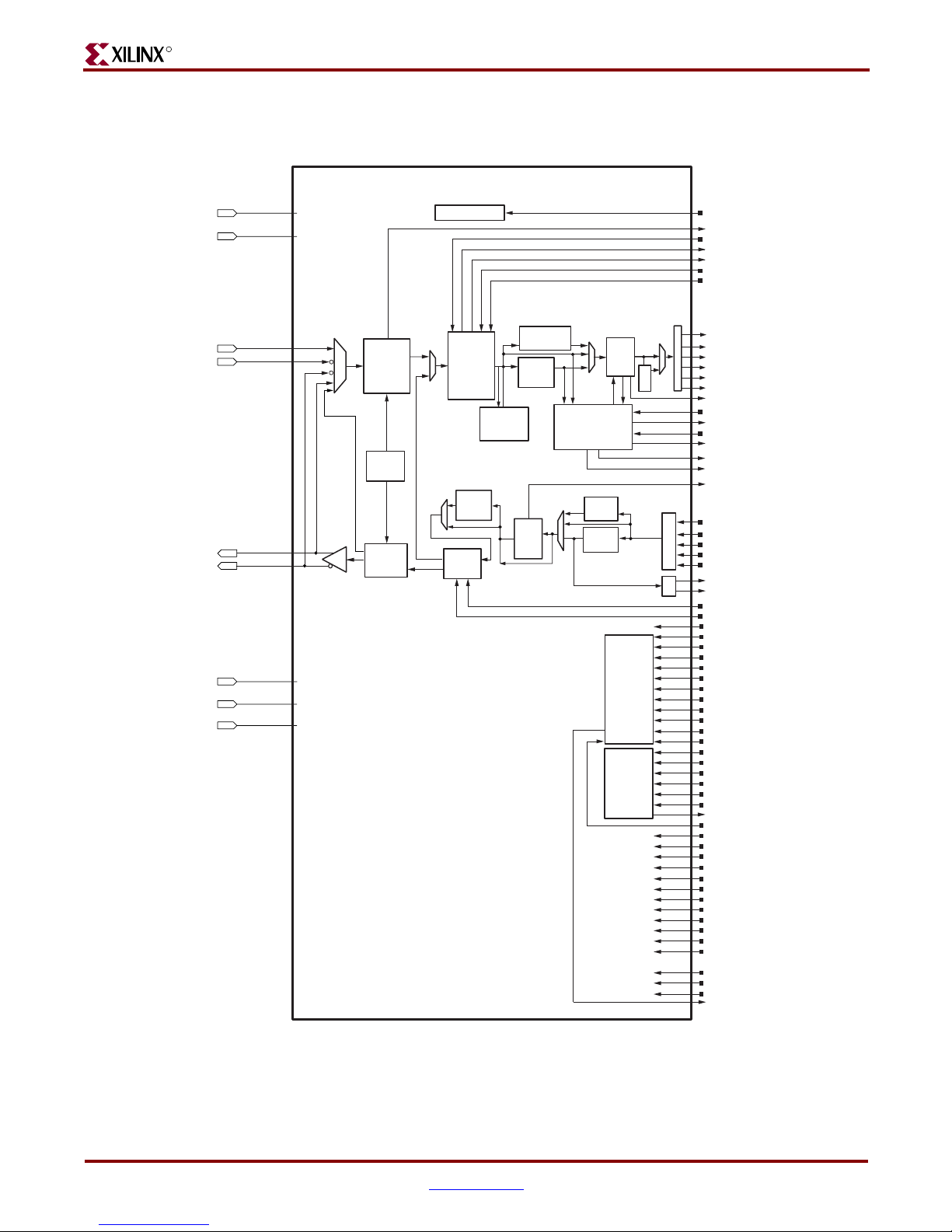
The RocketIO X block diagram is illustrated in Figure 1-1. Depending on the device, a
Virtex-II Pro X FPGA has between 8 and 20 transceiver modules, as shown in Tab le 1 -1.
Definitions:
• Attribute – An attribute is a control parameter to configure the RocketIO X
transceiver. There are both primitive ports (traditional I/O ports for control and
status) and transceiver attributes. Transceiver attributes are also controls to the
transceiver that regulate data widths and encoding rules, but controls that are
configured as a group in “soft” form through the invocation of a primitive.
• GT10 Primitive – A primitive is a pre-designed collection of attribute values that
accomplish a known data rate, encoding type, data width, etc. A single primitive
invocation, for example, OC-192 mode which configures all the dozens of pertinent
attributes to their correct values in a single step.
The transceiver module is designed to operate at any serial bit rate in the range of
2.488 Gb/s to 10.3125 Gb/s per channel, including the specific bit rates used by the
communications standards listed in Tab le 1- 2 , p age 2 7 . Data-rate specific attribute settings
are set appropriately in the GT10 primitives.
Table 1-1: Number of RocketIO X Cores per Device Type
Device RocketIO X Cores
XC2VPX20 8
XC2VPX70 20
Page 26
26 www.xilinx.com RocketIO™ X Transceiver User Guide
1-800-255-7778 UG035 (v1.5) November 22, 2004
Chapter 1: RocketIO X Transceiver Overview
R
Figure 1-1: RocketIO X Transceiver Block Diagram
FPGA FABRIC
MULTI-GIGABIT TRANSCEIVER CORE
Serializer
RXP
TXP
Clock
Manager
Power Down
PACKAGE
PINS
Deserializer
Comma
Detect
Realign
8B/10B
Decoder
TX
FIFO
Channel Bonding
and
Clock Correction
CHBONDI[4:0]
CHBONDO[4:0]
8B/10B
Encoder
RX
Elastic
Buffer
Output
Polarity
RXN
GNDA
TXN
UG035_01_111303
POWERDOWN
RXRECCLK
RXPOLARITY
RXREALIGN
RXCOMMADET
RXRESET
RXCLKCORCNT[2:0]
RXLOSSOFSYNC[1:0]
RXDATA[63:0]
RXNOTINTABLE[7:0]
RXDISPERR[7:0]
RXCHARISK[7:0]
RXCHARISCOMMA[7:0]
RXRUNDISP[7:0]
RXBUFSTATUS[1:0]
ENCHANSYNC
RXUSRCLK
RXUSRCLK2
CHBONDDONE
TXBUFERR
TXDATA[63:0]
TXBYPASS8B10B[7:0]
TXCHARISK[7:0]
TXCHARDISPMODE[7:0]
TXCHARDISPVAL[7:0]
TXKERR[7:0]
TXRUNDISP[7:0]
TXPOLARITY
TXINHIBIT
LOOPBACK[1:0]
TXRESET
REFCLK
REFCLK2
REFCLKSEL
ENPCOMMAALIGN
ENMCOMMAALIGN
TXUSRCLK
TXUSRCLK2
VTRX
AVCCAUXTX
VTTX
AVCCAUXRX
2.5V
TX/RX GND
Termination Supply RX
1.5V
Termination Supply TX
Post Driver Serial Loopback Path
Parallel Loopback Path
BREFCLKP
BREFCLKN
64B/66B
Block Sync
64B/66B
Decoder
Gear
Box
Scrambler
64B/66B
Encoder
PMA
Attribute
Load
PMAREGDATAIN[7:0]
RXCOMMADETUSE
RXDATAWIDTH[1:0]
RXDECC64B66BUSE
PMAINIT
PMAREGADDR[5:0]
PMAREGRW
PMAREGSTROBE
PMARXLOCKSEL[1:0]
PMARXLOCK
RXDEC8B10BUSE
RXDESCRAM64B66BUSE
REFCLKBSEL
RXBLCOKSYNC64B66BUSE
RXSLIDE
TXINTDATAWIDTH[1:0]
TXSCRAM64B66BUSE
TXOUTCLK
RXIGNOREBTF
RXINTDATAWIDTH[1:0]
TXDATAWIDTH[1:0]
TXENC64B66BUSE
TXENC8B10BUSE
TXGEARBOX64B66BUSE
Pre-Driver Loopback Path
64B/66B
Descrambler
Clock /
Reset
Page 27
RocketIO™ X Transceiver User Guide www.xilinx.com 27
UG035 (v1.5) November 22, 2004 1-800-255-7778
Basic Architecture and Capabilities
R
.
Ta bl e 1- 3 lists the transceiver primitives provided. These primitives carry attributes set to
default values for the communications protocols listed in Ta bl e 1 -2 . Data widths of one,
two, and four bytes (lower speeds) or four and eight bytes (higher speeds) are selectable
for the various protocols.
There are three ways to configure the RocketIO X transceiver:
• Static properties can be set through attributes in the HDL code. Use of attributes are
covered in detail in “Primitive Attributes,” page 35.
• Dynamic changes can be made to the attributes via the attribute programming bus.
See Appendix C, “PMA Attribute Programming Bus”for details.
• Dynamic changes can be made through the ports of the primitives.
Table 1-2: Communications Standards Supported by RocketIO X Transceiver
Mode Channels
(1)
(Lanes) I/O Bit Rate (Gb/s)
SONET OC-48 1 2.488
PCI Express 1, 2, 4, 8, 16 2.5
Infiniband 1, 4, 12 2.5
XAUI (10-Gigabit Ethernet) 4 3.125
XAUI (10-Gigabit Fibre Channel) 4 3.1875
SONET OC-192
(2)
1 9.95328
Aurora (Xilinx protocol) 1, 2, 3, 4, ... 2.488 – 10.3125
Custom Mode 1, 2, 3, 4, ... 2.488 – 10.3125
Notes:
1. One channel is considered to be one transceiver.
2. See Solution Record 19020
for implementation recommendations.
Table 1-3: Supported RocketIO X Transceiver Primitives
Primitive Description Primitive Description
GT10_CUSTOM Fully customizable by user GT10_XAUI_4 10GE XAUI, 4-byte data path
GT10_OC48_1 SONET OC-48, 1-byte data path GT10_AURORA_1 Xilinx protocol, 1-byte data path
GT10_OC48_2 SONET OC-48, 2-byte data path GT10_AURORA_2 Xilinx protocol, 2-byte data path
GT10_OC48_4 SONET OC-48, 4-byte data path GT10_AURORA_4 Xilinx protocol, 4-byte data path
GT10_PCI_EXPRESS_1 PCI Express, 1-byte data path GT10_OC192_4 SONET OC-192, 4-byte data path
GT10_PCI_EXPRESS_2 PCI Express, 2-byte data path GT10_OC192_8 SONET OC-192, 8-byte data path
GT10_PCI_EXPRESS_4 PCI Express, 4-byte data path GT10_10GE_4 10Gbit Ethernet, 4-byte data path
GT10_INFINIBAND_1 Infiniband, 1-byte data path GT10_10GE_8 10Gbit Ethernet, 8-byte data path
GT10_INFINIBAND_2 Infiniband, 2-byte data path GT10_10GFC_4 10Gbit Fibre Channel, 4-byte data path
GT10_INFINIBAND_4 Infiniband, 4-byte data path GT10_10GFC_8 10Gbit Fibre Channel, 8-byte data path
GT10_XAUI_1 10GE XAUI, 1-byte data path GT10_AURORAX_4 Xilinx 10G protocol, 4-byte data path
GT10_XAUI_2 10GE XAUI, 2-byte data path GT10_AURORAX_8 Xilinx 10G protocol, 8-byte data path
Page 28
28 www.xilinx.com RocketIO™ X Transceiver User Guide
1-800-255-7778 UG035 (v1.5) November 22, 2004
Chapter 1: RocketIO X Transceiver Overview
R
The RocketIO X transceiver consists of the Physical Media Attachment (PMA) and
Physical Coding Sublayer (PCS). The PMA contains the serializer/deserializer (SERDES),
TX and RX buffers, clock generator, and clock recovery circuitry. The PCS contains the
8B/10B encoder/decoder, 64B/66B encoder/decoder/scrambler/descrambler, and the
elastic buffer supporting channel bonding and clock correction. Refer again to Figure 1-1,
page 26, showing the RocketIO X transceiver top-level block diagram and FPGA interface
signals.
RocketIO X Transceiver Instantiations
For the different clocking schemes, several things must change, including the clock
frequency for USRCLK and USRCLK2 discussed in Chapter 3, “Clocking and Clock
Domains.” The data and control ports for GT10_CUSTOM always use maximum bus
widths. To implement the designs that do not take full advantage of the bus width,
concatenate zeros onto inputs and the wires for outputs for Verilog designs, and set
outputs to open and concatenate zeros on unused input bits for VHDL designs.
HDL Code Examples
The Architecture Wizard can be used to create instantiation templates. This wizard creates
code and instantiation templates that define the attributes for a specific application.
Available Ports
Ta bl e 1- 4 contains the port descriptions of all primitives. The RocketIO X transceiver
primitives contain 72 ports. The differential serial data ports (RXN, RXP, TXN, and TXP)
are connected directly to external pads; the remaining 68 ports are all accessible from the
FPGA logic.
Table 1-4: Primitive Ports
Port I/O Port Size Definition
BREFCLKNIN I 1 Differential BREFCLK negative input from the BREFCLK
pad. See Figure 4-31 and Figure 4-32 for analog
considerations.
BREFCLKPIN I 1 Differential BREFCLK positive input from the BREFCLK
pad. See Figure 4-31 and Figure 4-32 for analog
considerations.
CHBONDDONE O 1 Indicates a receiver has successfully completed channel
bonding when asserted High.
CHBONDI[4:0] I 5 The channel bonding control that is used only by “slaves”
which is driven by a transceiver's CHBONDO port. See
Figure 2-10.
CHBONDO[4:0] O 5 Channel bonding control that passes channel bonding and
clock correction control to other transceivers. See
Figure 2-10.
ENCHANSYNC I 1 Control from the fabric to the transceiver enables the
transceiver to perform channel bonding.
Page 29

RocketIO™ X Transceiver User Guide www.xilinx.com 29
UG035 (v1.5) November 22, 2004 1-800-255-7778
Available Ports
R
ENMCOMMAALIGN I 1 Selects realignment of incoming serial bitstream on minus-
comma. When asserted realigns serial bitstream byte
boundary to where minus-comma is detected.
ENPCOMMAALIGN I 1 Selects realignment of incoming serial bitstream on plus-
comma. When reasserted realigns serial bitstream byte
boundary to where plus-comma is detected.
LOOPBACK[1:0] I 2 Selects the three loopback test modes. These modes are
internal parallel, pre-driver serial, and post-driver serial.
See Table 5-3, page 127 for more information.)
PMAINIT I 1 When asserted High and then deasserted Low, reloads the
PMA coefficients into the PMA from the attribute
PMA_SPEED and then resets the PCS.
PMAREGADDR[5:0] I 6 PMA attribute bus address. This input is asynchronous.
PMAREGDATAIN[7:0] I 8 PMA attribute bus data input. This input is asynchronous.
PMAREGRW I 1 PMA attribute bus read/write control. This input is
asynchronous.
PMAREGSTROBE I 1 PMA attribute bus strobe. Note: This input is asynchronous.
PMARXLOCK O 1 Indicates that the receive PLL has locked in the fine loop.
When RX PLL is set to “Lock to Data,” this signal is always
a logic 1.
PMARXLOCKSEL[1:0] I 2 Selects determination of lock in the receive PLL. See
Tabl e 4-8 , pa ge 10 4.
POWERDOWN I 1 Shuts down both the receiver and transmitter sides of the
transceiver when asserted High. Note: This input is
asynchronous.
REFCLK I 1 The reference clock net that is embedded within the fabric.
REFCLK2 I 1 An alternative to REFCLK. Can be selected by the
REFCLKSEL.
REFCLKBSEL I 1 Selects between BREFCLK and REFCLK/REFCLK2 as
reference clock. Asserted selects BREFCLK. Deasserted
selects REFCLK or REFCLK2, depending on REFCLKSEL.
REFCLKSEL I 1 Selects between REFCLK or REFCLK2 as reference clock.
Deasserted selects REFCLK. Asserted selects REFCLK2.
RXBUFSTATUS[1:0] O 2 Receiver elastic buffer status. Indicates the status of the
receive FIFO pointers, channel bonding skew, and clock
correction events. See “Status and Event Bus,” page 68.
RXBLOCKSYNC64B66BUSE I 1 If asserted, the block sync is used. If deasserted, the block
sync logic is bypassed.
RXCHARISCOMMA[7:0] O 1, 2, 4, 8
(1)
Indicates the reception of K28.0, K28.5, K28.7, and some out
of band commas (depending on the setting of
DEC_VALID_COMMA_ONLY by the 8B/10B decoder.
Table 1-4: Primitive Ports (Continued)
Port I/O Port Size Definition
Page 30

30 www.xilinx.com RocketIO™ X Transceiver User Guide
1-800-255-7778 UG035 (v1.5) November 22, 2004
Chapter 1: RocketIO X Transceiver Overview
R
RXCHARISK[7:0] O 1, 2, 4, 8
(1)
If 8B/10B decoding is enabled, it indicates that the received
data is a “K” character when asserted. Included in Bytemapping. If 8B/10B decoding is bypassed, it remains as the
first bit received (Bit “a”) of the 10-bit encoded data (see
Figure 2-3).
RXCLKCORCNT[2:0] O 3 Status that denotes occurrence of clock correction, channel
bonding, and receive FIFO pointer status. This status is
synchronized on the incoming RXDATA. See “Clock
Correction,” page 63 and “Status and Event Bus,” page 68.
RXCOMMADET O 1 Indicates that the symbol defined by
PCOMMA_10B_VALUE (IF PCOMMA_DETECT is
asserted) and/or MCOMMA_10B_VALUE (if
MCOMMA_DETECT is asserted) has been received.
RXCOMMADETUSE I 1 If asserted High, the comma detect is used. If deasserted, the
comma detect is bypassed.
RXDATA[63:0] O 8, 16, 32, 64
(2)
Up to eight bytes of decoded (8B/10B encoding) or encoded
(8B/10B bypassed) received data at the user fabric.
RXDATAWIDTH[1:0] I 2 (00, 01, 10, 11) Indicates width of FPGA parallel bus. See
“Bus Interface” in Chapter 2.
RXDEC64B66BUSE I 1 If asserted High, the 64/B66B decoder is used. If deasserted,
the 64/66 decoder is bypassed.
RXDEC8B10BUSE I 1 If asserted High, the 8B/10B decoder is used. If deasserted,
the 8b/10b decoder is bypassed.
CLK_COR_8B10B_DE = RXDEC8B10BUSE
RXDESCRAM64B66BUSE I 1 If asserted High, the scrambler is used. If deasserted, the
scrambler is bypassed.
RXDISPERR[7:0] O 1, 2, 4, 8
(1)
If 8B/10B encoding is enabled it indicates whether a
disparity error has occurred on the serial line. Included in
Byte-mapping scheme.
RXIGNOREBTF I 1 If asserted High, the block type field (BTF) is ignored in the
64/66 decoder. Instead of reporting an error, the block is
passed on as is. If deasserted, unrecognized BTFs are
marked as error blocks.
RXINTDATAWIDTH[1:0] I 2 (00, 01, 10, 11) Sets the internal mode of the receive PCS,
either 16, 20, 32, or 40 bit.
RXLOSSOFSYNC[1:0] O 2 Bit 0 is always zero. Bit 1 indicates there is a 64B/66B Block
Lock when deasserted to logic Low.
RXN I 1 Serial differential port (FPGA external)
RXNOTINTABLE[7:0] O 1, 2, 4, 8
(1)
Status of encoded data when the data is not a valid character
when asserted High. Applies to the byte-mapping scheme.
RXP I 1 Serial differential port (FPGA external)
RXPOLARITY I 1 Similar to TXPOLARITY, but for RXN and RXP. When
deasserted, assumes regular polarity. When asserted,
reverses polarity.
Table 1-4: Primitive Ports (Continued)
Port I/O Port Size Definition
Page 31

RocketIO™ X Transceiver User Guide www.xilinx.com 31
UG035 (v1.5) November 22, 2004 1-800-255-7778
Available Ports
R
RXREALIGN O 1 Signal from the PMA denoting that the byte alignment with
the serial data stream changed due to a comma detection.
Asserted High when alignment occurs.
RXRECCLK O 1 Clock recovered from the data stream and divided. Divide
ratio depends on PMA_SPEED setting and/or PMA
attributes. See Appendix C, “PMA Attribute Programming
Bus.”
RXRESET I 1 Synchronous RX system reset that “recenters” the receive
elastic buffer. It also resets 8B/10B decoder, comma detect,
channel bonding, clock correction logic, and other internal
receive registers. It does not reset the receiver PLL.
RXRUNDISP[7:0] O 1, 2, 4, 8
(1)
Signals the running disparity (0 = negative, 1 = positive) in
the received serial data. If 8B/10B encoding is bypassed, it
remains as the second bit received (Bit “b”) of the 10-bit
encoded data.
RXSLIDE I 1 Enables the “slip” of the detection block by 1 bit. To enable
a slide of 1 bit, it increments from a lower bit to a higher bit.
This signal must be asserted and then deasserted
synchronous to RXUSRCKLK2. RXSLIDE must be held Low
for at least two clock cycles before being asserted High
again.
RXUSRC LK I 1 C lock fro m a DCM or a BUFG that is used for readi ng the RX
elastic buffer. It also clocks CHBONDI and CHBONDO in
and out of the transceiver. Typically, the same as
TXUSRCLK.
Note:
RXUSRCLK and RXUSRCLK2 should be 180° out of
phase from each other.
RXUSRCLK2 I 1 Clock output from a DCM that clocks the receiver data and
status between the transceiver and the FPGA fabric.
Typically, the same as TXUSRCLK2.
Note:
RXUSRCLK and RXUSRCLK2 should be 180° out of
phase from each other.
TXBUFERR O 1 Provides status of the transmission FIFO. If asserted High,
an overflow/underflow has occurred. When this bit
becomes set, it can only be reset by asserting TXRESET.
Table 1-4: Primitive Ports (Continued)
Port I/O Port Size Definition
Page 32

32 www.xilinx.com RocketIO™ X Transceiver User Guide
1-800-255-7778 UG035 (v1.5) November 22, 2004
Chapter 1: RocketIO X Transceiver Overview
R
TXBYPASS8B10B[7:0] I 8 If TXENC8B10BUSE = 1 and TXENC64B66BUSE = 0
(8B/10B encoder enabled and 64B/66B encoder disabled),
each bit of TXBYPASS8B10B[7:0] controls the bypass of the
corresponding TXDATA byte; an asserted bit bypasses
encoding for the data in the corresponding byte lane.
If TXENC8B10BUSE = 0 and TXENC64B66BUSE = 1
(8B/10B encoder disabled and 64B/66B encoder enabled),
TXBYPASS8B10B[2:0] bits are used for additional 64B / 66B
encoder block bypass control. TXBYPASS8B10B[7:3] bits are
not relevant in this particular configuration. Bits [2:1] carry
the substitute sync header (SH[1:0]) for the block bypass
operation; bit [0] is asserted for each block that the user
wants to bypass.
TXCHARDISPMODE[7:0] I 1, 2, 4, 8
(1)
If 8B/10B encoding is enabled, this bus determines what
mode of disparity is to be sent. When 8B/10B is bypassed,
this becomes the first bit transmitted (Bit “a”) of the 10-bit
encoded TXDATA bus section (see Table 2 - 6, pag e 49) for
each byte specified by the byte-mapping. The bits have no
meaning if TXENC8B10BUSE is deasserted.
TXCHARDISPVAL[7:0] I 1, 2, 4, 8
(1)
If 8B/10B encoding is enabled, this bus determines what
type of disparity is to be sent. When 8B/10B is bypassed,
this becomes the second bit transmitted (Bit “b”) of the 10bit encoded TXDATA bus section (see Tab le 2-6, page 49) for
each byte specified by the byte-mapping section. The bits
have no meaning if TXENC8B10BUSE is deasserted.
TXCHARISK[7:0] I 1, 2, 4, 8
(1)
If TXENC8B10BUSE = 1 (8B/10B encoder enable), then
TXCHARISK[7:0] signals the K-definition of the TXDATA
byte in the corresponding byte lane. (1 indicates that the
byte is a K character; 0 indicates that the byte is a data
character)
If TXENC64B66BUSE = 1 (64B/66B encoder enable), then
TXCHARISK[3:0] signals the block-formatting definitions
of TXDATA (1 indicates that the byte is a control character;
0 indicates that the byte is a data character).
TXCHARISK[7:4] bits are not relevant in this particular
configuration.
TXDATA[63:0] I 8, 16, 32, 64
(2)
Transmit data from the FPGA user fabric that can be 1, 2, 4,
or 8 bytes wide, depending on the primitive used.
TXDATA[7:0] is always the first byte transmitted. The
position of the first byte depends on selected TX data path
width.
TXDATAWIDTH[1:0] I 2 (00, 01, 10, 11) Indicates width of FPGA parallel bus. See
“Bus Interface” in Chapter 2.
TXENC64B66BUSE I 1 If asserted High, the 64B/66B encoder is used. If deasserted,
the 64/66 encoder is bypassed.
Table 1-4: Primitive Ports (Continued)
Port I/O Port Size Definition
Page 33

RocketIO™ X Transceiver User Guide www.xilinx.com 33
UG035 (v1.5) November 22, 2004 1-800-255-7778
Available Ports
R
TXENC8B10BUSE I 1 If asserted High, the 8B/10B encoder is used. If deasserted,
the 8B/10Bencoder is bypassed.
TXGEARBOX64B66BUSE I 1 If asserted High, the 64B/66B gearbox is used. If deasserted,
the 64/66 gearbox is bypassed.
TXSCRAM64B66USE = TXGEARBOX64B66BUSE
TXINHIBIT I 1 If asserted High, the TX differential pairs are forced to be a
constant 1/0. TXN = 1, TXP = 0
TXINTDATAWIDTH[1:0] I 2 (00, 01, 10, 11) Indicates internal data width (see Tab le 2 -4 ,
page 46).
TXKERR[7:0] O 1, 2, 4, 8
(1)
Indicates even boundary for bypassing in 64B/66B mode.
TXN O 1 Transmit differential port (FPGA external)
TXOUTCLK O 1 Synthesized Clock from RocketIO X transmitter. This clock
can be scaled (e.g., for 64B/66B) relative to BREFCLK,
depending upon the specific operating mode of the
transmitter.
TXP O 1 Transmit differential port (FPGA external)
TXPOLARITY I 1 Specifies whether or not to invert the final transmitter
output. Able to reverse the polarity on the TXN and TXP
lines. Deasserted sets regular polarity. Asserted reverses
polarity.
TXRESET I 1 Synchronous TX system reset that “recenters” the transmit
elastic buffer. It also resets 8B/10B encoder and other
internal transmission registers. It does not reset the
transmission PLL.
TXRUNDISP[7:0] O 1, 2, 4, 8
(1)
Signals the running disparity for its corresponding byte,
after that byte is encoded. Zero equals negative disparity
and positive disparity for a one. This is also overloaded to be
the data output bus of the PMA attribute bus. See Appendix
C, “PMA Attribute Programming Bus”
TXSCRAM64B66BUSE I 1 If asserted High, the 64B/66B scrambler is used. If
deasserted, the 64B/66B scrambler is bypassed.
TXSCRAM64B66USE = TXGEARBOX64B66BUSE
Table 1-4: Primitive Ports (Continued)
Port I/O Port Size Definition
Page 34

34 www.xilinx.com RocketIO™ X Transceiver User Guide
1-800-255-7778 UG035 (v1.5) November 22, 2004
Chapter 1: RocketIO X Transceiver Overview
R
TXUSRCLK I 1 Clock output from a DCM that is clocked with the REFCLK
(or other reference clock). This clock is used for writing the
TX buffer and is frequency-locked to the REFCLK.
Note:
TXUSRCLK and TXUSRCLK2 should be 180° out of phase
from each other.
TXUSRCLK2 I 1 Clock output from a DCM that clocks transmission data and
status and reconfiguration data between the transceiver an
the FPGA fabric. The ratio between the TXUSRCLK and
TXUSRCLK2 depends on the width of the TXDATA.
Note:
TXUSRCLK and TXUSRCLK2 should be 180° out of phase
from each other.
Notes:
1. Port size depends on which primitive is used (1, 2, 4, 8 byte).
2. Port size depends on which primitive is used (8, 16, 32, 64 byte).
Table 1-4: Primitive Ports (Continued)
Port I/O Port Size Definition
Page 35

RocketIO™ X Transceiver User Guide www.xilinx.com 35
UG035 (v1.5) November 22, 2004 1-800-255-7778
Primitive Attributes
R
Primitive Attributes
The primitives also contain attributes set by default to specific values controlling each
specific primitive’s protocol parameters. Included are channel-bonding settings (for
primitives supporting channel bonding), and clock correction sequences. Tabl e 1 -5 shows a
brief description of each attribute. See Appendix F, “Modifiable Attributes”
(Ta bl e F- 1through Tab le F -9 ) for the default values of each primitive.
Table 1-5: RocketIO X Transceiver Attributes
Attribute Type Description
ALIGN_COMMA_WORD
Integer Integer (1, 2, 4) controls the alignment of detected commas within
the transceiver’s 4-byte wide data path. See Tab le 2- 9, p age 5 5.
CHAN_BOND_64B66B_SV
Boolean TRUE/FALSE. This signal is reserved for future use and must be
held to FALSE.
CHAN_BOND_LIMIT
Integer Integer 1-63 that defines maximum number of bytes a slave receiver
can read following a channel bonding sequence and still
successfully align to that sequence.
Note:
This attribute must be set to 16.
CHAN_BOND_MODE
String STRING OFF, MASTER, SLAVE_1_HOP, SLAVE_2_HOPS
OFF: No channel bonding involving this transceiver.
MASTER: This transceiver is master for channel bonding. Its
CHBONDO port directly drives CHBONDI ports on one or more
SLAVE_1_HOP transceivers.
SLAVE_1_HOP: This transceiver is a slave for channel bonding.
SLAVE_1_HOP’s CHBONDI is directly driven by a MASTER
transceiver CHBONDO port. SLAVE_1_HOP’s CHBONDO port
can directly drive CHBONDI ports on one or more SLAVE_2_HOPS
transceivers.
SLAVE_2_HOPS: This transceiver is a slave for channel bonding.
SLAVE_2_HOPS CHBONDI is directly driven by a SLAVE_1_HOP
CHBONDO port.
CHAN_BOND_ONE_SHOT
Boolean FALSE/TRUE that controls repeated execution of channel bonding.
FALSE: Master transceiver initiates channel bonding whenever
possible (whenever channel-bonding sequence is detected in the
input) as long as input ENCHANSYNC is High and RXRESET is
Low.
TRUE: Master transceiver initiates channel bonding only the first
time it is possible (channel bonding sequence is detected in input)
following negated RXRESET and asserted ENCHANSYNC. After
channel-bonding alignment is done, it does not occur again until
RXRESET is asserted and negated, or until ENCHANSYNC is
negated and reasserted.
Slave transceivers should always have CHAN_BOND_ONE_SHOT
set to FALSE.
Page 36

36 www.xilinx.com RocketIO™ X Transceiver User Guide
1-800-255-7778 UG035 (v1.5) November 22, 2004
Chapter 1: RocketIO X Transceiver Overview
R
CHAN_BOND_SEQ_1_*[10:0]
11-bit
vector
These define the channel bonding sequence. The usage of these
vectors also depends on CHAN_BOND_SEQ_LEN and
CHAN_BOND_SEQ_2_USE. See “Transmitting Vitesse Channel
Bonding Sequence,” page 52, for format.
CHAN_BOND_SEQ_1_MASK[3:0]
4-bit
vector
Each bit of the mask determines if that particular sequence is
detected regardless of its value. If bit 0 is High, then
CHAN_BOND_SEQ_1_1 is matched regardless of its value.
CHAN_BOND_SEQ_2_*[10:0]
11-bit
vector
These define the channel bonding sequence: The usage of these
vectors also depends on CHAN_BOND_SEQ_LEN and
CHAN_BOND_SEQ_2_USE. See “Receiving Vitesse Channel
Bonding Sequence,” page 52, for format.
CHAN_BOND_SEQ_2_MASK[3:0]
4-bit
vector
Each bit of the mask determines if that particular sequence is
detected regardless of its value. If bit 0 is High, then
CHAN_BOND_SEQ_2_1 is matched regardless of its value.
CHAN_BOND_SEQ_2_USE
Boolean FALSE/TRUE that controls use of second channel bonding
sequence.
FALSE: Channel bonding uses only one channel bonding sequence
defined by CHAN_BOND_SEQ_1_1 ... 4, or one 8-byte sequence
defined by CHAN_BOND_SEQ_1_X and CHAN_BOND_SEQ_2_X
in combination.
TRUE: Channel bonding uses two channel bonding sequences
defined by CHAN_BOND_SEQ_1_1 ... 4 and
CHAN_BOND_SEQ_2_1 ... 4, as further constrained by
CHAN_BOND_SEQ_LEN.
CHAN_BOND_SEQ_LEN
Integer Integer (1, 2, 3, 4, 8) defines length in bytes of channel bonding
sequence. This defines the length of the sequence the transceiver
matches to detect opportunities for channel bonding.
CLK_COR_8B10B_DE
Boolean This signal selects if clock correction occurs relative to the encoded or
decoded version of the 8B/10B stream. If set to TRUE, the decoded
version is used. If set to FALSE, the encoded version is used. Must be
set in conjunction with RXDEC8B10USE.
CLK_COR_8B10B_DE = RXDEC8B10BUSE
CLK_COR_MAX_LAT
Integer (0-63) Integer defines the upper bound of the receive FIFO.
Note:
This attribute is recommended to be set to 48.
CLK_COR_MIN_LAT
Integer (0-63) Integer defines the lower bound of the receive FIFO.
Note:
This attribute is recommended to be set to 32.
CLK_COR_SEQ_1_*[10:0]
11-bit
vector
These define the sequence for clock correction. The attribute used
depends on the CLK_COR_SEQ_LEN and CLK_COR_SEQ_2_USE.
CLK_COR_SEQ_1_MASK[3:0]
4-bit
vector
Each bit of the mask determines if that particular sequence is
detected regardless of its value. If bit 0 is High, then
CLK_COR_SEQ_1_1 is matched regardless of its value.
CLK_COR_SEQ_2_*[10:0]
11-bit
vector
These define the sequence for clock correction. The attribute used
depends on the CLK_COR_SEQ_LEN and CLK_COR_SEQ_2_USE.
Table 1-5: RocketIO X Transceiver Attributes (Continued)
Attribute Type Description
Page 37

RocketIO™ X Transceiver User Guide www.xilinx.com 37
UG035 (v1.5) November 22, 2004 1-800-255-7778
Primitive Attributes
R
CLK_COR_SEQ_2_MASK[3:0]
4-bit
vector
Each bit of the mask determines if that particular sequence is
detected regardless of its value. If bit 0 is High, then
CLK_COR_SEQ_2_1 is matched regardless of its value.
CLK_COR_SEQ_2_USE
Boolean FALSE/TRUE Control use of second clock correction sequence.
FALSE: Clock correction uses only one clock correction sequence
defined by CLK_COR_SEQ_1_1 ... 4, or one 8-byte sequence defined
by CLK_COR_SEQ_1_X and CLK_COR_SEQ_2_X in combination.
TRUE: Clock correction uses two clock correction sequences
defined by CLK_COR_SEQ_1_1 ... 4 and CLK_COR_SEQ_2_1 ... 4,
as further constrained by CLK_COR_SEQ_LEN.
CLK_COR_SEQ_DROP
Boolean TRUE/FALSE. When asserted TRUE, the clock correction mode is
via idle removal. When FALSE, the clock correction mode is via idle
removal or insertion.
Note:
This attribute must be set to FALSE.
CLK_COR_SEQ_LEN
Integer Integer (1, 2, 3, 4, 8) that defines the length of the sequence the
transceiver matches to detect opportunities for clock correction. It
also defines the size of the correction, since the transceiver executes
clock correction by repeating or skipping entire clock correction
sequences.
CLK_CORRECT_USE
Boolean TRUE/FALSE controls the use of clock correction logic.
FALSE: Permanently disable execution of clock correction (rate
matching). Clock RXUSRCLK must be frequency-locked with
RXRECCLK in this case.
TRUE: Enable clock correction (normal mode).
COMMA_10B_MASK[9:0]
10-bit
vector
These define the mask that is ANDed with the incoming
serial-bit stream before comparison against
PCOMMA_10B_VALUE and MCOMMA_10B_VALUE.
DEC_MCOMMA_DETECT
Boolean TRUE/FALSE controls the raising of per-byte flag
RXCHARISCOMMA on minus-comma.
DEC_PCOMMA_DETECT
Boolean TRUE/FALSE controls the raising of per-byte flag
RXCHARISCOMMA on plus-comma.
DEC_VALID_COMMA_ONLY
Boolean TRUE/FALSE controls the raising of RXCHARISCOMMA on an
invalid comma.
FALSE: Raise RXCHARISCOMMA on:
xxx1111100 (if DEC_PCOMMA_DETECT is TRUE)
and/or on:
xxx0000011 (if DEC_MCOMMA_DETECT is TRUE)
or on 8B/10B translation commas
regardless of the settings of the xxx bits.
TRUE: Raise RXCHARISCOMMA only on valid characters that are
in the 8B/10B translation.
Table 1-5: RocketIO X Transceiver Attributes (Continued)
Attribute Type Description
Page 38

38 www.xilinx.com RocketIO™ X Transceiver User Guide
1-800-255-7778 UG035 (v1.5) November 22, 2004
Chapter 1: RocketIO X Transceiver Overview
R
MCOMMA_10B_VALUE[9:0]
10-bit
vector
These define minus-comma for the purpose of raising
RXCOMMADET and realigning the serial bit stream byte boundary.
This definition does not affect 8B/10B encoding or decoding. Also
see COMMA_10B_MASK.
MCOMMA_DETECT
Boolean TRUE/FALSE indicates whether to raise or not raise the
RXCOMMADET when minus-comma is detected.
PCOMMA_10B_VALUE[9:0]
10-bit
vector
These define plus-comma for the purpose of raising
RXCOMMADET and realigning the serial bit stream byte boundary.
This definition does not affect 8B/10B encoding or decoding. Also
see COMMA_10B_MASK.
PCOMMA_DETECT
Boolean TRUE/FALSE indicates whether to raise or not raise the
RXCOMMADET when plus-comma is detected.
PMA_PWR _CNTRL
Integer This masks the startup sequence of the PMA and must always be set
to all ones.
PMA_SPEED
String (13_40) Selects the mode of the PMA. Refer to PMA section for the
proper mode selection.
RX_BUFFER_USE
Boolean TRUE/FALSE. Recommended to always be set to TRUE. Enables the
use of the receive side buffer. When set to TRUE, the buffer is enabled.
RX_LOS_INVALID_INCR[7:0]
Integer Power of two in a range of 1 to 128 that denotes the number of valid
characters required to "cancel out" appearance of one invalid
character for loss of sync determination.
RX_LOS_THRESHOLD
Integer Power of two in a range of 4 to 512. When divided by
RX_LOS_INVALID_INCR, denotes the number of invalid
characters required to cause FSM transition to “sync lost” state.
RX_LOSS_OF_SYNC_FSM
Boolean Undefined.
SH_CNT_MAX[7:0]
8-bit
vector
8-bit binary; controls when the 64B/66B synchronization state
machine enters synchronization. (max sync header count)
SH_INVALID_CNT_MAX[7:0]
8-bit
vector
8-bit binary; controls when the 64B/66B synchronization state
machine leaves synchronization. (max invalid sync header count)
TX_BUFFER_USE
Boolean When set to TRUE, this enables the use of the transmit buffer.
Table 1-5: RocketIO X Transceiver Attributes (Continued)
Attribute Type Description
Page 39

RocketIO™ X Transceiver User Guide www.xilinx.com 39
UG035 (v1.5) November 22, 2004 1-800-255-7778
Modifiable Attributes
R
Modifiable Attributes
As shown in Appendix F, “Modifiable Attributes” (Ta bl e F- 1 through Ta b le F -9 ) only
certain attributes are modifiable for any primitive. These attributes help to define the
protocol used by the primitive. Only the GT10_CUSTOM primitive allows the user to
modify all of the attributes to a protocol not supported by another transceiver primitive.
This allows for complete flexibility. The other primitives allow modification of the analog
attributes of the serial data lines and several channel-bonding values.
Byte Mapping
Most of the 8-bit wide status and control buses correlate to a specific byte of the TXDATA
or RXDATA. This scheme is shown in Tab le 1 -6. This creates a way to tie all the signals
together regardless of the data path width needed for the GT10_CUSTOM. All other
primitives with specific data width paths and all byte-mapped ports are affected by this
situation. For example, a 1-byte wide data path has only 1-bit control and status bits
(TXCHARISK[0]) correlating to the data bits TXDATA[7:0].
Table 1-6: Control/Status Bus Association to Data Bus Byte Paths
Control/Status Bit Data Bits
[0] [7:0]
[1] [15:8]
[2] [23:16]
[3] [31:24]
[4] [39:32]
[5] [47:40]
[6] [55:48]
[7] [64:56]
Page 40

40 www.xilinx.com RocketIO™ X Transceiver User Guide
1-800-255-7778 UG035 (v1.5) November 22, 2004
Chapter 1: RocketIO X Transceiver Overview
R
Page 41

RocketIO™ X Transceiver User Guide www.xilinx.com 41
UG035 (v1.5) November 22, 2004 1-800-255-7778
R
Chapter 2
Digital Design Considerations
The Physical Coding Sublayer (PCS) portion of the RocketIO X transceiver has been
significantly updated relative to the RocketIO. The RocketIO X PCS supports 8B/10B and
64B/66B encode/decode, SONET compatibility, and generic data modes. The RocketIO X
transceiver operates in four basic internal modes: 16 bit, 20 bit, 32 bit, and 40 bit. When
accompanied by the predefined modes of the Physical Media Attachment (PMA), the user
has a large combination of protocols and data rates from which to choose. With the custom
RocketIO X transceiver, the user has an almost infinite amount of possibilities from which
to choose in constructing the most advanced and easily configurable communication paths
in the history of communication ICs.
The RocketIO X PCS also represents a shift in the configurability of transceivers. This
allows the user to change not only speeds of the PMA in real time, but also protocols
within the PCS. Internal data width, external data width, and data routing can all be
configured on a clock-by-clock basis. With this advancement, users can initialize a
communication channel at a low speed (for example, 2.5 Gb/s using 8B/10B (20 bit
internal) and then auto-negotiate after the channel is stable to a 10.3125 Gb/s speed using
64B/66B (32 bit internal).
Note:
The information in this chapter is provided to RocketIO X users as a reference for
understanding the individual attribute and control port settings within a primitive. Users have the
choice of using the supported primitives in Table 1-3, page 27, and ignoring this chapter, or using this
chapter to better understand PCS configuration and/or to modify attribute and port values to create a
user transceiver configuration.
Page 42

42 www.xilinx.com RocketIO™ X Transceiver User Guide
1-800-255-7778 UG035 (v1.5) November 22, 2004
Chapter 2: Digital Design Considerations
R
Top-Level Architecture
Transmit Architecture
The transmit architecture for the PCS is shown in Figure 2-1. For information about
bypassing particular blocks, consult the block function section for that particular block.
Receive Architecture
The receive architecture for the PCS is shown in Figure 2-2. For information about
bypassing particular blocks, consult the block function section for that particular block.
Figure 2-1: Transmit Architecture
6x40 bit
TXFIFO
8B/10B
Encode
Gearbox
10G Encode
TXUSRCLK
TXUSRCLK2
TXENC8B10BUSE
TXENC6466USE
TXSCRAM64B66BUSE
TXGEARBOX64B66BUSE
TXPOLARITY
PMA
Scrambler
PMA
Convert
TX_BUFFER_USE
Reset
Control
PMA
Attribute
Load
Fabric Convert
PMAINIT
UG035_CH3_01_092903
TXDATA
TXRESET
TXP
TXN
Figure 2-2: Receive Architecture
RXCLK0
PMA/PCS Boundary
RX Elastic
Buffer
16x52
Channel Bonding & Clock
Correction
Fabric
8B/10B
Decode
Comma Detect
Align
10G
Block
Sync
10G
Decode
10G
Descr
RXRECCLK
RXUSRCLK
RXUSRCLK2
Sync State Machine
RXBLOCKSYNCUSE,
RXVALUEDETUSE
RXDEC8B10BUSE,
RXDESCRAM64B66BUSE
RX_BUFFER_USE
RXDEC6466USE
SLIP
Reset Control
HOLDOFF
UG035_CH3_02_092903
ENPCOMMAALIGN
ENMCOMMAALIGN
RXPOLARITY
LOCK
CHBOND
RX Data Word Alignment Mux
RXDATA
RXRESET
Page 43

RocketIO™ X Transceiver User Guide www.xilinx.com 43
UG035 (v1.5) November 22, 2004 1-800-255-7778
Block Level Functions
R
Operation Modes
Internally, there are four modes of operation within the PCS: 16 bit, 20 bit, 32 bit, and 40 bit.
The PCS fundamentally operates in either 2-byte mode, or 4-byte mode, with 2-byte mode
corresponding to 16- and 20-bit mode, and with 4-byte mode corresponding to 32- and 40bit mode. When in 2-byte mode, the external interface can either be one, two, or four bytes
wide. When in 4-byte mode, the external interface can either be 4 or 8 bytes wide. It is not
possible to have an internal 2-byte width and an 8-byte external interface. It is also not
possible to have an internal 4-byte interface, along with a 1-byte external interface. See
Ta bl e 2- 1.
A general guide to use is that 2-byte mode should be used in the PCS when the serial speed
is below 5 Gb/s, and the 4-byte mode should be used when the serial speed is greater than
5 Gb/s. In 2-byte mode, the PCS processes 4-byte data every other byte. This is transparent
to the user, but skews between transceivers result in larger bit skews at the transmit
interface as compared to Virtex-II Pro transceivers. Any one of the three encoding schemes
(8B/10B and 64B/66B encode/decode, SONET, and generic data modes) can be used in
either 2- or 4-byte mode, with each block having a bypass ability.
For more information on setting the PCS mode, refer to the block functional definition of
the bus interface in this guide.
Block Level Functions
Classification of Signals and Overloading
This section describes the pertinent signals at the interface of the PCS and how to prioritize
them. For more information about a particular signal, refer to the I/O specification, or the
particular block function of interest.
Static Signals (Control Inputs)
The following static signals are inputs that control the internal and external mode of
operation in the PCS. Typically, these signals would be the first consideration after the
mode of operation has been selected:
• RXDATAWIDTH[1:0]
• RXINTDATAWIDTH[1:0]
• TXDATAWIDTH[1:0]
• TXINTDATAWIDTH[1:0]
Table 2-1: PCS Interface Choice
Speed 2 Byte (internal mode) 4 Byte (internal mode)
2.488 Gb/s recommended do not use
5 - 10.3125 Gb/s do not use recommended
Page 44

44 www.xilinx.com RocketIO™ X Transceiver User Guide
1-800-255-7778 UG035 (v1.5) November 22, 2004
Chapter 2: Digital Design Considerations
R
The following static signals are inputs that control the PCS interblock routing and bypass
for particular blocks, which adjust the architecture of the PCS for the user’s particular
application:
• RXBLOCKSYNC64B66BUSE
• RXDEC64B66BUSE
• RXDEC8B10BUSE
• RXDESCRAM64B66BUSE
• RXCOMMADETUSE
• TXENC64B66BUSE
• TXENC8B10BUSE
• TXGEARBOX64B66BUSE
• TXSCRAM64B66BUSE
The following static signals are inputs that control various functions, but are usually set
once at the beginning of a state machine, or after an auto-negotiation sequence. They are
typically not altered on a clock-by-clock basis:
• ALIGN_COMMA_WORD
• ENMCOMMAALIGN
• ENPCOMMAALIGN
• RXPOLARITY
• TXPOLARITY
• PMAINIT
• RXIGNOREBTF
• PMARXLOCKSEL[1:0]
The following static signals are inputs that cause either major functional resets or are used
in troubleshooting. These signals are mostly used at initialization, not during the
functional operation of the circuit:
• LOOPBACK[1:0] (Note: This signal can also be a dynamic signal.)
• POWERDOWN
• RXRESET
• TXRESET
• TXINHIBIT
Dynamic Signals
The following dynamic signals indicate data received on the receive bus, along with status
signals that indicate specific information about RXDATA. The set values of these signals
define the application setup by the user and are the most important after the static signals
are allocated:
• MCOMMA_10B_VALUE
• PCOMMA_10B_VALUE
• COMMA_10B_MASK
• RXCHARISCOMMA[7:0]
• RXCHARISK[7:0]
Page 45

RocketIO™ X Transceiver User Guide www.xilinx.com 45
UG035 (v1.5) November 22, 2004 1-800-255-7778
Block Level Functions
R
• RXDISPERR[7:0]
• RXNOTINTABLE[7:0]
• RXDATA[63:0]
The following dynamic signals indicate data to be transmitted on the transmit bus, along
with status signals that indicate specific information about how TXDATA is to be handled
while passing through the PCS. The set values of these signals define the application setup
by the user and are the most important after the static signals are allocated:
• TXBYPASS8B10B[7:0]
• TXCHARDISPMODE[7:0]
• TXCHARDISPVAL[7:0]
• TXCHARISK[7:0]
• TXDATA[63:0]
The following dynamic signals indicate various status information about the current state
or prior state of the PCS:
• CHBONDDONE, RXBUFSTATUS[1:0], RXCLKCORCNT[2:0]
• CHBONDO[4:0]
• PMARXLOCK
• RXLOSSOFSYNC[1:0]
• RXREALIGN
• RXCOMMADET
• TXBUFERR
• TXKERR[7:0]
• TXRUNDISP[7:0]
• RXRUNDISP[7:0]
The following dynamic signals control internal states of the PCS:
• RXSLIDE
• CHBONDI[4:0]
The following dynamic signals affect the control registers of the PMA:
• PMAREGADDR[5:0]
• PMAREGDATAIN[7:0]
• PMAREGRW
• PMAREGSTROBE
Page 46

46 www.xilinx.com RocketIO™ X Transceiver User Guide
1-800-255-7778 UG035 (v1.5) November 22, 2004
Chapter 2: Digital Design Considerations
R
Bus Interface
Selecting the External Configuration (Fabric Interface)
By using the signals TXDATAWIDTH[1:0] and RXDATAWIDTH[1:0], the fabric interface
can be determined.
Selecting the Internal Configuration
Clock Ratio
USRCLK2 clocks the data buffers. The ability to send parallel data to the transceiver at four
different widths requires the user to change the frequency of USRCLK2. This creates a
frequency ratio between USRCLK and USRCLK2. The falling edges of the clocks must
align. See Ta bl e 2- 4.
Table 2-2: Selecting the External Configuration
RXDATAWIDTH/TXDATAWIDTH Data Width
Internal Bus
Requirements
2’b00 8/10 bit (1 byte) 16, 20 bit mode
2’b01 16/20 bit (2 byte) 16, 20 bit mode
2’b10 32/40 bit (4 byte) 16, 20, 32, 40 bit mode
2’b11 64/80 bit (8 byte) 32, 40 bit mode
Table 2-3: Selecting the Internal Configuration
RXINTDATAWIDTH/TXINTDATAWIDTH Internal Data Width
2’b00 16 bit
2’b01 20 bit
2’b10 32 bit
2’b11 40 bit
Table 2-4: Data Width Clock Ratios
Fabric Data Width
Frequency Ratio of USRCLK\USRCLK2
2-Byte Internal Data Width 4-Byte Internal Data Width
1 byte 1:2
(1)
N/A
2 byte 1:1 N/A
4 byte 2:1
(1)
1:1
8 byte N/A 2:1
(1)
Notes:
1. Each edge of slower clock must align with falling edge of faster clock.
Page 47

RocketIO™ X Transceiver User Guide www.xilinx.com 47
UG035 (v1.5) November 22, 2004 1-800-255-7778
Block Level Functions
R
8B/10B
Note: In the RocketIO transceiver, the most significant byte was sent first; in the RocketIO X
transceiver the least significant byte is sent first.
The following sections categorize the ports and attributes of the transceiver according to
specific functionality including 8B/10B encoding/decoding, 64B/66B
encoding/decoding, SERDES alignment, clock correction (clock recovery), channel
bonding, fabric interface, and other signals.
The 8B/10B encoding translates an 8-bit parallel data byte to be transmitted into a 10-bit
serial data stream. This conversion and data alignment are shown in Figure 2-3. The serial
port transmits the least significant bit of the 10-bit data, “a” first and proceeds to “j”. This
allows data to be read and matched to the form shown in Appendix B, “8B/10B Valid
Characters.”.
The serial data bit sequence is dependent on the width of the parallel data. The least
significant byte is always sent first regardless of the whether 1-byte, 2-byte, 4-byte or 8byte paths are used. The most significant byte is always last. Figure 2-4 shows a case when
the serial data corresponds to each byte of the parallel data. TXDATA[7:0] is serialized and
sent out first followed by TXDATA[15:8], TXDATA[23:16], and finally TXDATA[31:24]. The
2-byte path transmits TXDATA[7:0] and then TXDATA[15:8].
Figure 2-3: 8B/10B Parallel-to-Serial Conversion
Figure 2-4: 4-Byte Serial Structure
UG024_10_021102
01234576
ABCDEFHG
Parallel
7896543201
ghjfiedcab
Serial
8B/10B
First transmitted Last transmitted
ug035_ch3_22_111303
TXDATA 31:24 TXDATA 23:16 TXDATA 15:8 TXDATA 7:0
H3 − A
3
H2 − A
2
H1 − A
1
H0 − A
0
a3 − j
3
a2 − j
2
a1 − j
1
a0 − j
0
8B/10B
LSB
3
LSB
2
LSB
1
LSB
0
1
st
Sent
Encoded
2nd Sent
Encoded
3rd Sent
Encoded
4th Sent
Encoded
Page 48

48 www.xilinx.com RocketIO™ X Transceiver User Guide
1-800-255-7778 UG035 (v1.5) November 22, 2004
Chapter 2: Digital Design Considerations
R
Encoder
A bypassable 8B/10B encoder is included in the transmitter. The encoder uses the same
256 data characters and 12 control characters (shown in Appendix B, “8B/10B Valid
Characters”) that are used for Gigabit Ethernet, XAUI, Fibre Channel, and InfiniBand.
The encoder accepts 8 bits of data along with a K-character signal for a total of 9 bits per
character applied. If the K-character signal is High, the data is encoded into one of the 12
possible K-characters available in the 8B/10B code. If the K-character input is Low, the
8 bits are encoded as standard data.
There are two ports that enable the 8B/10B encoding in the transceiver. The
TXBYPASS8B10B is a byte-mapped port that is 1, 2, 4 or 8 bits depending on the data width
of the transceiver primitive being used. These bits correlate to each byte of the data path.
To enable the 8B/10B encoding of the transmitter, these bits should be set to a logic 0. In
this mode, the transmit data that is input to the TXDATA port is non-encoded data of either
8, 16, 32, or 64 bits wide. However, if other encoding schemes are preferred, the encoder
capabilities are bypassed by setting all bits to a logic 1. The extra bits are fed through the
TXCHARDISPMODE and TXCHARDISPVAL buses.
TXCHARDISPVAL and TXCHARDISPMODE
TXCHARDISPVAL and TXCHARDISPMODE are dual-purpose ports for the transmitter
depending whether 8B/10B encoding is done. Ta bl e 2 -6 shows this dual functionality.
When encoding is enabled, these ports function as byte-mapped control ports controlling
the running disparity of the transmitted serial data (Ta bl e 2 -5 ).
In the encoding configuration, the disparity of the serial transmission can be controlled
with the TXCHARDISPVAL and TXCHARDISPMODE ports. When TXCHARDISPMODE
is set to a logic 1, the running disparity is set before encoding the specific byte.
TXCHARDISPVAL determines if the disparity is negative (set to a logic 0) or positive (set
to a logic 1).
When TXCHARDSIPMODE is set to a logic 0, the running disparity is maintained if
TXCHARDISPVAL is also set to a logic 0. However, the disparity is inverted before
encoding the byte when the TXCHARDISPVAL is set to a logic 1.
Most applications use the mode where both TXCHARDISPMODE and TXCHARDISPVAL
are set to logic 0. Some applications can use other settings if special running disparity
configurations are required, such as in the “Vitesse Disparity Example,” page 52.
In the bypassed configuration, TXCHARDISPMODE[0] becomes bit 9 of the 10 bits of
encoded data (TXCHARDISPMODE[1:7] are bits 19, 29, 39, 49, 59, 69, and 79 in the 20-bit
and 40-bit and 80-bit wide buses). TXCHARDISPVAL becomes bits 8, 18, 28, 38, 48, 58, 68,
and 78 of the transmit data bus while the TXDATA bus completes the bus. See Tab le 2 -6.
Table 2-5: Running Disparity Control
{txchardispmode,
txchardispval}
Function
00 Maintain running disparity normally
01 Invert normally generated running disparity before
encoding this byte
10 Set negative running disparity before encoding this byte
11 Set positive running disparity before encoding this byte
Page 49

RocketIO™ X Transceiver User Guide www.xilinx.com 49
UG035 (v1.5) November 22, 2004 1-800-255-7778
Block Level Functions
R
During transmit, while 8B/10B encoding is enabled, the disparity of the serial
transmission can be controlled with the TXCHARDISPVAL and TXCHARDISPMODE
ports. When 8B/10B encoding is bypassed, these bits become Bits “b” and “a,”
respectively, of the 10-bit encoded data that the transceiver must transmit to the receiving
terminal. Figure 2-5 illustrates the TX data map during 8B/10B bypass.
TXCHARISK
TXCHARISK is a byte-mapped control port that is only used when the 8B/10B encoder is
implemented. This port indicates whether the byte of TXDATA is to be encoded as a
control (K) character when asserted and data character when de-asserted. When 8B/10B
encoding is bypassed this port is undefined.
TXRUNDISP
TXRUNDISP is a status port that is byte-mapped to the TXDATA. This port indicates the
running disparity after this byte of TXDATA is encoded. When asserted, the disparity is
positive. When de-asserted, the disparity is negative.
Table 2-6: 8B/10B Bypassed Signal Significance
Signal Function
TXBYPASS8B10B
(1)
0 8B/10B encoding is enabled (not bypassed)
1 8B/10B encoding bypassed (disabled)
TXCHARDISPMODE,
TXCHARDISPVAL
Function, 8B/10B Enabled Function, 8B/10B Bypassed
00 Maintain running disparity normally Part of 10-bit encoded byte
(see Figure 2-5):
TXCHARDISPMODE[0],
(or: [1] / [2] / [3] /[4]/[5]/[6]/[7])
TXCHARDISPVAL[0],
(or: [1] / [2] / [3] /[4]/[5]/[6]/[7])
TXDATA[7:0]
(or: [15:8] / [23:16] / [31:24]/
[39:32]/[47:40]/[55:48]/[63:56})
01 Invert the normally generated running
disparity before encoding this byte.
10 Set negative running disparity before
encoding this byte.
11 Set positive running disparity before
encoding this byte.
TXCHARISK Received byte is a K-character Unused
Notes:
1. If 8B/10B is bypassed, this port can be defined if 64B/66B encoding is used.
Figure 2-5: 10-Bit TX Data Map with 8B/10B Bypassed
UG024_10a_080404
7896543201
Last transmitted First transmitted
TXCHARDISPMODE[0]
TXCHARDISPVAL[0]
TXDATA[7] . . . . . . TXDATA[0]
cbadeifgjh
Page 50

50 www.xilinx.com RocketIO™ X Transceiver User Guide
1-800-255-7778 UG035 (v1.5) November 22, 2004
Chapter 2: Digital Design Considerations
R
Decoder
An optional 8B/10B decoder is included in the receiver. A programmable option allows the
decoder to be bypassed. When the 8B/10B decoder is bypassed, the 10-bit character order
is shown in Figure 2-6 for a graphical representation of the received 10-bit character.
The decoder uses the same table (see Appendix B, “8B/10B Valid Characters”) that is used
for Gigabit Ethernet, Fibre Channel, and InfiniBand. In addition to decoding all data and
K-characters, the decoder has several extra features. The decoder separately detects both
“disparity errors” and “out-of-band” errors. A disparity error occurs when a 10-bit character
is received that exists within the 8B/10B table, but has an incorrect disparity. An out-of-band
error occurs when a 10-bit character is received that does not exist within the 8B/10B table.
It is possible to obtain an out-of-band error without having a disparity error, or more
commonly, a disparity error is possible without an out-of-band error. The proper disparity
is always computed for both legal and illegal characters. The current running disparity is
available at the RXRUNDISP signal.
The 8B/10B decoder performs a unique operation if out-of-band data is detected. If out-ofband data is detected, the decoder signals the error and passes the illegal 10-bits through
and places them on the outputs. This can be used for debugging purposes if desired.
The decoder also signals reception of one of the 12 valid K-characters. In addition, a
programmable comma detect is included. The comma detect signal registers a comma on
the receipt of any comma+, comma–, or both. Since the comma is defined as a 7-bit
character, this includes several out-of-band characters. Another option allows the decoder
to detect only the three defined commas (K28.1, K28.5, and K28.7) as comma+, comma–, or
both. In total, there are six possible options, three for valid commas and three for “any
comma.”
Note that all bytes (1, 2, 4 or 8) at the RX FPGA interface each have their own individual
8B/10B indicators (K-character, disparity error, out-of-band error, current running
disparity, and comma detect).
During receive, while 8B/10B decoding is enabled, the running disparity of the serial
transmission can be read by the transceiver from the RXRUNDISP port, while the
RXCHARISK port indicates presence of a K-character. When 8B/10B decoding is
bypassed, these bits remain as Bits “b” and “a,” respectively, of the 10-bit encoded data that
the transceiver passes on to the user logic. Tab le 2 -7 illustrates the RX data map during
8B/10B bypass.
Figure 2-6: 10-Bit RX Data Map with 8B/10B Bypassed
UG024_10b_080404
7896543201
Last received First received
RXCHARISK[0]
RXRUNDISP[0]
RXDATA[7] . . . . . . RXDATA[0]
cbadeifgjh
Page 51

RocketIO™ X Transceiver User Guide www.xilinx.com 51
UG035 (v1.5) November 22, 2004 1-800-255-7778
Block Level Functions
R
RXCHARISK and RXRUNDISP
RXCHARISK and RXRUNDISP are dual-purpose ports for the receiver depending
whether 8B/10B decoding is enabled. Figure 2-8 shows this dual functionality. When
decoding is enabled, these ports function as byte-mapped status ports of the received
data.
In the encoding configuration, when RXCHARISK is asserted that byte of the received data
is a control (K) character. Otherwise, the received byte of data is a data character. (See
Appendix B, “8B/10B Valid Characters”). The RXRUNDISP port indicates the disparity of
the received byte is either negative or positive. RXRUNDISP is asserted to indicate positive
disparity. This is used in cases like the “Vitesse Disparity Example,” page 52.
In the bypassed configuration, RXCHARISK and RXRUNDISP are additional data bits for
the 10-,
20-, 40-, or 80-bit buses. This is similar to the transmit side. RXCHARISK[0:7] relates to bits
9, 19, 29, 39, 49, 59, 69, and 79 while RXRUNDISP pertains to bits 8, 18, 28, 38, 48, 58, 68, and
78 of the data bus. See Figure 2-8.
RXDISPERR
RXDISPERR is a status port for the receiver that is byte-mapped to the RXDATA. When a
bit is asserted, a disparity error occurred on the received data. This usually indicated that
the data is corrupt by bit errors, transmission of an invalid control character, or for cases
when normal disparity is not required such as in the “Vitesse Disparity Example,” page 52.
RXNOTINTABLE
RXNOTINTABLE is asserted whenever the received data is not in the 8B/10B tables. The
data received on bytes marked by RXNOTINTABLE are invalid. This port is also bytemapped to RXDATA and is only used when the 8B/10B decoder is enabled.
Table 2-7: 8B/10B Bypassed Signal Significance
Signal Function
RXCHARISK Received byte is a K-character Part of 10-bit encoded byte
(see Figure 2-6):
RXCHARISK[0],
(or: [1] / [2] / [3] /[4]/[5]/[6]/[7])
RXRUNDISP[0],
(or: [1] / [2] / [3] /[4]/[5]/[6]/[7])
RXDATA[7:0]
(or: [15:8] / [23:16] / [31:24]/
[39:32]/[47:40]/[55:48]/[63:56})
RXRUNDISP
0 Indicates running disparity is
NEGATIVE
1 Indicates running disparity is
POSITIVE
RXDISPERR Disparity error occurred on current byte Unused
Page 52

52 www.xilinx.com RocketIO™ X Transceiver User Guide
1-800-255-7778 UG035 (v1.5) November 22, 2004
Chapter 2: Digital Design Considerations
R
Vitesse Disparity Example
To support other protocols, the transceiver can affect the disparity mode of the serial data
transmitted. For example, Vitesse channel-to-channel alignment protocol sends out:
K28.5+ K28.5+ K28.5- K28.5-
or
K28.5- K28.5- K28.5+ K28.5+
Instead of:
K28.5+ K28.5- K28.5+ K28.5-
or
K28.5- K28.5+ K28.5- K28.5+
The logic must assert TXCHARDISPVAL to cause the serial data to send out two negative
running disparity characters.
Transmitting Vitesse Channel Bonding Sequence
TXBYPASS8B10B
| TXCHARISK
| | TXCHARDISPMODE
| | | TXCHARDISPVAL
| | | | TXDATA
| | | | |
0 1 0 0 10111100 K28.5+ (or K28.5-)
0 1 0 1 10111100 K28.5+ (or K28.5-)
0 1 0 0 10111100 K28.5- (or K28.5+)
0 1 0 1 10111100 K28.5- (or K28.5+)
The RocketIO X core receives this data but must have the CHAN_BOND_SEQ set with the
disp_err bit set High for the cases when TXCHARDISPVAL is set High during data
transmission.
Receiving Vitesse Channel Bonding Sequence
On the RX side, the definition of the channel bonding sequence uses the disp_err bit to
specify the flipped disparity.
10-bit literal value
| disp_err
| | char_is_k
| | | 8-bit_byte_value
| | | |
CHAN_BOND_SEQ_1_1 = 0 0 1 10111100 matches K28.5+ (or K28.5-)
CHAN_BOND_SEQ_1_2 = 0 1 1 10111100 matches K28.5+ (or K28.5-)
CHAN_BOND_SEQ_1_3 = 0 0 1 10111100 matches K28.5- (or K28.5+)
CHAN_BOND_SEQ_1_4 = 0 1 1 10111100 matches K28.5- (or K28.5+)
CHAN_BOND_SEQ_LEN = 4
CHAN_BOND_SEQ_2_USE = FALSE
Page 53

RocketIO™ X Transceiver User Guide www.xilinx.com 53
UG035 (v1.5) November 22, 2004 1-800-255-7778
Block Level Functions
R
Comma Detection
Summary
Comma detection has been expanded beyond 10-bit symbol detection and alignment to
include 8-bit symbol detection and alignment for 16-, 20-, 32-, and 40-bit paths. The ability
to detect symbols, and then either align to 1-word, 2-word, or 4-word boundaries is
included. The RXSLIDE input allows the user to “slide” or “slip” the alignment by one bit
in each 16-, 20-, 32- and 40-bit mode at any time for SONET applications.
The following signals/attributes affect the function of the comma detection block:
• RXCOMMADETUSE
• ENMCOMMAALIGN
• ENPCOMMAALIGN
• ALIGN_COMMA_WORD[1:0]
• MCOMMA_10B_VALUE[9:0]
• DEC_MCOMMA_DETECT
• PCOMMA_10B_VALUE[9:0]
• DEC_PCOMMA_DETECT
• COMMA_10B_MASK[9:0]
• RXSLIDE
• RXINTDATAWIDTH[1:0]
Bypass
By deasserting RXCOMMADETUSE Low, symbol detection is not enabled. If
RXCOMMADETUSE is asserted High, symbol detection takes place.
Symbol Detection
By using the signals MCOMMA_10B_VALUE, DEC_MCOMMA_DETECT,
PCOMMA_10B_VALUE, DEC_PCOMMA_DETECT, and COMMA_10B_MASK any 8-bit
or 10-bit symbol detection can take place for two different symbol values.
To detect a 10-bit symbol COMMA_10B_MASK[9:0] should initially be set to
10’b11111_11111. Any bit can be changed to further affect the masking capability.
To detect an 8-bit symbol, the COMMA_10B_MASK[9:0] should be set to 10’b00_1111_1111.
The first two bits must be set to zero. Any of the last 8 bits can be altered to change the
mask further.
The MCOMMA_10B_VALUE[9:0] and PCOMMA_10B_VALUE[9:0] fields indicate the
comma symbol definitions to be used by the comparison logic, i.e., the templates against
which incoming data is compared in the search for commas to establish alignment.
The DEC_MCOMMA_DETECT and DEC_PCOMMA_DETECT indicate which symbol
should be compared to the incoming data for alignment. See Tab le 2 -8.
Page 54

54 www.xilinx.com RocketIO™ X Transceiver User Guide
1-800-255-7778 UG035 (v1.5) November 22, 2004
Chapter 2: Digital Design Considerations
R
Setting MCOMMA_10B_VALUE, PCOMMA_10B_VALUE, and
COMMA_10B_MASK (Special Note)
The attributes, MCOMMA_10B_VALUE, PCOMMA_10B_VALUE, and
COMMA_10B_MASK are used by the MGT to indicate to the comma detection block the
values to which the block should be aligned. Once set to a value, the comma detection
block searches the data stream for these values and aligns the pipeline to the position
where the value was detected in the data stream. Virtex-II Pro X users need to note that
these values are reversed relative to Virtex-II Pro devices. The reason for this is that while
Virtex-II Pro devices support mainly 8b/10b applications, Virtex-II Pro X devices can
support many applications and use a more general approach.
Figure 2-7 shows a Virtex-II Pro X 8b/10b comma detection example relative to the data
stream received at the PCS/PMA interface on the receive side. Note that with Virtex-II Pro
devices, the M/PCOMMA_10B_VALUE[9:0] is set to 10'b0011111010, whereas in
Virtex-II Pro X devices the value is set to 10'b0101111100. This also follows for the
COMMA_10B_MASK, which in Virtex-II Pro devices is set to 10'b1111111000, whereas in
Virtex-II Pro X devices, it is set to 10'b0001111111.
With this change, the block can be considered more of a value detection block, rather than
a comma detection block. To detect values listed in the 8b/10b tables, simply reverse the
values in the tables. To detect SONET type values, the exact value can be used without
reversal.
Table 2-8: Symbol Detection
MCOMMA_DETECT PCOMMA_DETECT Function
0 0 No symbol detection takes place.
0 1 RXCOMMADET is asserted if the incoming data is compared
and aligned to the symbol defined by PCOMMA_10B_VALUE.
1 0 RXCOMMADET is asserted if the incoming data is compared
and aligned to the symbol defined by MCOMMA_10B_VALUE.
1 1 RXCOMMADET is asserted if the incoming data is compared
and aligned to the symbol defined by PCOMMA_10B_VALUE
or MCOMMA_10B_VALUE.
Page 55

RocketIO™ X Transceiver User Guide www.xilinx.com 55
UG035 (v1.5) November 22, 2004 1-800-255-7778
Block Level Functions
R
Alignment
After the positive symbol or the negative symbol is detected, the data is aligned to that
symbol. By using the signals ENMCOMMAALIGN, ENPCOMMAALIGN,
ALIGN_COMMA_WORD, and RXSLIDE, alignment can be completely controlled for all
data pipeline configurations. See Ta bl e 2 -9 .
Figure 2-7: 8b/10b Comma Detection Example
UG035_CH2_12_110703
1 0 1 0 1 1 1 0 0 0 1 0 1 0 1 1 1 1 1 0 0 1 1 1 0 1 0 1 1 1 0 1
Bit 0
(Received first)
Bit N-1
(N= Word Length)
Received Last
0 1 0 1 1 1 1 1 0 0
MCOMMA_10B_VALUE[9:0]
or
PCOMMA_10B_VALUE[9:0]
Bit 0
Bit 9
0 0 0 1 1 1 1 1 1 1 COMMA_10B_MASK[9:0]
j h g f i e d c b a
Bit 0Bit 9
Note reversal
relative to 8b/10b
tables
Table 2-9: Data Alignment
ENMCOMMAALIGN ENPCOMMAALIGN Function
(1)
0 0 No alignment takes place.
01If a positive symbol is
detected, alignment takes
place at that symbol location.
10If a negative symbol is
detected, alignment takes
place at that symbol location.
Page 56

56 www.xilinx.com RocketIO™ X Transceiver User Guide
1-800-255-7778 UG035 (v1.5) November 22, 2004
Chapter 2: Digital Design Considerations
R
ALIGN_COMMA_WORD
The attribute ALIGN_COMMA_WORD controls when realignment takes place when the
difference between symbols is on a byte-by-byte basis. If the current position of the symbol
detected is some fraction of a byte different than the previous symbol position, alignment
takes place regardless of the setting of ALIGN_COMMA_WORD.
• There are three options for ALIGN_COMMA_WORD: 1 byte, 2 byte, and 4 byte.
When ALIGN_COMMA_WORD is set to a 1, the detection circuit allows detection
symbols in contiguous bytes. When ALIGN_COMMA_WORD is set to a 2, the
detection circuit allows detection symbols every other byte. When
ALIGN_COMMA_WORD is set to a 4, the detection circuit allows detection symbols
every fourth byte.
RXSLIDE
RXSLIDE can be used to “slide” the aligned data by one bit. The RXSLIDE function when
asserted High, increments the alignment by one bit, until it reaches the most significant bit,
equal to the maximum word length –1. When RXSLIDE is asserted High, it must be
asserted Low for two clock periods before it can be asserted High again. This functionality
can be used for applications such as SONET.
1 1 If a negative or positive
symbol is detected, alignment
takes place at that symbol
location.
Notes:
1. The symbol mentioned is defined by P/MCOMMA_10B_VALUE.
16/20 32/40
1 byte alignment byte alignment
2 N/A 2-byte alignment
4 2-byte alignment 4-byte alignment
Table 2-9: Data Alignment
ENMCOMMAALIGN ENPCOMMAALIGN Function
(1)
ALIGN_COMMA_WORD = 1
7 6 5 4 3 2 1 0
2
4
Four Byte Internal Two Byte Internal
Do not use
Note: Shaded blocks indicate where the comma can align to.
ug035_ch2_13111604
3 2 1 0
8-Byte Fabric IF
1 Byte Fabric IF
2 Byte Fabric IF
4 Byte Fabric IF
Page 57

RocketIO™ X Transceiver User Guide www.xilinx.com 57
UG035 (v1.5) November 22, 2004 1-800-255-7778
Block Level Functions
R
64B/66B
Encoder
Bypassing
There are two types of bypassing regarding the 64B/66B encoder. The encoder block can
either be entirely bypassed, or the 64B/66B encoder can be used and can be bypassed on a
clock-by-clock basis.
If TXENC64B66BUSE is deasserted Low, the entire 64B/66B encoder is not used. If
encoding is done in the fabric, the sync header [0:1] must be placed at
TXCHARDISPVAL[0] and TXCHARDISPMODE[0] with the 32 TXDATA bits.
If TXENC64B66BUSE is asserted High, the TXBYPASS8B10B bit 0 signal bypasses the
64B/66B encoder on a clock basis, which means that two clock cycles are needed to do a full
bypass of a block. The Sync Header is taken from the TXCHARDISPMODE[0:1]. To bypass
on a block basis, the even boundary needs to be indicated at the fabric interface, which is
contained in TXKERR bit 0. The TXCHARISK signal performs the function of TXC.
The transmit 64B/66B encoder borrows four bits of the TXCHARISK bus (bits [3:0]) to convey
the control signaling to the 64B/66B encoder. The four TXC bits track with the four bytes of
TXDATA_IN (TXC[0] with TXDATA_IN[7:0], and so on) to signal data block formatting. The
transmit fabric interface logic (which first monitors transmit data as it travels from the fabric
interface to the PMA) drives the encoder with the four TXC bits as follows:
Table 2-10: 64B/66B Bypassing
Signal Function
TXENC64B66BUSE
0 entire 64B/66B encoder bypassed
1 bypass on a clock-to-clock basis
TXBYPASS8B10B[0]
Function 64B/66B clock-to-clock
bypass
Function 64B/66B entirely
bypassed
0 indicates no bypass defined by Ta bl e 2 - 12
(1)
1 indicates bypass this block
TXCHARDISPMODE[0:1]
sync header shown in Figure 2-9
(same as SH[0:1])
TXKERR[3] indicates even boundary for
bypassing on block basis
indicates which byte contains the
sync header
TXCHARISK[3:0] performs function of TXC indicates character is a (K)
control character
Notes:
1. TX sync header [0] = TXCHARDISPMODE[0]
TX sync header [1] = TXCHARDISPVAL[0]
Table 2-11: Transmit 64B/66B Encoder Control Mapping
TXC[3:0] (TXCHARISK[3:0]) Block Formatting
1111 Idles OR terminate-with-idles
0001 Start-of-frame OR ordered-set
1110 Terminate in second position
1100 Terminate in third position
Page 58

58 www.xilinx.com RocketIO™ X Transceiver User Guide
1-800-255-7778 UG035 (v1.5) November 22, 2004
Chapter 2: Digital Design Considerations
R
Each “one” in the TXC span represents a control-character-match -- recognition that the
associated byte is a special control character of some type (idle, start, terminate, or orderedset).
Normal Operation
The 64B/66B encoder implements the Encoding Block Format function shown in
Figure 2-9.
1000 Terminate in fourth position
0000 Data OR error (no k-chars)
Table 2-11: Transmit 64B/66B Encoder Control Mapping
TXC[3:0] (TXCHARISK[3:0]) Block Formatting
Figure 2-8: Block Format Function
D0 D1 D2 D3 D4 D5 D6 T710
10D
0 D1 D2 D3 D4 D5 T6 C7
10D0 D1 D2 D3 D4 T5 C6 C
7
10D0 D1 D2 D3 T4 C5 C6 C
7
10D0 D1 D2 T3 C4 C5 C6 C
7
10D0 D1 T2 C3 C4 C5 C6 C
7
10D0 T1 C2 C3 C4 C5 C6 C
7
10T0 C1 C2 C3 C4 C5 C6 C
7
10O0 D1 D2 D3 C4 C5 C6 C
7
10O0 D1 D2 D3 O4 D5 D6 D
7
10O0 D1 D2 D3 S4 D5 D6 D
7
10C0 C1 C2 C3 S4 D5 D6 D
7
10C0 C1 C2 C3 O4 D5 D6 D
7
10C0 C1 C2 C3 C4 C5 C6 C
7
01
D
0 D1 D2 D3 D4 D5 D6 D7
10S0 D1 D2 D3 D4 D5 D6 D
7
Control Block Formats
Block Type
Field
Data Block Format
Bit Position
0x1e
0x2d
0x33
0x66
0x55
0x78
0x4b
0x87
0x99
0xaa
0xb4
0xcc
0xd2
D
0
D
0
Input Data
S
y
n
c
Block Payload
01 2 65
D
0
D
1
D
2
D
3
D
4
D
5
D
6
D
7
D
1
D
1
D
1
D
1
D
2
D
2
C
1
C
2
C
2
C
4
C
5
C
5
C
5
C
5
C
6
C
6
C
6
C
6
C
7
C
7
C
7
C
7
C
3
C
2
C
3
C
4
C
5
C
6
C
7
C
1
C
0
C
1
C
0
C
3
C
4
C
4
C
4
O
0
O0O
4
O
4
C
3
D
0
C
5
C
6
C
7
C
4
C
3
C
2
0xff
D
0
D
1
D
2
D
3
D
4
D
5
D
6
0xe1
D
0
D
1
C
7
D
3
D
4
D
5
D
2
D
0
D
1
C
6
C
7
D
3
D
4
D
2
D
5
D
6
D
6
D
7
D
7
C
3
C
1
C
0
C
2
D
6
D
7
D
5
D
5
D
0
D
1
C
5
C
6
C
7
D
3
D
2
D
2
D
3
D
1
D
2
D
6
D
7
D
5
D
4
D
3
D
3
D
1
D
2
O
0
D
6
D
7
D
5
D
3
UG035_ch3_23_091103
Page 59

RocketIO™ X Transceiver User Guide www.xilinx.com 59
UG035 (v1.5) November 22, 2004 1-800-255-7778
Block Level Functions
R
The control codes are specified as follows in Tab le 2 -1 2:
Scrambler
Bypassing
If the signal TXSCRAM64B66BUSE is deasserted Low, the scrambler is not used. Note that
the scrambler operates on the read side of the transmit FIFO.
Normal Operation
If the signal TXSCRAM64B66BUSE is asserted High, the scrambler is enabled for use. The
scrambler uses the polynomial:
G(x) = 1 + x
39
+ x
58
to scramble 64B/66B payload data. The scrambler works in conjunction with the gearbox
to scramble and format data correctly.
Note:
When using the 64B/66B scrambler, the Gearbox must also be enabled
(Always set to TXSCRAM64BB66USE = TXGEARBOX64B66BUSE)
Table 2-12: Control Codes
Control
Character
Notation
XGMII
Control Code
10GBASE-R
Control Code
10GBASE-R
0 Code
8B/10B
Code
idle /I/ 0x07 0x00 K28.0 or
K28.3 or K28.5
start /S/ 0xfb encoded by
block type field
K27.7
terminate /T/ 0xfd encoded by
block type field
K29.7
error /E/ 0xfe 0x1e K30.7
Sequence
ordered_set
/Q/ 0x9c encoded by
block type field
plus O mode
0x0 K28.4
reserved0 /R/ 0x1c 0x2d K28.0
reserved1 0x3c 0x33 K28.1
reserved2 /N/ 0x7c 0x4b K28.3
reserved3 /K/ 0xbc 0x55 K28.5
reserved4 0xdc 0x66 K28.6
reserved5 0xf7 0x78 K23.7
Signal
ordered_set
/Fsig/ 0x5c encoded by
block type field
plus O mode
0xF K28.2
TXSCRAM64B66BUSE
0 scrambler not used
1 scrambler enabled
Page 60

60 www.xilinx.com RocketIO™ X Transceiver User Guide
1-800-255-7778 UG035 (v1.5) November 22, 2004
Chapter 2: Digital Design Considerations
R
Gearbox
Bypassing
If the signal TXGEARBOX64B66BUSE is deasserted Low, the gearbox is not used. The
gearbox should always be enabled when using the 64/66 protocol.
Normal Operation
If the signal TXGEARBOX64B66BUSE is asserted High, the gear box is enabled. The
gearbox frames 64B/66B data for the PMA.
Decoder
Bypassing
If RXDEC64B66BUSE is deasserted Low, the entire 64B/66B decoder is not used.
Normal Operation
If RXDEC64B66BUSE is asserted High, the 64B/66B decoder decodes according to the
64B/66B block format table shown in Figure 2-6.
If the signal RXIGNOREBTF is asserted High, block type fields not recognized are passed
on, whereas if the signal is asserted Low, the error block /E/ is passed on. RXCHARISK is
equivalent to RXC when the decoder is enabled.
Descrambler
Bypassing
If the signal RXDESCRAM64B66BUSE is deasserted Low, the descrambler is not used.
Normal Operation
If the signal RXDESCRAM64B66BUSE is asserted High, the descrambler is enabled for use.
The descrambler uses the polynomial:
G(x) = 1 + x
39
+ x
58
TXGEARBOX64B66BUSE
0
1 always set to ‘1’ when scrambler and
descrambler are enabled.
RXDEC64B66BUSE
0 decoder not used
1 decoder used
RXIGNOREBTF
Function 64B/66B decoder used Function 64B/66B decoder bypassed
0 unrecognized field types cause /E/ passed on
undefined
1 unrecognized field types passed on
RXCHARISK
equivalent to RXC
defined by 8B/10B decoder use
Page 61

RocketIO™ X Transceiver User Guide www.xilinx.com 61
UG035 (v1.5) November 22, 2004 1-800-255-7778
Block Level Functions
R
Block Sync
Normal Operation
This block sync design works hand-in-hand with the commaDet block. The commaDet
takes as input 32 bits of scrambled and unaligned data from the PMA. It then sends to the
block sync the 2-bit sync header, or what it thinks is the sync header based on the current
tag value. It asserts test_sh which tells the block sync to test the value of the sync header.
The block sync analyzes the sync header and if it is valid, increments the sh_cnt counter.
If the sync header is not a legal value, sh_cnt is incremented as well as the counter
sh_invalid_cnt, and then bit_slip is asserted for one clock. The bit slip signal feeds
back to the commaDet block and tells it to shift the barrel shifter by one bit. This process of
slipping and testing the sync header repeats until block lock is achieved.
Page 62

62 www.xilinx.com RocketIO™ X Transceiver User Guide
1-800-255-7778 UG035 (v1.5) November 22, 2004
Chapter 2: Digital Design Considerations
R
Figure 2-9: Block Sync State Machine
LOCK_INIT
block_lock <=false
test_sh <= false
RESET_CNT
sh_cnt <= 0
sh_invalid_cnt <= 0
slip_done <= false
TEST_SH
test_sh <=false
VALID_SH
sh_cnt ++
64_GOOD
block_lock <=true
SLIP
block_lock <=false
SLIP <=true
INVALID_SH
sh_cnt ++
sh_invalid_cnt ++
sh_cnt = 64*
sh_invalid_cnt = 0
sh_cnt = 64*
sh_invalid_cnt > 0
sh_cnt = 64*
sh_invalid_cnt < 16*
block_lock
sh_invalid_cnt = 16 +
!block_lock
slip_done
!sh_valid
UCT
sh_valid
test_sh*
sh_cnt < 64
test_sh
UCT
test_sh*
sh_cnt < 64*
sh_invalid_cnt < 16*
block_lock
ug035_ch3_21_090903
Page 63

RocketIO™ X Transceiver User Guide www.xilinx.com 63
UG035 (v1.5) November 22, 2004 1-800-255-7778
Block Level Functions
R
The state machine works by keeping track of valid and invalid sync headers. Upon reset,
block lock is deasserted, and the state is LOCK_INIT. The next state is RESET_CNT where
all counters are zeroed out. When test_sh is asserted, the next state is TEST_SH, which
checks the validity of the sync header. If it is valid, the next state is VALID_SH, if not, the
state changes to INVALID_SH.
From VALID_SH, if sh_cnt is less than the attribute value sh_cnt_max and test_sh is
High, the next state is TEST_SH. If sh_cnt is equal to sh_cnt_max and
sh_invalid_cnt equals 0, the next state is GOOD_64 and from there block_lock is
asserted. Then the process repeats again and the counters are zeroed.
If at TEST_SH sh_cnt equals sh_cnt_max, but sh_invalid_cnt is greater than zero,
then the next state is RESET_CNT. From INVALID_SH, if sh_invalid_cnt equals
sh_invalid_cnt_max, or if block_lock is not asserted, the next state is SLIP, where
bit_slip is asserted, and then on to RESET_CNT. If sh_cnt equals sh_cnt_max and
sh_invalid_cnt is less than sh_invalid_cnt_max and block_lock is asserted, then
go back to RESET_CNT without changing block_lock or bit_slip.
Finally, if test_sh is High and sh_cnt is less than sh_cnt_max, and
sh_invalid_cnt is less than sh_invalid_cnt_max and block_lock is asserted, go
back to the TEST_SH state. The main thing to note with this state machine is that to
achieve block lock, one must receive sh_cnt_max number of valid sync headers in a
row without getting an invalid sync header. However, once block lock is achieved,
sh_invalid_cnt_max -1 number of invalid sync headers can be received within
sh_cnt_max number of valid sync headers. Thus, once locked, it is harder to break lock.
Functions Common to All Protocols
Clock Correction
Clock correction is needed when the rate that data is fed into the write side of the receive
FIFO is either slower or faster than the rate that data is retrieved from the read side of the
receive FIFO. The rate of write data entering the FIFO is determined by the frequency of
RXRECCLK. The rate of read data retrieved from the read side of the FIFO is determined
by the frequency of RXUSRCLK.
There is one clock correction mode: Append/Remove Idle Clock Correction.
Append/Remove Idle Clock Correction
When the attribute CLK_COR_SEQ_DROP is asserted Low and CLK_CORRECT_USE is
asserted hIgh, the Append/remove Idle Clock Correction mode is enabled.
The Append/remove Idle Clock Correction mode corrects for differing clock rates by
finding idles in the bitstream, and then either appending or removing idles at the point
where the idles were found.
There are a few attributes that need to be set by the user so that the append/remove
function can be used correctly. The attribute CLK_COR_MAX_LAT sets the maximum
latency through the receive FIFO. If the latency through the receive FIFO exceeds this
value, idles are removed so that latency through the receive FIFO is less than
CLK_COR_MAX_LAT.
The attribute CLK_COR_MIN_LAT sets the minimum latency through the receive FIFO. If
the latency through the receive FIFO is less than this value, idles are inserted so that the
latency through the receive FIFO are greater than CLK_COR_MIN_LAT. A correction to
the latency due to a CLK_COR_MAX_LAT violation is never less than
Page 64

64 www.xilinx.com RocketIO™ X Transceiver User Guide
1-800-255-7778 UG035 (v1.5) November 22, 2004
Chapter 2: Digital Design Considerations
R
CLK_COR_MIN_LAT. This is also true for a correction to the latency due to a
CLK_COR_MIN_LAT violation; the resulting latency after the correction is greater than
CLK_COR_MAX_LAT.
Clock Correction Sequences
Searching within the bitstream for an idle is the core function of the clock correction circuit.
The detection of idles starts the correction procedure.
Idles the clock correction circuit should detect are specified by the lower 10 bits of the
attributes:
• CLK_COR_SEQ_1_1
• CLK_COR_SEQ_1_2
• CLK_COR_SEQ_1_3
• CLK_COR_SEQ_1_4
• CLK_COR_SEQ_2_1
• CLK_COR_SEQ_2_2
• CLK_COR_SEQ_2_3
• CLK_COR_SEQ_2_4
The 11th bit of each clock correction sequence attribute determines either an 8- or 10-bit
compare.
Detection of the clock correction sequence in the bitstream is specified by eight words
consisting of 10 bits each. Clock correction sequences can have lengths of 1, 2, 3, 4 or 8
bytes.
When the length specified by the user is between 1 and 4, CLK_COR_SEQ_1_* holds the
first pattern to be searched for. CLK_COR_SEQ_1_1 is the least significant byte, which is
transmitted first from the transmitter and detected first in the receiver. If
CLK_COR_SEQ_2_USE is asserted High when the length is between 1 and 4, the sequence
specified by CLK_COR_SEQ_2_* is specified as a second pattern to match. In that case, the
pattern specified by sequence 1 or sequence 2 matches as a clock correction sequence.
Note:
The CLK_COR_SEQ_MASK must have the bits set to a logic 1 mask off the 2 or 3 unused
bytes.
When the length specified by the user is eight, CLK_COR_SEQ_1_* holds the first four
bytes, while CLK_COR_SEQ_2_* holds the last four bytes. CLK_COR_SEQ_1_1 is the least
significant byte, which is transmitted first from the transmitter and detected first in the
receiver. CLK_COR__SEQ_2_USE must be asserted High.
The clock correction sequence is a special sequence to accommodate frequency differences
between the received data (as reflected in RXRECCLK) and RXUSRCLK. Most of the
primitives have these defaulted to the respective protocols. Only the GT_CUSTOM allows
this sequence to be set to any specific protocol. The sequence contains 11 bits including the
10 bits of serial data. The 11th bit has two different formats. The typical usage is:
• 0, disparity error required, char is K, 8-bit data value (after 8B/10B decoding, depends
on CLK_COR_8B10B_DE)
• 0, 10-bit data value (without 8B/10B decoding, depends on CLK_COR_8B10B_DE)
• 1, xx, sync character (with 64B/66B encoding
• 1, xx, 8-bit data value
Page 65

RocketIO™ X Transceiver User Guide www.xilinx.com 65
UG035 (v1.5) November 22, 2004 1-800-255-7778
Block Level Functions
R
Table 2-13 is an example of data 11-bit attribute setting, the character value, CHARISK
value, and the parallel data interface, and how each corresponds with the other.
Determining Correct CLK_COR_MIN_LAT
To determine the correct CLK_COR_MIN_LAT value, several requirements must be met.
• CLK_COR_MIN_LAT must be less than or equal to 12.
• CLK_COR_MIN_LAT and CLK_COR_MAX_LAT must be multiples of CCS/CBS
lengths and ALIGN_COMMA_WORD.
• For symbols less than 8 bytes, (CLK_COR_MIN_LAT – CHAN_BOND_LIMIT) > 12.
For symbols of 8 bytes, (CLK_COR_MIN_LAT – CHAN_BOND_LIMIT) > 16.
Channel Bonding
Channel bonding is the technique of tying several serial channels together to create one
aggregate channel. Several channels are fed on the transmit side by one parallel bus and
reproduced on the receive side as the identical parallel bus. The maximum number of
serial differential pairs that can be bonded is 20. Channel bonding is supported by several
primitives including GT10_CUSTOM, GT10_INFINIBAND, GT10_XAUI, and
GT10_AURORA.
The channel bonding match logic finds CB characters across word boundaries and
performs a “comma” style realignment of the data. The data path is byte scrambled until
reset as shown below in the example (additional comma alignments will not realign the
data). As a result, users should be careful when picking channel bonding characters and
should use, in general, special characters that cannot appear in the normal data stream.
Example:
The channel bond character is 0x000000FF. If this sequence of data is sent:
000000FF
01020304
05060708
09000000
FF010203
04050607
The result is:
000000FF
01020304
05060708
000000FF
01020304
Table 2-13: Clock Correction Sequence/Data Correlation for 16-Bit Data Port
Attribute Setting Character CHARISK TXDATA (hex)
CLK_COR_SEQ_1_1 = 00110111100 K28.5 1 BC
CLK_COR_SEQ_1_2 = 00010010101 D21.4 0 95
CLK_COR_SEQ_1_3 = 00010110101 D21.5 0 B5
CLK_COR_SEQ_1_4 = 00010110101 D21.5 0 B5
Notes:
1. CLK_COR_8B10B_DE = TRUE.
Page 66

66 www.xilinx.com RocketIO™ X Transceiver User Guide
1-800-255-7778 UG035 (v1.5) November 22, 2004
Chapter 2: Digital Design Considerations
R
050607xx
The bonded channels consist of one master transceiver and 1 to 19 slave transceivers. The
CHBONDI/CHBONDO buses of the transceivers are daisy-chained together as shown in
Figure 2-10.
When the master transceiver detects a channel bond alignment sequence in its data stream,
it signals the slave to perform channel bonding by driving its CHBONDO bus as follows in
Ta bl e 2- 14 :
Whether a slave is a 1-hop or 2-hop slave, internal logic causes the data driven on the
CHBONDO bus from the master to be recognized by the slaves at the same time and must
Table 2-14: Channel Bond Alignment Sequence
Detected CHBONDO Bus
No Channel Bond XX000
2
Channel Bond - Byte 0 XX100
2
Channel Bond - Byte 1 XX101
2
Channel Bond - Byte 2 XX110
2
Channel Bond - Byte 3 XX111
2
Figure 2-10: Daisy-Chained Transceiver CHBONDI/CHBONDO Buses
CHBONDI
CHBONDI
CHBONDI
CHBONDO
SLAVE
MASTER
CHBONDO
CHBONDI
CHBONDO
SLAVE
CHBONDO
SLAVE
CHBONDI
CHBONDO
SLAVE
CHBONDI
CHBONDO
SLAVE
CHBONDI
CHBONDO
SLAVE
2-Hop Slaves
1-Hop Slaves
UG035_ch3_20_012704
Page 67

RocketIO™ X Transceiver User Guide www.xilinx.com 67
UG035 (v1.5) November 22, 2004 1-800-255-7778
Block Level Functions
R
be deterministic. Therefore, it is important that the interconnect of CHBONDO-toCHBONDI not contain any pipeline stages. The data must transfer from CHBONDO to
CHBONDI in one clock.
The data streams input to the channel bonded transceivers can be skewed in time from
each other. The maximum byte skew that the channel bond logic should allow is set by the
attribute MC_CHAN_BOND_LIMIT. During the channel bond operation, the slave
receives notification of the master's alignment code location via the CHBONDO bus. If a
slave detects the position of its alignment code to be outside the window of
CHAN_BOND_LIMIT from the master, then the slave does not perform the channel bond
and sets a channel bond error flag. If the channel bond is successful, the slave outputs its
skew relative to the master. The skew and channel bond error flag are available on the
RXBUFSTATUS bus.
For place and route, the transceiver has one restriction. This is required when channel
bonding is implemented. Because of the delay limitations on the CHBONDO to CHBONDI
ports, linking of the Master to a Slave_1_hop must run either in the X or Y direction, but not
both.
In Figure 2-11, the two Slave_1_hops are linked to the master in only one direction. To
navigate to the other slave (a Slave_2_hops), both X and Y displacement is needed. This
slave needs one level of daisy-chaining, which is the basis of the Slave_2_hops setting.
Figure 2-11 and Figure 2-12 show the channel bonding mode and linking for an XC2VPX20
and XC2VPX70 devices, which (optionally) contain more transceivers (20) per chip. To
ensure the timing is met on the link between the CHBONDO and CHBONDI ports, a
constraint must be added to check the time delay.
Figure 2-11: XC2VPX20 Device Implementation
UG035_ch2_10_091603
CHBONDI CHBONDO
SLAVE_1_HOP
CHBONDO CHBONDI
SLAVE_2_HOPS
CHBONDI CHBONDO
SLAVE_1_HOP
CHBONDO CHBONDI
SLAVE_2_HOPS
CHBONDO CHBONDI
SLAVE_2_HOPS
CHBONDO CHBONDI
SLAVE_1_HOP
CHBONDI CHBONDO
MASTER
CHBONDI CHBONDO
SLAVE_1_HOP
Top of device
Bottom of device
Figure 2-12: XC2VPX70 Device Implementation
UG035_ch2_11_051904
CHBONDI CHBONDO
SLAVE_1_HOP
CHBONDO CHBONDI
SLAVE_2_HOPS
CHBONDI CHBONDO
SLAVE_1_HOP
CHBONDO CHBONDI
SLAVE_2_HOPS
CHBONDI CHBONDO
SLAVE_1_HOP
CHBONDO CHBONDI
SLAVE_2_HOPS
CHBONDI CHBONDO
SLAVE_1_HOP
CHBONDO CHBONDI
SLAVE_2_HOPS
CHBONDI CHBONDO
SLAVE_1_HOP
CHBONDO CHBONDI
SLAVE_2_HOPS
CHBONDO CHBONDI
SLAVE_2_HOPS
CHBONDI CHBONDO
SLAVE_1_HOP
CHBONDO CHBONDI
SLAVE_2_HOPS
CHBONDO CHBONDI
SLAVE_1_HOP
CHBONDI CHBONDO
MASTER
CHBONDI CHBONDO
SLAVE_1_HOP
Top of device
Bottom of device
CHBONDI CHBONDO
SLAVE_1_HOP
CHBONDO CHBONDI
SLAVE_2_HOPS
CHBONDI CHBONDO
SLAVE_1_HOP
CHBONDO CHBONDI
SLAVE_2_HOPS
Page 68

68 www.xilinx.com RocketIO™ X Transceiver User Guide
1-800-255-7778 UG035 (v1.5) November 22, 2004
Chapter 2: Digital Design Considerations
R
Status and Event Bus
The Virtex-II Pro X design has merged several signals together to provide extra
functionality over the Virtex-II Pro™ design. The signals CHBONDDONE,
RXBUFSTATUS, and RXCLKCORCNT were previously used independently of each other
to indicate status. In the Virtex-II Pro X design, these signals are concatenated together to
provide a status and event bus.
There are two modes of this concatenated bus, status mode and event mode. In status
mode, the bus indicates either the difference between the read and write pointers of the
receive side FIFO or the skew of the last channel bond event.
Status Indication
In status mode, the RXBUFSTATUS and RXCLKCORCNT pins alternate between the
buffer pointer difference and channel bonding skew. The protocol is described by three
sequential clocks (STATUS and DATA are one clock in duration) when operating with a 32bit or 40-bit internal data-width, or six sequential clocks (STATUS and DATA are two
clocks in duration) when operating with a 16-bit or 20-bit internal data width:
<STATUS INDICATOR> <DATA0><DATA1>
where
STATUS INDICATOR can indicate either pointer difference or channel bond skew,
DATA0 indicates status data 5:3, and DATA1 indicates status data 2:0.
Ta bl e 2- 15 shows the signal values for a pointer difference status where the variable
pointerDiff[5:0] holds the pointer difference between the receive write and read pointers. If
the pointerDiff[5:0] is < 6’b000110, then RXFIFO is almost under flown. If the
pointerDiff[5:0] is > 6’b111001, then the RXFIFO is almost over flown.
Ta bl e 2- 16 shows the signal values for a channel bonding skew where the variable
cbSkew[5:0] holds the pointer difference between the receive write and read pointers:
Table 2-15: Signal Values for a Pointer Difference Status
Status CHBONDDONE RXBUFSTATUS RXCLKCORCNT
STATUS INDICATOR 1'b0 2’b01 3’b000
DATA0 1'b0 2’b00 pointerDiff[5:3]
DATA1 1'b0 2’b00 pointerDiff[2:0]
Table 2-16: Signal Values for a Channel Bonding Skew
Status CHBONDDONE RXBUFSTATUS RXCLKCORCNT
STATUS INDICATOR 1'b0 2’b01 3’b001
DATA0 1'b0 2’b00 cbSkew[5:3]
DATA1 1'b0 2’b00 cbSkew[2:0]
Page 69

RocketIO™ X Transceiver User Guide www.xilinx.com 69
UG035 (v1.5) November 22, 2004 1-800-255-7778
Block Level Functions
R
Event Indication
Two types of events can occur. See Ta bl e 2 -1 7 . When an event occurs, it can override a
status indication. An event can only last for one clock and can be signaled by
CHBONDDONE asserting High, or RXBUFSTATUS equating to 2'b10.
Note:
An event will always override status, but after an event is completed, status will continue to
alternate between the pointer difference and the channel bond skew.
Sample Verilog
The following sample code is to determine underflow or overflow of the RX buffer when
32-bit or 40-bit internal data path is selected.:
module status_decoder (
RXUSRCLK2,
DCM_LOCKED_N,
PMARXLOCK,
CHBONDDONE,
RXBUFSTATUS,
RXCLKCORCNT,
cc_event_insert, // Clock Correction Insertion Event
cc_event_remove, // Clock Correction Removal Event
cb_event_load, // Channel Bonding Load Event
err_event_cc, // Clock Correction Error Event
err_event_cb, // Channel Bonding Error Event
pointerDiff, // RX Elastic Buffer Pointer Difference
rxbuf_almost_err, // RX Elastic Buffer Almost Error
cbSkew);
input RXUSRCLK2;
input DCM_LOCKED_N;
input PMARXLOCK;
input CHBONDDONE;
input [1:0] RXBUFSTATUS;
input [2:0] RXCLKCORCNT;
output cc_event_insert;
output cc_event_remove;
output cb_event_load;
output err_event_cc;
output err_event_cb;
output [5:0] pointerDiff;
output rxbuf_almost_err;
output [5:0] cbSkew;
//////////////////////////////////////////////////////////////////////
//Signal declaration
//////////////////////////////////////////////////////////////////////
Table 2-17: Signal Values for Event Indication
Event CHBONDDONE RXBUFSTATUS RXCLKCORCNT
Channel Bond Load 1'b1 2’b00 3’b111
Clock Correction 1'b0 2’b10 3’bxxx
Page 70

70 www.xilinx.com RocketIO™ X Transceiver User Guide
1-800-255-7778 UG035 (v1.5) November 22, 2004
Chapter 2: Digital Design Considerations
R
reg cc_event_insert;
reg cc_event_remove;
reg cb_event_load;
reg err_event_cc;
reg err_event_cb;
reg [5:0] pointerDiff;
reg [2:0] pointerDiff_hi;
reg [1:0] pointerDiff_valid;
reg [5:0] cbSkew;
reg [2:0] cbSkew_hi;
reg [1:0] cbSkew_valid;
reg rxbuf_almost_err;
wire [5:0] status_event_bus;
wire [2:0] status_bus;
parameter CC_EVENT_INSERT_C = 6'b010001;
parameter CC_EVENT_REMOVE_C = 6'b010000;
parameter CB_EVENT_LOAD_C = 6'b100111;
parameter ERR_EVENT_CC_C = 6'b011000;
parameter ERR_EVENT_CB_C = 6'b011001;
parameter STATUS_INDICATOR_C= 3'b001;
parameter STATUS_DATA_C = 3'b000;
assign status_event_bus = {CHBONDDONE, RXBUFSTATUS[1], RXBUFSTATUS[0],
RXCLKCORCNT[2],
RXCLKCORCNT[1], RXCLKCORCNT[0]};
assign status_bus = {CHBONDDONE, RXBUFSTATUS[1], RXBUFSTATUS[0]};
//////////////////////////////////////////////////////////////////////
//Logic to decode events
//////////////////////////////////////////////////////////////////////
always @(posedge RXUSRCLK2 or posedge DCM_LOCKED_N)
begin
if (DCM_LOCKED_N) begin
cc_event_insert <= 1'b0;
cc_event_remove <= 1'b0;
cb_event_load <= 1'b0;
err_event_cc <= 1'b0;
err_event_cb <= 1'b0;
end
else begin
cc_event_insert <= status_event_bus == CC_EVENT_INSERT_C;
cc_event_remove <= status_event_bus == CC_EVENT_REMOVE_C;
cb_event_load <= status_event_bus == CB_EVENT_LOAD_C;
err_event_cc <= status_event_bus == ERR_EVENT_CC_C;
err_event_cb <= status_event_bus == ERR_EVENT_CB_C;
end
end
//////////////////////////////////////////////////////////////////////
// Logic to decode the cbSkew value and pointerDiff value
//////////////////////////////////////////////////////////////////////
always @(posedge RXUSRCLK2 or posedge DCM_LOCKED_N)
begin
Page 71

RocketIO™ X Transceiver User Guide www.xilinx.com 71
UG035 (v1.5) November 22, 2004 1-800-255-7778
Block Level Functions
R
if (DCM_LOCKED_N) begin
pointerDiff_valid <= 2'b00;
cbSkew_valid <= 2'b00;
end
else if ((status_bus == STATUS_INDICATOR_C) & ~RXCLKCORCNT[2] &
~RXCLKCORCNT[1] ) begin
pointerDiff_valid <= {1'b0, ~RXCLKCORCNT[0]};
cbSkew_valid <= {1'b0, RXCLKCORCNT[0]};
end
else if (status_bus == STATUS_DATA_C) begin
pointerDiff_valid[1] <= pointerDiff_valid[0];
pointerDiff_valid[0] <= 1'b0;
cbSkew_valid[1] <= cbSkew_valid[0];
cbSkew_valid[0] <= 1'b0;
end
else begin // clear the valid signal if the status is interrupted
by an event.
pointerDiff_valid <= 2'b00;
cbSkew_valid <= 2'b00;
end
end
always @(posedge RXUSRCLK2 or posedge DCM_LOCKED_N)
begin
if (DCM_LOCKED_N || ~PMARXLOCK) begin // reset the value to neutral
position
pointerDiff <= 32;
pointerDiff_hi <= 4;
cbSkew <= 32;
cbSkew_hi <= 4;
end
else if (status_bus == STATUS_DATA_C) begin
if (pointerDiff_valid[0]) // register higher 3 bits
pointerDiff_hi <= RXCLKCORCNT;
else if (pointerDiff_valid[1]) // update entire register when all
6 bits are acquired.
pointerDiff <= {pointerDiff_hi , RXCLKCORCNT};
if (cbSkew_valid[0]) // register higher 3 bits
cbSkew_hi <= RXCLKCORCNT;
else if (cbSkew_valid[1]) // update entire register when all 6
bits are acquired.
cbSkew <= {cbSkew_hi , RXCLKCORCNT};
end
end
//////////////////////////////////////////////////////////////////////
// Generate RX Elastic Buffer almost error
//////////////////////////////////////////////////////////////////////
always @(posedge RXUSRCLK2 or posedge DCM_LOCKED_N)
begin
if (DCM_LOCKED_N)
rxbuf_almost_err <= 1'b0;
else
rxbuf_almost_err <= (pointerDiff < 6) | (pointerDiff > 57);
end
Page 72

72 www.xilinx.com RocketIO™ X Transceiver User Guide
1-800-255-7778 UG035 (v1.5) November 22, 2004
Chapter 2: Digital Design Considerations
R
endmodule
Page 73

RocketIO™ X Transceiver User Guide www.xilinx.com 73
UG035 (v1.5) November 22, 2004 1-800-255-7778
R
Chapter 3
Clocking and Clock Domains
Clock Domain Architecture
There are seven clock inputs into each RocketIO X transceiver instantiation. REFCLK,
REFCLK2, and BREFCLK are clocks generated from an external source. BREFCLK is a set
of differential inputs into the FPGA that can create a clock tree for all MGTs on one side of
the device. See Figure 3-1. The reference clocks connect to the REFCLK, REFCLK2, or
BREFCLK of the RocketIO X Multi-Gigabit Transceiver (MGT). While only one of these
reference clocks is needed to drive the MGT, BREFCLK inputs for the reference clock are
recommended for the best operation. All characterization and data sheet numbers use the
BREFCLK. Therefore, REFCLK usage results in performance degradation from the
published performance numbers. BREFCLK also clocks a Digital Clock Manager (DCM) to
generate all of the other clocks for the MGT.
Note:
Do not run a reference clock through a DCM; jitter control is optimized on reference clock nets
without the use of a DCM.
Note: BREFCLK inputs can only be used to drive the MGTs and DCMs.
x
Figure 3-1: Reference Clock Selection
0
1
1
REFCLKBSEL
REFCLKSEL
REFCLK
REFCLK2
BREFCLKPIN
BREFCLKNIN
0
Local
PMA/PCS
Reference
From
FPGA
Fabric
ug035_ch3_11_030404
Page 74

74 www.xilinx.com RocketIO™ X Transceiver User Guide
1-800-255-7778 UG035 (v1.5) November 22, 2004
Chapter 3: Clocking and Clock Domains
R
Clock Ports
Table 3-1: Clock Ports
Clock I/Os Description
BREFCLKNIN
BREFCLKPIN
Input Reference clock used for generating high-frequency timing in the TX and RX
PLLs. The multiplication ratio for parallel-to-serial conversion is
mode/protocol dependent.
REFCLK Input Reference clock used for generating high-frequency timing in the TX and RX
PLLs. The multiplication ratio for parallel-to-serial conversion is
mode/protocol dependent. This clock is a higher jitter clock. If used,
performance based on data sheet numbers will not be met.
REFCLK2 Input Reference clock used for generating high-frequency timing in the TX and RX
PLLs. The multiplication ratio for parallel-to-serial conversion is
mode/protocol dependent. This clock is a higher jitter clock. If used,
performance based on data sheet numbers will not be met.
RXUSRCLK Input Clock from FPGA used for reading the RX Elastic Buffer. Clock signals
CHBONDI and CHBONDO into and out of the transceiver. This clock is
typically the same as TXUSRCLK, but if RXRECCLK is used to source a DCM,
this clock can be frequency locked to the recovered clock.
RXUSRCLK2 Input Clock from FPGA used to clock RX data and status between the transceiver and
FPGA fabric. The relationship between RXUSRCLK2 and RXUSRCLK depends
on the width of the receiver data path. RXUSRCLK2 is typically the same as
TXUSRCLK2, but if RXRECCLK is used to source a DCM, this clock can be
frequency locked to the recovered clock.
TXUSRCLK Input Clock from FPGA used for writing the TX Buffer. This clock must be frequency
locked to TXOUTCLK for proper operation.
TXUSRCLK2 Input Clock from FPGA used to clock TX data and status between the transceiver and
FPGA fabric. The relationship between TXUSRCLK2 and TXUSRCLK depends
on the width of the transmission data path.
RXRECCLK Output Recovered clock from serial data stream. This clock is scaled based upon the
specific mode/protocol.
TXOUTCLK Output Scaled transmit clock generated within TX clock management unit. This clock
is scaled based upon the specific mode/protocol.
REFCLKBSEL Input Selects between REFCLK/REFCLK2 and BREFCLK. 0 selects
REFCLK/REFCLK2 (based on REFCLKSEL); 1 selects BREFCLK.
REFCLKSEL Input Selects which reference clock is used (when REFCLKBSEL=0). 0 selects
REFCLK; 1 selects REFCLK2.
Page 75

RocketIO™ X Transceiver User Guide www.xilinx.com 75
UG035 (v1.5) November 22, 2004 1-800-255-7778
Clock Domain Architecture
R
Use Models
Virtex-II Pro X MGTs have considerable flexibility of the clocking schemes. The
relationship of the BREFCLK, TXOUTCLK, RXRECCLK, RXUSRCLK, RXUSRCLK2,
Tabl e 3-2 , pa ge 83 ). The PMA modes are set by the PMA_SPEED attribute.
Note:
The examples shown in Figure 3-2 through Figure 3-12 are valid for BREFCLK
configurations. These examples can be used for REFCLK configurations, but published performance
cannot be met.
The use models discussed below the clock ratio terminology discussed in table 2-4 in
which the USRCLK:USRCLK2 is in terms of frequency. All the use models have USRCLK
or USRCLK2 as the base frequency (1); other frequencies can be 2, 4, or 0 (half the base
frequency). The models use an X:Y:Z format: X = reference clock, Y = USRCLK, and Z =
USRCLK2. Table 3-2, page 83 shows which use model can be used for the base serial rate of
that mode.
1:1 Use models
The use models in this section represent when the external and internal data widths are the
same.
Figure 3-2: BREFCLK 0:1:1
GT10
BREFCLK
TXOUTCLK
RXRECCLK
User
Logic
TXUSRCLK
TXUSRCLK2
RXUSRCLK
RXUSRCLK2
TXDATA
RXDATA
DCM
CLKIN
CLKFB
CLK2X
CLKDV
CLK0
BUFG
TX & RX
BUFG
BREFCLK
USRCLK
USRCLK2 and
User Logic
UG035_CH3_03_060304
Page 76

76 www.xilinx.com RocketIO™ X Transceiver User Guide
1-800-255-7778 UG035 (v1.5) November 22, 2004
Chapter 3: Clocking and Clock Domains
R
Figure 3-3: BREFCLK 1:1:1
GT10
BREFCLK
TXOUTCLK
RXRECCLK
User
Logic
TXUSRCLK
TXUSRCLK2
RXUSRCLK
RXUSRCLK2
TXDATA
RXDATA
DCM
CLKIN
CLKFB
CLK0
CLKDV
CLKFX
BUFG
TX & RX
BREFCLK
USRCLK
USRCLK2 and
User Logic
UG035_CH3_04_060304
DCM is optional
Figure 3-4: BREFCLK 2:1:1
BREFCLK
USRCLK
USRCLK2 and
User Logic
UG035_CH3_07_060304
DV ratio=2
GT10
BREFCLK
TXOUTCLK
RXRECCLK
User
Logic
TXUSRCLK
TXUSRCLK2
RXUSRCLK
RXUSRCLK2
TXDATA
RXDATA
DCM
CLKIN
CLKFB
CLKDV
CLK2X
CLK0
BUFG
TX & RX
BUFG
Page 77

RocketIO™ X Transceiver User Guide www.xilinx.com 77
UG035 (v1.5) November 22, 2004 1-800-255-7778
Clock Domain Architecture
R
Figure 3-5: TXOUTCLK 1:1:1
GT10
BREFCLK
TXOUTCLK
RXRECCLK
User
Logic
TXUSRCLK
TXUSRCLK2
RXUSRCLK
RXUSRCLK2
TXDATA
RXDATA
DCM
CLKIN
CLKFB
CLK0
CLKDV
CLKFX
BUFG
TX & RX
TXOUTCLK
USRCLK
USRCLK2 and
User Logic
UG035_CH3_08_060304
DCM is optional
Figure 3-6: RXRECCLK 1:1:1
GT10
BREFCLK
TXOUTCLK
RXRECCLK
User
Logic
TXUSRCLK
TXUSRCLK2
RXUSRCLK
RXUSRCLK2
TXDATA
RXDATA
DCM
CLKIN
CLKFB
CLK0
CLKDV
CLKFX
BUFG
TX
RX
DCMs are optional
Using BREFCLK 1:1:1
for TX
DCM
CLKIN
CLKFB
CLK0
CLKDV
CLKFX
BUFG
RXRECCLK*
*RXRECCLK should only drive the receive clocks
USRCLK
USRCLK2 and
User Logic
UG035_CH3_13_060304
Page 78

78 www.xilinx.com RocketIO™ X Transceiver User Guide
1-800-255-7778 UG035 (v1.5) November 22, 2004
Chapter 3: Clocking and Clock Domains
R
2:1 Use Models
Figure 3-7: BREFCLK 1:2:1
BREFCLK
USRCLK
USRCLK2 and
User Logic
UG035_CH3_14_060304
FX multiple=2
GT10
BREFCLK
TXOUTCLK
RXRECCLK
User
Logic
TXUSRCLK
TXUSRCLK2
RXUSRCLK
RXUSRCLK2
TXDATA
RXDATA
DCM
CLKIN
CLKFB
CLKFX180
CLKDV
CLK0
TX & RX
BUFG
Figure 3-8: BREFCLK 2:2:1
BREFCLK
USRCLK
USRCLK2 and
User Logic
UG035_CH3_16_060304
DV ratio = 2
GT10
BREFCLK
TXOUTCLK
RXRECCLK
User
Logic
TXUSRCLK
TXUSRCLK2
RXUSRCLK
RXUSRCLK2
TXDATA
RXDATA
DCM
CLKIN
CLKFB
CLK180
CLKDV
CLK0
TX & RX
BUFG
Page 79

RocketIO™ X Transceiver User Guide www.xilinx.com 79
UG035 (v1.5) November 22, 2004 1-800-255-7778
Clock Domain Architecture
R
Figure 3-9: TXOUTCLK 2:2:1
TXOUTCLK
USRCLK
USRCLK2 and
User Logic
UG035_CH3_17_060304
DV ratio = 2
GT10
BREFCLK
TXOUTCLK
RXRECCLK
User
Logic
TXUSRCLK
TXUSRCLK2
RXUSRCLK
RXUSRCLK2
TXDATA
RXDATA
DCM
CLKIN
CLKFB
CLK180
CLKDV
CLK0
TX & RX
BUFG
Figure 3-10: RXRECCLK 2:2:1
GT10
BREFCLK
TXOUTCLK
RXRECCLK
User
Logic
TXUSRCLK
TXUSRCLK2
RXUSRCLK
RXUSRCLK2
TXDATA
RXDATA
DCM
CLKIN
CLKFB
CLK180
CLKDV
CLK0
BUFG
TX
RX
DCM
CLKIN
CLKFB
CLK180
CLKDV
CLK0
RXRECCLK
*RXRECCLK should only drive the receive clocks
USRCLK
USRCLK2 and
User Logic
UG035_CH3_18_111604
Page 80

80 www.xilinx.com RocketIO™ X Transceiver User Guide
1-800-255-7778 UG035 (v1.5) November 22, 2004
Chapter 3: Clocking and Clock Domains
R
1:2 Use Models
Figure 3-11: BREFCLK 0:1:2
BREFCLK
USRCLK
USRCLK2 and
User Logic
UG035_CH3_24_060304
FX multiple = 4
GT10
BREFCLK
TXOUTCLK
RXRECCLK
User
Logic
TXUSRCLK
TXUSRCLK2
RXUSRCLK
RXUSRCLK2
TXDATA
RXDATA
DCM
CLKIN
CLKFB
CLK2X
CLKFX180
CLK0
TX & RX
BUFG
Figure 3-12: BREFCLK 1:1:2
BREFCLK
USRCLK
USRCLK2 and
User Logic
UG035_CH3_25_060304
GT10
BREFCLK
TXOUTCLK
RXRECCLK
User
Logic
TXUSRCLK
TXUSRCLK2
RXUSRCLK
RXUSRCLK2
TXDATA
RXDATA
DCM
CLKIN
CLKFB
CLK180
CLK2X180
CLK0
TX & RX
BUFG
Page 81

RocketIO™ X Transceiver User Guide www.xilinx.com 81
UG035 (v1.5) November 22, 2004 1-800-255-7778
Clock Domain Architecture
R
Note: Figure 3-15 shows the RocketIO X transceiver instantiated using the recovered clock to clock
in the FPGA fabric on the receive side. This can be used to avoid clock correction schemes. The TX
can have any of the other 1:2 use models. Also, the waveform only indicates the receive clocks.
Figure 3-13: BREFCLK 2:1:2
BREFCLK
USRCLK
USRCLK2 and
User Logic
UG035_CH3_26_060304
DV ratio = 2
CLK0 and local inversion
at USRCLK2 and user
logic can be implemented
to save BUFG resources
GT10
BREFCLK
TXOUTCLK
RXRECCLK
User
Logic
TXUSRCLK
TXUSRCLK2
RXUSRCLK
RXUSRCLK2
TXDATA
RXDATA
DCM
CLKIN
CLKFB
CLKDV
CLK180
CLK0
TX & RX
BUFG
Figure 3-14: TXOUTCLK 2:1:2
TXOUTCLK
USRCLK
USRCLK2 and
User Logic
UG035_CH3_27_060304
DV ratio = 2
local inversion of CLK0 at
USRCLK2 and User Logic
can be implemented to
reduce BUFG utilization
GT10
BREFCLK
TXOUTCLK
RXRECCLK
User
Logic
TXUSRCLK
TXUSRCLK2
RXUSRCLK
RXUSRCLK2
TXDATA
RXDATA
DCM
CLKIN
CLKFB
CLKDV
CLK180
CLK0
TX & RX
BUFG
Page 82

82 www.xilinx.com RocketIO™ X Transceiver User Guide
1-800-255-7778 UG035 (v1.5) November 22, 2004
Chapter 3: Clocking and Clock Domains
R
Figure 3-15: RXRECCLK 2:1:2
RXRECCLK*
*RXRECCLK should only drive the receive clocks
USRCLK
USRCLK2 and
User Logic
UG035_CH3_28_060304
DV ratio = 2
local inversion of CLK0 at
USRCLK2 and User Logic
can be implemented to
reduce BUFG utilization
GT10
BREFCLK
TXOUTCLK
RXRECCLK
User
Logic
TXUSRCLK
TXUSRCLK2
RXUSRCLK
RXUSRCLK2
TXDATA
RXDATA
DCM
CLKIN
CLKFB
CLKDV
CLK180
CLK0
TX & RX
BUFG
Page 83

RocketIO™ X Transceiver User Guide www.xilinx.com 83
UG035 (v1.5) November 22, 2004 1-800-255-7778
Clock Domain Architecture
R
Supported Use Models for Each PMA Mode
The use models discussed in the previous section work for certain PMA modes. In some
PMA modes, a BREFCLK use model is not available because the reference clock exceeds
the DCM CLKIN maximum frequency. Other use models can only be run with the DCM in
high frequency mode, and in some cases the DCM can only meet the speed in higher speed
grades when the serial rate can be met in a lower speed grade. These restrictions are shown
in Tabl e 3- 2. Note that these use models and DCM specifications were selected for the
optimum serial rate for that specific mode. There might be further restrictions if the serial
rates are run at rates other than the optimum rate (e.g., PMA Mode 11_32 optimum rate is
10.313 Gb/s but it can be run at 8 Gb/s).
Table 3-2: Supported Use Models
PMA
MODE
Clocking Use Model Name Comment/Restrictions
6_32
TXOUTCLK 1:1:1, RXRECCLK 1:1:1
6_64
TXOUTCLK 2:2:1, RXRECCLK 2:2:1
8_32
TXOUTCLK 1:1:1, RXRECCLK 1:1:1
8_64
TXOUTCLK 2:2:1, RXRECCLK 2:2:1
10_32
TXOUTCLK 1:1:1, RXRECCLK 1:1:1
10_64 TXOUTCLK 2:2:1, RXRECCLK 2:2:1
12_40 TXOUTCLK 1:1:1, RXRECCLK 1:1:1
12_80 TXOUTCLK 2:2:1, RXRECCLK 2:2:1
13_40 BREFCLK 1:1:1, TXOUTCLK 1:1:1, RXRECCLK 1:1:1
13_80 BREFCLK 2:2:1, TXOUTCLK 2:2:1, RXRECCLK 2:2:1
14_40 BREFCLK 0:1:1, TXOUTCLK 1:1:1, RXRECCLK 1:1:1
14_80 BREFCLK 2:2:1, TXOUTCLK 2:2:1, RXRECCLK 2:2:1
15_32 TXOUTCLK 1:1:1, RXRECCLK 1:1:1
15_64 TXOUTCLK 2:2:1, RXRECCLK 2:2:1 DCM must be in HF mode
16_32 BREFCLK 1:1:1, TXOUTCLK 1:1:1, RXRECCLK 1:1:1 DCM must be in HF mode
16_64 BREFCLK 2:2:1, TXOUTCLK 2:2:1, RXRECCLK 2:2:1 DCM must be in HF mode
17_32 BREFCLK 0:1:1, TXOUTCLK 1:1:1, RXRECCLK 1:1:1
17_64 BREFCLK 1:2:1, TXOUTCLK 2:2:1, RXRECCLK 2:2:1
18_40 TXOUTCLK 1:1:1, RXRECCLK 1:1:1
18_80 TXOUTCLK 2:2:1, RXRECCLK 2:2:1
19_40 BREFCLK 2:1:1*, TXOUTCLK 1:1:1, RXRECCLK 1:1:1 DCM must be in HF mode
19_80 TXOUTCLK 2:2:1, RXRECCLK 2:2:1
20_40 BREFCLK 2:1:1*, TXOUTCLK 1:1:1, RXRECCLK 1:1:1 DCM must be in HF mode
20_80 TXOUTCLK 2:2:1, RXRECCLK 2:2:1
Page 84

84 www.xilinx.com RocketIO™ X Transceiver User Guide
1-800-255-7778 UG035 (v1.5) November 22, 2004
Chapter 3: Clocking and Clock Domains
R
21_40 BREFCLK 2:1:1*, TXOUTCLK 1:1:1, RXRECCLK 1:1:1 DCM must be in HF mode
21_80 TXOUTCLK 2:2:1, RXRECCLK 2:2:1
23_10 BREFCLK 1:1:2, TXOUTCLK 2:1:2, RXRECCLK 2:1:2 DCM must be in HF mode and -7,-6 only
23_20 BREFCLK 1:1:1, TXOUTCLK 1:1:1, RXRECCLK 1:1:1
23_40 BREFCLK 2:2:1, TXOUTCLK 2:2:1, RXRECCLK 2:2:1
24_10 BREFCLK 2:1:2*, TXOUTCLK 2:1:2, RXRECCLK 2:1:2 DCM must be in HF mode and -7,-6 only
24_20 BREFCLK 2:1:1*,TXOUTCLK 1:1:1, RXRECCLK 1:1:1 DCM must be in HF mode and -7,-6 only
24_40 TXOUTCLK 2:2:1, RXRECCLK 2:2:1
25_10 BREFCLK 1:1:2, TXOUTCLK 2:1:2, RXRECCLK 2:1:2
25_20 BREFCLK 1:1:1, TXOUTCLK 1:1:1, RXRECCLK 1:1:1
25_40 BREFCLK 2:2:1, TXOUTCLK 2:2:1, RXRECCLK 2:2:1
26_10 BREFCLK 0:1:2*, TXOUTCLK 2:1:2, RXRECCLK 2:1:2 DCM must be in HF mode and -7,-6 only
26_20 BREFCLK 0:1:1, TXOUTCLK 1:1:1, RXRECCLK 1:1:1
26_40 BREFCLK 1:2:1, TXOUTCLK 2:2:1, RXRECCLK 2:2:1
27_10 BREFCLK 2:1:2*, TXOUTCLK 2:1:2, RXRECCLK 2:1:2 DCM must be in HF mode and -7,-6 only
27_20 BREFCLK 2:1:1*,TXOUTCLK 1:1:1, RXRECCLK 1:1:1 DCM must be in HF mode and -7,-6 only
27_40 TXOUTCLK 2:2:1, RXRECCLK 2:2:1
28_10 BREFCLK 1:1:2, TXOUTCLK 2:1:2, RXRECCLK 2:1:2
28_20 BREFCLK 1:1:1, TXOUTCLK 1:1:1, RXRECCLK 1:1:1
28_40 BREFCLK 2:2:1, TXOUTCLK 2:2:1, RXRECCLK 2:2:1
29_10 BREFCLK 0:1:2, TXOUTCLK 2:1:2, RXRECCLK 2:1:2
29_20 BREFCLK 0:1:1, TXOUTCLK 1:1:1, RXRECCLK 1:1:1
29_40 BREFCLK 1:2:1, TXOUTCLK 2:2:1, RXRECCLK 2:2:1
30_8 BREFCLK 1:1:2, TXOUTCLK 2:1:2, RXRECCLK 2:1:2
30_16 BREFCLK 1:1:1, TXOUTCLK 1:1:1, RXRECCLK 1:1:1
30_32 BREFCLK 2:2:1, TXOUTCLK 2:2:1, RXRECCLK 2:2:1
31_8 BREFCLK 0:1:2, TXOUTCLK 2:1:2, RXRECCLK 2:1:2
31_16 BREFCLK 0:1:1, TXOUTCLK 1:1:1, RXRECCLK 1:1:1
31_32 BREFCLK 1:2:1, TXOUTCLK 2:2:1, RXRECCLK 2:2:1
Table 3-2: Supported Use Models (Continued)
PMA
MODE
Clocking Use Model Name Comment/Restrictions
Page 85

RocketIO™ X Transceiver User Guide www.xilinx.com 85
UG035 (v1.5) November 22, 2004 1-800-255-7778
Clock Domain Architecture
R
PMA
The PMA uses the PMA_SPEED attribute to set many aspects of the RocketIO X
transceiver for a given serial rate. Many of the aspect set includes analog voltages, biasing,
and drive strength optimized for a serial rate range. Other settings define the default
equalization and pre-emphasis settings, plus the internal clocks for different internal and
external bus widths.
The mode number (shown in Tab le 3 -3 ) is comprised of two parts: the first number (rate
number) and the second number (external bus width). The rate number (e.g., 30 in 30_16)
does not have any direct correlation to serial speed. However, a rate number of 6 is for the
fastest, 10.313 Gb/s. As the rate number increases the serial speed supported decreases to
rate number 30 and 31 supporting 2.488 Gb/s.
The bus width number (e.g., 16 in 30_16) indicates the possible external data width. The
definition of the values are as follows:
• Rate modes 15, 16, 17, 30, and 31 (such as 30_8 or 17_32) – 8, 16, 32, 64 support
encoding bypass for SONET applications with the 16X-clock multiply and the
corresponding 8, 16, 32, and 64 bit fabric bus widths.
• Rate modes 12, 13, 14, 18 to 29 – 10, 20, 40, 80 support 8B/10B encoding (internal to the
MGT) to support 8-, 16-, 32- and 64-bit fabric bus widths or external 8B/10B encoding
and other 40-bit compatible encoding schemes using 10-, 20-, 40- or 80-bit fabric bus
widths.
• Rate modes 6 to 11 – 32 and 64 support 64B/66B encoding with fabric bus widths of 32
or 64
Note:
Rate modes 6 to 11 are the only modes that support 64B/66B encoding.
All modes supporting 5 Gb/s or greater support the 40/32-bit internal bus widths only,
while all modes supporting speeds under 5 Gb/s only support 20/16-bit internal bus
widths.
Ta bl e 3- 3 shows the standard supported for any given mode, along with supported
encoding, serial rate, bus width, and frequencies for reference clocks, TXOUTCLK,
XRECCLK, USRCLK and USRCLK2.
Table 3-3: Supported Standards, Speeds, Bus Widths, and Frequencies for Reference Clocks
Mode
Number
Supported
Standard
(1)
Serial
Speed
REFCLK
or
BREFCLK
(MHz)
TXOUTCLK
(MHz)
RXRECCLK
(MHz)
USRCLK
(MHz)
USRCLK2
(MHz)
Internal
(2)
BUSWIDTH
(bits)
External
(2)
BUSWIDTH
(bits)
Encoding
(3)
6_32
10.313 644.531 312.5 312.5 312.5 312.5 32 32 64B/66B
6_64
10.313 644.531 312.5 312.5 312.5 156.25 32 64 64B/66B
8_32
10.313 322.266 312.5 312.5 312.5 312.5 32 32 64B/66B
8_64
10.313 322.266 312.5 312.5 312.5 156.25 32 64 64B/66B
10_32
10GE 10.313 161.133 312.5 312.5 312.5 312.5 32 32 64B/66B
10_64
10GE 10.313 161.133 312.5 312.5 312.5 156.25 32 64 64B/66B
12_40
N/A(1) 10 500 250 250 250 250 40 40/32 None/
8B/10B
12_80
N/A(1) 10 500 250 250 250 125 40 80/64 None/
8B/10B
Page 86

86 www.xilinx.com RocketIO™ X Transceiver User Guide
1-800-255-7778 UG035 (v1.5) November 22, 2004
Chapter 3: Clocking and Clock Domains
R
13_40
N/A(1) 10 250 250 250 250 250 40 40/32 None/
8B/10B
13_80
N/A(1) 10 250 250 250 250 125 40 80/64 None/
8B/10B
14_40
N/A(1) 10 125 250 250 250 250 40 40/32 None
8B/10B
14_80
N/A(1) 10 125 250 250 250 125 40 80/64 None/
8B/10B
15_32
OC192 9.9533 622.08 311.04 311.04 311.04 311.04 32 32 None
15_64
OC192 9.9533 622.08 311.04 311.04 311.04 155.52 32 64 None
16_32
OC192 9.9533 311.04 311.04 311.04 311.04 311.04 32 32 None
16_64
OC192 9.9533 311.04 311.04 311.04 311.04 155.52 32 64 None
17_32
OC192 9.9533 155.52 311.04 311.04 311.04 311.04 32 32 None
17_64
OC192 9.9533 155.52 311.04 311.04 311.04 155.52 32 64 None
18_40 N/A 8.75 437.5 218.75 218.75 218.75 218.75 40 40/32 None/
8B/10B
18_80 N/A 8.75 437.5 218.75 218.75 218.75 109.375 40 80/64 None/
8B/10B
19_40 N/A 7.5 375 187.5 187.5 187.5 187.5 40 40/32 None/
8B/10B
19_80 N/A 7.5 375 187.5 187.5 187.5 93.75 40 80/64 None/
8B/10B
20_40 N/A 6.25 312.5 156.25 156.25 156.25 156.25 40 40/32 None/
8B/10B
20_80 N/A 6.25 312.5 156.25 156.25 156.25 78.125 40 80/64 None/
8B/10B
21_40 N/A 5 250 125 125 125 125 40 40/32 None/
8B/10B
21_80 N/A 5 250 125 125 125 62.5 40 80/64 None/
8B/10B
23_10 XAUI
Fibre
Channel
3.1875 159.375 318.75 318.75 159.38 318.75 20 10/8 None/
8B/10B
23_20 XAUI
Fibre
Channel
3.1875 159.375 159.375 159.375 159.38 159.375 20 20/16 None/
8B/10B
Table 3-3: Supported Standards, Speeds, Bus Widths, and Frequencies for Reference Clocks (Continued)
Mode
Number
Supported
Standard
(1)
Serial
Speed
REFCLK
or
BREFCLK
(MHz)
TXOUTCLK
(MHz)
RXRECCLK
(MHz)
USRCLK
(MHz)
USRCLK2
(MHz)
Internal
(2)
BUSWIDTH
(bits)
External
(2)
BUSWIDTH
(bits)
Encoding
(3)
Page 87

RocketIO™ X Transceiver User Guide www.xilinx.com 87
UG035 (v1.5) November 22, 2004 1-800-255-7778
Clock Domain Architecture
R
23_40 XAUI
Fibre
Channel
3.1875 159.375 159.375 159.375 159.38 79.6875 20 40/32 None/
8B/10B
24_10 XAUI 3.125 312.5 312.5 312.5 156.25 312.5 20 10/8 None/
8B/10B
24_20 XAUI 3.125 312.5 156.25 156.25 156.25 156.25 20 20/16 None/
8B/10B
24_40 XAUI 3.125 312.5 156.25 156.25 156.25 78.125 20 40/32 None/
8B/10B
25_10 XAUI 3.125 156.25 312.5 312.5 156.25 312.5 20 10/8 None/
8B/10B
25_20 XAUI 3.125 156.25 156.25 156.25 156.25 156.25 20 20/16 None/
8B/10B
25_40 XAUI 3.125 156.25 156.25 156.25 156.25 78.125 20 40/32 None/
8B/10B
26_10 XAUI 3.125 78.125 312.5 312.5 156.25 312.5 20 10/8 None/
8B/10B
26_20 XAUI 3.125 78.125 156.25 156.25 156.25 156.25 20 20/16 None/
8B/10B
26_40 XAUI 3.125 78.125 156.25 156.25 156.25 78.125 20 40/32 None/
8B/10B
27_10
PCI
Express/
Infiniban
d
2.5 250 250 250 125 250 20 10/8 None/
8B/10B
27_20 PCI
Express/
Infiniban
d
2.5 250 125 125 125 125 20 20/16 None/8B
/10B
27_40
PCI
Express/
Infiniban
d
2.5 250 125 125 125 62.5 20 40/32 None/
8B/10B
28_10
PCI
Express/
Infiniban
d
2.5 125 250 250 125 250 20 10/8 None/
8B/10B
28_20
PCI
Express/
Infiniban
d
2.5 125 125 125 125 125 20 20/16 None/
8B/10B
Table 3-3: Supported Standards, Speeds, Bus Widths, and Frequencies for Reference Clocks (Continued)
Mode
Number
Supported
Standard
(1)
Serial
Speed
REFCLK
or
BREFCLK
(MHz)
TXOUTCLK
(MHz)
RXRECCLK
(MHz)
USRCLK
(MHz)
USRCLK2
(MHz)
Internal
(2)
BUSWIDTH
(bits)
External
(2)
BUSWIDTH
(bits)
Encoding
(3)
Page 88

88 www.xilinx.com RocketIO™ X Transceiver User Guide
1-800-255-7778 UG035 (v1.5) November 22, 2004
Chapter 3: Clocking and Clock Domains
R
Clock Dependency
All signals used by the FPGA fabric to interact between user logic and the transceiver
depend on an edge of USRCLK2 (PMA attribute bus signals are asynchronous
). These
signals all have setup and hold times with respect to this clock. For specific timing values,
see Module 3 of the Virtex-II Pro data sheet. The timing relationships are further discussed
and illustrated in Appendix A, “RocketIO X Transceiver Timing Model.”
28_40 PCI
Express/
Infiniban
d
2.5 125 125 125 125 62.5 20 40/32 None/
8B/10B
29_10
PCI
Express/
Infiniban
d
2.5 62.5 250 250 125 250 20 10/8 None/8B
/10B
29_20
PCI
Express/
Infiniban
d
2.5 62.5 125 125 125 125 20 20/16 None/
8B/10B
29_40
PCI
Express/
Infiniban
d
2.5 62.5 125 125 125 62.5 20 40/32 None/
8B/10B
30_16 OC48 2.4883 155.52 155.52 155.52 155.52 155.52 16 16 None
30_32 OC48 2.4883 155.52 155.52 155.52 155.52 77.76 16 32 None
30_8 OC48 2.4883 155.52 311.04 311.04 155.52 311.04 16 8 None
31_16 OC48 2.4883 77.76 155.52 155.52 155.52 155.52 16 16 None
31_32 OC48 2.4883 77.76 155.52 155.52 155.52 77.76 16 32 None
31_8 OC48 2.4883 77.76 311.04 311.04 155.52 311.04 16 8 None
Notes:
1. Settings optimized for that speed or standard.
2. See Table 2 - 2 , p a g e 46 and Table 2 - 3 , p age 4 6 on how to configure the data width for the internal and external bus widths.
3. Supported internally to the transceiver; other encode/decode schemes supported in the fabric.
Table 3-3: Supported Standards, Speeds, Bus Widths, and Frequencies for Reference Clocks (Continued)
Mode
Number
Supported
Standard
(1)
Serial
Speed
REFCLK
or
BREFCLK
(MHz)
TXOUTCLK
(MHz)
RXRECCLK
(MHz)
USRCLK
(MHz)
USRCLK2
(MHz)
Internal
(2)
BUSWIDTH
(bits)
External
(2)
BUSWIDTH
(bits)
Encoding
(3)
Page 89

RocketIO™ X Transceiver User Guide www.xilinx.com 89
UG035 (v1.5) November 22, 2004 1-800-255-7778
Clock Domain Architecture
R
Data Path Latency
With the many configurations of the Virtex-II Pro X transceiver, both the transmit and
receive latency of the data path varies. Ta bl e 3 - 4 and Ta b le 3 -5 provide approximate
latencies for common configurations.
Table 3-4: Latency Through Various Transmitter Components/Processes
Block 1 Byte 2 Byte 4 Byte 8 Byte
Fabric Interface
(1)
2 TXUSRCLK2 +
2 TXUSRCLK
1 TXUSRCLK2 +
2 TXUSRCLK
1 TXUSRCLK2 +
1 TXUSRCLK
2 TXUSRCLK2 +
1 TXUSRCLK
Encoding:
8B/10B
64B/66B
Bypass
3 TXUSRCLK
2-3 TXUSRCLK
1 TXUSRCLK
TXFIFO 4 TXUSRCLK (±.5) + 1 TXCLK0
(3)
64B/66B Scrambling 1-2 TXCLK0
PMA Convert 1 TXCLK0 (approx.)
Worst Case Total
(2)
4 TXCLK0,
9.5 TXUSRCLK,
2 TXUSRCLK2
4 TXCLK0,
9.5 TXUSRCLK,
1 TXUSRCLK2
4 TXCLK0,
8.5 TXUSRCLK,
1 TXUSRCLK2
4 TXCLK0,
8.5 TXUSRCLK,
2 TXUSRCLK2
Best Case Total
(2)
3 TXCLK0,
6.5 TXUSRCLK,
2 TXUSRCLK2
4 TXCLK0,
6.5 TXUSRCLK,
1 TXUSRCLK2
4 TXCLK0,
5.5 TXUSRCLK,
1 TXUSRCLK2
4 TXCLK0,
5.5 TXUSRCLK,
2 TXUSRCLK2
Notes:
1. Fabric interface has delays in both clock domains. The ratio between these two is shown in Ta bl e 3- 3.
2. Approximate latency when worst/best case latency for each block is used.
3. TXCLK0 is equal in frequency to the TXUSRCLK.
Table 3-5: Latency Through Various Receiver Components/Processes
Block 1 Byte 2 Byte 4 Byte 8 Byte
PMA_PCS
Interface
(1)
3 RXCLK0
(2)
3 RXCLK0 2 or 3 RXCLK0 2 RXCLK0
CommaDET/Align 2-3 RXCLK0
Bypass 1 RXCLK0
Decoding:
8B/10B
64B/66B
Bypass
2 RXCLK0 +
2 RXUSRCLK
2 RXCLK0 +
3 RXUSRCLK
1 RXCLK0 +
2 RXUSRCLK
RXFIFO
Page 90

90 www.xilinx.com RocketIO™ X Transceiver User Guide
1-800-255-7778 UG035 (v1.5) November 22, 2004
Chapter 3: Clocking and Clock Domains
R
Resets and Power Down
In the PCS, there are several reset and power down functions that have different effects. It
is possible to only reset the PCS, which brings every flop in the PCS to a known value, but
does not affect the PMA configuration. It is also possible to reset the PCS and at the same
time re-initialize the PMA function, which would reload the PMA coefficients.
PCS Reset
When the signals TXRESET or RXRESET are asserted High, the PCS is considered in reset.
After the signal that caused the reset is asserted Low, the PCS takes five clocks to come out
of reset for each clock domain.
The PMA configuration vector is not affected during this reset, so the PMA speed, filter
settings, and so on, all remain intact. Also, the PMA internal pipeline is not affected and
continues to operate in normal fashion.
PCS/PMA Power Down
The POWERDOWN signal controls power down within the PCS and PMA. The following
table describes the function of the POWERDOWN bus.
No Clock
Correction
3 RXCLK0 +
10 RXUSRCLK
Min/Max Used
(3)
3 RXCLK0 +
1 RXUSRCLK + (MIN_LAT/4) < latency < 3 RXCLK0 + 1 RXUSRCLK + (MAX_LAT/4)
Fabric Interface
(4)
1 RXUSRCLK +
2 RXUSRCLK2
1 RXUSRCLK +
1 RXUSRCLK2
1-2 RXUSRCLK +
1 RXUSRCLK2
2 RXUSRCLK +
1 RXUSRCLK2
Worst Case Total
(5)
12 RXCLK0, (5 +
MAX_LAT/4)
RXUSRCLK,
2 RXUSRCLK2
12 RXCLK0, (5 +
MAX_LAT/4)
RXUSRCLK,
1 RXUSRCLK2
12 RXCLK0, (6 +
MAX_LAT/4)
RXUSRCLK,
1 RXUSRCLK2
12 RXCLK0, (6 +
MAX_LAT/4)
RXUSRCLK,
1 RXUSRCLK2
Best Case Total
(5)
9 RXCLK0,
(4 + MIN_LAT/4)
RXUSRCLK,
2 RXUSRCLK2
9 RXCLK0,
(4 + MAX_LAT/4)
RXUSRCLK,
1 RXUSRCLK2
9 RXCLK0,
(6 + MAX_LAT/4)
RXUSRCLK,
1 RXUSRCLK2
9 RXCLK0,
(4 + MAX_LAT/4)
RXUSRCLK,
1 RXUSRCLK2
Notes:
1. 4-byte mode can be run with internal data width of 2 or 4 byte. If 2 byte (lower serial speeds), the 3-clock delay must be used;
otherwise 2-clock delay can be used (approx. clock cycles).
2. RXCLK0 is equal in frequency to the RXUSRCLK.
3. Clock correction must be enabled to use this feature.
4. Fabric interface has delays in both clock domains. The ratio between these two is shown in Ta bl e 3- 3.
5. Approximate latency when worst/best case latency for each block is used.
Table 3-5: Latency Through Various Receiver Components/Processes (Continued)
Block 1 Byte 2 Byte 4 Byte 8 Byte
Table 3-6: Power Control Descriptions
POWERDOWN Function
0 PCS and PMA function normally
1 PMA and PCS in powerdown mode
Page 91

RocketIO™ X Transceiver User Guide www.xilinx.com 91
UG035 (v1.5) November 22, 2004 1-800-255-7778
R
Chapter 4
Analog Design Considerations
Serial I/O Description
The RocketIO X transceiver transmits and receives serial differential signals, using a
nominal supply voltage of 1.5 VDC. A serial differential pair consists of a true (V
P
) and a
complement (V
N
) set of signals. The voltage difference represents the transferred data.
Thus: V
P
– VN = V
DATA
. Differential switching is performed at the crossing of the two
complementary signals so that no separate reference level is needed.
A graphical representation of this concept is shown in Figure 4-1.
Differential Transmitter
The RocketIO X transceiver is implemented in Current Mode Logic (CML). A CML
transmitter output consists of transistors configured as shown in Figure 4-1. CML uses a
positive supply and offers easy interface requirements. In this configuration, both legs of
the driver, V
P
and VN, sink current, with one leg always sinking more current than its
complement. The CML output consists of a differential pair with 50Ω source resistors. The
signal swing is created by switching the current in a common-source differential pair. The
differential transmitter specification is shown in Ta bl e 4 -1 .
Figure 4-1: Differential Amplifier
CML Output Driver
U035_06_091903
V
P
V
N
VPV
N
-=
V
DATA
Table 4-1: Differential Transmitter Parameters
Parameter Min Typ Max Units Conditions
V
OUT
Serial output differential peak to peak
(TXP/TXN)
200 1600 mV Output differential voltage
is programmable
V
TTX
Output termination voltage supply 1.5 V
V
TCM
Common mode output voltage range 0.9 1.4 V
V
ISKEW
Differential output skew TBD ps
Page 92

92 www.xilinx.com RocketIO™ X Transceiver User Guide
1-800-255-7778 UG035 (v1.5) November 22, 2004
Chapter 4: Analog Design Considerations
R
Output Swing and Emphasis
The output swing and emphasis levels of the RocketIO X MGTs are fully programmable.
Each is controlled via attributes at configuration, but can be modified via partial
reconfiguration or the PMA attribute programming bus (Appendix C, “PMA Attribute
Programming Bus”).
Note:
Ta bl e 4 -2 through Ta bl e 4 - 5 are based on simulation only. See the Characterization Report for
silicon-based tables.
Emphasis
With emphasis, the initial differential voltage swing is boosted to create a stronger rising or
falling waveform. This method compensates for high frequency loss in the transmission
media that would otherwise limit the magnitude of this waveform. The effects of emphasis
are shown in four scope screen captures, Figure 4-2 through Figure 4-5. (Also, see “Register
Definition” in Appendix C for the signal or attribute Effects.) Note that Figure 4-2 through
Figure 4-5 are for illustration purposes only and do not correspond to actual RocketIO X
data. The STRONG notation in Figure 4-3 is used to show that the waveform is greater in
voltage magnitude, at this point, than the LOGIC or normal level (LOGIC level is the level
with no emphasis).
A second characteristic of RocketIO X transceiver emphasis is that the STRONG level is
reduced after some time to the LOGIC level, thereby minimizing the voltage swing
necessary to switch the differential pair into the opposite state.
Lossy transmission lines cause the dissipation of electrical energy. This emphasis
technique extends the distance that signals can be driven down lossy line media and
increases the signal-to-noise ratio at the receiver.
Emphasis can be described from two perspectives, additive to the smaller voltage (V
SM
)
(pre-emphasis) or subtractive from the larger voltage (V
LG
) (de-emphasis). The resulting
benefits in compensating for channel loss are identical. It is simply a relative way of
specifying the effect at the transmitter.
The equations for calculating Pre-Emphasis as a percentage and dB are as follows:
Pre-Emphasis% = ((VLG-VSM) / VSM) x 100
Pre-Emphasis
dB
= 20 log(VLG/VSM)
The equations for calculating De-Emphasis as a percentage and dB are as follows:
De-Emphasis% = (VLG - VSM) / VLG) x 100
De-Emphasis
dB
= 20 log(VSM/VLG)
Page 93

RocketIO™ X Transceiver User Guide www.xilinx.com 93
UG035 (v1.5) November 22, 2004 1-800-255-7778
Output Swing and Emphasis
R
Figure 4-2: Alternating K28.5+ Without Pre-Emphasis
Figure 4-3: K28.5+ With Pre-Emphasis
ug035_ch4_02_091903
ug035_ch4__02_091903
Logic High
Strong High
Strong Low
Logic Low
Page 94

94 www.xilinx.com RocketIO™ X Transceiver User Guide
1-800-255-7778 UG035 (v1.5) November 22, 2004
Chapter 4: Analog Design Considerations
R
Figure 4-4: Eye Diagram: Without Pre-Emphasis
Figure 4-5: Eye Diagram: With Pre-Emphasis
ug035_ch4_04_091903
ug035_ch4_05_091903
Page 95

RocketIO™ X Transceiver User Guide www.xilinx.com 95
UG035 (v1.5) November 22, 2004 1-800-255-7778
Output Swing and Emphasis
R
DC Coupled
When the TX output and RX input of two MGTs are DC coupled, the transmitter sees both
an AC and DC impedance of 25Ω (50Ω||50Ω). The drive/emphasis settings for supported
single-ended output swing (Vos) and pre-emphasis levels (%, dB) when DC coupled are
shown in Ta bl e 4 -2 . The unused (grey) combinations are not supported and should not be
used.
Table 4-2: Output Swing versus Pre-Emphasis (DC Coupled)
TXDOWNLEVEL
0 1 2 3 4 5 6 7 8 9 10 11 12 13 14 15
T
X
E
M
P
H
L
E
V
E
L
0
120mV
0%
0.0dB
180mV
0%
0.0dB
240mV
0%
0.0dB
300mV
0%
0.0dB
360mV
0%
0.0dB
420mV
0%
0.0dB
480mV
0%
0.0dB
540mV
0%
0.0dB
600mV
0%
0.0dB
660mV
0%
0.0dB
720mV
0%
0.0dB
780mV
0%
0.0dB
1
150mV
40%
2.9dB
210mV
29%
2.2dB
270mV
22%
1.7dB
330mV
18%
1.5dB
390mV
15%
1.2dB
450mV
13%
1.1dB
510mV
12%
1.0dB
570mV
11%
0.9dB
630mV
10%
0.8dB
690mV
9%
0.7dB
2
120mV
100%
6.0dB
180mV
67%
4.4dB
240mV
50%
3.5dB
300mV
40%
2.9dB
360mV
33%
2.5dB
420mV
29%
2.2dB
480mV
25%
1.9dB
540mV
22%
1.7dB
600mV
20%
1.6dB
660mV
18%
1.5dB
3
150mV
120%
6.8dB
210mV
86%
5.4dB
270mV
67%
4.4dB
330mV
55%
3.8dB
390mV
46%
3.3dB
450mV
40%
2.9dB
510mV
35%
2.6dB
570mV
32%
2.4dB
4
120mV
100%
6.0dB
180mV
133%
7.4dB
240mV
100%
6.0dB
300mV
80%
5.1dB
360mV
67%
4.4dB
420mV
57%
3.9dB
480mV
50%
3.5dB
540mV
44%
3.2dB
5
150mV
200%
9.5dB
210mV
143%
7.7dB
270mV
111%
6.5dB
330mV
91%
5.6dB
390mV
77%
5.0dB
450mV
67%
4.4dB
6
120mV
300%
12.0dB
180mV
200%
9.5dB
240mV
150%
8.0dB
300mV
120%
6.8dB
360mV
100%
6.0dB
420mV
86%
5.4dB
7
150mV
280%1
11.6dB
210mV
200%
9.5dB
270mV
156%
8.1dB
330mV
127%
7.1dB
8
120mV
400%
14.0dB
180mV
267%
11.3dB
240mV
200%
9.5dB
300mV
160%
8.3dB
9
150mV
360%
13.3dB
210mV
257%
11.1dB
10
120mV
500%
15.6dB
180mV
333%
12.7dB
11
12
13
14
15
Page 96

96 www.xilinx.com RocketIO™ X Transceiver User Guide
1-800-255-7778 UG035 (v1.5) November 22, 2004
Chapter 4: Analog Design Considerations
R
Figure 4-6 and Figure 4-7 illustrate the above DC coupled Vos versus Pre-Emphasis in
percent and dB, respectively.
.
Figure 4-6: Output Swing versus Pre-Emphasis (%) When DC Coupled
Figure 4-7: Output Swing versus Pre-Emphasis (dB) When DC Coupled
Vos vs. Pre-Emphasis (DC Coupled)
0
100
200
300
400
500
600
700
800
900
0.0% 100.0% 200.0% 300.0% 400.0% 500.0% 600.0%
Pre-emphasis (%)
Vos (mV)
2
3
4
5
6
7
8
9
10
11
12
13
Vos vs. Pre-Emphasis (DC Coupled)
0
100
200
300
400
500
600
700
800
900
0.00 5.00 10.00 15.00 20.00
Pre-emphasis (dB)
Vos (mV)
2
3
4
5
6
7
8
9
10
11
12
13
Page 97

RocketIO™ X Transceiver User Guide www.xilinx.com 97
UG035 (v1.5) November 22, 2004 1-800-255-7778
Output Swing and Emphasis
R
The drive/emphasis settings for supported single-ended output swing (Vos) and deemphasis levels (%, dB) when DC coupled are shown in Ta b le 4 -3 . The unused (grey)
combinations are not supported and should not be used.
Table 4-3: Output Swing versus De-Emphasis (DC Coupled)
TXDOWNLEVEL
01 2 3 4 5 6 7 8 9 101112131415
T
X
E
M
P
H
L
E
V
E
L
0
120mV
0%
0.0dB
180mV
0%
0.0dB
240mV
0%
0.0dB
300mV
0%
0.0dB
360mV
0%
0.0dB
420mV
0%
0.0dB
480mV
0%
0.0dB
540mV
0%
0.0dB
600mV
0%
0.0dB
660mV
0%
0.0dB
720mV
0%
0.0dB
780mV
0%
0.0dB
1
210mV
29%
-2.9dB
270mV
22%
-2.2dB
330mV
18%
-1.7dB
390mV
15%
-2.9dB
450mV
13%
-1.2dB
510mV
12%
-1.1dB
570mV
11%
-1.0dB
630mV
10%
-0.9dB
690mV
9%
-0.8dB
750mV
8%
-0.7dB
2
240mV
50%
-6.0dB
300mV
40%
-4.4dB
360mV
33%
-3.5dB
420mV
29%
-2.9dB
480mV
25%
-2.5dB
540mV
22%
-2.2dB
600mV
20%
-1.9dB
660mV
18%
-1.7dB
720mV
17%
-1.6dB
780mV
15%
-1.5dB
3
330mV
55%
-6.8dB
390mV
46%
-5.4dB
450mV
40%
-4.4dB
510mV
35%
-3.8dB
570mV
32%
-3.3dB
630mV
29%
-2.9dB
690mV
26%
-2.6dB
750mV
15%
-2.4dB
4
360mV
67%
-9.5dB
420mV
57%
-7.4dB
480mV
50%
-6.0dB
540mV
44%
-5.1dB
600mV
40%
-4.4dB
660mV
36%
-3.9dB
720mV
33%
-3.5dB
780mV
31%
-3.2dB
5
450mV
67%
-9.5dB
510mV
59%
-7.7dB
570mV
53%
-6.5dB
630mV
48%
-5.6dB
690mV
43%
-5.0dB
750mV
40%
-4.4dB
6
480mV
75%
-12.0dB
540mV
67%
-9.5dB
600mV
60%
-8.0dB
660mV
55%
-6.8dB
720mV
50%
-6.0dB
780mV
46%
-5.4dB
7
570mV
74%1
-11.6dB
630mV
67%
-9.5dB
690mV
61%
-8.1dB
750mV
56%
-7.1dB
8
600mV
80%
-14.0dB
660mV
73%
-11.3dB
720mV
67%
-9.5dB
780mV
62%
-8.3dB
9
690mV
78%
-13.3dB
750mV
72%
-11.1dB
10
720mV
83%
-15.6dB
780mV
77%
-12.7dB
11
12
13
14
15
Page 98

98 www.xilinx.com RocketIO™ X Transceiver User Guide
1-800-255-7778 UG035 (v1.5) November 22, 2004
Chapter 4: Analog Design Considerations
R
Figure 4-8 and Figure 4-9 illustrate the above DC coupled Vos versus De-Emphasis in
percent and dB, respectively.
Figure 4-8: Output Swing versus De-Emphasis (%) When DC Coupled
Figure 4-9: Output Swing versus De-Emphasis (dB) When DC Coupled
Vos vs. De-Emphasis (DC Coupled)
0
100
200
300
400
500
600
700
800
900
0.0% 20.0% 40.0% 60.0% 80.0% 100.0%
De-emphasis (%)
Vos (mV)
2
3
4
5
6
7
8
9
10
11
12
13
Vos vs. De-Emphasis (DC Coupled)
0
100
200
300
400
500
600
700
800
900
-20.00-15.00-10.00-5.000.00
De-emphasis (dB)
Vos (mV)
2
3
4
5
6
7
8
9
10
11
12
13
Page 99

RocketIO™ X Transceiver User Guide www.xilinx.com 99
UG035 (v1.5) November 22, 2004 1-800-255-7778
Output Swing and Emphasis
R
AC Coupled
When the transmit output and receive input of two MGTs are AC coupled and/or the
receiver is differentially terminated, the transmitter sees an AC impedance of
25Ω (50Ω ||50Ω). However, the DC impedance is now 50Ω, thus changing the common
mode voltage from the DC coupled case. The drive/emphasis settings for supported singleended output swing (Vos) and pre-emphasis levels (%, dB) when AC coupled are shown in
Ta bl e 4 -4 . The unused (grey) combinations are not supported and should not be used.
Table 4-4: Output Swing versus Pre-Emphasis (AC Coupled)
TXDOWNLEVEL
0123456789101112131415
T
X
E
M
P
H
L
E
V
E
L
0
120mV
0%
0.0dB
180mV
0%
0.0dB
240mV
0%
0.0dB
300mV
0%
0.0dB
360mV
0%
0.0dB
420mV
0%
0.0dB
480mV
0%
0.0dB
1
150mV
40%
2.9dB
210mV
29%
2.2dB
270mV
22%
1.7dB
330mV
18%
2.9dB
390mV
15%
1.2dB
450mV
13%
1.1dB
2
120mV
100%
6.0dB
180mV
67%
4.4dB
240mV
50%
3.5dB
300mV
40%
2.9dB
360mV
33%
2.5dB
3
150mV
120%
6.8dB
210mV
86%
5.4dB
270mV
67%
4.4dB
330mV
55%
3.8dB
4
120mV
200%
9.5dB
180mV
133%
7.4dB
240mV
100%
6.0dB
5
150mV
200%
9.5dB
210mV
143%
7.7dB
6
120mV
300%
12.0dB
7
8
9
10
11
12
13
14
15
Page 100

100 www.xilinx.com RocketIO™ X Transceiver User Guide
1-800-255-7778 UG035 (v1.5) November 22, 2004
Chapter 4: Analog Design Considerations
R
Figure 4-10 and Figure 4-11 illustrate the above AC couple Vos versus Pre-Emphasis in
percent and dB, respectively.
Figure 4-10: Output Swing versus Pre-Emphasis (%) When AC Coupled
Figure 4-11: Output Swing versus Pre-Emphasis (dB) When AC Coupled
Vos vs. Pre-Emphasis (AC Coupled)
0
100
200
300
400
500
600
0.0% 100.0% 200.0% 300.0% 400.0% 500.0% 600.0%
Pre-emphasis (%)
Vos (mV)
2
3
4
5
6
7
8
Vos vs. Pre-Emphasis (AC Coupled)
0
100
200
300
400
500
600
0.00 5.00 10.00 15.00 20.00
Pre-emphasis (dB)
Vos (mV)
2
3
4
5
6
7
8
 Loading...