

Virtex-II
Prototype
Platform
User Guide
UG015 / PN0401974 (v1.1) January 14, 2003
R

Virtex-II Prototype Platform www.xilinx.com UG015 / PN0401974 (v1.1) January 14, 2003
1-800-255-7778

R
"Xilinx" and the Xilinx logo shown above are registered trademarks of Xilinx, Inc. Any rights not expressly granted herein are reserved.
CoolRunner, RocketChips, Rocket IP, Spartan, StateBENCH, StateCAD, Virtex, XACT, XC2064, XC3090, XC4005, and XC5210 are
registered trademarks of Xilinx, Inc.
The shadow X shown above is a trademark of Xilinx, Inc.
ACE Controller, ACE Flash, A.K.A. Speed, Alliance Series, AllianceCORE, Bencher, ChipScope, Configurable Logic Cell, CORE
Generator, CoreLINX, Dual Block, EZTag, Fast CLK, Fast CONNECT, Fast FLASH, FastMap, Fast Zero Power, Foundation, Gigabit
Speeds...and Beyond!, HardWire, HDL Bencher, IRL, J Drive, JBits, LCA, LogiBLOX, Logic Cell, LogiCORE, LogicProfessor, MicroBlaze,
MicroVia, MultiLINX, NanoBlaze, PicoBlaze, PLUSASM, PowerGuide, PowerMaze, QPro, Real-PCI, RocketIO, SelectIO, SelectRAM,
SelectRAM+, Silicon Xpresso, Smartguide, Smart-IP, SmartSearch, SMARTswitch, System ACE, Testbench In A Minute, TrueMap, UIM,
VectorMaze, VersaBlock, VersaRing, Virtex-II Pro, Virtex-II EasyPath, Wave Table, WebFITTER, WebPACK, WebPOWERED, XABEL,
XACT-Floorplanner, XACT-Performance, XACTstep Advanced, XACTstep Foundry, XAM, XAPP, X-BLOX +, XC designated products,
XChecker, XDM, XEPLD, Xilinx Foundation Series, Xilinx XDTV, Xinfo, XSI, XtremeDSP and ZERO+ are trademarks of Xilinx, Inc.
The Programmable Logic Company is a service mark of Xilinx, Inc.
All other trademarks are the property of their respective owners.
Xilinx, Inc. does not assume any liability arising out of the application or use of any product described or shown herein; nor does it convey
any license under its patents, copyrights, or maskwork rights or any rights of others. Xilinx, Inc. reserves the right to make changes, at any
time, in order to improve reliability, function or design and to supply the best product possible. Xilinx, Inc. will not assume responsibility fo r
the use of any circuitry described herein other than circuitry entirely embodied in its products. Xilinx provides any design, code, or
information shown or described herein "as is." By providing the design, code, or information as one possible implementation of a feature,
application, or standard, Xilinx makes no representation that such implementation is free from any claims of infringement. You are
responsible for obtaining any rights you may require for your implementation. Xilinx expressly disclaims any warranty whatsoever with
respect to the adequacy of any such implementation, including but not limited to any warranties or representations that the implementation
is free from claims of infringement, as well as any implied warranties of merchantability or fitness for a particular purpose. Xilinx, Inc. devices
and products are protected under U.S. Patents. Other U.S. and foreign patents pending. Xilinx, Inc. does not represent that devices shown
or products described herein are free from patent infring eme nt or from any other third party right. Xilinx, Inc. assumes no obligation to
correct any errors contained herein or to advise any user of this text of any correction if such be made. Xilinx, Inc. will not assume any
liability for the accuracy or correctness of any engineering or software support or assistance provided to a user.
Xilinx products are not intended for use in life support appliances, devices, or systems. Use of a Xilinx product in such applications without
the written consent of the appropriate Xilinx officer is prohibited.
The contents of this manual are owned and copyrighted by Xilinx. Copyright 1994-2003 Xilinx, Inc. All Rights Reserved. Except as stated
herein, none of the material may be copied, reproduced, distributed, republished, downloaded, displayed, posted, or transmitted in any form
or by any means including, but not limited to, electronic, mechanical, photocopying, recording, or otherwise, without the prior written consent
of Xilinx. Any unauthorized use of any material contained in this manual may violate copyright laws, trademark laws, the laws of privacy and
publicity, and communications regulations and statutes.
UG015 / PN0401974 (v1.1) January 14, 2003 www.xilinx.com Virtex-II Prototype Platform
1-800-255-7778

Virtex-II Prototype Platform
UG015 / PN0401974 (v1.1) January 14, 2003
The following table shows the revision history for this document.
Version Revision
06/29/01 1.0 Initial Xilinx release.
01/14/03 1.1 Trademark updates and correction to V
Supply Jumpers section.
CCO
Virtex-II Prototype Platform www.xilinx.com UG015 / PN0401974 (v1.1) January 14, 2003
1-800-255-7778

Table of Contents
Preface: About This Manual
Additional Resources . . . . . . . . . . . . . . . . . . . . . . . . . . . . . . . . . . . . . . . . . . . . . . . . . . . . . . . . 7
Conventions . . . . . . . . . . . . . . . . . . . . . . . . . . . . . . . . . . . . . . . . . . . . . . . . . . . . . . . . . . . . . . . . . 8
Typographical. . . . . . . . . . . . . . . . . . . . . . . . . . . . . . . . . . . . . . . . . . . . . . . . . . . . . . . . . . . . . 8
Online Document . . . . . . . . . . . . . . . . . . . . . . . . . . . . . . . . . . . . . . . . . . . . . . . . . . . . . . . . . . 9
Virtex-II Prototype Platform
Package Contents . . . . . . . . . . . . . . . . . . . . . . . . . . . . . . . . . . . . . . . . . . . . . . . . . . . . . . . . . . . 11
CD-ROM Contents. . . . . . . . . . . . . . . . . . . . . . . . . . . . . . . . . . . . . . . . . . . . . . . . . . . . . . . . . . 11
Introduction . . . . . . . . . . . . . . . . . . . . . . . . . . . . . . . . . . . . . . . . . . . . . . . . . . . . . . . . . . . . . . . . 11
Features . . . . . . . . . . . . . . . . . . . . . . . . . . . . . . . . . . . . . . . . . . . . . . . . . . . . . . . . . . . . . . . . . 11
Detailed Description . . . . . . . . . . . . . . . . . . . . . . . . . . . . . . . . . . . . . . . . . . . . . . . . . . . . . . . . 14
1. Power Switch . . . . . . . . . . . . . . . . . . . . . . . . . . . . . . . . . . . . . . . . . . . . . . . . . . . . . . . . . . 14
Upward On Position. . . . . . . . . . . . . . . . . . . . . . . . . . . . . . . . . . . . . . . . . . . . . . . . . . . . 14
Off Position. . . . . . . . . . . . . . . . . . . . . . . . . . . . . . . . . . . . . . . . . . . . . . . . . . . . . . . . . . . 15
Downward On Position . . . . . . . . . . . . . . . . . . . . . . . . . . . . . . . . . . . . . . . . . . . . . . . . . 15
2. Power Supply Jacks . . . . . . . . . . . . . . . . . . . . . . . . . . . . . . . . . . . . . . . . . . . . . . . . . . . . . 15
3. Configuration Port User PROM and FPGA Header . . . . . . . . . . . . . . . . . . . . . . . . . . 16
4. Frequency Select Switch . . . . . . . . . . . . . . . . . . . . . . . . . . . . . . . . . . . . . . . . . . . . . . . . . 16
5. Configuration Mode Switch . . . . . . . . . . . . . . . . . . . . . . . . . . . . . . . . . . . . . . . . . . . . . . 16
Master Serial PROM Mode . . . . . . . . . . . . . . . . . . . . . . . . . . . . . . . . . . . . . . . . . . . . . . . 17
Master Serial UPSTREAM Mode . . . . . . . . . . . . . . . . . . . . . . . . . . . . . . . . . . . . . . . . . . 17
Master Select Map PROM Mode. . . . . . . . . . . . . . . . . . . . . . . . . . . . . . . . . . . . . . . . . . . 17
Master Select Map UPSTREAM Mode . . . . . . . . . . . . . . . . . . . . . . . . . . . . . . . . . . . . . . 17
Slave Serial Mode . . . . . . . . . . . . . . . . . . . . . . . . . . . . . . . . . . . . . . . . . . . . . . . . . . . . . . 18
JTAG Mode. . . . . . . . . . . . . . . . . . . . . . . . . . . . . . . . . . . . . . . . . . . . . . . . . . . . . . . . . . . 18
Select Map Mode . . . . . . . . . . . . . . . . . . . . . . . . . . . . . . . . . . . . . . . . . . . . . . . . . . . . . . 19
External Mode. . . . . . . . . . . . . . . . . . . . . . . . . . . . . . . . . . . . . . . . . . . . . . . . . . . . . . . . . 19
5a. Upstream System ACE Connector . . . . . . . . . . . . . . . . . . . . . . . . . . . . . . . . . . . . . . . 20
5b. Downstream System ACE Connector. . . . . . . . . . . . . . . . . . . . . . . . . . . . . . . . . . . . . 20
5c. Upstream Configuration Interface Connector . . . . . . . . . . . . . . . . . . . . . . . . . . . . . . 21
5d. Downstream Configuration Interface Connector . . . . . . . . . . . . . . . . . . . . . . . . . . . 22
6. JTAG Control Switch . . . . . . . . . . . . . . . . . . . . . . . . . . . . . . . . . . . . . . . . . . . . . . . . . . . . 22
7. Chip Select Switch . . . . . . . . . . . . . . . . . . . . . . . . . . . . . . . . . . . . . . . . . . . . . . . . . . . . . . 23
8. User PROM Socket. . . . . . . . . . . . . . . . . . . . . . . . . . . . . . . . . . . . . . . . . . . . . . . . . . . . . . 23
9. JTAG Interface, Service PROM, and FPGA Header . . . . . . . . . . . . . . . . . . . . . . . . . . 23
10. PROM Daughter Card Interface . . . . . . . . . . . . . . . . . . . . . . . . . . . . . . . . . . . . . . . . . 23
11. Service FPGA . . . . . . . . . . . . . . . . . . . . . . . . . . . . . . . . . . . . . . . . . . . . . . . . . . . . . . . . . 23
12. Prototyping Area . . . . . . . . . . . . . . . . . . . . . . . . . . . . . . . . . . . . . . . . . . . . . . . . . . . . . . 24
13. VCCO Supply Jumpers . . . . . . . . . . . . . . . . . . . . . . . . . . . . . . . . . . . . . . . . . . . . . . . . . 24
14. VBATT . . . . . . . . . . . . . . . . . . . . . . . . . . . . . . . . . . . . . . . . . . . . . . . . . . . . . . . . . . . . . . . 24
15. Oscillator Sockets . . . . . . . . . . . . . . . . . . . . . . . . . . . . . . . . . . . . . . . . . . . . . . . . . . . . . . 24
16. Function Generator Clock Inputs . . . . . . . . . . . . . . . . . . . . . . . . . . . . . . . . . . . . . . . . 24
17. Clock Enable Switches 0-7 . . . . . . . . . . . . . . . . . . . . . . . . . . . . . . . . . . . . . . . . . . . . . . 25
18. Clock Enable Switches 8-12 . . . . . . . . . . . . . . . . . . . . . . . . . . . . . . . . . . . . . . . . . . . . . 25
19. DUT Socket . . . . . . . . . . . . . . . . . . . . . . . . . . . . . . . . . . . . . . . . . . . . . . . . . . . . . . . . . . . 26
Virtex-II Prototype Platform www.xilinx.com 5
UG015 / PN0401974 (v1.1) January 14, 2003 1-800-255-7778

R
20. Pin Breakout . . . . . . . . . . . . . . . . . . . . . . . . . . . . . . . . . . . . . . . . . . . . . . . . . . . . . . . . . . 26
21. User LEDs (Active-High) . . . . . . . . . . . . . . . . . . . . . . . . . . . . . . . . . . . . . . . . . . . . . . . 26
22. Program Switch . . . . . . . . . . . . . . . . . . . . . . . . . . . . . . . . . . . . . . . . . . . . . . . . . . . . . . . 27
23. Reset Switch (Active-Low) . . . . . . . . . . . . . . . . . . . . . . . . . . . . . . . . . . . . . . . . . . . . . . 27
24. DONE LED . . . . . . . . . . . . . . . . . . . . . . . . . . . . . . . . . . . . . . . . . . . . . . . . . . . . . . . . . . . 27
25. INIT LED . . . . . . . . . . . . . . . . . . . . . . . . . . . . . . . . . . . . . . . . . . . . . . . . . . . . . . . . . . . . . 27
User Programmable Pins . . . . . . . . . . . . . . . . . . . . . . . . . . . . . . . . . . . . . . . . . . . . . . . . . . . . 28
6 www.xilinx.com Virtex-II Prototype Platform
1-800-255-7778 UG015 / PN0401974 (v1.1) January 14, 2003
R
About This Manual
This document describes the features and operation of Virtex-II Prototype Platform
prototype and demonstration boards.
Additional Resources
For additional information, go to http://support.xilinx.com. The following table lists
some of the resources you can access from this website. You can also directly access these
resources using the provided URLs.
Resource Description/URL
Tutorials Tutorials covering Xilinx design flows, from design entry to
verification and debugging
http://support.xilinx.com/support/techsup/tutorials/index.htm
Preface
Answer Browser Database of Xilinx solution records
http://support.xilinx.com/xlnx/xil_ans_browser.jsp
Application Notes Descriptions of device-specific design techniques and approaches
http://support.xilinx.com/apps/appsweb.htm
Data Book Pages from The Programmable Logic Data Book, which contains
device-specific information on Xilinx device characteristics,
including readback, boundary scan, configuration, length count,
and debugging
http://support.xilinx.com/partinfo/databook.htm
Problem Solvers Interactive tools that allow you to troubleshoot your design issues
http://support.xilinx.com/support/troubleshoot/psolvers.htm
Tech Tips Latest news, design tips, and patch information for the Xilinx
design environment
http://www.support.xilinx.com/xlnx/xil_tt_home.jsp
Virtex-II Prototype Platform www.xilinx.com 7
UG015 / PN0401974 (v1.1) January 14, 2003 1-800-255-7778
R
Conventions
Typographical
Preface: About This Manual
This document uses the following conventions. An example illustrates each convention.
The following typographical conventions are used in this document:
Convention Meaning or Use Example
Messages, prompts, and
Courier font
program files that the system
displays
speed grade: - 100
Courier bold
Helvetica bold
Italic font
Square brackets [ ]
Braces { }
Literal commands that you
enter in a syntactical statement
Commands that you select
from a menu
Keyboard shortcuts Ctrl+C
Variables in a syntax
statement for which you must
supply values
References to other manuals
Emphasis in text
An optional entry or
parameter. However, in bus
specifications, such as
bus[7:0], they are required.
A list of items from which you
must choose one or more
ngdbuild design_name
File → Open
ngdbuild design_name
See the Development System
Reference Guide for more
information.
If a wire is drawn so that it
overlaps the pin of a symbol,
the two nets are not connected.
ngdbuild [ option_name]
design_name
lowpwr ={on|off}
Vertical bar |
Vertical ellipsis
.
.
.
Horizontal ellipsis . . .
8 www.xilinx.com Virtex-II Prototype Platform
Separates items in a list of
choices
Repetitive material that has
been omitted
Repetitive material that has
been omitted
1-800-255-7778 UG015 / PN0401974 (v1.1) January 14, 2003
lowpwr ={on|off}
IOB #1: Name = QOUT’
IOB #2: Name = CLKIN’
.
.
.
allow block block_name
loc1 loc2 ... locn;
Conventions
Online Document
R
The following conventions are used in this document:
Convention Meaning or Use Example
Blue text
Red text
Blue, underlined text
Cross-reference link to a
location in the current file or
in another file in the current
document
Cross-reference link to a
location in another document
Hyperlink to a website (URL)
See the section “Additional
Resources” for details.
Refer to “Title Formats” in
Chapter 1 for details.
See Figure 2-5 in the Virtex-II
Handbook.
Go to http://www.xilinx.com
for the latest speed files.
Virtex-II Prototype Platform www.xilinx.com 9
UG015 / PN0401974 (v1.1) January 14, 2003 1-800-255-7778

R
Preface: About This Manual
10 www.xilinx.com Virtex-II Prototype Platform
1-800-255-7778 UG015 / PN0401974 (v1.1) January 14, 2003

R
Virtex-II Prototype Platform
Package Contents
• Xilinx Virtex™-II Prototype Platform board
• User guide
• Device vacuum tool
• BNC to SMB cable
• Headers for test points
• CD-ROM
CD-ROM Contents
• User guide in PDF format
• Example design demonstration that flashes the on-board LED. This design includes
the Verilog source code, demo.v, demo.ucf, and a readme.txt file
• Bitstream files (*.bit) for each part type supported by the board (Bitstream
synthesized using FPGA Compiler Version 1999.10)
• Full schematics of the board in both PDF format and ViewDraw schematic format
• PC board layout in Pads PCB format
• Gerber files in *.pho and *.pdf for the PC board (There are many free or shareware
Gerber file viewers available on the Web for viewing and printing these files)
Introduction
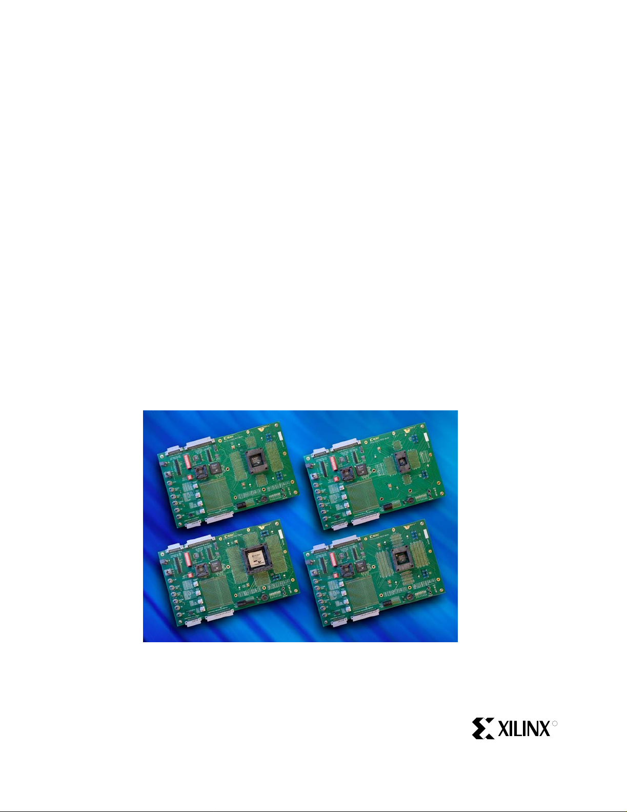
Virtex-II Prototype Platforms are prototype and demonstration boards that allow
designers to investigate and experiment with the features of Virtex-II series FPGAs. This
document describes the features and operation of the boards, including how to configure
chains of FPGAs and serial PROMs. Prototype Platforms are intended strictly for
evaluating the functionality of Virtex-II features and are not intended for A/C
characterization or high-speed I/O evaluation.
Features
• Independent power supply jacks for V
• Selectable V
• Configuration port for use with MultiLINX™ or Parallel Cable III cables
• Configuration mode switch
Virtex-II Prototype Platform www.xilinx.com 11
UG015 / PN0401974 (v1.1) January 14, 2003 1-800-255-7778
for each SelectIO™ bank
CCO
CCINT
, V
AUX
, and V
CCO

R
• Four global clock (GCLK) inputs
♦ two 50Ω SMB connectors
♦ two LVTTL-type oscillator sockets
• On-board programmable oscillator
• Selectable on-board clock frequency (from 25 MHz to 90 MHz)
• Power indicator LED
• 44-pin, VQFP PROM socket for any configuration mode
• JTAG port for reprogramming the XC17Vxx and XC18Vxx series reconfigurable
PROMs and the User FPGA (DUT)
• Upstream and downstream System ACE and Configuration Interface connectors
• On-board battery holder
The kit contains headers that can be soldered to the breakout area, if desired. These
headers are useful with certain types of oscilloscope probes for either connecting function
generators or wiring pins to the prototype area.
The Virtex-II Prototype Platform board (referred to as “the board”) contains two FPGAs, a
Device Under Test (DUT) FPGA and a Service FPGA.
The DUT can be configured either by a PROM in the User PROM socket or by the PROM
Daughter Card Interface header. The header allows the PROM to be substituted with a
daughter board, permitting daisy-chaining of PROMs and experimentation with other
configuration methods. (Consult the Xilinx data book,
http://www.xilinx.com/partinfo/databook.htm
, for selecting the appropriate PROM
device for each particular Virtex-II device.)
In addition to the User PROM socket and the PROM Daughter Card Interface header, there
are two upstream connectors and two downstream connectors. The upstream connectors
can be connected to configure the DUT using any configuration source, such as a
MultiLINX cable, Parallel Cable III, Parallel Cable IV, or System ACE. The downstream
connectors can be used to connect to another board in a chain.
The Service FPGA is a switch matrix used to control the routing of all of the configuration
signals on the board. This enables simple rotary switches (rather than jumpers) to control
the board, minimizing training and errors. An XC18V01 serial PROM configures the
Service FPGA. Neither this PROM nor the Service FPGA are part of the user configuration
chain. Only the DUT and its related configuration PROM are part of the configuration
chain.
Warning!
board to malfunction. This header is for internal use only.
Do not use the JTAG Interface Service PROM and FPGA header. This can cause the
12 www.xilinx.com Virtex-II Prototype Platform
1-800-255-7778 UG015 / PN0401974 (v1.1) January 14, 2003

Introduction
*1: JTAG Control
0: FPGA
1: PROM
2: FPGA→PROM
3: PROM→FPGA
4: FEEDTHROUGH
*2: Configuration Mode
0: MASTER SERIAL (PROM)
1: MASTER SERIAL (UPSTREAM)
2: MASTER SELECT MAP (PROM)
3: MASTER SELECT MAP (UPSTREAM)
4: SLAVE SERIAL
5: JTAG
6: SELECT MAP
7: EXTERNAL
Figure 1 shows a block diagram of the board.
HSWAP_EN (ON/OFF)
CLK_DOUBLE
Clock Enable Dip Switch
Clock
Generator
Frequency Select
25-90 MHz
JTAG Control *1
Configuration Mode *2
Chip Select
To Upstream Board
Select Map
JTAG
Service FPGA
JTAG Select Map
To Downstream Board
JTAG
TCK, TMS, TDI, TDO
Parallel/Serial
D0-D7, CCLK
Program
LVCMOS2 OSC LVCMOS2 OSC SMB
Data/Control
CCLK
JTAG
MODE
GCLK
User Reset
Header for PROM
Daughter Board
SPROM
(VQ44 Socket)
Virtex-II
DUT
VBATT
Done
LED
Test Points
on All Pins
Init
LED
R
Power Bus and Switches
LEDs
To Upstream Board
3.3V Jack
To Downstream Board
9V Jack
1.5V
3.3V
3.3V
3PDT
Switch
On-Off-On
VCCI
VCCO
VCC
Local Power
Figure 1: Virtex-II Prototype Platform Block Diagram
VCC Jack
VCCO Jack
VCCI Jack
UG015_01_052101
Virtex-II Prototype Platform www.xilinx.com 13
UG015 / PN0401974 (v1.1) January 14, 2003 1-800-255-7778
R
Detailed Description
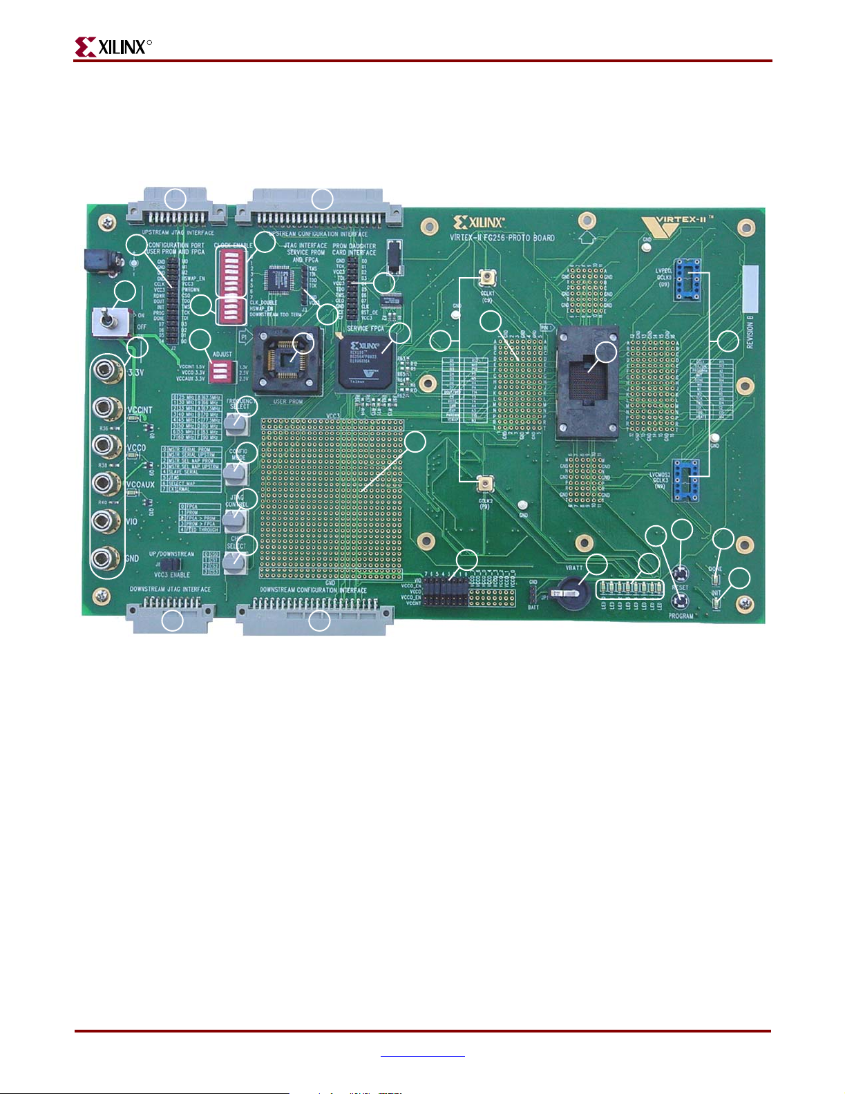
The Virtex-II Prototype Platform board is shown in Figure 2. Each feature is detailed in the
numbered sections that follow.
5a 5c
3
1
18
2
1a
5b 5d
17
10
9
11
8
4
5
6
7
16
12
13
20
14
19
21
22
23
15
24
25
Figure 2: Detailed Description of Virtex-II Prototype Platform Components
1. Power Switch
The board has an on-board power supply and a three-position power switch: upward on,
off, and downward on. When lit, a green LED indicates power to the device core when
V
Upward On Position
In the upward on position, the power switch enables delivery of all power to the board by
way of voltage regulators situated on the backside of the board. These regulators feed off
an external power brick with a voltage range from 5-14V. Special circuitry delivers the
required power to the Service FPGA and Service PROM.
The voltage regulators deliver fixed voltages; however, you can adjust these voltages by
changing the settings on the dip switch site marked ADJUST (1a) as shown in Figure 2.
Maximum current range for each supply is 500 mA.
14 www.xilinx.com Virtex-II Prototype Platform
is 1.5V or higher.
CCINT
1-800-255-7778 UG015 / PN0401974 (v1.1) January 14, 2003

Detailed Description
Off Position
Downward On Position
R
Table 1: Voltage Ranges
Label Max Voltage Min Voltage
VCCINT 1.5V 1.3V
VCCO 3.3V 2.5V
VCCAUX 3.3V 2.5V
In the off position, the power switch disables all modes of powering the DUT in standalone operation.
In the downward on position, the power switch enables delivery of all power from the six
power supply jacks.
2. Power Supply Jacks
In the downward on position, the power switch enables delivery of power to the board by
way of the power supply jacks. These six jacks are:
• 3.3V
♦ Supplies power to the on-board serial PROM, to the Service FPGA and its
supporting PROM, to the two oscillators, and to all pins marked V
board. This includes pins in the configuration port (user PROM and FPGA), the
prototyping area, and the V
• VCCINT
♦ Supplies voltage to the core of the DUT (Consult the Xilinx data book,
http://www.xilinx.com/partinfo/databook.htm
voltage for the device you are using)
• VCCO
♦ Supplies I/O voltages to the DUT
♦ Each can be powered from one of three sources (V
appropriate placement of jumpers on the header
• VCCAUX
♦ Supplies voltage to the V
• VIO
♦ Supplies voltage to the V
♦ Provides the option of an additional voltage source for the V
♦ Can be driven externally or from the board
• GND
enable jumpers
CC3
header and the V
AUX
header (not to the DUT)
IO
, for the maximum V
AUX
, V
CCO
DUT pins
CCINT
CCO
, or VIO) by
CC3
banks
on the
CCINT
Virtex-II Prototype Platform www.xilinx.com 15
UG015 / PN0401974 (v1.1) January 14, 2003 1-800-255-7778

R
3. Configuration Port User PROM and FPGA Header
This header is used to connect a MultiLINX cable or Parallel Cable III cable to the board
and supports all Virtex-II device configuration modes. (See Table 4 for connecting cables to
the Configuration Port User PROM and FPGA header.)
4. Frequency Select Switch
The frequency select switch sets the frequency of the on-board clock generator. One of
sixteen frequencies can be selected as shown in Table 2.
Table 2: Clock Generator Frequencies
Switch Position Clock Frequency Switch Position Clock Frequency
025 MHz862.5 MHz
130 MHz966 MHz
2 33 MHz A 67.5 MHz
340 MHzB70 MHz
4 45 MHz C 77.5 MHz
550 MHzD80 MHz
655 MHzE83 MHz
760 MHzF90 MHz
5. Configuration Mode Switch
The configuration mode switch determines the configuration mode of the DUT using the
options shown in Table 3.
Table 3: Configuration Mode Options
Switch Position Mode Label
0 MSTR SERIAL PROM
1 MSTR SERIAL UPSTRM
2 MSTR SEL MAP PROM
3 MSTR SEL MAP UPSTRM
4SLAVE SERIAL
5JTAG
6 SELECT MAP
7EXTERNAL
In master serial configuration modes, the DUT is configured from either the on-board
serial PROM, the Upstream Configuration Interface connector, or the Configuration Port
User PROM and FPGA header.
16 www.xilinx.com Virtex-II Prototype Platform
1-800-255-7778 UG015 / PN0401974 (v1.1) January 14, 2003

Detailed Description
Master Serial PROM Mode
Master Serial UPSTREAM Mode
In either of the master serial configuration modes, the CCLK and DIN (D0) signals are
routed to the Downstream Configuration Interface connector to allow daisy-chaining to
downstream slave serial devices.
Note:
stream.
Only one master se rial device is allowed in a chain and it must be the first FPGA devi ce in the
In master select map modes, the CCLK and D0-D7 signals are routed to the Downstream
Configuration Interface connector to allow daisy-chaining to downstream devices.
Note:
http://www.xilinx.com/partinfo/databook.htm
For more details on configuration modes, consult the Xilinx Data Book located at:
.
In switch position 0 (Master Serial PROM) the on-board PROM is used as the configuration
data source.
In switch position 1 (Master Serial UPSTREAM) the Upstream Configuration Interface
connector or the Configuration User PROM and FPGA header can be used as the
configuration data source. All configuration signals from/to the DUT are then routed
accordingly.
Table 4 shows the Configuration Port User PROM and FPGA header pins on the board and
the corresponding pins for connecting MultiLINX or Parallel Cable III cables for serial
mode.
R
Table 4: Serial Mode
Configuration Port User
PROM and FPGA Header
MultiLINX Pins Parallel Cable III Pins
VCC3 PWR VCC
GND GND GND
CCLK CCLK CCLK
DONE DONE D/P
D0 DIN DIN
PROG PROG PROG
INIT INIT
Master Select Map PROM Mode
In switch position 2 (Master Select Map PROM) the on-board PROM or PROM daughter
card interface is used as the configuration data source for the DUT. The PROM, the M0-
M2, CS, and the RW signals are set by the Service FPGA.
Master Select Map UPSTREAM Mode
In switch position 3 (Master Select Map UPSTREAM) the Upstream Configuration
Interface connector or the Configuration Port User PROM and FPGA header can be used as
a configuration data source for the DUT. All configuration signals from/to the DUT are
then routed accordingly. In this mode, the CCLK and D0-D7 are routed to the
Downstream Configuration Interface connector to allow daisy-chaining to downstream
Virtex-II Prototype Platform www.xilinx.com 17
UG015 / PN0401974 (v1.1) January 14, 2003 1-800-255-7778

R
devices. When configuring from the Upstream Configuration Interface connector, the M0M2, CS, and RW signals are set by the Upstream Configuration Interface connector or the
Configuration User PROM and FPGA header pins.
Table 5 shows the Configuration Port User PROM and FPGA header pins on the board and
the corresponding pins for connecting the MultiLINX cable for select map mode.
Table 5: Select Map Mode
Configuration Port User
PROM and FPGA Header
MultiLINX Pins
VCC3 PWR
GND GND
CCLK CCLK
DONE DONE
PROG PROG
INIT INIT
CS0 CS0 (CS)
RDWR RS (RDWR)
DOUT RDY/BUSY
D0 D0
D1 D1
D2 D2
D3 D3
D4 D4
D5 D5
D6 D6
D7 D7
Slave Serial Mode
In switch position 4 (Slave Serial) either the Upstream Configuration Interface connector or
the Configuration Port User PROM and FPGA header are used as a configuration data
source for configuring the DUT in slave serial format. In this mode, the upstream device
supplies the CCLK and DIN signals, as well as all other configuration signals to the DUT.
(See Table 4 for connecting to the Configuration Port User PROM and FPGA header.)
JTAG Mode
In switch position 5 (JTAG) the System ACE connectors to upstream and downstream
boards are selected. Each System ACE connector contains pins for each of the four JTAG
signals: TCK, TMS, TDI, and TDO.
TCK and TMS are parallel feedthrough connections from the upstream System ACE
connector to the downstream System ACE connector and drive the TCK and TMS pins of
18 www.xilinx.com Virtex-II Prototype Platform
1-800-255-7778 UG015 / PN0401974 (v1.1) January 14, 2003

Detailed Description
the on-board PROM and the DUT. TDI is a serial JTAG chain input and TDO is a serial
JTAG chain output.
Note:
The DOWNSTREAM_ TDO TERM switc h must be set t o the “o n” pos ition on the last b oard in
the chain to connect the TDO pin of the final device to the TDO feedback chain.
Table 6: JTAG Mode
R
Configuration Port User
PROM and FPGA Header
MultiLINX Pins Parallel Cable III Pins
VCC3 PWR VCC
GND GND GND
TMS TMS TMS
TDI TDI TDI
TDO RD (TDO) TDO
TCK TCK TCK
Select Map Mode
In switch position 6 (Select Map) the configuration data is supplied byte wide from the
Upstream Configuration Interface connector or from the Configuration Port User PROM
and FPGA Header and requires an external clock source. The mode pins M0-M2 are set by
the Service FPGA. The CS and RDWR signals are generated from the Upstream
Configuration Interface connector. (See Table 5 for connecting to the Configuration Port
User PROM and FPGA header.)
Configuration/Readback from the Upstream Connector
To use configuration/readback mode, you must set the configuration mode switch to
position 6 (Select Map). You must also set the chip select switch to provide each device in
the chain a unique ID. (See “7. Chip Select Switch”.)
In this mode of configuration, byte-wide data is obtained from the Upstream
Configuration Interface connector. The CS and RDWR pins are also supplied by the
Upstream Configuration Interface connector.
The RDWR pin on the Upstream Configuration Interface connector determines the data
direction. When RDWR is low, the data flows from the DUT to the Upstream
Configuration Interface connector.
The value of the INIT pin on the Upstream Configuration Interface connector will be the
value of the INIT pin on the DUT, AND’ed with the INIT pin from the Downstream
Configuration Interface connector. Therefore, INIT will only be high when all INIT pins in
the chain are high.
The value of the DONE pin on the Upstream Configuration Interface connector will be the
value of the DONE pin on the DUT, AND’ed with the DONE pin from the downstream
configuration connector. Therefore, DONE will only be high when all DONE pins in the
chain are high. There is a 330Ω pullup resistor on the DONE pin of the DUT.
External Mode
In switch position 7 (External) the external configuration mode places all connections from
the Service FPGA to the DUT in a high-impedance condition. In this mode, the prototype
board acts as a simple breakout board and all connections to the DUT (except for power)
Virtex-II Prototype Platform www.xilinx.com 19
UG015 / PN0401974 (v1.1) January 14, 2003 1-800-255-7778

R
must be provided by the user. The only services provided by the board in this mode are the
on-board oscillators, the DONE and INIT LEDs, and VBATT. All connections to the
configuration pins must be made using the breakout test points.
5a. Upstream System ACE Connector
The Upstream System ACE connector, as shown in Figure 3, can be used to configure the
DUT. This connector can be sourced by any JTAG configuration stream. For example, a
System ACE Controller with CompactFlash can be used to generate very large JTAG
streams for configuring multiple Virtex-II Prototype Platforms using the Downstream
System ACE connector.
UPSTREAM_TDO
GND
UPSTREAM_TCK
GND
V5
V5
V5
V5
V5
GND
Figure 3: Upstream System ACE Connector, 20-Pin Female
5b. Downstream System ACE Connector
The Downstream System ACE connector, as shown in Figure 4, is used to pass
configuration information to a DUT in a downstream prototype platform from sources
such as a MultiLINX cable, Parallel Cable III, or an Upstream System ACE connector.
GND
V5
V5
V5
V5
GND
UPSTREAM_TDI
GND
UPSTREAM_TMS
NC
135791113151719
2468101214161820
VCC3_EN
VCC3_EN
VCC3_EN
VCC3_EN
GND
GND
VCC3_EN
VCC3_EN
VCC3_EN
VCC3_EN
2468101214161820
UG015_03_061401
V5
GND
DOWNSTREAM_TCK
GND
DOWNSTREAM_TDO
135791113151719
NC
DOWNSTREAM_TMS
GND
DOWNSTREAM_TDI
GND
UG015_04_061401
Figure 4: Downstream System ACE Connector, 20-Pin Male
20 www.xilinx.com Virtex-II Prototype Platform
1-800-255-7778 UG015 / PN0401974 (v1.1) January 14, 2003

Detailed Description
5c. Upstream Configuration Interface Connector
R
The Upstream Configuration Interface connector, as shown in Figure 5, is used to
configure the DUT in select-map or slave-serial mode. This connector can only be sourced
by a the Downstream Configuration Interface connector of another prototype platform.
GND
GND
GND
GND
V5
V5
VCC3_EN
GND
VCC3_EN
VCC3_EN
VCC3_EN
UPSTREAM_TMS
UPSTREAM_TDI
UPSTREAM_TDO
UPSTREAM_TCK
V5
V5
UPSTREAM_PWRDWN
UPSTREAM_DOUT
UPSTREAM_INIT
UPSTREAM_PROG
UPSTREAM_RDWR
16 14 12 10 8 6 4 21820222426283032343638404244
15 13 11 9 7 5 3 11719212325272931333537394143
GND
GND
GND
UPSTREAM_HSWAP_EN
UPSTREAM_M2
UPSTREAM_M1
UPSTREAM_M0
UPSTREAM_CS3
UPSTREAM_CS2
UPSTREAM_CS1
UPSTREAM_CS0
UPSTREAM_D0
UPSTREAM_D1
UPSTREAM_D2
UPSTREAM_D3
UPSTREAM_D4
UPSTREAM_D5
UPSTREAM_D6
UPSTREAM_D7
UPSTREAM_DONE
UPSTREAM_CCLK
NC
Figure 5: Upstream Configuration Interface Connector, 44-Pin Female
UG015_05_051001
Virtex-II Prototype Platform www.xilinx.com 21
UG015 / PN0401974 (v1.1) January 14, 2003 1-800-255-7778

R
5d. Downstream Configuration Interface Connector
The Downstream Configuration Interface connector, as shown in Figure 6, passes selectmap or slave-serial configuration information to a DUT in a downstream prototype
platform from sources such as a MultiLINX cable or a Parallel Cable III.
DOWNSTREAM_RDWR
DOWNSTREAM_PROG
DOWNSTREAM_INIT
DOWNSTREAM_DOUT
DOWNSTREAM_PWRDWN
V5
V5
DOWNSTREAM_TCK
DOWNSTREAM_TDO
DOWNSTREAM_TDI
DOWNSTREAM_TMS
VCC3_EN
VCC3_EN
VCC3_EN
GND
VCC3_EN
V5
V5
GND
GND
GND
GND
Figure 6: Downstream Configuration Interface Connector, 44-Pin Male
NC
DOWNSTREAM_CCLK
DOWNSTREAM_DONE
DOWNSTREAM_D7
DOWNSTREAM_D6
DOWNSTREAM_D5
DOWNSTREAM_D4
DOWNSTREAM_D3
DOWNSTREAM_D2
DOWNSTREAM_D1
15 13 11 9 7 5 3 11719212325272931333537394143
16 14 12 10 8 6 4 21820222426283032343638404244
DOWNSTREAM_D0
DOWNSTREAM_CS0
DOWNSTREAM_CS1
DOWNSTREAM_CS2
DOWNSTREAM_CS3
DOWNSTREAM_M0
DOWNSTREAM_M1
DOWNSTREAM_M2
DOWNSTREAM_HSWAP_EN
GND
GND
GND
UG015_06_051001
6. JTAG Control Switch
The JTAG control switch is functional only when the configuration mode switch is set to
JTAG (position 5). The JTAG control switch is used to select the order of the devices in the
JTAG chain using the options shown in Table 7.
Table 7: JTAG Control Options
Switch Number Mode Description
0 DUT DUT only in chain
1 PROM User PROM only in chain
2DUT → PROM DUT first, PROM second in chain
3PROM → DUT PROM first, DUT second in chain
4 Feedthrough Allows a board to be switched out of the JTAG
Note:
1. The Service FPGA and its supporting Service PROM are not part of the JTAG chain.
2. Since all of the JTAG signals are routed in and out of the Service FPGA multiple times, use
caution to not run the JTAG bus too fast.
chain without physically removing it
22 www.xilinx.com Virtex-II Prototype Platform
1-800-255-7778 UG015 / PN0401974 (v1.1) January 14, 2003

Detailed Description
7. Chip Select Switch
8. User PROM Socket
The chip select switch assigns a unique identification (ID) to each DUT in a select map
configuration chain. This switch may be set from 0 to 3, allowing up to four devices to be
configured/read back in a select map chain. During readback, each board in the chain
must have a unique ID, otherwise more than one device will drive the data bus. However,
multiple DUTs may be set to the same ID for “Select Map Mode” configuration. Pins on the
configuration connectors correspond to each ID. The CS pin on the DUT will be connected
to the CS pin on the configuration connector that corresponds to its chip select switch.
The CS pin on the DUT is set to zero, by default, when the configuration mode is set to
Master Select Map PROM. Otherwise, its value is dependent on the value of the
UPSTREAM_CS[3:0] pins.
The user PROM socket can be used to configure the Virtex-II device in master serial mode.
The socket accepts XC17V01-V04 and XC18V01-V04 series configuration PROMs in VQ44
packages. The PROM port can also be used to reprogram the PROM using JTAG. (Consult
the Xilinx data book, http://www.xilinx.com/partinfo/databook.htm
appropriate PROM device for each particular Virtex-II device.)
, for selecting the
R
9. JTAG Interface, Service PROM, and FPGA Header
In addition to the user PROM, the board has a dedicated XC18V01 serial PROM that
configures the Service FPGA. The Service PROM and the Service FPGA are not part of the
user configuration chain. Only the DUT and its related configuration PROM are part of the
configuration chain.
Warning!
board to malfunction. This header is for internal use only.
Do not use the JTAG Interface Service PROM and FPGA header. This can cause the
10. PROM Daughter Card Interface
This header is located near the User PROM socket so that the PROM may be substituted
with a daughter board, permitting daisy-chaining of PROMs and experimentation with
other configuration methods.
Note:
PROM substitution is dependent upon configuration and JTAG switch settings.
11. Service FPGA
In addition to the DUT FPGA, the board contains a Service FPGA. The Service FPGA acts
as a switch matrix to control the routing of all of the configuration signals on the board.
This enables simple rotary switches (rather than jumpers) to control the board, minimizing
training and errors. The Service FPGA is configured by a dedicated Service PROM. The
Service FPGA and the Service PROM are not part of the user configuration chain. Only the
DUT and its related configuration PROM are part of the configuration chain.
Warning!
board to malfunction. This header is for internal use only.
Do not use the JTAG Interface Service PROM and FPGA header. This can cause the
Virtex-II Prototype Platform www.xilinx.com 23
UG015 / PN0401974 (v1.1) January 14, 2003 1-800-255-7778

R
12. Prototyping Area
The prototyping area accommodates 0.10" spaced ICs. The kit contains headers that can be
soldered to the breakout area, if desired. Power and ground buses are located at the top
and bottom, respectively, of the prototyping area.
13. V
Supply Jumpers
CCO
Virtex-II series devices have eight SelectIO banks, labeled 0 through 7, each with a V
supply. VCCO_EN supply jumpers can connect each bank to one of the three on-board
supplies, V
Virtex-II device to function normally.
CCINT
14. VBATT
An on-board battery holder is connected to the VBATT pin of the DUT. If an external
power s upply is used, the associated jumper must be removed. Select a 12 mm lithium coin
battery (3V), such as part numbers BR1216, CR1216, and BR1225 from Panasonic or any
other appropriate 12 mm lithium coin battery (3V).
15. Oscillator Sockets
The prototype board has two crystal oscillator sockets, both wired for standard LVTTLtype oscillators. These sockets connect to the DUT clock pads as shown in Table 8. On-
board termination resistors can be changed by the user. The oscillator sockets accept both
half- and full-sized oscillators and are powered by the 3.3V power supply.
Table 8: OSC Clock Pin Connections
FG256 FG456 FG676 FF1152
Label
Clock
Name
Number
, V
Pin
, or externally from VIO. These jumpers must be installed for the
CCO
Clock
Name
Pin
Number
Clock
Name
Pin
Number
Clock
Name
CCO
Pin
Number
OSC Socket Top GCLK0S D9 GCLK0S D12 GCLK0S F14 GCLK7P K18
OSC Socket Bottom GCLK3S N9 GCLK3S W12 GCLK3S AA14 GCLK4P AF18
16. Function Generator Clock Inputs
In addition to the oscillator sockets, there are two 50Ω SMB connectors that allow
connection to an external function generator. These connect to the DUT clock pads as
shown in Table 9.
Table 9: SMB Clock Pin Connections
FG256 FG456 FG676 FF1152
Label
SMB Top GCLK1P C9 GCLK1P E12 GCLK1P G14 GCLK6S J18
SMB Bottom GCLK2P P9 GCLK2P Y12 GCLK2P AB14 GCLK5S AG18
Clock
Name
Pin
Number
Clock
Name
Pin
Number
Clock
Name
Pin
Number
Clock
Name
Number
Pin
24 www.xilinx.com Virtex-II Prototype Platform
1-800-255-7778 UG015 / PN0401974 (v1.1) January 14, 2003

Detailed Description
17. Clock Enable Switches 0-7
The user has access to eight additional global clocks on the DUT. These clocks can be
enabled by setting the appropriate dip switches shown in Table 10. After selecting the
clock frequency, all enabled clocks run at that frequency.
Table 10: Dip Switches and Associated Global Clocks
FG256 FG456 FG676 FF1152
R
Label
Clock
Name
Pin
Number
Clock
Name
Pin
Number
Clock
Name
Pin
Number
Clock
Name
Pin
Number
CLOCK ENABLE 0 GCLK1S R9 GCLK1S AA12 GCLK1S AC14 GCLK6P AK19
CLOCK ENABLE 1 GCLK6P R8 GCLK6P Y11 GCLK6P AB13 GCLK1S AK16
CLOCK ENABLE 2 GCLK5S P8 GCLK5S W11 GCLK5S AA13 GCLK2P AG17
CLOCK ENABLE 3 GCLK4P N8 GCLK4P V11 GCLK4P Y13 GCLK3S AF17
CLOCK ENABLE 4 GCLK7P D8 GCLK7P D11 GCLK7P F13 GCLK0S H16
CLOCK ENABLE 5 GCLK6S C8 GCLK6S C11 GCLK6S E13 GCLK1P H17
CLOCK ENABLE 6 GCLK5P B8 GCLK5P B11 GCLK5P D13 GCLK2S E16
CLOCK ENABLE 7 GCLK2S B9 GCLK2S F13 GCLK2S H15 GCLK5P E19
The frequency of each of these clocks can be doubled by setting the CLK_DOUBLE switch,
shown in Table 11. Clock doubling is achieved by the DLL in the Service FPGA. However,
setting this switch doubles the frequency of all enabled clocks.
The remaining four FPGA global clocks are accessible through the header pins
surrounding the DUT.
Note:
1. When LED 7 is lighted before configuration, it implies that the DLL is locked.
2. The above 12 global clocks are not available through the breakout area test points.
18. Clock Enable Switches 8-12
The remaining four clock enable switches are described in Table 11.
Table 11: Dip Switches 8-12
Label Function
CLK_DOUBLE Doubles the frequency of all enabled clocks
HSWAP_EN Controls user I/O pullups before configuration
DOWNSTREAM_TDO_TERM Connects TDO of last device back to the feedback
chain
(not used)
Note:
For more information about HSWAP, see the Xilinx Data Book available at:
http://www.xilinx.com/partinfo/databook.htm.
Virtex-II Prototype Platform www.xilinx.com 25
UG015 / PN0401974 (v1.1) January 14, 2003 1-800-255-7778

R
19. DUT Socket
The DUT socket contains the user FPGA, referred to as the Device Under Test.
The device must be oriented using the P1 indicator on the board. Failure to insert the
device to the proper orientation can damage the device. To avoid pin damage, always use
the vacuum tool provided when inserting or removing the Virtex-II device. When using
BGA packages, do not apply pressure to the device while activating the vacuum tool lever.
Doing so can damage the socket and/or the device.
20. Pin Breakout
The pin breakout area is used to monitor or apply signals to each of the DUT pins. Headers
can be soldered to the breakout area to use with certain types of oscilloscope probes, for
either connecting function generators or wiring pins to the pin breakout area. Clocks in the
pin breakout area that connect to the DUT clock pads are shown in Table 12.
Table 12: Breakout Clock Pin Connections
FG256 FG456 FG676 FF1152
Label
Breakout Area 1 GCLK3P A9 GCLK3P F12 GCLK3P H14 GCLK4S E18
Breakout Area 2 GCLK4S A8 GCLK4S A11 GCLK4S C13 GCLK3P E17
Breakout Area 3 GCLK7S T8 GCLK7S AA11 GCLK7S AC13 GCLK7S AK18
Breakout Area 4 GCLK0P T9 GCLK0PAB12 GCLK0PAD14 GCLK0PAK17
Clock
Name
Pin
Number
Clock
Name
Pin
Number
Clock
Name
Pin
Number
Clock
Name
Pin
Number
21. User LEDs (Active-High)
There are eight active-high user LEDs on the board. Before configuration, the LEDs reflect
the status of the configuration mode switch. During configuration, the LEDs are in a highimpedance condition. After configuration, the LEDs are available to the user and reflect the
status of pins D0-D7 (corresponding to LED 0-LED 7). The LED assignments are shown in
Table 13.
Table 13: LED Assignments and Corresponding I/O
Configuration Mode Status Pin Number For Package Type
LED
LED 0 Master Serial PROM Available as user
Before and During
Configuration
After
Configuration
LEDs
Status Pin FG256 FG456 FG676 FF1152
D0 P13 V18 Y20 AG10
LED 1 Master Serial UPSTREAM D1 R13 V17 Y19 AH11
LED 2 Master Select MAP PROM D2 N12 W18 AA20 AK7
LED 3 Master Select Map
UPSTREAM
LED 4 Slave Serial D4 P5 Y5 AB7 AK28
LED 5 JTAG D5 N5 W5 AA7 AL29
26 www.xilinx.com Virtex-II Prototype Platform
1-800-255-7778 UG015 / PN0401974 (v1.1) January 14, 2003
D3 P12 Y18 AB20 AK8

Detailed Description
Table 13: LED Assignments and Corresponding I/O (Continued)
Configuration Mode Status Pin Number For Package Type
R
LED
LED 6 Select Map D6 R4 AB4 AD6 AG24
LED 7 DLL Locked Status D7 P4 AA4 AC6 AG25
Before and During
Configuration
After
Configuration
Status Pin FG256 FG456 FG676 FF1152
22. Program Switch
The active-low program switch, when pressed, grounds the program pin on the DUT. This
switch is driven indirectly by the Service FPGA.
23. Reset Switch (Active-Low)
The reset switch connects (indirectly through the Service FPGA) to the INIT pin on the
DUT, allowing the user, after configuration, to reset the logic within the DUT. Before and
during configuration of the DUT, the INIT pin has no function. After configuration, the
INIT pin becomes a regular I/O. When pressed, this switch grounds the INIT pin.
24. DONE LED
The DONE LED indicates the status of the DONE pin on the DUT. This LED lights when
DONE is high or if power is applied to the board without a part in the socket.
25. INIT LED
The INIT LED lights during initialization.
Virtex-II Prototype Platform www.xilinx.com 27
UG015 / PN0401974 (v1.1) January 14, 2003 1-800-255-7778

R
User Programmable Pins
Table 14 shows the user hardware that corresponds to available DUT package types.
Table 14: User Hardware and Corresponding I/Os
Label FG256 FG456 FG676 FF1152
RESET (INIT) T13 AA19 AC21 AL5
D0/LED 0 P13 V18 Y20 AG10
D1/LED 1 R13 V17 Y19 AH11
D2/LED 2 N12 W18 AA20 AK7
D3/LED 3 P12 Y18 AB20 AK8
D4/LED 4 P5 Y5 AB7 AK28
D5/LED 5 N5 W5 AA7 AL29
D6/LED 6 R4 AB4 AD6 AG24
Pin Number For Package Type
D7/LED 7 P4 AA4 AC6 AG25
Note: Refer to the readme.txt file for implementation of these user pins.
Table 15 shows the clock pins and corresponding I/Os.
Table 15: Clock Pins and Corresponding I/Os
FG256 FG456 FG676 FF1152
Clock Pins
Clock
Name
Pin
Number
Clock
Name
Pin
Number
Clock
Name
Pin
Number
Clock
Name
Number
CLOCK ENABLE 0 GCLK1S R9 GCLK1S AA12 GCLK1S AC14 GCLK6P AK19
CLOCK ENABLE 1 GCLK6P R8 GCLK6P Y11 GCLK6P AB13 GCLK1S AK16
CLOCK ENABLE 2 GCLK5S P8 GCLK5S W11 GCLK5S AA13 GCLK2P AG17
CLOCK ENABLE 3 GCLK4P N8 GCLK4P V11 GCLK4P Y13 GCLK3S AF17
CLOCK ENABLE 4 GCLK7P D8 GCLK7P D11 GCLK7P F13 GCLK0S H16
CLOCK ENABLE 5 GCLK6S C8 GCLK6S C11 GCLK6S E13 GCLK1P H17
CLOCK ENABLE 6 GCLK5P B8 GCLK5P B11 GCLK5P D13 GCLK2S E16
CLOCK ENABLE 7 GCLK2S B9 GCLK2S F13 GCLK2S H15 GCLK5P E19
OSC Socket Top GCLK0S D9 GCLK0S D12 GCLK0S F14 GCLK7P K18
Pin
OSC Socket Bottom GCLK3S N9 GCLK3S W12 GCLK3S AA14 GCLK4P AF18
SMB Top GCLK1P C9 GCLK1P E12 GCLK1P G14 GCLK6S J18
SMB Bottom GCLK2P P9 GCLK2P Y12 GCLK2P AB14 GCLK5S AG18
Breakout Area 1 GCLK3P A9 GCLK3P F12 GCLK3P H14 GCLK4S E18
Breakout Area 2 GCLK4S A8 GCLK4S A11 GCLK4S C13 GCLK3P E17
28 www.xilinx.com Virtex-II Prototype Platform
1-800-255-7778 UG015 / PN0401974 (v1.1) January 14, 2003

User Programmable Pins
Table 15: Clock Pins and Corresponding I/Os (Continued)
FG256 FG456 FG676 FF1152
R
Clock Pins
Clock
Name
Pin
Number
Clock
Name
Pin
Number
Clock
Name
Pin
Number
Clock
Name
Pin
Number
Breakout Area 3 GCLK7S T8 GCLK7S AA11 GCLK7S AC13 GCLK7S AK18
Breakout Area 4 GCLK0P T9 GCLK0PAB12 GCLK0PAD14 GCLK0PAK17
Virtex-II Prototype Platform www.xilinx.com 29
UG015 / PN0401974 (v1.1) January 14, 2003 1-800-255-7778
 Loading...