


R
LogiCORE™ IP
Initiator/Target
v5.1 for PCI-X™
Getting Started Guide
UG158 March 24, 2008
Xilinx is disclosing this Document and Intellectual Property (hereinafter “the Design”) to you for use in the development of designs
R
to operate on, or interface with Xilinx FPGAs. Except as stated herein, none of the Design may be copied, reproduced,
distributed, republished, downloaded, displayed, posted, or transmitted in any form or by any means including, but not limited to,
electronic, mechanical, photocopying, recording, or otherwise, without the prior written consent of Xilinx. Any unauthorized use
of the Design may violate copyright laws, trademark laws, the laws of privacy and publicity, and communications regulations and
statutes.
Xilinx does not assume any liability arising out of the application or use of the Design; nor does Xilinx convey any license under
its patents, copyrights, or any rights of others. You are responsible for obtaining any rights you may require for your use or
implementation of the Design. Xilinx reserves the right to make changes, at any time, to the Design as deemed desirable in the
sole discretion of Xilinx. Xilinx assumes no obligation to correct any errors contained herein or to advise you of any correction if
such be made. Xilinx will not assume any liability for the accuracy or correctness of any engineering or technical support or
assistance provided to you in connection with the Design.
THE DESIGN IS PROVIDED “AS IS" WITH ALL FAULTS, AND THE ENTIRE RISK AS TO ITS FUNCTION AND
IMPLEMENTATION IS WITH YOU. YOU ACKNOWLEDGE AND AGREE THAT YOU HAVE NOT RELIED ON ANY ORAL OR
WRITTEN INFORMATION OR ADVICE, WHETHER GIVEN BY XILINX, OR ITS AGENTS OR EMPLOYEES. XILINX MAKES
NO OTHER WARRANTIES, WHETHER EXPRESS, IMPLIED, OR STATUTORY, REGARDING THE DESIGN, INCLUDING ANY
WARRANTIES OF MERCHANTABILITY, FITNESS FOR A PARTICULAR PURPOSE, TITLE, AND NONINFRINGEMENT OF
THIRD-PARTY RIGHTS.
IN NO EVENT WILL XILINX BE LIABLE FOR ANY CONSEQUENTIAL, INDIRECT, EXEMPLARY, SPECIAL, OR INCIDENTAL
DAMAGES, INCLUDING ANY LOST DATA AND LOST PROFITS, ARISING FROM OR RELATING TO YOUR USE OF THE
DESIGN, EVEN IF YOU HAVE BEEN ADVISED OF THE POSSIBILITY OF SUCH DAMAGES. THE TOTAL CUMULATIVE
LIABILITY OF XILINX IN CONNECTION WITH YOUR USE OF THE DESIGN, WHETHER IN CONTRACT OR TORT OR
OTHERWISE, WILL IN NO EVENT EXCEED THE AMOUNT OF FEES PAID BY YOU TO XILINX HEREUNDER FOR USE OF
THE DESIGN. YOU ACKNOWLEDGE THAT THE FEES, IF ANY, REFLECT THE ALLOCATION OF RISK SET FORTH IN THIS
AGREEMENT AND THAT XILINX WOULD NOT MAKE AVAILABLE THE DESIGN TO YOU WITHOUT THESE LIMITATIONS OF
LIABILITY.
The Design is not designed or intended for use in the development of on-line control equipment in hazardous environments
requiring fail-safe controls, such as in the operation of nuclear facilities, aircraft navigation or communications systems, air traffic
control, life support, or weapons systems (“High-Risk Applications”). Xilinx specifically disclaims any express or implied
warranties of fitness for such High-Risk Applications. You represent that use of the Design in such High-Risk Applications is fully
at your risk.
© 2000-2008 Xilinx, Inc. All rights reserved. XILINX, the Xilinx logo, and other designated brands included herein are trademarks
of Xilinx, Inc. All other trademarks are the property of their respective owners.
PCI-X v5.1 165 Getting Started Guide
UG158 March 24, 2008
The following table shows the revision history for this document.
Version Revision
06/01/00 1.0 Initial Xilinx release.
06/15/00 1.1 Accumulated miscellaneous updates and bug fixes.
07/26/00 1.2 Accumulated miscellaneous updates and bug fixes.
08/28/00 1.3 Fine tuning of text frame and paragraph format spacings.
04/11/01 2.0 Revised formats to take advantage of FrameMaker 6.0 book features.
05/02/01 2.1 Master page changes.
07/11/01 2.2 Accumulated miscellaneous updates and bug fixes.
PCI-X v5.1 165 Getting Started Guide www.xilinx.com
UG158 March 24, 2008

Version Revision
04/04/02 2.2.1 Updated trademarks page in ug000_title.fm.
06/24/02 3.0 Initial Xilinx release of corporate-wide common template set, used for User Guides,
Tutorials, Release Notes, Manuals, and other lengthy, multiple-chapter documents
created by both CMP and ITP. See related documents for further information.
Descriptions for revisions prior to v3.0 have been abbreviated. For a full summary of revision
changes prior to v3.0, refer to v2.2.1 template set.
10/30/02 3.1 Updated spelling of RocketIO and SelectIO trademarks in ug000_title.fm per 10/09/02
broadcast email announcement. Also updated file version number and date.
12/06/02 3.2 Fixed all instances of old character formats in header/footer in Master pages.
01/20/03 3.3 Revised copyright date in ug000_title.fm to 2003. Changed all instances of “Manual” in
ug000_preface.fm to “Guide.”
02/06/03 3.4 Added paragraph formats GlossBulleted, GlossNumbered, and GlossNumberedCont.
02/25/03 3.4.1 Minor clean-ups and corrections.
03/25/03 3.5 • Corrected Reference Page identification problem that prevented the IX (index)
Reference page from taking control of Index formatting.
• Modified paragraph tags Level1IX through Level3IX (index entries) to provide a
more uniform appearance and enhance clarity.
• Removed <Italic> attribute from Heading2TOC special string on Reference pages.
• Changed autonumbering properties of FigureTitle and TableTitle to remove chapter
number and hyphen.
04/30/03 3.5.1 Updated Additional Resources table in Preface to give correct URL to data sheets index
page instead of to obsolete Programmable Logic Data Book page.
11/11/04 3.5.2 Added installation and licensing chapter; updated to current template.
12/1/04 3.6 Virtex-4 updates; addition of information to Family Specific Considerations, Chapter 3.
3/7/05 3.7 Updated to system 7.1i and build 5.0.95
5/13/05 4.0 Updated to build 5.0.100 and Xilinx tools 7.1i SP2.
8/31/05 5.0 Updated to build 5.0.101 and Xilinx tools 7.1i SP3.
9/12/05 6.0 Updated to build 5.0.102, Xilinx tools 7.1i to SP4, changed release date, removed
instruction to confirm directory structure from Core Licensing chapter.
1/18/06 7.0 Updated build to 5.0.105, Xilinx tools to 8.1i, release date, licensing chapter.
2/14/06 7.5 Advanced build to 108, added SP2 support to ISE v8.1i, updated release date.
7/13/06 8.0 Advanced build to 160, ISE to v8.21, release date
2/15/07 8.1 Advanced build to 161, release date, minor updates
5/17/07 9.0 Changed title and text references to PCI-X and PCI to comply with PCI-SIG trademark
guidelines. Advanced build to 162, support for IUS to v5.7.
8/08/07 9.1 Updated for IP1 Jade Minor release. Changed capacitor value to 10 uF to match XAPP653
recommendation.
www.xilinx.com PCI-X v5.1 165 Getting Started Guide
UG158 March 24, 2008

Version Revision
10/10/07 9.5 Updated for IP2 Jade Minor release. Added section regarding configuration pins to
device family chapter.
3/24/08 10.0 Updated tools for IP0K release.
PCI-X v5.1 165 Getting Started Guide www.xilinx.com
UG158 March 24, 2008

Table of Contents
Schedule of Figures. . . . . . . . . . . . . . . . . . . . . . . . . . . . . . . . . . . . . . . . . . . . . . . . . . . . . . . . . . 7
Preface: About This Guide
Guide Contents. . . . . . . . . . . . . . . . . . . . . . . . . . . . . . . . . . . . . . . . . . . . . . . . . . . . . . . . . . . . . . 9
Conventions . . . . . . . . . . . . . . . . . . . . . . . . . . . . . . . . . . . . . . . . . . . . . . . . . . . . . . . . . . . . . . . . 10
Typographical. . . . . . . . . . . . . . . . . . . . . . . . . . . . . . . . . . . . . . . . . . . . . . . . . . . . . . . . . . . . 10
Online Document . . . . . . . . . . . . . . . . . . . . . . . . . . . . . . . . . . . . . . . . . . . . . . . . . . . . . . . . . 11
Chapter 1: Getting Started
System Requirements . . . . . . . . . . . . . . . . . . . . . . . . . . . . . . . . . . . . . . . . . . . . . . . . . . . . . . 13
About the Example Design . . . . . . . . . . . . . . . . . . . . . . . . . . . . . . . . . . . . . . . . . . . . . . . . . 13
Additional Documentation. . . . . . . . . . . . . . . . . . . . . . . . . . . . . . . . . . . . . . . . . . . . . . . . . . 14
Technical Support . . . . . . . . . . . . . . . . . . . . . . . . . . . . . . . . . . . . . . . . . . . . . . . . . . . . . . . . . . 14
Feedback . . . . . . . . . . . . . . . . . . . . . . . . . . . . . . . . . . . . . . . . . . . . . . . . . . . . . . . . . . . . . . . . . . . 14
Core Interface for PCI-X . . . . . . . . . . . . . . . . . . . . . . . . . . . . . . . . . . . . . . . . . . . . . . . . . . . 14
Document . . . . . . . . . . . . . . . . . . . . . . . . . . . . . . . . . . . . . . . . . . . . . . . . . . . . . . . . . . . . . . . 14
Chapter 2: Licensing the Core
Before you Begin . . . . . . . . . . . . . . . . . . . . . . . . . . . . . . . . . . . . . . . . . . . . . . . . . . . . . . . . . . . 15
Licensing Options . . . . . . . . . . . . . . . . . . . . . . . . . . . . . . . . . . . . . . . . . . . . . . . . . . . . . . . . . . 15
Full System Hardware Evaluation . . . . . . . . . . . . . . . . . . . . . . . . . . . . . . . . . . . . . . . . . . 15
Full License . . . . . . . . . . . . . . . . . . . . . . . . . . . . . . . . . . . . . . . . . . . . . . . . . . . . . . . . . . . . . . 16
Direct Download . . . . . . . . . . . . . . . . . . . . . . . . . . . . . . . . . . . . . . . . . . . . . . . . . . . . . . . . . 16
Installing Your License File . . . . . . . . . . . . . . . . . . . . . . . . . . . . . . . . . . . . . . . . . . . . . . . . . 16
Chapter 3: Family Specific Considerations
Design Support. . . . . . . . . . . . . . . . . . . . . . . . . . . . . . . . . . . . . . . . . . . . . . . . . . . . . . . . . . . . . 17
Device Initialization. . . . . . . . . . . . . . . . . . . . . . . . . . . . . . . . . . . . . . . . . . . . . . . . . . . . . . . . . 21
Configuration Pins . . . . . . . . . . . . . . . . . . . . . . . . . . . . . . . . . . . . . . . . . . . . . . . . . . . . . . . . . 21
Bus Width Detection. . . . . . . . . . . . . . . . . . . . . . . . . . . . . . . . . . . . . . . . . . . . . . . . . . . . . . . . 21
Bus Mode Detection . . . . . . . . . . . . . . . . . . . . . . . . . . . . . . . . . . . . . . . . . . . . . . . . . . . . . . . . 21
Bus Clock Usage . . . . . . . . . . . . . . . . . . . . . . . . . . . . . . . . . . . . . . . . . . . . . . . . . . . . . . . . . . . 22
Electrical Compliance . . . . . . . . . . . . . . . . . . . . . . . . . . . . . . . . . . . . . . . . . . . . . . . . . . . . . . 23
Input Delay Buffers . . . . . . . . . . . . . . . . . . . . . . . . . . . . . . . . . . . . . . . . . . . . . . . . . . . . . . . . . 24
Generating Bitstreams. . . . . . . . . . . . . . . . . . . . . . . . . . . . . . . . . . . . . . . . . . . . . . . . . . . . . . 25
Chapter 4: Functional Simulation
Cadence IUS. . . . . . . . . . . . . . . . . . . . . . . . . . . . . . . . . . . . . . . . . . . . . . . . . . . . . . . . . . . . . . . . 27
Mentor Graphics ModelSim. . . . . . . . . . . . . . . . . . . . . . . . . . . . . . . . . . . . . . . . . . . . . . . . . 28
Verilog . . . . . . . . . . . . . . . . . . . . . . . . . . . . . . . . . . . . . . . . . . . . . . . . . . . . . . . . . . . . . . . . . . 28
VHDL . . . . . . . . . . . . . . . . . . . . . . . . . . . . . . . . . . . . . . . . . . . . . . . . . . . . . . . . . . . . . . . . . . . 29
Chapter 5: Synthesizing a Design
Synplicity Synplify. . . . . . . . . . . . . . . . . . . . . . . . . . . . . . . . . . . . . . . . . . . . . . . . . . . . . . . . . . 31
www.xilinx.com PCI-X v5.1 165 Getting Started Guide
UG158 March 24, 2008

Verilog . . . . . . . . . . . . . . . . . . . . . . . . . . . . . . . . . . . . . . . . . . . . . . . . . . . . . . . . . . . . . . . . . . 31
VHDL . . . . . . . . . . . . . . . . . . . . . . . . . . . . . . . . . . . . . . . . . . . . . . . . . . . . . . . . . . . . . . . . . . . 36
Exemplar LeonardoSpectrum . . . . . . . . . . . . . . . . . . . . . . . . . . . . . . . . . . . . . . . . . . . . . . 40
Xilinx XST . . . . . . . . . . . . . . . . . . . . . . . . . . . . . . . . . . . . . . . . . . . . . . . . . . . . . . . . . . . . . . . . . . 41
Chapter 6: Implementing a Design
ISE Foundation . . . . . . . . . . . . . . . . . . . . . . . . . . . . . . . . . . . . . . . . . . . . . . . . . . . . . . . . . . . . . 43
Chapter 7: Timing Simulation
Cadence IUS. . . . . . . . . . . . . . . . . . . . . . . . . . . . . . . . . . . . . . . . . . . . . . . . . . . . . . . . . . . . . . . . 45
Mentor Graphics ModelSim. . . . . . . . . . . . . . . . . . . . . . . . . . . . . . . . . . . . . . . . . . . . . . . . . 46
Verilog . . . . . . . . . . . . . . . . . . . . . . . . . . . . . . . . . . . . . . . . . . . . . . . . . . . . . . . . . . . . . . . . . . 46
VHDL . . . . . . . . . . . . . . . . . . . . . . . . . . . . . . . . . . . . . . . . . . . . . . . . . . . . . . . . . . . . . . . . . . . 46
PCI-X v5.1 165 Getting Started Guide www.xilinx.com
UG158 March 24, 2008

Schedule of Figures
Chapter 1: Getting Started
Chapter 2: Licensing the Core
Chapter 3: Family Specific Considerations
Figure 3-1: PCI/PCI-X Output Driver VCCO Generation . . . . . . . . . . . . . . . . . . . . . . . . . . . 23
Chapter 4: Functional Simulation
Chapter 5: Synthesizing a Design
Figure 5-1: Create a New Project . . . . . . . . . . . . . . . . . . . . . . . . . . . . . . . . . . . . . . . . . . . . . . . 31
Figure 5-2: Main Project Window . . . . . . . . . . . . . . . . . . . . . . . . . . . . . . . . . . . . . . . . . . . . . . . 32
Figure 5-3: Files to Add (Virtex Library) . . . . . . . . . . . . . . . . . . . . . . . . . . . . . . . . . . . . . . . . . 33
Figure 5-4: Files to Add (LogiCORE Files). . . . . . . . . . . . . . . . . . . . . . . . . . . . . . . . . . . . . . . 33
Figure 5-5: Files to Add (User Application) . . . . . . . . . . . . . . . . . . . . . . . . . . . . . . . . . . . . . . 34
Figure 5-6: Source Files in Main Project Window . . . . . . . . . . . . . . . . . . . . . . . . . . . . . . . . 34
Figure 5-7: Options for Implementation: Device . . . . . . . . . . . . . . . . . . . . . . . . . . . . . . . . . 35
Figure 5-8: Options for Implementation: Options/Constraints. . . . . . . . . . . . . . . . . . . . . 35
Figure 5-9: Create a New Project . . . . . . . . . . . . . . . . . . . . . . . . . . . . . . . . . . . . . . . . . . . . . . . 36
Figure 5-10: Main Project Window . . . . . . . . . . . . . . . . . . . . . . . . . . . . . . . . . . . . . . . . . . . . . . 37
Figure 5-11: Files to Add (Virtex Library) . . . . . . . . . . . . . . . . . . . . . . . . . . . . . . . . . . . . . . . . 37
Figure 5-12: Files to Add (LogiCORE Files). . . . . . . . . . . . . . . . . . . . . . . . . . . . . . . . . . . . . . 38
Figure 5-13: Files to Add (User Application) . . . . . . . . . . . . . . . . . . . . . . . . . . . . . . . . . . . . . 38
Figure 5-14: Main Project Window . . . . . . . . . . . . . . . . . . . . . . . . . . . . . . . . . . . . . . . . . . . . . . 39
Figure 5-15: Options for Implementation: Device . . . . . . . . . . . . . . . . . . . . . . . . . . . . . . . . 40
Chapter 6: Implementing a Design
Chapter 7: Timing Simulation
www.xilinx.com PCI-X v5.1 165 Getting Started Guide
UG158 March 24, 2008

PCI-X v5.1 165 Getting Started Guide www.xilinx.com
UG158 March 24, 2008

R
About This Guide
The Initiator/Target v5.1 for PCI-X Getting Started Guide provides information about the
LogiCORE™ IP interface core for Peripheral Component Interconnect Extended (PCI-X),
which provides a fully verified, pre-implemented PCI-X bus interface targeting devices
based on the Virtex™ FPGA architecture.
The guide also includes an example design in both Verilog-HDL and VHDL that lets you
simulate, synthesize, and implement the interface to understand the design flow for PCI-X.
Guide Contents
This manual contains the following chapters:
• Chapter 1, “Getting Started,”describes the Initiator/Target core for PCI-X and
provides information about getting technical support, and providing feedback to
Xilinx about the core and the accompanying documentation.
• Chapter 2, “Licensing the Core,” provides instructions for installing and obtaining a
license for the core interface, which you must do before using it in your designs.
• Chapter 3, “Family Specific Considerations,” discusses design considerations specific
to the core interface targeting Virtex devices.
• Chapter 4, “Functional Simulation,” describes the use of supported functional
simulation tools, including Cadence® IUS and Mentor Graphics® ModelSim®.
• Chapter 5, “Synthesizing a Design,” describes the use of supported synthesis tools,
including Synplicity Synplify, Exemplar LeonardoSpectrum, and Xilinx XST.
• Chapter 6, “Implementing a Design,” describes the use of supported FPGA
implementation tools, included with the Xilinx ISE™ Foundation v10.1 software.
• Chapter 7, “Timing Simulation,” describes the use of supported post-route timing
simulation tools, including Cadence IUS and Mentor Graphics ModelSim.
Preface
PCI-X v5.1 165 Getting Started Guide www.xilinx.com 9
UG158 March 24, 2008
R
Conventions
Typographical
Preface: About This Guide
The following typographical conventions are used in this document:
Convention Meaning or Use Example
Messages, prompts, and
Courier font
program files that the system
displays
speed grade: - 100
Courier bold
angle brackets < >
Italic font
Square brackets [ ]
Braces { }
Vertical bar |
Vertical ellipsis
.
.
.
Literal commands you enter in
a syntactical statement
Variables in a syntax
statement for which you must
supply values
References to other manuals
Emphasis in text
An optional entry or
parameter. However, in bus
specifications, such as
bus[7:0], they are required.
A list of items from which you
must choose one or more
Separates items in a list of
choices
Repetitive material that has
been omitted
ngdbuild design_name
<design_name>
See the Initiator/Target User
Guide for more information.
If a wire is drawn so that it
overlaps the pin of a symbol,
the two nets are not
connected.
ngdbuild [option_name]
design_name
lowpwr ={on|off}
lowpwr ={on|off}
IOB #1: Name = QOUT’
IOB #2: Name = CLKIN’
.
.
.
Horizontal ellipsis . . . Omitted repetitive material
10 www.xilinx.com PCI-X v5.1 165 Getting Started Guide
allow block block_name
loc1 loc2... locn;
UG158 March 24, 2008
Conventions
R
Online Document
The following conventions are used in this document:
Convention Meaning or Use Example
Blue text
Blue, underlined text
Cross-reference link to a
location in the current
document
Hyperlink to a website (URL)
See “Additional Resources”
for details.
See “Title Formats” in Chapter
1 for details.
Go to http://www.xilinx.com
for the latest speed files.
PCI-X v5.1 165 Getting Started Guide www.xilinx.com 11
UG158 March 24, 2008

Preface: About This Guide
R
12 www.xilinx.com PCI-X v5.1 165 Getting Started Guide
UG158 March 24, 2008

R
Getting Started
The Initiator/Target core for PCI-X provides a fully verified, pre-implemented PCI-X bus
interface targeted for devices based on the Virtex architecture. This chapter provides
information about the example design, resources for additional documentation, obtaining
technical support, and providing feedback to Xilinx about the core and its documentation.
System Requirements
Windows
• Windows XP® Professional 32-bit/64-bit
• Windows Vista® Business 32-bit/64-bit
Solaris/Linux
Chapter 1
• Red Hat® Enterprise Linux WS v4.0 32-bit/64-bit
• Red Hat® Enterprise Desktop v5.0 32-bit/64-bit
(with Workstation Option)
• SUSE Linux Enterprise (SLE) v10.1 32-bit/64-bit
Software
• ISE™ software v10.1 with applicable service sack
Check the release notes for the required service pack; I
downloaded from www.xilinx.com/xlnx/xil_sw_updates_home.jsp?update=sp
About the Example Design
The example design is a simple user application. It is provided as a training tool and
design flow test. The example design consists of the user application Userapp, and
supporting files for simulation and implementation.
The Userapp example design includes a test bench capable of generating simple read and
write transactions. This stimulation generation capability is used to set up the
configuration space of the design, and then perform some simple transactions. In addition,
a special configuration file is provided with the Userapp design, and the test bench makes
assumptions about the size and number of base address registers used.
You can change the core options related to implementation—options that relate to the
selected FPGA architecture. However, do not change core options that alter the functional
behavior of the core; such change may cause unpredictable results when you simulate the
example design. For custom designs, you have the flexibility to change the core
configuration as described in the Initiator/Target v5.1 for PCI-X User Guide.
SE software service packs can be
.
PCI-X v5.1 165 Getting Started Guide www.xilinx.com 13
UG158 March 24, 2008

R
Step-by-step instructions using supported design tools are provided in this guide to
simulate, synthesize, and implement the Userapp example design.
Additional Documentation
For more information about the core interface, see the following documents, provided in
the CORE Generator zip file:
•
Initiator/Target v5.1 for PCI-X User Guide
•
Initiator/Target v5.1 Release Notes
Chapter 1: Getting Started
Further information is available in the Mindshare PCI System Architecture
PCI Local Bus Specification, available from the PCI Special Interest Group
Technical Support
For technical support, visit www.xilinx.com/support. Questions are routed to a team of
engineers with expertise using the Initiator/Target core for PCI-X.
Xilinx provides technical support for use of this product as described in the User and
Getting Started Guides for this core. Xilinx cannot guarantee timing, functionality, or
support of this product for designs outside of these guidelines.
Feedback
Xilinx welcomes comments and suggestions about the core interface for PCI-X and the
documentation supplied with the core.
Core Interface for PCI-X
For comments or suggestions about the core interface for PCI-X, please submit a WebCase
from www.xilinx.com/support/clearexpress/websupport.htmt
following information:
• Product name
• Core version number
• Explanation of your comments
text, and the
site.
. Be sure to include the
Document
For comments or suggestions about this document, please submit a WebCase from
www.xilinx.com/support/clearexpress/websupport.htm
following information:
• Document title and number
• Page number(s) to which your comments refer
• Explanation of your comments
14 www.xilinx.com PCI-X v5.1 165 Getting Started Guide
. Be sure to include the
UG158 March 24, 2008
R
Licensing the Core
This chapter provides instructions for installing and obtaining a license for the
Initiator/Target core for PCI-X, which you must do before using it in your designs. The
core is provided under the terms of the Xilinx LogiCORE Site License Agreement
conforms to the terms of the SignOnce
License Consortium. Purchase of the core entitles you to technical support and access to
updates for a period of one year.
This chapter assumes that you have installed the core using either the CORE Generator™
IP Softwa re Update ins taller, or by p erf orming a manual installation after downloading the
core from the web. For information about installing the core, see the product lounge at
PCI/PCI-X.
Before you Begin
Chapter 2
, which
IP License standard defined by the Common
Before installing the core, you must have a Xilinx.com account and the ISE 10.1 software
installed on your system.
To create an account, and download ISE software:
1. Click Login at the top of the Xilinx home page
create a support account.
2. Install ISE software v10.1 and the applicable service pack software. ISE service packs
can be downloaded from www.xilinx.com/support/download.htm
Licensing Options
The PCI-X core provides two licensing options, described in this section.
Full System Hardware Evaluation
The Full System Hardware Evaluation license is available at no cost and lets you fully
integrate the core into an FPGA design, place and route the design, evaluate timing, and
perform back-annotated gate-level simulation of the core using the demonstration test
bench provided.
In addition, the license lets you generate a bitstream from the placed and routed design,
which can then be downloaded to a supported device and tested in hardware. The core can
be tested in the target device for a limited time before timing out (ceasing to function) at
which time it can be reactivated by reconfiguring the device.
; then follow the onscreen instructions to
.
You can obtain a Full System Evaluation license for this core by contacting your local Xilinx
FAE to request a Full System Hardware Evaluation license key.
PCI-X v5.1 165 Getting Started Guide www.xilinx.com 15
UG158 March 24, 2008

R
Full License
The Full license is provided when you purchase the core, and provides full access to all
core functionality both in simulation and in hardware, including:
• Gate-level functional simulation support.
• Back annotated gate-level simulation support.
• Full implementation support including place and route and bitstream generation.
• Full functionality in the programmed device with no time-outs.
Obtaining a Full License
To obtain a Full license, you must purchase the core. After purchase, a full license can be
downloaded from the product lounge. To create and download a license file for use with
the CORE Generator software, do the following:
1. After purchase, you will receive a letter containing a serial number, which is used to
2. From the product page, click Register to request access to the lounge. Xilinx will
3. After you receive confirmation of lounge access, click Access Lounge from the product
4. From the lounge, a link at the top of the initial page allows you to generate a license.
Chapter 2: Licensing the Core
register for access to the lounge; a secured area of the product page.
Go to www.xilinx.com/pci/index.htm
review your access request and typically grants access to the lounge in 48 hours.
(Contact Xilinx Customer Service
page and log in.
Click this link and follow the instructions to fill out the license request form; then click
Submit to generate the license. An e-mail containing license and installation
instructions will be sent to you immediately.
and choose the appropriate link to gain access.
if you need faster turnaround.)
Direct Download
A CORE Generator license is not required when performing a direct download of the
Initiator/Target core for PCI-X core.
Installing Your License File
After selecting a license option, an email will be sent to you that includes instructions for
installing your license file. In addition, information about advanced licensing options and
technical support is provided.
16 www.xilinx.com PCI-X v5.1 165 Getting Started Guide
UG158 March 24, 2008

R
Family Specific Considerations
This chapter provides important design information specific to the core interface targeting
Virtex devices.
Design Support
Table 3-1 provides a list of supported device and interface combinations, consisting of a
device, a bus interface type, and two or three specific implementation files.
Table 3-1: Device and Interface Selection
Wrapper File
Supported Device Bus Type
Virtex-E Devices
Simulation
Model
Chapter 3
Constraints File
V300E-BG432-8C 33 MHz PCI
3.3V 64-bit
V300E-BG432-8C 66 MHz PCI-X
3.3V 64-bit
Virtex-II Devices
2V1000-FG456-5C/I 33 MHz PCI
3.3V 64-bit
2V1000-FG456-5C/I 66 MHz PCI-X
3.3V 64-bit
2V1000-FG456-5C/I 100 MHz PCI-X
3.3V 64-bit
2V1000-FG456-6C/I 133 MHz PCI-X
3.3V 64-bit
2V1000-FG456-5C/I 33 MHz PCI
66 MHz PCI-X
3.3V 64-bit
Virtex-II Pro Devices
2VP7-FF672-6C/I 33 MHz PCI
3.3V 64-bit
pcix_lc_64ne
pcix_core
pcix_lc_64xe
pcix_core
pcix_lc_64n
pcix_core
pcix_lc_64x
pcix_core
pcix_lc_64xf
pcix_fast
pcix_lc_64xf
pcix_fast
pcix_lc_64s
pcix_core
pcix_lc_64n
pcix_core
v300ebg432_64n.ucf
v300ebg432_64x.ucf
2v1000fg456_64n.ucf
2v1000fg456_64x.ucf
2v1000fg456_64xf.ucf
2v1000fg456_64xf.ucf
2v1000fg456_64s.ucf
2vp7ff672_64n.ucf
PCI-X v5.1 165 Getting Started Guide www.xilinx.com 17
UG158 March 24, 2008

R
Table 3-1: Device and Interface Selection
Supported Device Bus Type
Chapter 3: Family Specific Considerations
Wrapper File
Simulation
Constraints File
Model
2VP7-FF672-6C/I 66 MHz PCI-X
3.3V 64-bit
2VP7-FF672-6C/I 100 MHz PCI-X
3.3V 64-bit
2VP7-FF672-6C/I 133 MHz PCI-X
3.3V 64-bit
2VP7-FF672-6C/I 33 MHz PCI
66 MHz PCI-X
3.3V 64-bit
2VP20-FF1152-6C/I 33 MHz PCI
3.3V 64-bit
2VP20-FF1152-6C/I 66 MHz PCI-X
3.3V 64-bit
2VP20-FF1152-6C/I 100 MHz PCI-X
3.3V 64-bit
2VP20-FF1152-6C/I 133 MHz PCI-X
3.3V 64-bit
2VP20-FF1152-6C/I 33 MHz PCI
66 MHz PCI-X
3.3V 64-bit
pcix_lc_64x
pcix_core
pcix_lc_64xf
pcix_fast
pcix_lc_64xf
pcix_fast
pcix_lc_64s
pcix_core
pcix_lc_64n
pcix_core
pcix_lc_64x
pcix_core
pcix_lc_64xf
pcix_fast
pcix_lc_64xf
pcix_fast
pcix_lc_64s
pcix_core
2vp7ff672_64x.ucf
2vp7ff672_64xf.ucf
2vp7ff672_64xf.ucf
2vp7ff672_64s.ucf
2vp20ff1152_64n.ucf
2vp20ff1152_64x.ucf
2vp20ff1152_64xf.ucf
2vp20ff1152_64xf.ucf
2vp20ff1152_64s.ucf
2VP30-FF1152-6C/I 33 MHz PCI
3.3V 64-bit
2VP30-FF1152-6C/I 66 MHz PCI-X
3.3V 64-bit
2VP30-FF1152-6C/I 100 MHz PCI-X
3.3V 64-bit
2VP30-FF1152-6C/I 133 MHz PCI-X
3.3V 64-bit
2VP30-FF1152-6C/I 33 MHz PCI
66 MHz PCI-X
pcix_lc_64n
pcix_core
pcix_lc_64x
pcix_core
pcix_lc_64xf
pcix_fast
pcix_lc_64xf
pcix_fast
pcix_lc_64s
pcix_core
2vp30ff1152_64n.ucf
2vp30ff1152_64x.ucf
2vp30ff1152_64xf.ucf
2vp30ff1152_64xf.ucf
2vp30ff1152_64s.ucf
3.3V 64-bit
2VP40-FF1152-6C/I 33 MHz PCI
3.3V 64-bit
18 www.xilinx.com PCI-X v5.1 165 Getting Started Guide
pcix_lc_64n
pcix_core
2vp40ff1152_64n.ucf
UG158 March 24, 2008

Design Support
R
Table 3-1: Device and Interface Selection
Supported Device Bus Type
Wrapper File
Simulation
Model
Constraints File
2VP40-FF1152-6C/I 66 MHz PCI-X
3.3V 64-bit
2VP40-FF1152-6C/I 100 MHz PCI-X
3.3V 64-bit
2VP40-FF1152-6C/I 133 MHz PCI-X
3.3V 64-bit
2VP40-FF1152-6C/I 33 MHz PCI
66 MHz PCI-X
3.3V 64-bit
2VP50-FF1152-6C/I 33 MHz PCI
3.3V 64-bit
2VP50-FF1152-6C/I 66 MHz PCI-X
3.3V 64-bit
2VP50-FF1152-6C/I 100 MHz PCI-X
3.3V 64-bit
2VP50-FF1152-6C/I 133 MHz PCI-X
3.3V 64-bit
2VP50-FF1152-6C/I 33 MHz PCI
66 MHz PCI-X
3.3V 64-bit
pcix_lc_64x
pcix_core
pcix_lc_64xf
pcix_fast
pcix_lc_64xf
pcix_fast
pcix_lc_64s
pcix_core
pcix_lc_64n
pcix_core
pcix_lc_64x
pcix_core
pcix_lc_64xf
pcix_fast
pcix_lc_64xf
pcix_fast
pcix_lc_64s
pcix_core
2vp40ff1152_64x.ucf
2vp40ff1152_64xf.ucf
2vp40ff1152_64xf.ucf
2vp40ff1152_64s.ucf
2vp50ff1152_64n.ucf
2vp50ff1152_64x.ucf
2vp50ff1152_64xf.ucf
2vp50ff1152_64xf.ucf
2vp50ff1152_64s.ucf
Virtex-4 Devices
4VFX20-FF672-10C/I 33 MHz PCI
3.3V 64-bit
4VFX20-FF672-10C/I 66 MHz PCI-X
3.3V 64-bit
4VFX20-FF672-10C/I 100 MHz PCI-X
3.3V 64-bit
4VFX20-FF672-10C/I 133 MHz PCI-X
3.3V 64-bit
4VLX25-FF668-10C/I 33 MHz PCI
3.3V 64-bit
4VLX25-FF668-10C/I 66 MHz PCI-X
3.3V 64-bit
PCI-X v5.1 165 Getting Started Guide www.xilinx.com 19
UG158 March 24, 2008
pcix_lc_64.ng
pcix_core
pcix_lc_64x
pcix_core
pcix_lc_64x
pcix_core
pcix_lc_64x
pcix_core
pcix_lc_64.ng
pcix_core
pcix_lc_64x
pcix_core
4vfx20ff672_64ng.ucf
4vfx20ff672_64x.ucf
4vfx20ff672_64xf.ucf
4vfx20ff672_64xf.ucf
4vlx25ff668_64ng.ucf
4vlx25ff668_64x.ucf

R
Table 3-1: Device and Interface Selection
Supported Device Bus Type
Chapter 3: Family Specific Considerations
Wrapper File
Simulation
Constraints File
Model
4VLX25-FF668-10C/I 100 MHz PCI-X
3.3V 64-bit
4VLX25-FF668-10C/I 133 MHz PCI-X
3.3V 64-bit
4VSX35-FF668-10C/I 33 MHz PCI
3.3V 64-bit
4VSX35-FF668-10C/I 66 MHz PCI-X
3.3V 64-bit
4VSX35-FF668-10C/I 100 MHz PCI-X
3.3V 64-bit
4VSX35-FF668-10C/I 133 MHz PCI-X
3.3V 64-bit
pcix_lc_64x
pcix_core
pcix_lc_64x
pcix_core
pcix_lc_64.ng
pcix_core
pcix_lc_64x
pcix_core
pcix_lc_64x
pcix_core
pcix_lc_64x
pcix_core
4vlx25ff668_64xf.ucf
4vlx25ff668_64xf.ucf
4vsx35ff668_64ng.ucf
4vsx35ff668_64x.ucf
4vsx35ff668_64xf.ucf
4vsx35ff668_64xf.ucf
Wrapper Files
Wrapper files contain an instance of the core interface and its simulation model, as well as
the instances of all I/O elements used by the core interface. Each wrapper file is specific to
a particular implementation.
The wrapper files, located in the <Install Path>/hdl/src/wrap directory, are
actually variations of the pcix_lc.hdl file located in the <Install
Path>/hdl/src/xpci directory. The file in the <Install Path>/hdl/src/xpci is
suitable for functional simulation in most modes. When starting a new design, copy the
appropriate wrapper file from the wrap/ directory into the xpci/ directory, and rename it
as pcix_lc.hdl.
The simulation models, located in the <Install Path>/hdl/src/xpci directory,
contain structural simulation models of the interface. Note that there are multiple
simulation models as there are multiple interface netlists. Each wrapper file instantiates a
specific simulation model.
Constraints Files
The constraints files contain various constraints required for the core interface, and must
always be used while processing a design. Each constraints file is specific to a particular
device and interface—use the appropriate constraints file from the <Install
Path>/hdl/src/ucf directory when processing designs using the Xilinx
implementation tools.
Note:
xpci/ directory. If you change this file, you must also change the constraints files used in the
processing scripts.
20 www.xilinx.com PCI-X v5.1 165 Getting Started Guide
The example design relies on the presence of the default pcix_lc.hdl wrapper file in the
UG158 March 24, 2008

Device Initialization
R
Device Initialization
Immediately after FPGA configuration, both the core interface and the user application are
initialized by the startup mechanism present in all Virtex devices. During normal
operation, the assertion of RST# on the PCI-X bus reinitializes the core interface and threestate all PCI-X bus signals. This behavior is fully compliant with the PCI Local Bus
Specification. The core interface is designed to correctly handle asynchronous resets.
Typically, the user application must be initialized each time the core interfacee is
initialized. In this case, use the RST output of the core interface as the asynchronous reset
signal for the user application. If part of the user application requires an initialization
capability that is asynchronous to PCI-X bus resets, simply design the user application
with a separate reset signal.
Note that these reset schemes require the use of routing resources to distribute reset
signals, since the global resource is not used. The use of the global reset resource is not
recommended.
Configuration Pins
Designers should be aware that PCI-X bus interface pins should not be placed on the dual
purpose I/O pins used for configuration. Please verify the selected UCF to ensure that the
pins do not conflict with the pins used for the chosen configuration mode. It is fine for PCIX pins to be located on dual purpose I/O configuration pins that are NOT also used for
configuration. Please refer to the appropriate device pin-out guide for locations of
configuration pins.
Bus Width Detection
A core interface that provides a 64-bit datapath needs to know if it is connected to a 64-bit
bus or a 32-bit bus. The core interface is capable of sensing and adjusting to the bus width
automatically. However, this behavior can be manually forced by setting options in the
HDL configuration file. For more information, see the Initiator/Target for PCI-X User Guide,
and the following section about bus mode detection.
Bus Mode Detection
A core interface that provides backward compatibility with PCI mode must determine
whether it is in PCI-X bus mode or PCI bus mode. The core interface is capable of sensing
and adjusting to the bus mode automatically. However, this behavior can be manually
forced by setting options in the HDL configuration file. See the Initiator/Target for PCI-X
User Guide for details.
The core interface targeting Virtex-E devices cannot support PCI-X bus mode and PCI bus
mode with a single bitstream. This is because the Virtex-E DLL, (required in PCI-X but
forbidden in PCI) cannot be switched on and off by any means other than uploading a new
bitstream to the device. For this reason, a fully compliant design requires two bitstreams
and the ability to reconfigure the FPGA after the bus mode is detected. The core
interfacetargeting Virtex-II and Virtex-II Pro devices can support PCI-X bus mode and PCI
bus mode with a single bitstream, although dual bitstreams may be required in certain
configurations.
For designs that use multiple bitstreams, the RTR output of the core interface will assert
following the deassertion of the bus reset signal if the interface recognizes that the incorrect
PCI-X v5.1 165 Getting Started Guide www.xilinx.com 21
UG158 March 24, 2008

Chapter 3: Family Specific Considerations
R
bitstream is in use. When this occurs, external circuitry is responsible for re-initializing the
FPGA and loading an alternate bitstream. This requires storage for two complete
bitstreams and another device, such as a CPLD, for managing the reconfiguration process.
The reconfiguration process cannot be controlled by the FPGA because the FPGA becomes
inactive during configuration.
The bitstream loaded in response to RTR will become active after the bus reset and the
design will not be present to observe the busmode and buswidth broadcast. Missing the
busmode broadcast is not an issue, as the newly loaded bitstream will be correct for the
busmode in use. However, the newly loaded bitstream will not know if the bus is 32-bit or
64-bit. Upon the assertion of RTR, the FPGA must save the buswidth state in the CPLD so
that the CPLD can restore it later.
Bus width is visible on the PCIW_EN signal when the Buswidth Detect Disable option is set
to false in the CFG module, even if previously set to true. Buswidth may be forced by
setting this option to true and then setting Bus Width Manual As 32-bit appropriately.
While single bitstream designs will set these CFG options to permanent true or false values,
it is possible to control these options dynamically by adding ports to the CFG module and
making signal assignments to CFG[502] and CFG[503]. This important concern is a
board level design requirement and the exact implementation is dependent on the specific
configuration method used. For more information about saving these values and
designing a mechanism to reconfigure the FPGA, see XAPP 938
.
Table 3-2 describes available implementation options. For system interface
implementations that with 1 or 2 bitstreams, the 2-bitstream implementation is allowed to
provide for future enhancement to a faster bus interface.
Table 3-2: Bitstream Requirements
Desired System Interface Implementation Bitstreams
Virtex-E Devices, PCI Only 33 MHz 1
Virtex-E Devices, PCI-X Only 66 MHz 1
Virtex-E Devices, PCI-X 66 MHz with PCI 33 MHz 2
Virtex-II Devices, Virtex-II Pro, and Virtex-4, PCI Only 33 MHz 1
Virtex-II Devices, Virtex-II Pro and Virtex-4, PCI-X Only 66/100/133
1
MHz
Virtex-II and Virtex-II Pro Devices, PCI-X 66 MHz with PCI 33 MHz 1 or 2
Virtex-II, Virtex-II Pro and Virtex-4 Devices, PCI-X 100 MHz with PCI
2
33 MHz
Virtex-II, Virtex-II Pro and Virtex-4 Devices, PCI-X 133 MHz with PCI
2
33 MHz
Virtex-4 Devices, PCI-X 66 MHz with PCI 33 MHz 2
Bus Clock Usage
The bus clock output provided by the interface is derived from the bus clock input, and is
distributed using a global clock buffer. The interface itself is fully synchronous to this
clock. In general, the portion of the user application that communicates with the interface
must also be synchronous to this clock.
22 www.xilinx.com PCI-X v5.1 165 Getting Started Guide
UG158 March 24, 2008

Electrical Compliance
R
GND
SUPPLY
+3.0V SUPPLY
26.1, 1%
1.0 uF
1
IN
GND
LT1763CS8
8
5
SHDN#
7
GND
6
OUT
ADJ
2
BYP
4
GND
33
4
2
6
7
5
10 uF
VCCO
38.3, 1%
It is important to note that the frequency of this clock is not guaranteed to be constant. In
fact, in a compliant system, the clock may be any frequency, up to and including the
maximum allowed frequency, and the frequency may change on a cycle-by-cycle basis.
Under certain conditions, the PCI-X core may also apply phase shifts to this clock.
For these reasons, the user application should not use this clock as an input to a DLL or
PLL, nor should the user application use this clock in the design of interval timers (for
example, DRAM refresh counters).
Electrical Compliance
Virtex-II, Virtex-II Pro, and Virtex-4 devices, as specified in the relevant device data sheet,
exhibit a 10 pF pin capacitance. This is compliant with the PCI Local Bus Specification, with
one exception. The specification requires an 8 pF pin capacitance for the IDSEL pin, to
allow for non-resistive coupling to an AD[xx] pin. In practice, this coupling may be
resistive or non-resistive, and is performed on the system board or backplane. For system
board or backplane designs, use resistive coupling to avoid non-compliance. For add-in
cards, this is not under the control of the designer.
The PCI-X Addendum requires an 8 pF pin capacitance for all pins. Virtex-II, Virtex-II Pro,
and Virtex-4 devices do not comply with this requirement.
Although the core interface provides a direct PME# output from a general purpose I/O pin,
this output signal has certain limitations. If the FPGA power is removed, the general
purpose I/O pin will appear as a low impedance to ground. This appears to the system as
an assertion of PME#. For this reason, implementations that use the PME# signal should
employ an external buffering scheme that will prevent false assertions of PME# when
power is removed from the FPGA device.
For 3.3 volt signaling in Virtex-II Pro and Virtex-4 devices, the V
. supply must be
CCO
reduced to 3.0 volts and derived from a precision regulator. This reduction of the output
driver supply provides robust device protection without sacrificing PCI electrical
compliance, even in the extreme case where the 3.3 volt system supply climbs as high as
3.6 volts, as allowed by the PCI Local Bus Specification.
Figure 3-1 illustrates one possible low-cost solution to generate the required 3.0 volt output
driver supply. Xilinx recommends the use of this circuit; however, other approaches using
other regulators are possible.
PCI-X v5.1 165 Getting Started Guide www.xilinx.com 23
UG158 March 24, 2008
Figure 3-1: PCI/PCI-X Output Driver VCCO Generation

R
Input Delay Buffers
Input delay buffers are used to provide guaranteed hold time on all bus inputs when in
PCI bus mode. Where possible, the core interface targeting Virtex devices uses input delay
elements present in the IOBs of the FPGA device. The use of these delay buffers is selected
through the implementation specific constraints file.
Virtex-4 FPGA implementations that support PCI bus mode make use of the new IDELAY
input delay buffer primitives. An IDELAY input delay buffer is a calibrated and adjustable
delay line. This delay mechanism provides superior performance over the legacy input
delay buffers.
Designs that use IDELAY primitives also require the use of the IDELAYCTRL primitive.
The function of the IDELAYCTRL primitive is to calibrate the IDELAY delay lines. To
perform this calibration, the IDELAYCTRL primitive requires a 200 MHz input clock. The
design and wrapper files for use with reference clocks contain IDELAY instances,
IDELAYCTRL instances, and an additional input, REF_I, for a 200 MHz reference clock
from an I/O pin. This reference clock is distributed to all applicable IDELAYCTRL
primitives using a global clock buffer. It is important to note that there is some flexibility in
the origin, generation, and use of this 200 MHz reference clock. The provided design and
wrapper files represent a trivial case that can may be modified to suit specific design
requirements.
Chapter 3: Family Specific Considerations
• For designs requiring IDELAY and IDELAYCTRL for other IP cores, or custom user
logic, the 200 MHz reference clock can be shared. It is possible to tap the reference
clock in the wrapper file, after it is driven by the global buffer. This signal may be
used by other IDELAY and IDELAYCTRL instances.
• For designs that already have a 200 MHz reference clock distributed on a global clock
buffer, this clock can be shared. The wrapper file can be modified to remove the
external I/O pin and the global clock buffer instance. Simply tap the existing 200 MHz
clock signal and bring it into the wrapper file for the interface to use.
• For designs that do not have a 200 MHz reference clock, it may be possible to generate
a 200 MHz reference clock using a Digital Clock Manager (DCM) and another clock.
The other clock may be available internally or externally, but must be fixed frequency.
In this case, it is the responsibility of the user to verify the following:
1. The jitter of the source clock, to determine if it is appropriate for use as an input to
a DCM.
2. The DCM configuration, to generate a 200 MHz clock on any appropriate DCM
output (CLKFX, CLKDV, and so forth).
3. The jitter of the derived 200 MHz reference clock, to determine if it is appropriate
for use as an input to an IDELAYCTRL.
4. The IDELAYCTRL reset must be tied to the DCM lock output so that the
IDELAYCTRL remains in reset until the DCM is locked.
For more information about timing parameters, see the Virtex-4
FPGA Data Sheet and
Virtex-4 FPGA User Guide. As with the other implementation options, the derived 200 MHz
reference clock must be distributed by a global clock buffer to the IDELAYCTRL instances.
Warn ing! The fixed frequency requirement of the source clock precludes the use of the PCI
bus clock, unless the design is used in an embedded/closed system where the PCI bus
clock is known to be a fixed frequency. See “Bus Clock Usage” for additional information
about the allowed behavior of the PCI bus clock in compliant systems.
24 www.xilinx.com PCI-X v5.1 165 Getting Started Guide
UG158 March 24, 2008

Generating Bitstreams
R
Generating Bitstreams
The bitstream generation program, bitgen, may issue DRC warnings when generating
bitstreams for PCI-X designs. The number of these warnings varies depending on the
configuration options used for the PCI-X core. Typically, these warnings are related to nets
with no loads generated during trimming by the map program. Some of these nets are
intentionally preserved by statements in the user constraints file.
Please be aware that the bitgen options provided with the example design are only for
reference. The actual options used will depend on the desired FPGA configuration method
and clock rate of your complete design, as implemented on a board. Please carefully
consider the following configuration time requirements when selecting a configuration
method and clock rate.
1. Any designs that do not automatically sense both the bus width and bus mode must be
configured within (100 ms + 2
25
bus clocks) after the bus power rails become valid.
2. Any designs that must sense either the bus width or the bus mode must be configured
within 100 ms after the bus power rails become valid.
3. Cardbus designs must be configured as quickly as possible after the bus power rails
become valid.
PCI-X v5.1 165 Getting Started Guide www.xilinx.com 25
UG158 March 24, 2008

Chapter 3: Family Specific Considerations
R
26 www.xilinx.com PCI-X v5.1 165 Getting Started Guide
UG158 March 24, 2008

R
Functional Simulation
This chapter describes how to simulate the Userapp example design using the supported
functional simulation tools. If you are using a design with reference clocks, substitute
pcix_top with pcix_top_r and test_tb with test_tb_r.
Supported functional simulation tools include
• Cadence IUS v6.1
• Mentor Graphics ModelSim v6.3c
Cadence IUS
Before attempting functional simulation, ensure that the IUS environment is properly
configured.
1. Navigate to the functional simulation directory:
cd <Install Path>/verilog/example/func_sim
2. Edit the test_tb.f file. This file lists command line arguments for IUS, as shown below:
../source/glbl.v
../source/cfg_test_s.v
../source/stimulus.v
../source/test_tb.v
../source/busrec.v
../source/pcix_top.v
../source/userapp.v
../../src/xpci/pcix_lc.v
../../src/xpci/pcix_core.v
+libext+.vmd+.v
-y <Xilinx Install Path>/verilog/src/unisims
-y <Xilinx Install Path>/verilog/src/simprims
3. Modify the library search path by changing <Xilinx Install Path> to match the
Xilinx installation directory. If you have changed the wrapper file, be sure you are
using the correct simulation model.
4. Save the file.
Most of the files listed are related to the example design and its test bench. For other
test benches, the following subset must be used for proper simulation of the core
interface:
Chapter 4
../source/glbl.v
PCI-X v5.1 165 Getting Started Guide www.xilinx.com 27
UG158 March 24, 2008

Chapter 4: Functional Simulation
R
../../src/xpci/pcix_lc.v
../../src/xpci/pcix_core.v
+libext+.vmd+.v
-y <Xilinx Install Path>/verilog/src/unisims
-y <Xilinx Install Path>/verilog/src/simprims
This subset list does not include any configuration file, user application, top-level
wrapper, or test bench. These additional files are required for a meaningful simulation.
5. To run the IUS simulation, type the following:
ncverilog -f test_tb.f
IUS processes the simulation files and exits. The test bench prints status messages to
the console.
6. After completing simulation, view the ncverilog.log file to check for errors.
The Simvision browser may be used to view the simulation results.
7. If desired, start Simvision using the following command:
simvision
Mentor Graphics ModelSim
Before attempting functional simulation, ensure that the ModelSim environment is
properly configured.
Verilog
1. Navigate to the functional simulation directory:
cd <Install Path>/verilog/example/func_sim
2. Edit the test_tb.f file. This file lists command line arguments, and is shown below:
../source/glbl.v
../source/cfg_test_s.v
../source/stimulus.v
../source/test_tb.v
../source/busrec.v
../source/pcix_top.v
../source/userapp.v
../../src/xpci/pcix_lc.v
../../src/xpci/pcix_core.v
+libext+.vmd+.v
-y <Xilinx Install Path>/verilog/src/unisims
-y <Xilinx Install Path>/verilog/src/simprims
3. Modify the library search path by changing <Xilinx Install Path> to match the
Xilinx installation directory. If you have changed the wrapper file make sure you are
using the correct simulation model.
4. Save the file.
28 www.xilinx.com PCI-X v5.1 165 Getting Started Guide
UG158 March 24, 2008

Mentor Graphics ModelSim
R
5. Invoke ModelSim and ensure that the current directory is set to the following:
6. To run the simulation, type the following:
Most of the files listed are related to the example design and its test bench. For other
test benches, the following subset must be used for proper simulation of the core
interface:
../source/glbl.v
../../src/xpci/pcix_lc.v
../../src/xpci/pcix_core.v
+libext+.vmd+.v
-y <Xilinx Install Path>/verilog/src/unisims
-y <Xilinx Install Path>/verilog/src/simprims
This list does not include any configuration file, user application, top level wrapper, or
test bench. These additional files are required for a meaningful simulation.
<Install Path>/verilog/example/func_sim
do modelsim.do
This compiles all modules, loads them into the simulator, displays the waveform
viewer, and runs the simulation.
VHDL
1. Navigate to the functional simulation directory:
cd <Install Path>/vhdl/example/func_sim
2. View the test.files file. This file lists the individual source files required, and is
shown below:
../../src/xpci/pcix_lc.vhd
../../src/xpci/pcix_core.vhd
../source/cfg_test_s.vhd
../source/userapp.vhd
../source/pcix_top.vhd
../source/busrec.vhd
../source/stimulus.vhd
../source/test_tb.vhd
If you have changed the wrapper file make sure you are using the correct simulation
model. Most of the files listed are related to the example design and its test bench. For
other test benches, the following subset must be used for proper simulation of the
core interface:
../../src/xpci/pcix_lc.vhd
../../src/xpci/pcix_core.vhd
This subset list does not include any configuration file, user application, top level
wrapper, or test bench. These additional files are required for a meaningful simulation.
3. Invoke ModelSim, and ensure that the current directory is set to the following:
<Install Path>/vhdl/example/func_sim
4. Create the SimPrim and UniSim libraries. This step only needs to be done once, the
first time you perform a simulation:
PCI-X v5.1 165 Getting Started Guide www.xilinx.com 29
UG158 March 24, 2008

Chapter 4: Functional Simulation
R
vlib simprim
vcom -93 -work simprim <Xilinx Install
Path>/vhdl/src/simprims/simprim_Vpackage_mti.vhd
vcom -93 -work simprim <Xilinx Install
Path>/vhdl/src/simprims/simprim_Vcomponents_mti.vhd
vcom -93 -work simprim <Xilinx Install
Path>/vhdl/src/simprims/simprim_VITAL_mti.vhd
vlib unisim
vcom -93 -work unisim <Xilinx Install
Path>/vhdl/src/unisims/unisim_VPKG.vhd
vcom -93 -work unisim <Xilinx Install
Path>/vhdl/src/unisims/unisim_VCOMP.vhd
vcom -93 -work unisim <Xilinx Install
Path>/vhdl/src/unisims/unisim_VITAL.vhd
5. To run the simulation, type the following:
do modelsim.do
30 www.xilinx.com PCI-X v5.1 165 Getting Started Guide
UG158 March 24, 2008
R
Synthesizing a Design
This chapter describes the use of supported synthesis tools using the Userapp example
design for step-by-step instructions and illustrations. If you are using a design with
reference clocks, substitute pcix_top with pcix_top_r and test_tb with test_tb_r.
Supported synthesis tools include
• Synplicity Synplify
• Exemplar LeonardoSpectrum
• Xilinx XST
Each section in this chapter illustrates how to synthesize the example design for dualmode operation with a single bitstream. The synthesis flow for other configurations is
identical.
Chapter 5
Synplicity Synplify
Before synthesizing a design, ensure that the Synplicity Synplify environment is properly
configured.
Verilog
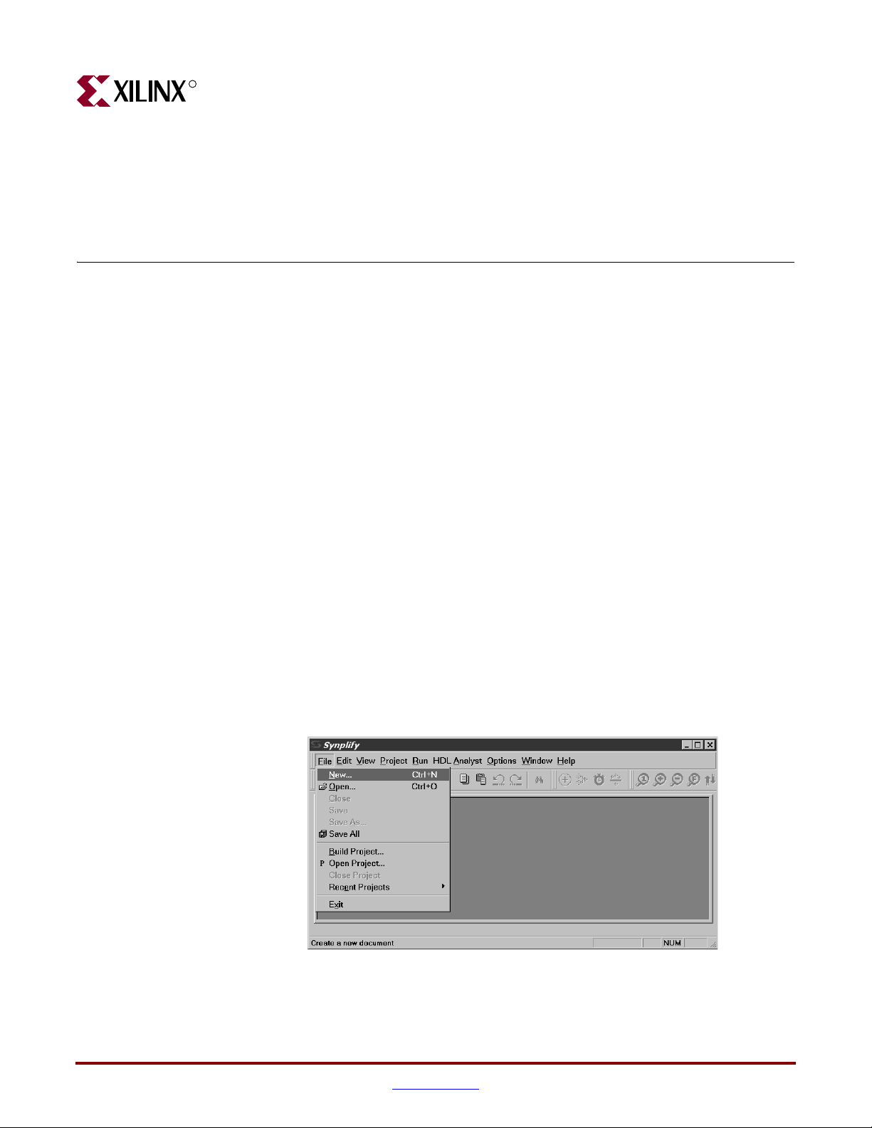
1. Start Synplify and choose File > New (Figure 5-1), or click the new file icon on the tool
bar.
The New dialog appears.
Figure 5-1: Create a New Project
PCI-X v5.1 165 Getting Started Guide www.xilinx.com 31
UG158 March 24, 2008

Chapter 5: Synthesizing a Design
R
2. Under File Type, select Project File and enter the project name (flowtest in this example)
and synthesis directory:
<Install Path>/verilog/example/synthesis
3. Click OK to return to the project window (Figure 5-2).
Figure 5-2: Main Project Window
4. To add source files to the new project, click Add. The first file (used by any design that
instantiates Xilinx primitives) is located in:
<Synplicity Install Path>/lib/xilinx
32 www.xilinx.com PCI-X v5.1 165 Getting Started Guide
UG158 March 24, 2008

Synplicity Synplify
R
5. Navigate to the virtex.v file (Figure 5-3); then click Add to move this source file into the
Files To Add list.
Figure 5-3: Files to Add (Virtex Library)
The next files are located in:
<Install Path>/verilog/src/xpci
6. Navigate to the xpci directory (Figure 5-4), select the simulation model and the
wrapper files (pcix_core.v and pcix_lc.v), and click Add to move these files into the
Files To Add list. (Ctrl + click to select multiple files.)
Figure 5-4: Files to Add (LogiCORE Files)
The final set of design files (the user application) is located in:
<Install Path>/verilog/example/source
PCI-X v5.1 165 Getting Started Guide www.xilinx.com 33
UG158 March 24, 2008

Chapter 5: Synthesizing a Design
R
7. Navigate to the source directory (Figure 5-5), select the cfg_test_s.v, pcix_top.v, and
userapp.v files, and then click Add.
Figure 5-5: Files to Add (User Application)
8. After adding the three final files (for a total of six source files), click OK to return to the
main project window.
9. In the Source Files list, view the list of newly added source files by double-clicking the
flowtest/verilog folder (if it is not already open). Reorder the source files in the
folder by dragging them to list them in the hierarchical order displayed in Figure 5-6.
Figure 5-6: Source Files in Main Project Window
34 www.xilinx.com PCI-X v5.1 165 Getting Started Guide
UG158 March 24, 2008

Synplicity Synplify
R
10. Click Change Result File to display the EDIF Result File dialog box; then move the to
following directory:
<Install Path>/verilog/example/synthesis
11. Name the file pcix_top_s.edf and click OK to set the name of the result file and
return to the main project window.
Note:
the sample processing scripts included with the example design assume that the output EDIF
files will be located in the synthesis directory.
In practice, the directory for the EDIF result file does not need to be changed. However,
12. From the main project window, click Change Target to display the Options for
Implementation dialog, Figure 5-7.
Figure 5-7: Options for Implementation: Device
13. On the Device tab, set the Technology, Part, Speed, and Package options to reflect the
targeted device (a 2V1000FG456-5 in this example). Be sure that Disable I/O Insertion
is deselected.
14. On the Options/Constraints tab, deselect Symbolic FSM Compiler (but leave Resource
Sharing selected) and set the Frequency to 66 MHz.
Figure 5-8: Options for Implementation: Options/Constraints
PCI-X v5.1 165 Getting Started Guide www.xilinx.com 35
UG158 March 24, 2008

R
VHDL
Chapter 5: Synthesizing a Design
15. On the Implementation Results tab, deselect Write Vendor Constraint File.
16. Click OK to return to the main project window.
17. From the main project window, click Run.
Synplify synthesizes the design and writes out an optimized EDIF file. In the lowerright corner of the window, the various stages or synthesis, such as Compiling or
Mapping, are displayed.
When the process is complete, Done is displayed. Synplify may issue a number of
warnings (which are expected) about instantiated I/O cells and attributes used for
other synthesis tools.
1. Start Synplify and choose File > New (Figure 5-9), or use the new file icon on the tool
bar. The New dialog appears.
Figure 5-9: Create a New Project
2. Under File Type, select Project File and enter the project name (flowtest in this example)
and synthesis directory:
<Install Path>/vhdl/example/synthesis
36 www.xilinx.com PCI-X v5.1 165 Getting Started Guide
UG158 March 24, 2008

Synplicity Synplify
R
3. Click OK to exit the dialog and return to the project window (Figure 5-10).
Figure 5-10: Main Project Window
4. To add source files to the new project, click Add.
The first file (used by any design that instantiates Xilinx primitives) is located in:
<Synplicity Install Path>/lib/xilinx
5. Select the virtex.vhd file (Figure 5-11); then click Add to move the file into the Files
To Add l i st.
Figure 5-11: Files to Add (Virtex Library)
PCI-X v5.1 165 Getting Started Guide www.xilinx.com 37
UG158 March 24, 2008

Chapter 5: Synthesizing a Design
R
The next files are located in:
<Install Path>/vhdl/src/xpci
6. Navigate to the xpci directory (Figure 5-12), select the simulation model and the
wrapper files (pcix_core.vhd and pcix_lc.vhd), and click Add to move these files into
the Files To Add list. (Ctrl + click to select multiple files.)
Figure 5-12: Files to Add (LogiCORE Files)
The final set of design files (the user application) is located in:
<Install Path>/vhdl/example/source
7. Navigate to the source directory (Figure 5-13), select the cfg_test_s.vhd, pcix_top.vhd,
and userapp.vhd, then click Add.
Figure 5-13: Files to Add (User Application)
38 www.xilinx.com PCI-X v5.1 165 Getting Started Guide
UG158 March 24, 2008

Synplicity Synplify
R
8. In the Source Files list, view the list of newly added source files by double-clicking the
flowtest/vhdl folder (if it is not already open). Drag to reorder the source files in
the hierarchical order shown in Figure 5-14.
Figure 5-14: Main Project Window
9. Click Change Result File to display the EDIF Result File dialog box; then move the to
following directory:
<Install Path>/vhdl/example/synthesis
10. Name the file pcix_top.edf and click OK to set the name of the result file and return
to the main project window.
Note:
the sample processing scripts included with the example design assume that the output EDIF
files will be located in the synthesis directory.
In practice, the directory for the EDIF result file does not need to be changed. However,
PCI-X v5.1 165 Getting Started Guide www.xilinx.com 39
UG158 March 24, 2008

Chapter 5: Synthesizing a Design
R
11. From the main project window, click Change Target to display the Options for
Implementation dialog box, as shown in Figure 5-15.
Figure 5-15: Options for Implementation: Device
12. On the Device tab, set the Technology, Part, Speed, and Package options to reflect the
targeted device (a 2V1000FG456-5 in this example). Be sure that Disable I/O Insertion
is deselected.
13. On the Options/Constraints tab, deselect Symbolic FSM Compiler (leave Resource
Sharing selected) and set the Frequency to 66 MHz.
14. On the Implementation Results tab, deselect Write Vendor Constraint File.
15. Click OK to return to the main project window; then click Run.
Synplify synthesizes the design and writes out an optimized EDIF file. In the lowerright corner of the window, the various stages or synthesis, such as Compiling or
Mapping, are displayed. When the process is complete, Done is displayed. Note that
Synplify may issue a number of warnings (which are expected) about instantiated I/O
cells and attributes used for other synthesis tools.
Exemplar LeonardoSpectrum
Before attempting to synthesize a design, ensure that the Exemplar LeonardoSpectrum
environment is properly configured for use.
1. Navigate to the synthesis directory:
cd <Install Path>/hdl/example/synthesis
The synthesis directory contains a script for use with LeonardoSpectrum.
2. Edit the script to change the following line:
cd <Install Path>/hdl/example/synthesis
Modify the path to point to the actual installation location, and then save the file.
3. Invoke LeonardoSpectrum.
Depending on the implementation, you may also need to change the wrapper file and
the simulation model, but this is not required for the example design.
4. Synthesize the design by running the leonardo_s.tcl script.
40 www.xilinx.com PCI-X v5.1 165 Getting Started Guide
UG158 March 24, 2008

Xilinx XST
R
Note: if you run LeonardoSpectrum with the graphical user interface, the quick setup form cannot be
used to synthesize the design. Instead, choose File > Run Script from the menu.
The end result of the synthesis step is an EDIF file that is fed into the Xilinx implementation
tools during the implementation step.
In practice, the provided script file must be modified to accommodate other designs. To
provide insight into the synthesis script, the major steps are presented below:
1. Various synthesis options are set through the use of environment variables. These
must be present in the script, and should not be modified. The synthesis library is also
loaded; this may be altered for different devices and speed grades.
2. The design is loaded by reading in the design files. At this point, the top level module
is declared as the present_design. The script adds nopad attributes (with a value of
FALSE) to all PCI-X bus interface signals. The I/O structures for these ports are
directly instantiated in the wrapper file.
3. The optimization step is done with the -hierarchy preserve and the -chip
options. The -hierarchy preserve option prevents LeonardoSpectrum from
dissolving the design hierarchy. The -chip option indicates that automatic I/O buffer
insertion should be performed.
4. After synthesis is complete, the synthesized netlist is written out.
5. The tool may issue warnings about unused signals. These warnings are expected.
Xilinx XST
Before attempting to synthesize a design, ensure that the Xilinx XST environment is
properly configured. Synthesis is supported only from the XST command line.
1. Navigate to the synthesis directory:
cd <Install Path>/hdl/example/synthesis
The synthesis directory contains a script for use with Xilinx XST; this script is called
run_xst.bat for PC platforms and run_xst.sh for Unix platforms. Note that the
run_xst.cmd and run_xst.prj files are common and used by both scripts.
2. If required, modify the files as required to suit your application. You may need to
change the target architecture and select different wrapper and configuration files.
3. Synthesize the design by running the script.
The end result of the synthesis step is an NGC file, which is fed into the Xilinx
implementation tools during the implementation step. The tool may issue warnings about
unused signals; these warnings are expected.
PCI-X v5.1 165 Getting Started Guide www.xilinx.com 41
UG158 March 24, 2008

Chapter 5: Synthesizing a Design
R
42 www.xilinx.com PCI-X v5.1 165 Getting Started Guide
UG158 March 24, 2008

R
Implementing a Design
This chapter describes the use of supported FPGA implementation tools using the Userapp
example design. If you are using a design with reference clocks, substitute pcix_top with
pcix_top_r and test_tb with test_tb_r.
Supported FPGA implementation tools are included with the ISE Foundation v10.1
software.
ISE Foundation
Before implementing a design, ensure that the Xilinx environment is properly configured
and that the design has been successfully synthesized.
1. Navigate to the implementation directory:
cd <Install Path>/hdl/example/xilinx
This directory contains the run_xil_n, run_xil_s, and run_xil_x scripts. These
call the appropriate tools to place and route the example design in one of three possible
incarnations: PCI only, Dual Mode, and PCI-X only. Use the script that corresponds to
the core configuration you have selected. For the default example design, the Dual
Mode script should be used.
Chapter 6
2. Inspect the appropriate script file and note the following:
♦ The ngdbuild command lists both../../src/xpci and../synthesis as
search directories. The xpci directory contains a netlist of the core interface, and
the synthesis directory must contain the EDIF netlist generated during design
synthesis.
♦ The ngdbuild command also reads a user constraints file that corresponds to a
desired target device and a particular version of the core interface.
♦ To target a different device or to use a different version of the core interface, the
constraints file must be changed to match the device and interface selection. The
available selections are listed in the Chapter 3, “Family Specific Considerations.”
♦ The user constraints files provided with the core interface contain constraints that
guarantee pinout and timing specifications. These constraints must be used
during processing.
♦ Any additional constraints that pertain to the user application must be placed in
this file. Before making additions to the user constraints file, back up the original
so that it may be restored if necessary.
♦ The map command requires no special arguments, but uses an input/output
register packing option.
♦ The PAR effort levels and delay cleanup iterations may be adjusted if necessary.
PCI-X v5.1 165 Getting Started Guide www.xilinx.com 43
UG158 March 24, 2008

Chapter 6: Implementing a Design
R
♦ The trce command performs a static timing analysis based on the design
constraints originally specified in the user constraints file.
♦ The netgen command generates a simulation model of the placed and routed
design.
3. Implement the design by running the appropriate script.
During initial processing trials, it is useful to enter the commands one at a time from the
command line, instead of running the script, so that you may inspect the output of each
step.
44 www.xilinx.com PCI-X v5.1 165 Getting Started Guide
UG158 March 24, 2008

R
Timing Simulation
This chapter describes the use of supported timing simulation tools using the Userapp
example design. If you are using a design with reference clocks, substitute pcix_top with
pcix_top_r and test_tb with test_tb_r.
Supported timing simulation tools include
• Cadence IUS v6.1
• Mentor Graphics ModelSim v6.3c
Note: The stimulus source file delivered with the example design
(source/stimulus.hdl) simulates in both PCI and PCI-X mode, automatically
detecting the proper mode and bus speed based on power-on signaling.
Cadence IUS
Chapter 7
Before attempting timing simulation, ensure that the IUS environment is properly
configured for use.
1. Navigate to the timing simulation directory and copy the back annotated timing
models from the implementation directory:
cd <Install Path>/verilog/example/post_sim
cp ../xilinx/*.v ./
cp ../xilinx/*.sdf ./
2. Edit the test_tb.f file. This file lists command line arguments for IUS, and is shown
below:
../source/stimulus.v
../source/test_tb.v
../source/busrec.v
./pcix_top_s_routed.v
+libext+.vmd+.v
-y <Xilinx Install Path>/verilog/src/simprims
Modify the library search path by changing <Xilinx Install Path> to match the
Xilinx installation directory. Save the file.
3. To run the IUS simulation, type the following:
ncverilog -f test_tb.f
IUS processes the simulation files and exits. The test bench prints status messages to the
console. After the simulation completes, view the ncverilog.log file to check for errors.
PCI-X v5.1 165 Getting Started Guide www.xilinx.com 45
UG158 March 24, 2008

R
The SimVision browser may be used to view simulation results. SimVision is started with
the following command:
simvision
Mentor Graphics ModelSim
Before attempting functional simulation, ensure that the ModelSim environment is
properly configured for use.
Verilog
1. Navigate to the timing simulation directory and copy the back annotated timing
models from the implementation directory:
cd <Install Path>/verilog/example/post_sim
cp ../xilinx/*.v ./
cp ../xilinx/*.sdf ./
2. Edit the test_tb.f file. This file lists command line arguments for ModelSim, and is
shown below:
../source/stimulus.v
../source/test_tb.v
../source/busrec.v
./pcix_top_s_routed.v
+libext+.vmd+.v
-y <Xilinx Install Path>/verilog/src/simprims
Modify the library search path by changing <Xilinx Install Path> to match the
Xilinx installation directory. Save the file.
Chapter 7: Timing Simulation
VHDL
3. Invoke ModelSim, and ensure that the current directory is set to:
<Install Path>/verilog/example/post_sim
4. To run the simulation:
do modelsim.do
This compiles all modules, loads them into the simulator, displays the waveform viewer,
and runs the simulation.
1. Navigate to the timing simulation directory and copy the back annotated timing
models from the implementation directory:
cd <Install Path>/vhdl/example/post_sim
cp ../xilinx/*.vhd ./
cp ../xilinx/*.sdf ./
2. View the test.files file. This file lists the individual source files required, and is
shown below:
./pcix_top_s_routed.vhd
../source/busrec.vhd
../source/stimulus.vhd
../source/test_tb.vhd
46 www.xilinx.com PCI-X v5.1 165 Getting Started Guide
UG158 March 24, 2008

Mentor Graphics ModelSim
R
3. Invoke ModelSim, and ensure that the current directory is set to:
4. Create the SimPrim and UniSim libraries. This step only needs to be done once, the
5. To run the simulation:
<Install Path>/vhdl/example/post_sim
first time you perform a simulation:
vlib simprim
vcom -93 -work simprim <Xilinx Install
Path>/vhdl/src/simprims/simprim_Vpackage_mti.vhd
vcom -93 -work simprim <Xilinx Install
Path>/vhdl/src/simprims/simprim_Vcomponents_mti.vhd
vcom -93 -work simprim <Xilinx Install
Path>/vhdl/src/simprims/simprim_VITAL_mti.vhd
vlib unisim
vcom -93 -work unisim <Xilinx Install
Path>/vhdl/src/unisims/unisim_VPKG.vhd
vcom -93 -work unisim <Xilinx Install
Path>/vhdl/src/unisims/unisim_VCOMP.vhd
vcom -93 -work unisim <Xilinx Install
Path>/vhdl/src/unisims/unisim_VITAL.vhd
do modelsim.do
This compiles all modules, loads them into the simulator, displays the waveform
viewer, and runs the simulation.
PCI-X v5.1 165 Getting Started Guide www.xilinx.com 47
UG158 March 24, 2008
 Loading...