

Page 1
co.com
0
PCI32 Interface v3.0
DS206 August 31, 2005
00
Features
• Fully PCI 3.0-compliant LogiCORE™, 32-bit, 66/33
MHz interface
• Customizable, programmable, single-chip solution
• Pre-defined implementation for predictable timing
• Incorporates Xilinx Smart-IP™ technology
• 3.3V operation at 0-66 MHz
• 5.0V operation at 0-33 MHz
• Fully verified design tested with Xilinx proprietary
testbench and hardware
• Available through the Xilinx CORE Generator™
v7.1i or higher
• CardBus compliant
• Supported initiator functions:
- Configuration read, configuration write
- Memory read, memory write, MRM, MRL
- Interrupt acknowledge, special cycles
- I/O read, I/O write
• Supported target functions:
- Type 0 configuration space header
- Up to three base address registers (MEM or I/O
with adjustable block size from 16 bytes to 2 GB)
- Medium decode speed
- Parity generation, parity error detection
- Configuration read, configuration write
- Memory read, memory write, MRM, MRL
Product Specification v3.0.151
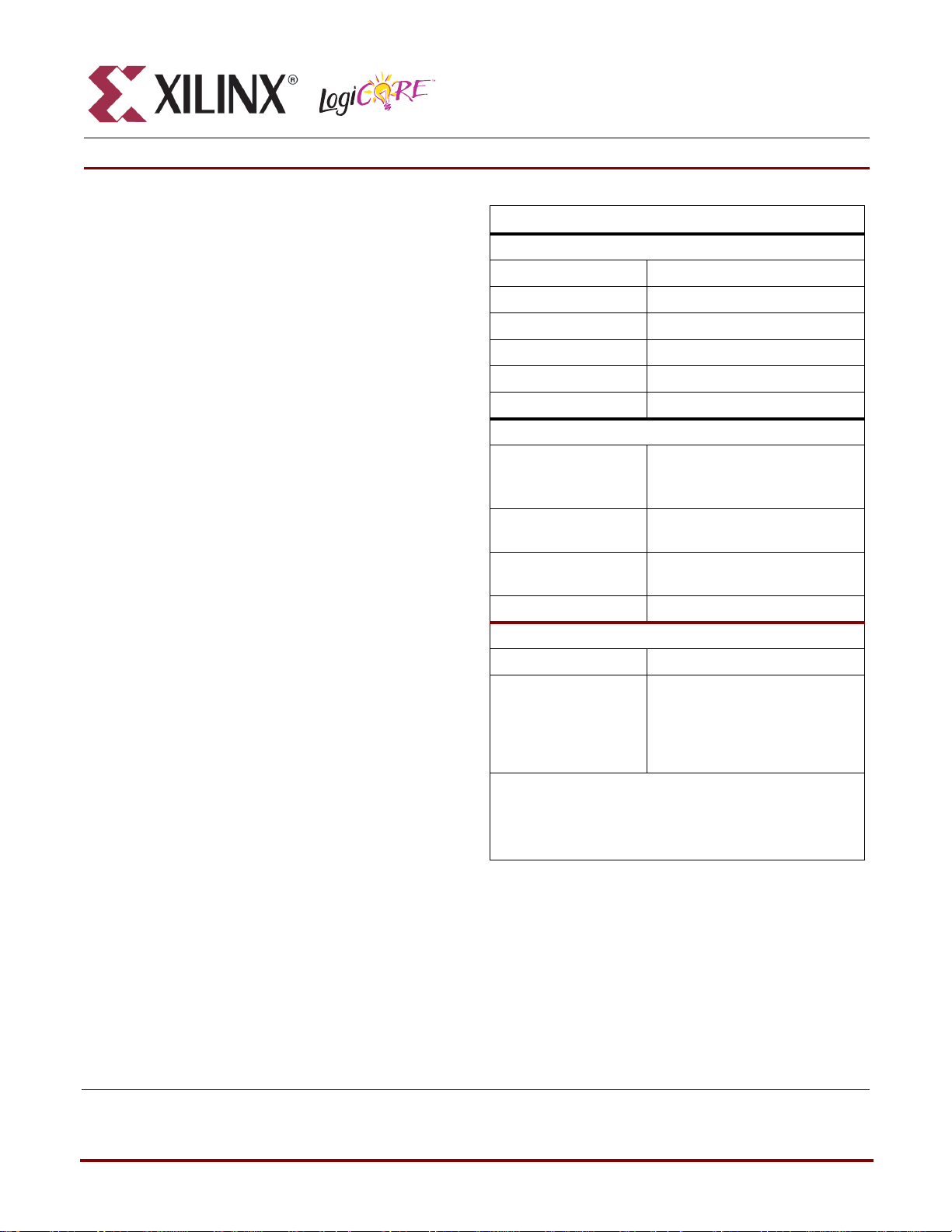
LogiCORE Facts
PCI32 Resource Utilization
Slice Four Input LUTs 553
Slice Flip-Flops 566
IOB Flip-Flops 97
IOBs 50
TBUFs 288
GCLKs 1
Provided with Core
PCI32 Product Specification
Documentation
Design File Formats
Constraints Files
PCI Getting Started Guide
Verilog/VHDL Simulation Model
User Constraints File (UCF)
Example Design Verilog/VHDL Example Design
Design Tool Requirements
Xilinx Tools v7.1i Service Pack 4
Tested Entry and
Verification Tools
Xilinx provides technical support for this LogiCORE product when
used as described in the PCI Getting Started Guide and PCI User
Guide. Xilinx cannot guarantee timing, functionality, or support of
product if implemented in devices not listed, or if customized
beyond that allowed in the product documentation.
(3)
Model Technology ModelSim
Exemplar LeonardoSpectrum
(1)
(2)
PCI User Guide
NGO Netlist
Guide File (NCD)
Synplicity Synplify
Xilinx XST
(4)
Cadence NC-Verilog
- Interrupt acknowledge
- I/O read, I/O write
- Target abort, target retry, target disconnect
© 2005 Xilinx, Inc. All rights reserved. XILINX, the Xilinx logo, and other designated brands included herein are trademarks of Xilinx, Inc. All other trademarks are the property of their respective
owners. Xilinx is providing this design, code, or information "as is." By providing the design, code, or information as one possible implementation of this feature, application, or standard, Xilinx
makes no representation that this implementation is free from any claims of infringement. You are responsible for obtaining any rights you may require for your implementation. Xilinx expressly
disclaims any warranty whatsoever with respect to the adequacy of the implementation, including but not limited to any warranties or representations that this implementation is free from
claims of infringement and any implied warranties of merchantability or fitness for a particular purpose.
DS206 August 31, 2005 www.xilinx.com 1
Product Specification v3.0.151
Page 2
PCI32 Interface v3.0
Fact Table Notes
1. Resource utilization depends on configuration of the interface and user design. Unused resources are trimmed by the Xilinx
technology mapper. The utilization figures reported in this table are representative of a maximum configuration.
2. Designs running at 66 MHz in devices other than Virtex-II, Virtex-II Pro, Virtex-4, Spartan-3, and Spartan-3E require one
GCLKIOB and two GCLKs. Virtex-4 implementations require additional BUFG for 200 MHz reference clock.
3. See the PCI Getting Started Guide or product release notes for current supported versions.
4. XST is a command line option only. See the PCI Getting Started Guide for details.
5. Universal card implementations require two bitstreams.
6. Virtex and Spartan-II not recommended for CardBus.
7. Commercial devices: 0
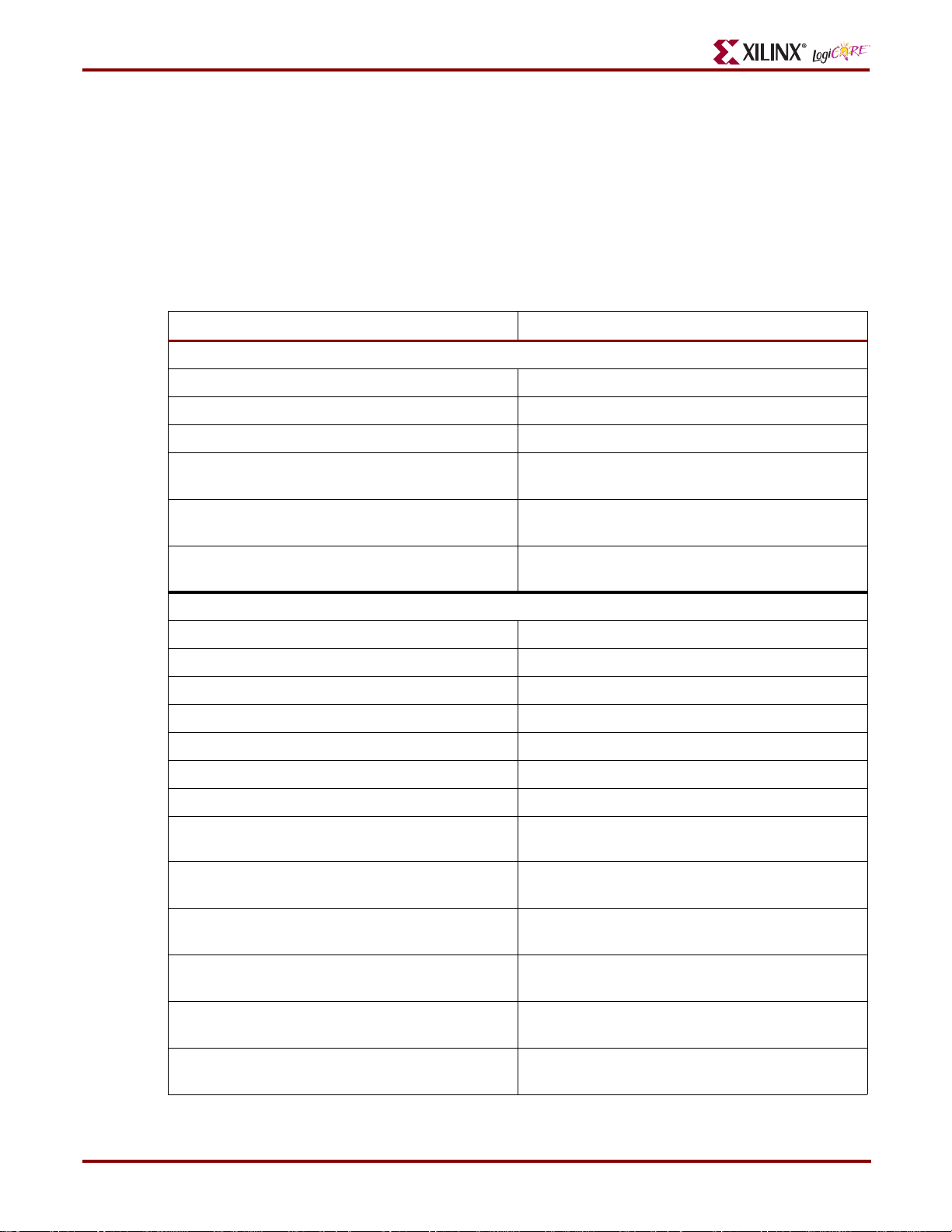
Table 1: Core Implementation
Virtex™ XCV200-FG256-6C 3.3V only
Virtex-E XCV200E-FG256-6C 3.3V only
Virtex-E XCV400E-FG676-6C 3.3V only
Virtex-4 XC4VLX25-FF668-11C/I
(regional clock based)
Virtex-4 XC4VSX35-FF668-11C/I
(regional clock based)
Virtex-4 XC4VFX20-FF672-11C/I
(regional clock based)
o
C < Tj < 85oC.
Supported Device Power Supply
PCI32/66
(6,7)
(6,7)
(6,7)
3.3V only
3.3V only
3.3V only
PCI32/33
Virtex XCV300-BG432-5C 3.3V, 5.0V only
Virtex XCV1000-FG680-5C 3.3V, 5.0V only
Virtex-E XCV100E-BG352-6C 3.3V only
Virtex-E XCV300E-BG432-6C 3.3V only
Virtex-E XCV1000E-FG680-6C 3.3V only
Virtex-II XC2V1000-FG456-4C/I/M 3.3V only
Virtex-II Pro XC2VP7-FF672-5C/I 3.3V only
Virtex-4 XC4VLX25-FF668-10C/I
(regional clock based)
Virtex-4 4 XC4VSX35-FF668-10C/I
(regional clock based)
Virtex-4 XC4VFX20-FF672-10C/I
(regional clock based)
Virtex-4 XC4VLX25-FF668-10C/I
(global clock based)
Virtex-4 XC4VSX20-FF668-10C/I
(global clock based)
Virtex-4 XC4VFX20-FF672-10C/I
(global clock based)
(6,7)
3.3V only
(6,7)
3.3V only
(6,7)
3.3V only
(6,7)
3.3V only
(6,7)
3.3V only
(6,7)
3.3V only
2 www.xilinx.com DS206 August 31, 2005
Product Specification v3.0.151
Page 3
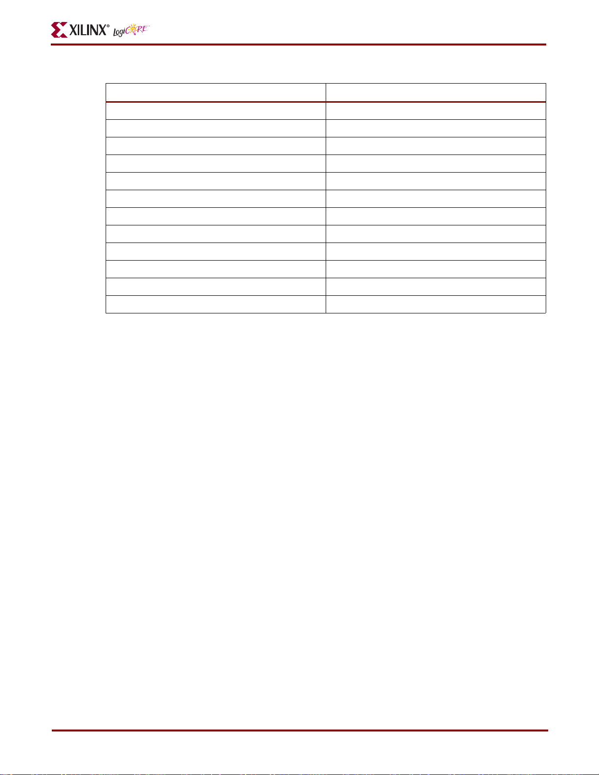
Table 1: Core Implementation (Continued)
Supported Device Power Supply
Spartan™-II XC2S30-PQ208-5C 3.3V, 5.0V only
PCI32 Interface v3.0
Spartan-II XC2S50-PQ208-5C
Spartan-II XC2S100-PQ208-5C
Spartan-II XC2S150-PQ208-5C
Spartan-II XC2S200-PQ208-5C
Spartan-IIE 2S50E-PQ208-6C
Spartan-IIE XC2S100E-PQ208-6C
Spartan-IIE XC2S150E-PQ208-6C
Spartan-IIE XC2S200E-PQ208-6C
Spartan-IIE XC2S300E-PQ208-6C
Spartan-3 XC3S1000-FG456-4C/I
Spartan-3E XC3S1200E-FG400-4C/I
(1)
3.3V, 5.0V only
3.3V, 5.0V only
3.3V, 5.0V only
3.3V, 5.0V only
3.3V only
3.3V only
3.3V only
3.3V only
3.3V only
3.3V only
3.3V only
Notes
1. Spartan-3 and Spartan-3E solution pending production speed files.
2. For additional Part/Package combinations, see the UCF Generator in the PCI Lounge.
3. XC2V1000 is supported over Military Temp. range
4. Spartan-3, Spartan-3E, and Virtex-4 devices do not contain TBUFs. The Xilinx tools automatically translate TBUFs to LUTs,
and they are included in the worst case LUT count listed.
5. Virtex-II Pro, Virtex-4, Spartan-3, and Spartan-3E devices are supported over commercial and industrial temperature ranges.
6. As shipped, the core is verified for timing compliance with speedfile versions 1.56 and later. This applies to all production
devices and most engineering samples. If you are using engineering samples that require the 1.54 speedfile, please contact
Xilinx Customer Applications..
7. Requires 200 MHz reference clock.
Applications
• Embedded applications in networking, industrial, and telecommunication systems
• PCI add-in boards such as frame buffers, network adapters, and data acquisition boards
• Hot swap CompactPCI boards
• CardBus compliant
• Any applications that need a PCI interface
General Description
The Xilinx PCI interface is a pre-implemented and fully tested module for Xilinx FPGAs. The pinout for
each device and the relative placement of the internal logic are predefined. Critical paths are controlled
by constraints and guide files to ensure predictable timing. This significantly reduces engineering time
required to implement the PCI portion of your design. Resources can instead be focused on your
unique user application logic in the FPGA and on the system-level design. As a result, Xilinx PCI products minimize your product development time.
The core meets the setup, hold, and clock-to-timing requirements as defined in the PCI specification.
The interface is verified through extensive simulation.
DS206 August 31, 2005 www.xilinx.com 3
Product Specification v3.0.151
Page 4

PCI32 Interface v3.0
Other FPGA resources that can be used in conjunction with the core to enable efficient implementation
of a PCI system include:
• Block SelectRAM™ memory. Blocks of on-chip ultra-fast RAM with synchronous write and
dual-port RAM capabilities. Used in PCI designs to implement FIFOs.
• SelectRAM memory. Distributed on-chip ultra-fast RAM with synchronous write option and
dual-port RAM capabilities. Used in PCI designs to implement FIFOs.
• Internal three-state bus capability for data multiplexing.
The interface is carefully optimized for best possible performance and utilization in Xilinx FPGA
devices.
Smart-IP Technology
Drawing on the architectural advantages of Xilinx FPGAs, Xilinx Smart-IP technology ensures the
highest performance, predictability, repeatability, and flexibility in PCI designs. The Smart-IP technology is incorporated in every PCI interface.
Xilinx Smart-IP technology leverages the Xilinx architectural advantages, such as look-up tables and
segmented routing, as well as floorplanning information, such as logic mapping and location constraints. This technology provides the best physical layout, predictability, and performance. In addition, these features allow for significantly reduced compile times over competing architectures.
To guarantee the critical setup, hold, minimum clock-to-out, and maximum clock-to-out timing, the
PCI interface is delivered with Smart-IP constraint files that are unique for a device and package combination. These constraint files guide the implementation tools so that the critical paths always are
within specification.
Xilinx provides Smart-IP constraint files for many device and package combinations. Constraint files
for unsupported device and package combinations may be generated using the web-based constraint
file generator.
Functional Description
4 www.xilinx.com DS206 August 31, 2005
Product Specification v3.0.151
Page 5

PCI32 Interface v3.0
Figure 1 illustrates a user application and the PCI Interface partitioned into five major blocks.
Figure Top x-ref 1
PA R
PAR64
PERR-
SERR-
Parity
Generator/
Checker
Base
Address
Register
0
Base
Address
Register
1
Base
Address
Register
2
Command/
Status
Register
PCI I/O INTERFACE
AD[63:0]
FRAME-
IRDY-
REQ-
GNT-
REQ64-
ACK64-
TRDY-
DEVSEL-
STOP-
Initiator
State
Machine
Target
State
Machine
ADIO[63:0]
ADIO[63:0]
Interrupt
Pin and
Line
Register
PCI Configuration Space
Latency
Timer
Register
Vendor ID,
Rev ID,
Other User
Data
USER APPLICATION
Figure 1: PCI Interface Block Diagram
PCI I/O Interface Block
The I/O interface block handles the physical connection to the PCI bus including all signaling, input
and output synchronization, output three-state controls, and all request-grant handshaking for bus
mastering.
User Application
The PCI Interface provides a simple, general-purpose interface for a wide range of applications.
PCI Configuration Space
This block provides the first 64 bytes of Type 0, version 3.0 Configuration Space Header, as shown in
Tab le 2, to support software-driven Plug-and-Play initialization and configuration. This includes infor-
mation for Command and Status, and three Base Address Registers (BARs).
The capability for extending configuration space has been built into the user application interface. This
capability, including the ability to implement a capabilities pointer in configuration space, allows the
user to implement functions such as power management and message signaled interrupts in the user
application.
Parity Generator/Checker
This block generates and checks even parity across the AD bus, the CBE# lines, and the parity signals.
It also reports data parity errors via PERR# and address parity errors via SERR#.
Initiator State Machine
This block controls the PCI interface initiator functions. The states implemented are a subset of those
defined in Appendix B of the PCI Local Bus Specification. The initiator control logic uses one-hot encod-
ing for maximum performance.
DS206 August 31, 2005 www.xilinx.com 5
Product Specification v3.0.151
Page 6

PCI32 Interface v3.0
Target State Machine
This block controls the PCI interface target functions. The states implemented are a subset of those
defined in Appendix B of the PCI Local Bus Specification. The target control logic uses one-hot encoding
for maximum performance.
Table 2: PCI Configuration Space Header
31 16 15 0
BIST Header
Max Lat Min Gnt Int Pin Int Line
Note: Shaded areas are not implemented and return zero.
Device ID Vendor ID
Status Command
Class Code Rev ID
Type
Base Address Register 0 (BAR0)
Base Address Register 1 (BAR1)
Base Address Register 2 (BAR2)
Base Address Register 3 (BAR3)
Base Address Register 4 (BAR4)
Base Address Register 5 (BAR5)
Cardbus CIS Pointer
Subsystem ID Subsystem Vendor ID
Expansion ROM Base Address
Reserved CapPtr
Latency
Timer
Reserved
Reserved
Cache Line
Size
00h
04h
08h
0Ch
10h
14h
18h
1Ch
20h
24h
28h
2Ch
30h
34h
38h
3Ch
40h-FFh
Interface Configuration
The PCI Interface can be easily configured to fit unique system requirements using the Xilinx CORE
Generator GUI or by changing the HDL configuration file. The following customization options,
among many others, are supported by the interface and are described in the PCI User Guide.
• Device and vendor ID
• Base Address Registers (number, size, and type)
Burst Transfer
The PCI bus derives its performance from its ability to support burst transfers. The performance of any
PCI application depends largely on the size of the burst transfer. Buffers to support PCI burst transfer
can efficiently be implemented using on-chip RAM resources.
Supported PCI Commands
Tab le 3 illustrates the PCI bus commands supported by the PCI Interface.
6 www.xilinx.com DS206 August 31, 2005
Product Specification v3.0.151
Page 7

PCI32 Interface v3.0
Bandwidth
The PCI Interface supports fully compliant zero wait-state burst operations for both sourcing and
receiving data. This interface supports a sustained bandwidth of up to 264 MBytes/sec. The design can
be configured to take advantage of the ability of the PCI Interface to do very long bursts.
The flexible user application interface, combined with support for many different PCI features, gives
users a solution that lends itself to use in many high-performance applications. The user is not locked
into one DMA engine; hence, an optimized design that fits a specific application can be designed.
Recommended Design Experience
The PCI Interface is pre-implemented, allowing engineering focus on the unique user application functions of a PCI design. Regardless, PCI is a high-performance design that is challenging to implement in
any technology. Therefore, previous experience with building high-performance, pipelined FPGA
designs using Xilinx implementation software, constraint files, and guide files is recommended. The
challenge to implement a complete PCI design including user application functions varies depending
on configuration and functionality of your application. Contact your local Xilinx representative for a
closer review and estimation for your specific requirements.
DS206 August 31, 2005 www.xilinx.com 7
Product Specification v3.0.151
Page 8

PCI32 Interface v3.0
Timing Specifications
The maximum speed at which your user design is capable of running can be affected by the size and
quality of the design. The following tables show the key timing parameters for the PCI Interface.
Tab le 4 lists the Timing Parameters in the 66 MHz Implementations and Tab le 5 lists Timing Parameters
in the 33 MHz Implementations.
Table 3: PCI Bus Commands
CBE [3:0] Command
0000 Interrupt Acknowledge Yes Yes
0001 Special Cycle Yes Ignore
0010 I/O Read Yes Yes
0011 I/O Write Yes Yes
0100 Reserved Ignore Ignore
0101 Reserved Ignore Ignore
0110 Memory Read Yes Yes
0111 Memory Write Yes Yes
1000 Reserved Ignore Ignore
1001 Reserved Ignore Ignore
1010 Configuration Read Yes Yes
1011 Configuration Write Yes Yes
1100 Memory Read Multiple Yes Yes
1101 Dual Address Cycle No Ignore
1110 Memory Read Line Yes Yes
PCI
Initiator
PCI
Target
1111 Memory Write Invalidate No Yes
8 www.xilinx.com DS206 August 31, 2005
Product Specification v3.0.151
Page 9

PCI32 Interface v3.0
Table 4: Timing Parameters, 66 MHz Implementations
Symbol Parameter Min Max
T
T
T
T
cyc
high
low
val
CLK Cycle Time 15
CLK High Time 6 -
CLK Low Time 6 -
CLK to Signal Valid Delay
(bussed signals)
1
2
2
30
6
2
T
val
T
on
T
off
T
su
T
su
T
h
T
rstoff
Notes
1. Controlled by timespec constraints, included in product.
2. Controlled by SelectIO configured for PCI66_3.
3. Controlled by guide file, included in product.
CLK to Signal Valid Delay
(point to point signals)
Float to Active Delay 2
Active to Float Delay - 14
Input Setup Time to CLK
(bussed signals)
Input Setup Time to CLK
(point to point signals)
Input Hold Time from CLK 0
Reset Active to Output Float - 40
2
2
2
2,3
3
2,3
5
2,3
Table 5: Timing Parameters, 33 MHz Implementations
Symbol Parameter Min Max
1
T
T
T
T
cyc
high
low
val
CLK Cycle Time
CLK High Time 11 -
CLK Low Time 11 -
CLK to Signal Valid Delay
(bussed signals)
30
2
2
2
6
-
1
-
-
-
-
2
11
T
val
T
on
T
off
T
su
T
su
T
h
T
rstoff
Notes
1. Controlled by timespec constraints, included in product.
2. Controlled by SelectIO configured for PCI33_3 or PCI33_5.
CLK to Signal Valid Delay
(point to point signals)
Float to Active Delay 2
Active to Float Delay - 28
Input Setup Time to CLK
(bussed signals)
Input Setup Time to CLK
(point to point signals)
Input Hold Time from CLK 0
Reset Active to Output Float - 40
10
2
2
2
2
7
2
2
11
2
-
1
-
-
-
DS206 August 31, 2005 www.xilinx.com 9
Product Specification v3.0.151
Page 10

PCI32 Interface v3.0
Ordering Information
Build v3.0.150 of the PCI core, with support added for Spartan-3E, is for available for download from the
Xilinx IP Center and can also be accessed through the Xilinx CORE Generator system v7.1i or higher.
The Xilinx CORE Generator is bundled with the ISE Foundation v7.1i software at no additional charge.
To purchase the Xilinx PCI core, please contact your local Xilinx sales representative.
Part Numbers
• DO-DI-PCI32-IP
- Access to the v3.0 PCI32 33 MHz Spartan and 66 MHz Virtex Families
• DX-DI-PCI32-SL
- Upgrade from PCI32 33 MHz Spartan only to v3.0 PCI32 33 MHz Spartan and 66 MHz Virtex
• DO-DI-PCI32-SP
- Access to the v3.0 PCI32 Spartan family project license
families
10 www.xilinx.com DS206 August 31, 2005
Product Specification v3.0.151
Page 11

Revision History
The following table shows the revision history for this document.
Date Version Revision
07/30/02 1.2 Style updates
12/18/02 1.3 Updated to build v3.0.103; v5.Ii, 1st feature: 32-bit was 64/32-bit
3/7/03 1.4 Updated to build v3.0.105; v5.2i
PCI32 Interface v3.0
4/14/03 1.5
5/8/03 1.6 Updated Xilinx tools to 5.2i SP2; added Note 10.
9/17/03 1.7
10/28/03 1.8
1/30/04 1.9 Updated to build v3.0.122, updated copyright information to 2004.
4/9/04 1.10
4/26/04 1.11
7/15/04 1.12
11/11/04 1.13
12/8/04 1.14 Updated to build 3.0.140 and Virtex-4 support.
3/7/05 1.15 Updated to Xilinx tools 7.1i and build v3.0.145.
5/13/2005 2.0 Updated build to 3.0.150, added support for Spartan-3E, addition of SP2.
8/31/05 3.0 Updated build to 3.0.151, updated SP 2 to SP 4 for ISE 7.1i
Updated to build v3.0.106; in LogiCORE Facts table, updated PC32/33 product
listings to include Spartan-3 device support.
Updated to build v3.0.113; in LogiCORE Facts table, Xilinx Tools v6.1i SP1 was v5.2i
SP2; date was May 8, 2003.
Updated to build v3.0.116, in Supported Devices table, added XC prefix to device
names.
Updated to build v3.0.126; updated Xilinx tools to 6.2i SP1; in supported devices
table, added notes 11 and 12; added suffix /I to all Virtex-II Pro devices.
Updated to build v3.0.128, updated Xilinx tools to 6.2i SP2, changed date to April 26,
2004.
Updated to build v3.0.129 and to support Xilinx tools v6.2i SP3. The data sheet is
updated to the new template.
Updated support for Xilinx tools v6.3i SP2; updated PCI spec to v3.0; added
Exemplar LeonardoSpectrum and Cadence NC-Verilog entry and verification tools.
DS206 August 31, 2005 www.xilinx.com 11
Product Specification v3.0.151
 Loading...