


TLP411E
Table of contents
 Loading...
FIE NO. 336-9612
TECHNICAL TRAINING MANUAL
3 LCD DATA PROJECTOR
TLP411U
TLP411E
Dec., 1996

CONTENTS
SECTION I
MAIN POWER SUPPLY
CIRCUIT................................. 1-1
1. OUTLINE .........................................1-2
1-1. Block Diagram........................................... 1-2
2. DESCRIPTION ABOUT
CIRCUIT OPERATION..................1-2
2-1. Surge Absorber Circuit............................. 1-2
2-2. Noise Filter Circuit.................................... 1-3
2-3. Rush Current Protection Circuit ............. 1-3
2-4. Smoothing/Rectifying Circuit................... 1-3
2-5. Inverter Circuit (Flyback) ........................ 1-4
2-6. Primary Control Circuit ........................... 1-4
2-7. Secondary Rectification &
Smoothing Circuit ..................................... 1-5
2-8. +6V Detection Circuit ............................... 1-5
2-9. +6V, +S6V, +15.5V Overvoltage
Protection Circuit ...................................... 1-5
2-10. +6V, +S6V Over Current
Protection Circuit................................... 1-6
2-11. Output ON/OFF Circuit........................ 1-6
2-12. ON/OFF Control Circuit ....................... 1-6
2-3. Level Shifter Circuit
(Q965 – Q968, R1044) ............................... 4-4
2-4. Black Limiter (Q969, Q970)..................... 4-4
2-5. Inverted Signal Amplifiers
(Q974 – Q981) ............................................ 4-4
2-6. Switch Circuit
(Q982 µPD74HC4066A)........................... 4-4
2-7. Sample & Hold Circuit............................. 4-5
2-8. LCD Panel.................................................. 4-7
SECTION V
MICROCOMPUTER............. 5-1
1. SYSTEM OUTLINE ........................5-2
2. SYSTEM MICROCOMPUTER .....5-4
3. POWER SUPPLY RESET
PROCESS..........................................5-5
4. NON-VOLATILE MEMORY
PROCESS..........................................5-5
5. REMOTE CONTROL
RECEPTION PROCESS.................5-6
SECTION II
LAMP HIGH VOLTAGE
POWER SUPPLY
CIRCUIT................................. 2-1
1. LAMP HIGH VOLTAGE
POWER SUPPLY.............................2-2
SECTION III
OPTICAL SYSTEM .............. 3-1
1. CONFIGURATION ......................... 3-2
SECTION IV
RGB DRIVE CIRCUIT ......... 4-1
1. OUTLINE .........................................4-2
2. CIRCUIT DESCRIPTION ..............4-2
2-1. Level Shifter (Q945 – Q953)..................... 4-2
2-2. Gamma (
gg
g) Circuit ..................................... 4-3
gg
6. RS-232C TRANSMIT/
RECEIVE PROCESS ......................5-6
7. STATUS READ PROCESS .............5-7
8. STATUS DISPLAY PROCESS........5-7
9. ON-SCREEN DISPLAY
PROCESS..........................................5-8
10. VIDEO MODE FETCH
PROCESS.......................................5-8
11. VIDEO SYSTEM CONTROL
PROCESS.......................................5-9
12. PANEL SYSTEM CONTROL
PROCESS......................................5-10
13. VARIOUS DISPLAY
MODES .........................................5-11
14. APPLICABLE SIGNAL ..............5-12
15. RS-232C CONTROL
METHOD......................................5-13
16. RS-232C COMMAND LIST ....... 5-13
i

SECTION VI
DIGITAL CIRCUIT............... 6-1
SECTION VIII
CCD CAMERA CIRCUIT .... 8-1
1. DIGITAL CIRCUIT
OPERATION ....................................6-2
1-1. Display Mode ............................................. 6-2
1-2. RGB Signal Input ...................................... 6-3
1-3. NTSC Signal Input .................................... 6-4
1-4. PAL/SECAM Signal Input ....................... 6-4
2. CIRCUIT DESCRIPTION..............6-5
2-1. Clamp Circuit ............................................ 6-5
2-2. A/D Converter............................................ 6-5
2-3. Memory ...................................................... 6-7
2-4. PLD Circuit................................................ 6-9
2-5. D/A Converter.......................................... 6-11
2-6. Memory Control and
Sync Process IC ....................................... 6-13
2-7. PLL Circuit (1) ........................................ 6-14
2-8. PLL Circuit (2) ........................................ 6-15
2-9. Liquid Crystal Panel Timing
Generation Circuit .................................. 6-17
2-10. On-screen Character
Generation Circuit ............................... 6-23
SECTION VII
VIDEO SIGNAL PROCESS
CIRCUIT................................. 7-1
1. OUTLINE .........................................8-2
1-1. CCD and Drive/Sync Signal
Generation Circuit (SG) ........................... 8-2
1-2. Pre-amp Circuit (CDS) ............................. 8-2
1-3. Video Signal Process Circuit
(PRO, ENC, AWB) .................................... 8-2
1-4. Power Supply Circuit................................ 8-2
SECTION IX
FLUORESCENT LAMP
INVERTER CIRCUIT........... 9-1
1. OPERATING DESCRIPTION .......9-2
2. TROUBLESHOOTING...................9-3
2-1. Fluorescent does not turn on.................... 9-3
3. CIRCUIT DIAGRAM......................9-4
1. OUTLINE .........................................7-2
1-1. Circuit Configuration ................................ 7-2
1-2. Video Signal Demodulation Block ........... 7-2
1-3. RGB Signal Amplification
Circuit Block.............................................. 7-2
1-4. Audio Signal Amplification Block ........... 7-2
2. INPUT/OUTPUT SIGNAL
SWITCH CIRCUIT .........................7-3
2-1. Audio/Video Signal Switch Circuit.......... 7-3
2-2. Input Signals .............................................. 7-3
3. VIDEO DEMODULATION
BLOCK .............................................7-5
3-1. YC Separation Circuit .............................. 7-5
3-2. Video/Color Circuit ................................... 7-6
3-3. Luminance (Y) Signal Process Circuit .... 7-7
3-4. Color Signal Process Circuit .................... 7-8
3-5. Picture Sharpness Correction Circuit ..... 7-8
3-6. RGB Demodulation................................... 7-9
3-7. Audio Circuit ........................................... 7-11
4. RGB SIGNAL PROCESS
CIRCUIT.........................................7-11
4-1. RGB Signal SW Section ......................... 7-11
4-2. Video/RGB Signal SW Section .............. 7-12
4-3. RGB Signal Amplifier Section ............... 7-12
4-4. Micr ocomputer Interface........................ 7-13
ii

SECTION I
MAIN POWER SUPPLY CIRCUIT
1-1
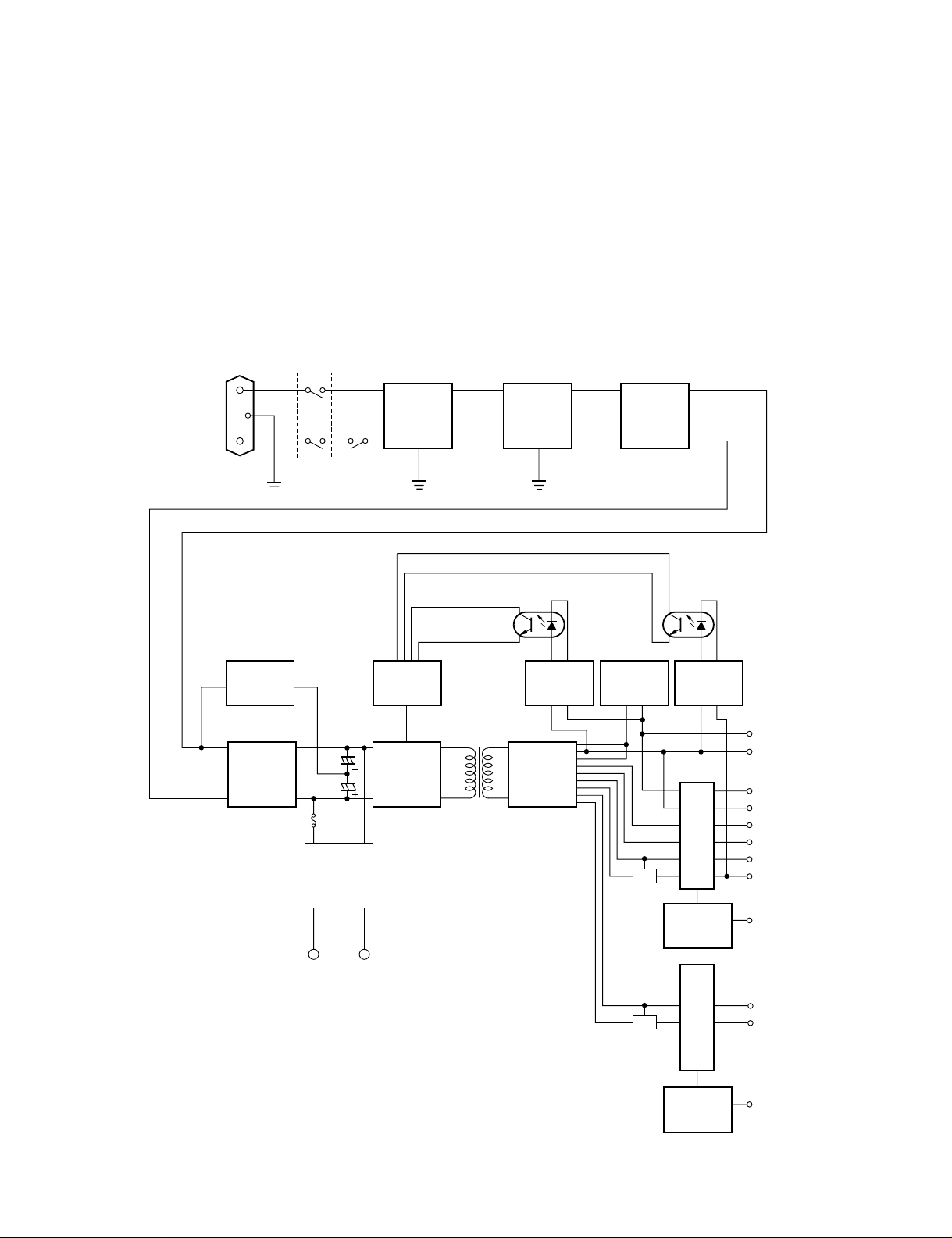
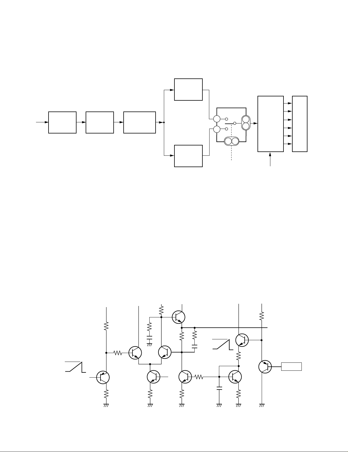
1. OUTLINE
The power supply circuit operates on AC as input and
outputs DC (+S6V, +6V, +10V, +12V, +15.5V) through
inverter after rectif ication and smoothing of the A C po wer .
ON/OFF function is provided for outputs other than +S6V
by the external signal. It is also capable of providing high
voltage output with inverter drive for halogen lamp. Fig.
1-1 shows the block diagram.
1-1. Block Diagram
2. DESCRIPTION ABOUT CIRCUIT OPERATION
2-1. Surge Absorber Circuit
The surge absorber circuit consists of protection element
(varistor) and spark gap on the pattern surface on the PC
board, making it possible to protect the power from being
destroyed by lighting stroke and impulse invaded from
external or from malfunction.
Inlet
N
L
Rectification
switching
circuit
Input
rectification
circuit
F002
Switch
Noise
filter
circuit
F001
Surge
absorber
circuit
125V
Primary
control
circuit
Inverter
circuit
flyback
Transformer
T001
Noise
filter
circuit
PC002
+6V output
detection
circuit
Secondary
rectification
smoothing
circuit
Rush
current
protection
circuit
+6V,+S6V
excesscurrent
protection
4TR
PC001
+6V,+S6V,
+15.5V
over-voltage
protection
Output ON/OFF
+S6V
+6V
+12V
circuit
+15.5V
High voltage output
315V
DV
Fig. 1-1 Block diagram
1-2
4TR
ON/OFF
control
circuit
circuit
Output ON/OFF
ON/OFF
control
circuit
ON/OFF
+10V
ON/OFF
2-2. Noise Filter Circuit
C012
C011
V
IN(AC)
SWITCH
(IC001)
C012
C011
V
IN(AC)
SWITCH
(IC001)
2-4. Smoothing/Rectifying Circuit
The noise filter circuit only protects the noise generated
by the power source from leaking out to AC line and from
entering of the external noise inside the power . This circuit
is effective for both normal and common noise.
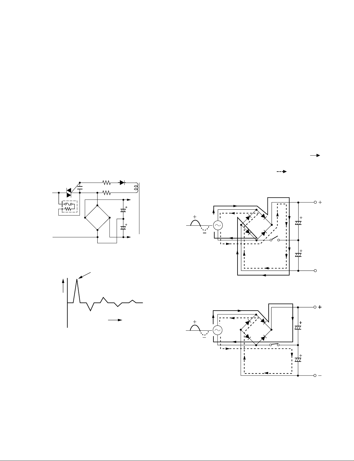
2-3. Rush Current Protection Circuit
When AC power is, via D001, rectified and directly applied to C011 and C012, rush current runs through C011
and C012 as shown in Fig. 1-3. The current degrades the
contact point of SW001. This rush current is controlled
by the circuit shown in Fig. 1-2, preventing the degradation of the contact point.
Before the power activation, there exists no induced voltage in T001. SCR001 is in the OFF state. Rectified AC
current runs through RF001 and charges C011 and C012.
T001
C012
C011
AC
AC
SCR001
RF001
~
+–
~
The input voltage of the unit is set to work in the range of
AC100 ~ 120V and AC220 ~ 240V. To keep the AC rectification output voltage in almost the constant level, the
voltage doubler rectification is employed for the AC100
~ 120V input and the bridge rectification for the AC220 ~
240V input. An exclusive IC is used to switch the voltage
doubler rectification and the bridge rectification. Figs. 14, 1-5 and 1-6 show the basic circuits.
When the switch is turned off, each of a positive and negative half-wave voltage of V
is charged to C012 and
IN (AC)
C011, and the bridge rectification voltage is developed
from the output terminal. On the other hand, when the
switch is turned on, a positive half-wave voltage of V
is charged to C012 through the circuit shown by
(AC)
and a negative half-wave voltage of V
IN (AC)
is charged to
IN
C011 through the circuit shown by . The voltage
doubler of the half-wave rectification voltage is developed
from the output terminal.
Fig. 1-2
Rush current
I
0
T
Fig. 1-3
With this, RF001 becomes charging resistance and is suppressed less than 30A. Then, when the charging voltage
of C011 and C012 becomes more than the activation
voltage, the inverter starts oscillation (activation) and the
voltage is generated in the T001. This voltage is used for
trigger voltage for SCR001, turns on the SCR001 and shortcircuits the RF001. As a result, the rectified current flows
into C011 and C012, eliminating the power loss by RF001
in the normal operation state.
Fig. 1-4 Bridge rectification (SW: OFF)
Fig. 1-5 Voltage doubler rectification (SW: ON)
1-3
The half-wave rectification for V
VDC
Q001
T001
N
P
N
S
N
C
Point B
R009
R010
C016
Q004
PC002
R018
R020
ZD003
6V
DC
D101
C018
is carried out by
IN (AC)
C and Di (D007) shown in the dotted line ----. When the
input voltage is low, the triac is turned on (voltage doubler
rectification) and when the input voltage high, the triac is
turned off (bridge rectification).
IN(AC)
V
Rectification switching circuit
(IC001)
C012
2-6. Primary Control Circuit
The control system employs automatic flyback system by
timing capacitor.
In the circuit diagram in Fig. 1-8, when power is turned
on, input voltage VDC is applied to B point. Voltage is
applied to Q001 gate via R009 and R010. Then Q001 is
activated. When Q001 is turned on, the drain current begins
to flow as shown in Fig. 1-7 and input voltage is applied
to NP winding.
Di
D007
C
Det. circuit
Latch circuit
SW
Rectification
C011
Fig. 1-6
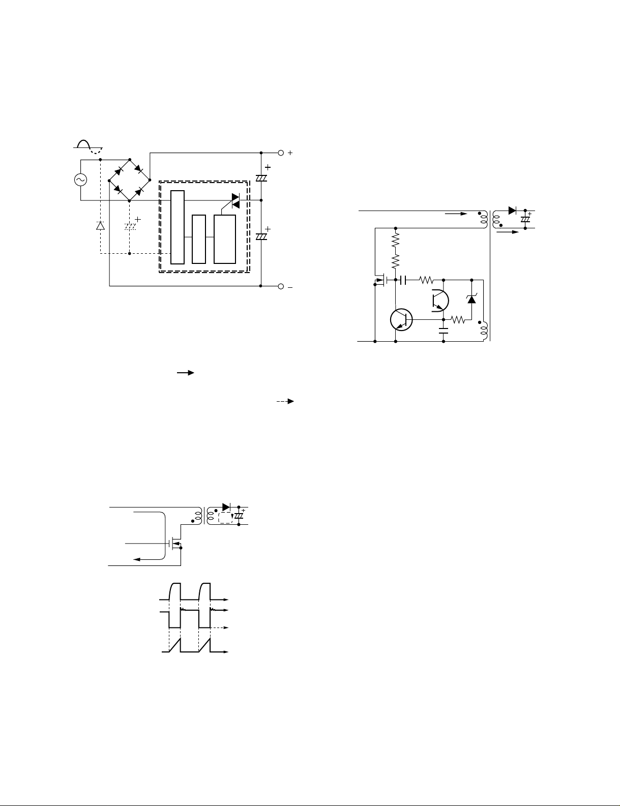
2-5. Inverter Circuit (Flyback)
The current indicated with to the converter transformer is turned on/off by the FET switch of Q001
operation. In the OFF state, the current indicated with
flows.
Signal is supplied to gate from the primary control circuit.
With this, Q001 starts switching operation.
Gate voltage, drain voltage, and current waveform of Q001
are shown in Fig. 1-7.
T001
P
N
Fig. 1-7
Q001
N
S
T
T
T
V
DC
Q001
VGS
0
Q001
VDS
0
Q001
ID
0
Fig. 1-8
The voltage V
= NC/NP x VDC is generated in the N
NC
winding and voltage is supplied to Q001 gate through R018
and C016. At the same time, C018 is charged through
ZD003 and R020.
When the electric potential of C018 rises up to VBE (Sat)
= approx. 0.7V, Q004 is turned on and Q001 is turned off.
That is, ON period of Q001 is determined by the time
constant of ZD003, R020 and C018. When Q001 becomes
off, the energy (flyback) accumulated in the transformer
T001 is output through D101. When this energy becomes
zero, D101 becomes off. For there exists a slight residual
energy in NS winding, by means of which voltage is
generated in the gate winding NC, which turns on the Q001
again to resume switching operation.
On the other hand, when the voltage output through D001
is rectified by the secondary rectifying/smoothing circuit,
when the voltage is detected by +6V detection circuit,
PC002 becomes on. This shortens the time constant to
charge C018. At the same time, the ON period of Q001 is
controlled and the output voltage (+6V) becomes stable.
C
1-4
2-7. Secondary Rectification & Smoothing
Circuit
2-9. +6V, +S6V, +15.5V Overvoltage
Protection Circuit
High-voltage applied to NP becomes, as mentioned previously, pulse by means of the switching operation and then
converted to low voltage at both ends of the secondary
side winding NS via T001 and is output after rectification/smoothing.
Q001
V
DS
+6V
A
I
0
B
0
+6V
B
A
T001
N
P
N
S
I
Fig. 1-9
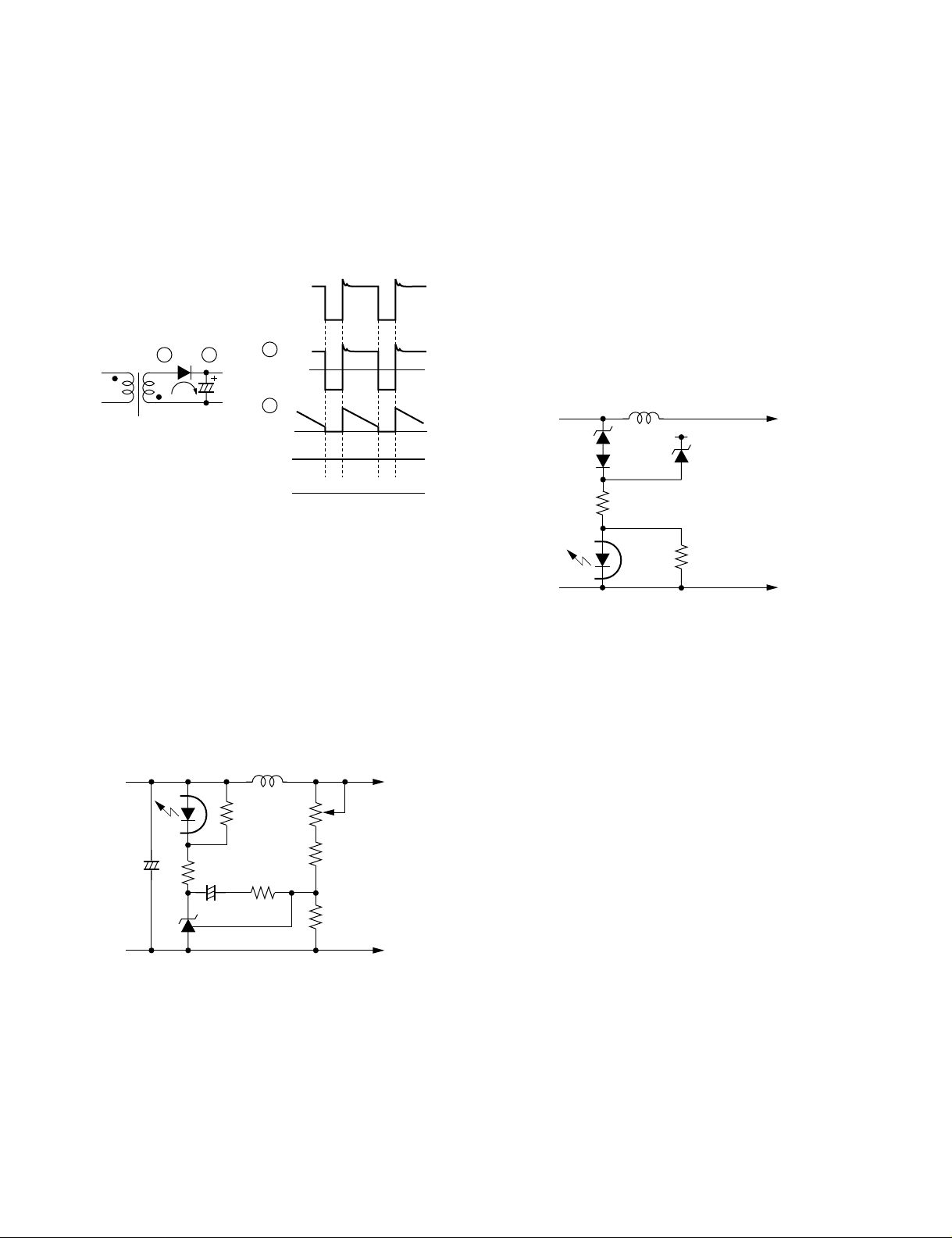
2-8. +6V Detection Circuit
As shown in Fig. 1-9, the overvoltage of +6V and +S6V
is detected by ZD101 and the overvoltage +15.5V is detected by ZD401.
When the overvoltage is detected, current flows to zener
diode, the current then flows to PC001. This is transferred
to the primary control circuit and trigger signal is given
to the gate of thyristor SCR002 to short-circuit the gate of
Q001. As a result, Q001 turns off and the oscillation stops.
The circuit is put to the latch mode. Therefore, no activation is possible even overvoltage state is released. Activation is made possible by reentry of input.
+S6V
+6V
PC001
ZD101
D102
R102
+15.5V
ZD401
R103
+6V voltage is divided by VR101, R113 and R114, it is
input to the gate of IC101 and then it is compared with
the reference voltage of that IC. This potential difference
flows into PC002 as current variation which is then
transferred to the primary side control circuit to control
output voltage.
IC101
L101
+S6V
VR101
R113
R114
G
PC002
K
A
G
Fig. 1-10
Fig. 1-11
1-5
2-10. +6V, +S6V Over Current Protection
Circuit
As shown in Fig. 1-12, this circuit detects the over current
by differential amplifier consisting of Q102 and Q103.
The reference voltage is produced by voltage division of
R105 and R106 using the +S6V as voltage source. This
voltage called VA (+S6V x R106/R105 + R106) is
compared with Voltage VB (Ioc x R108) generated by over
current. Q101 and Q102 turn on under the VA < VB
condition, by means of which the current is supplied to
PC001. This is transferred to the primary control circuit.
The rest of operation is the same as item 2-9.
To +15.5V
R104
PC001
R106
VA
Q101
Q102
R108
+S6V, +6V line
R105 R107
Q103
C103
VB
+S6V, +6V current
G
Fig. 1-12
2-11. Output ON/OFF Circuit
+15.5V and +10V outputs can be turned on/off by 4-terminal regulators IC401 and IC201. +5V and +6V outputs
can be turned on/off by POWER MOSS FET (Q106,
Q302). ON/OFF signal is given by the following ON/OFF
control circuit.
2-12. ON/OFF Control Circuit
This circuit controls the circuit of item 2-11, which delays the external signal by the integration circuits (R118
and C108) to send signals to each output circuit. Signal
level is TTL level. Each output becomes off at “L” and
becomes on at “H” approximately 300 ms later.
The ON/OFF signal of +12V is input from pin 2 of CN104
and turns Q302 ON/OFF passing through Q301 and PC101.
1-6

SECTION II
LAMP HIGH VOLTAGE
POWER SUPPLY CIRCUIT
2-1
1. LAMP HIGH VOLTAGE POWER SUPPLY
The lamp high voltage power supply receives a DC220 to
390V (primary side) from the system power supply and
provides a DC voltage (50 to 70VDC at ever turning on the
lamp) to turn on the lamp. Fig. 2-1 shows the block diagram.
CN701
(Pin 3)
220 - 390 V
STEPDOWN
TRANSFORM
CIRCUIT
DC
AUXILIARY
POWER SUPPLY
CIRCUIT
FULL BRIDGE
INVERTER
CIRCUIT
CONTROL
CIRCUIT
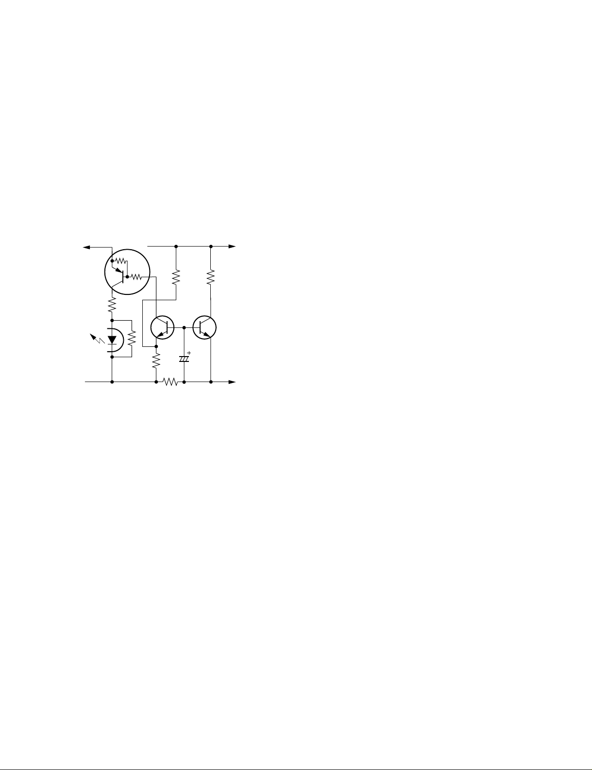
IGNITER
CIRCUIT
MISLIGHT
DETECT
CIRCUIT
(PHOTO TRANSISTOR)
LAMP
CN703
1 ON/OFF input
2 GND
3 Lamp off output ( – )
4 Lamp off output ( + )
The DC voltage is supplied to CN701 from the main power
supply unit through an interlock switch (S023). This voltage becomes AC input x 2Ö 2 (= 340V for AC120V input)
when the lamp is off. CN703 is a connector for the lamp on
control signal input and lamp off control signal output.
When +5V is applied to the ON/OFF input in the standby
on, Q702 FET transistor turns on, igniter develops a high
voltage pulse (13 to 18 kV), and the lamp starts to light up.
Fig. 2-1
The pulse continues until the lamp turns on (for about 1 to
2s.). But if the lamp does not turn on, the OFF output is
developed. Q702 goes of f after the lamp tur ned on, the igniter circuit stops the operation, and the DC50 to 70V is
applied to the lamp.
2-2

SECTION III
OPTICAL SYSTEM
3-1
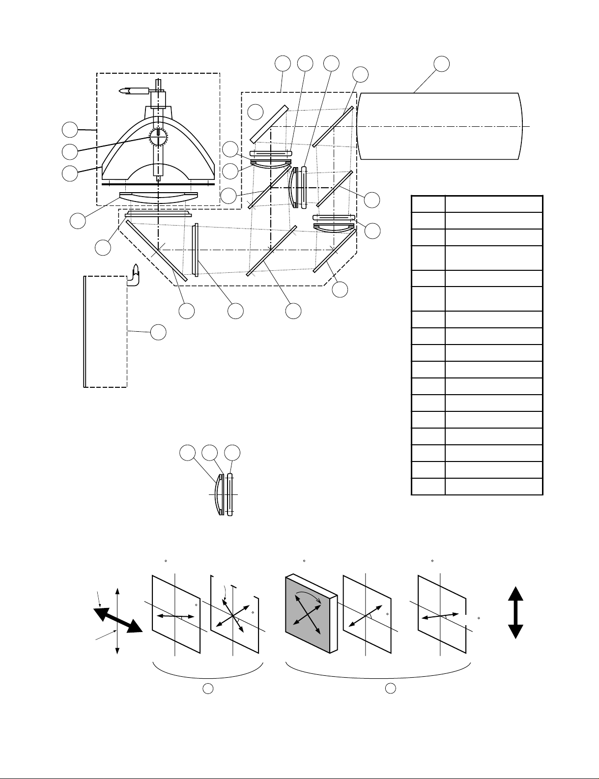
1. CONFIGURATION
No. Name Description
Lamp unit
Mirror
box unit
Projection
lens
17
16
15 Capacitor lens
14, 12 Multi-lens
13 Cold mirror
10a~
10f
3R
3G
3B
Metal halide
lamp
Elliptical
reflector
Dichroic m irror
5 Field lens
Phase difference
plate/ incidence
4
side polarized
plate
Liquid crystal
panel
(LCD)
1 Projection lens
Light source of the optical system. DC system,250W, short arc length 3mm.
To use light effectively in the tilt projection s ystem, the light axis is arra nged to face upwar d.
Elliptical reflecto r converges light emitted from the metal halide-lam p, thereby creating light
beams para llel with light axis and illumina ting the beams to the liquid crystal pane l.
Converges the parallel light beams from the reflector in direction of focal point and effectively
transmits the beams through 1.3 inch liquid crystal panel.
Multi-lens allows a circu lar beam light emitted from the light sourc e to illuminate the square
liquid crystal panel eve nly, thus providing projected pictures with les s brightness variatio n.
Visible light reflects at plane of incidence and goes to liquid crystal direction but infrared light
and ultraviolet light penetrate, thus preventing undesired harmful light components from
entering the liquid crystal panel.
Only red light component of white light emitted from the lamp transmits through 10a and
reflected by 10b, and e nters liquid crystal panel (R). At the sam e time, only green of green
and blue light components reflected is reflected by 10c and enters G-panel. While the blue
light component transm its through and enters B-pan el. Light transmitted through eac h liquid
crystal synthesized by the dichroic mirror 10f.
Light transmitted through liquid crystal panel is converged in direction of focal point and
effectively entered entranc e pupil of the projection len s.
Spectral characteristics for the dichroic mirror depend on polarization directions of the light
(P-polarization, S-po larization). To use the characteristics, a place the phas e difference plate
which possesses the characteristics to rotate the polarization direction of light by 45 degrees
is provided. When the spectral characteristic of S-polarization is important, the phase of Spolarization is converted so that it matches the transmission axis of the incidence side
polarization plate for the S-polarization light to pass the panel best.
On the other hand for the P-polarization, the phase is adjusted so that the P-polarization light
passes the panel best.
In this unit, when the S-polarization characteristic takes effective for the G-light component
and when the P-polarization characteristic takes effective for the R and B light components,
thus improving the light transmission amount projected from the optical unit and the color
reproduction characteristics.
Light exit side polarized plate and phase difference plate are put on the light exit plane.
Polarization direction of transmission light rotates by 90 degrees when no signal voltage is
applied, but a pola riz ed pla te has a char act eri stic whi ch sup press es the rot ati on when a vol tage
is applied, To effectively use this characteristic, polarized plates, phase difference of polarized
components transmitted through incidence side and exit side of which is 90 degrees, are
located. That is, p i c t u re i s di sp layed so th at l i gh t transmits t h ro ug h mos t (white) w h en no si g na l
voltage i s ap plied and the light transmits thro ug h l e as t (black) w he n a signal volt a ge i s ap plied.
Polarized light components transmitted through incidence side polarized plate is rotated by 45
degrees from Y axis in clockwise. This is to match aligning film of the liquid crystal panel for
increasing efficiency of the light transmissio n.
Phase difference p late rotates the ex it side p ola rized p late by 45 de gree s in c ounte rclock wise
direction (that is, in the light polarizing direction of the transmitting light) to obtain S-polarization
light. This operation is to increase effect of polarized screen because, generally speaking,
transmission axis of polarized screen has the same direction as that of S-polarization.
Projects pict ure s dis played on th e li quid cry stal at a wa ll , scr een, etc. Ligh t ax is of the pr oje cti on
lens is located at upper side of center of the liquid crystal panel because of a tilt projection
system employed. In a normal projection system, the projection screen is positioned at right
angle to the unit. In this case, the unit body will disturb for persons to see the screen in practice.
So, the projection will be directed upward, and this causes a trapezoidal distortion in the
picture. To prevent this, the tilt projection system which allows the users to see the pictures
projected without the trapezoidal distortion. (Figs. 3-4 and 3-5)
3-2
18
10
3
9
3
G
B
10
f
1
e
17
16
15
14
To Lamp
4
5
10
c
13
12
19
Fig. 3-1 Optical path diagram
10
10
d
3
R
10
b
a
No. Part name
1 Projection lens
3R Liquid crystal panel (red)
Liquid crystal panel
3G
(green)
3B Liquid crystal panel (blue)
Phase difference plate +
4
polarized plate
5 Field lens
9 Mirror box unit
10a-f Dichroic mirror
12 Multi-lens B
13 Cold mirror
14 Multi-lens A
15 Capacitor lens
P-polarization
light
S-polarization
light
Incidence
polarizing
direction
side
345
Phase
difference
plate
(45 rotation)
y
22.5
Incidence side
polarized
plate
S-polarization
light
P-polarization
light
45
Liquid
crystal
panel
(90 rotation)
Exit side
polarized
plate
45
x
4 3
Fig. 3-2 Polarizing direction at each part (G light components)
16 Elliptical reflector
17 Metal halide lamp
18 Lamp unit
19 High voltage supply
Phase
difference
plate
(45 rotation)
S-polarization
light
22.5
Exit side
polarizing
direction
3-3

P-polarization
light
S-polarization
light
Reflector
Incidence
polarizing
direction
Field lens
Lamp
Phase
difference
plate
(45 rotation)
side
Liquid crystal panel
y
22.5
Incidence side
polarized
plate
P-polarization
light
S-polarization
light
45
Liquid
crystal
panel
(90 rotation)
Exit side
polarized
plate
45
Phase
difference
plate
(45 rotation)
x
4 3
Fig. 3-3 Polarizing direction at each part (R/B light component)
Screen
Projection lens
S-polarization
light
22.5
Exit side
polarizing
direction
(a) General projection system (b) Picture by general projection system
Fig. 3-4 General projection system
Screen
Reflector
Projection lens
Liquid crystal panel
Field lens
Lamp
(a) Tilt projection system
Projection
lens light
axis
(b) Picture by tilt projection system
Fig. 3-5 Tilt projection system
3-4

SECTION IV
RGB DRIVE CIRCUIT
4-1
1. OUTLINE
This circuit is described using G process as an example
and composed of level shifter, gamma (g), black limiter,
inverted signal amplif ier, sample & hold circuit and liquid
crystal panel.
A block diagram of the drive circuit is shown in Fig. 4-1.
Normal
signal drive
Q971 – Q973
SW circuit
Q982
PD74HC4066A
Q983
CXA2504N
Level
shifter
Q945 – Q953 Q954 – Q963 Q965 – Q970
Gamma
circuit
Level shifter
black limiter
2. CIRCUIT DESCRIPTION
The following description will be given assuming that V
of transistor is 0.7V.
2-1. Level Shifter (Q945 – Q953)
This circuit is composed of the emitter follower Q945, full
feedback unit gain amplifier Q946 – Q950, and the current
source circuit of sub bright for Q951 – Q953. The circuit
operates to vary only the DC level of the input signal and
develops the signal with only the DC level shifted from the
input signal at Q949. The shift level is determined by the
current flowing into R976.
BE
signal drive
Q974 – Q980
Fig. 4-1
Liquid
crystal
panel
Inverted
1
4
5 13
2
3
Sample
and
hold circuit
Sample and hold pulse
When a triangular waveform of 2.3V – 3.6V shown in Fig.
4-2 is input, a triangular waveform of 3.0 – 4.3V appears at
the base of Q946. At the same time, a triangular wa veform
of approx. 3.0V – 4.3V also appears at the base of Q948.
Assuming the sub brightness adjustment voltage at Q953
is 1.83 VDC, a current of (1.83V – 0.7V)/(220 + 15) = 4.97
mA flows into Q951 and Q950, and this current also flows
into R976. Therefore, the emitter voltage of Q949 develops 1.06V higher than the base voltage of Q948 as shown
in the equation; 4.8 mA x 220W = 1.06V . And the triangular waveform of 4.06V – 5.36V appears at the emitter of
Q949.
3.6V
2.3V
Q945
R976
Q946
Q948
Q947
Fig. 4-2 Level shifter circuit
4-2
Q949
5.36V
4.06V
Q950
4.8 mA 4.8 mA
Q952
R978
220
Q951
R979
15
Q953
1.83VDC
2-2. Gamma (
gg
g) Circuit
gg
The circuit consists of a current source consisting of R983,
R984, Q954, full feedback amplifier Q955 – Q960, the gain
variation circuit Q961 – Q963 and R991. (The circuit including Q955 – Q963 is called the gamma circuit.)
A current of (12.7V – 0.7V)/(1.3 kW + 15W ) = 9.15 mA is
flown into the current source for Q954 and the same current is also flown into Q956 (Q947). At the same time, a
current of 9.15 mA x (15/20) = 6.9 mA is flown into Q960.
The followings are described referring to Fig. 4-3.
The signal from the level shifter is supplied to the base of
Q955. If the device elements and currents of Q955 and Q957
are exactly the same, the base state of Q955 is same as that
of Q957. However, Q955 and Q957 are not paired in their
characteristics, the actual base state will be different. The
base state of Q957 is described by referring to the triangular waveform of 4.06V – 5.36V.
When the base of Q963 develops 3.55 VDC, the emitter of
Q961 develops 4.25 VDC. In the signal area where the base
of Q963 is higher than 4.25V , the current of 7.7 mA is flo wn
into R988 because of Q961 turned off, and the emitter voltage of Q956 increases by amount of 1.7V, 7.7 mA x 220W
= 1.7V , from the base of Q957. As the base voltage of Q957
is close to 4.25V, Q961 turns on and the current is flown
into the collector of Q960 through R991.
When the base voltage of Q957 develops 4.06V, the current flowing into R991 is 2.8 mA, (4.25V – 4.06V)/68 =
2.8 mA. The current flowing into R998 decreases by that
amount and the voltage shifting amount also decreases by
the same amount, 2.8 mA x 220W = 0.62V. The operation
is shown in Fig. 4-4.
7.06V
4.06V
1.3k
15
5.36V
Q955
Q956
Q957
Q956Q954
5.36V
4.06V
9.15 mA 7.7 mA 0.5 mA
R988
220
Q960
Fig. 4-3 Gamma circuit
Emitter voltage
R991
68
Q956
5.14V
7.06V
Q961
4.25V
R1004
Q962
Q963
3.55 V
Q968
DC
Q957
Base voltage
5.36V
(4.24V)
4.06V
1.7V
Fig. 4-4 Gamma circuit operation
4-3
(5.94V)
5.76V
0.62V
5.14V
2-3. Level Shifter Circuit
(Q965 – Q968, R1044)
Q965 – Q967 works as a current source. Assuming that the
base voltage of Q965 is 1.76 VDC, the current 4.2 mA is
flown into Q967 and the same current also flown into Q968.
The current and R1044 make a voltage drop and only the
DC level is shifted.
2-4. Black Limiter (Q969, Q970)
The black limiter is a switching circuit and its operation is
as follows. When the base voltage of Q969 is higher than
that of Q970, Q969 turns on and when the base voltage of
Q969 is lower than that of Q970, Q969 turns off and Q970
turns on.
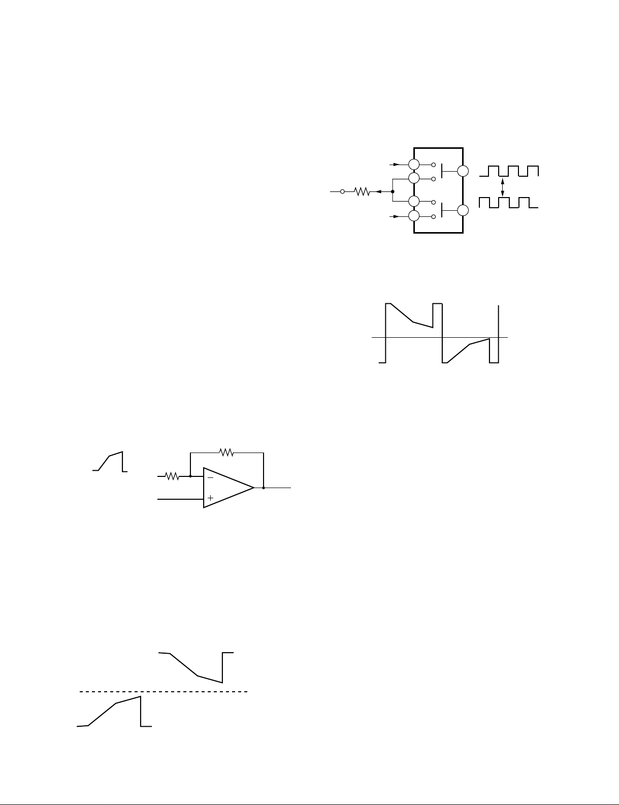
2-6. Switch Circuit (Q982 µPD74HC4066A)
The normal and inverted signal outputs are switched for
every horizontal and vertical period.
The signal is inverted for one horizontal period and then
further inverted for one vertical period.
Q982
Output
signal
TP905
Normal
input signal
R1025
Inverted
input signal
Fig. 4-7 SW circuit operation
1
2
3
4
13
Inverted
phase
5
The signal is inverted
for one horizontal period
and then further inverted
for one vertical period.
2-5. Inverted Signal Amplifiers
(Q974 – Q981)
• Q974, Q975: Emitter follower
• Q976 – Q978: Inverted signal amplifier
• Q979 – Q981: Emitter follower
The op. amplifier is composed of Q976 – Q978. Q977 base
accepts an inverted input and Q978 normal input. For easy
understanding of the op. amplifier, an op. amplif ier sho wn
in Fig. 4-5 will be refferred.
6V
R1017
4V
Q975 Emitter
Q978 Base
1k
7V
Fig. 4-5
The output of Q977 is 7V x (1 + R1018/R1017) – 4V =
10V , so 7V x (1 + R1018/R1017) – 6V = 8V is output. (The
constant of R1017 is assumed to 1 kW , in considering the
internal emitter resistor of Q975.)
Accordingly, the output shown in Fig. 4-6 is obtained.
R1018
1k
Q977
Collector
10V
8V
Fig. 4-8
4V
6V
7V
Q977
6V
Collector output
Q978 Base Input
4V
Fig. 4-6 Reverse output operation
10V
8V
(7V)
4-4
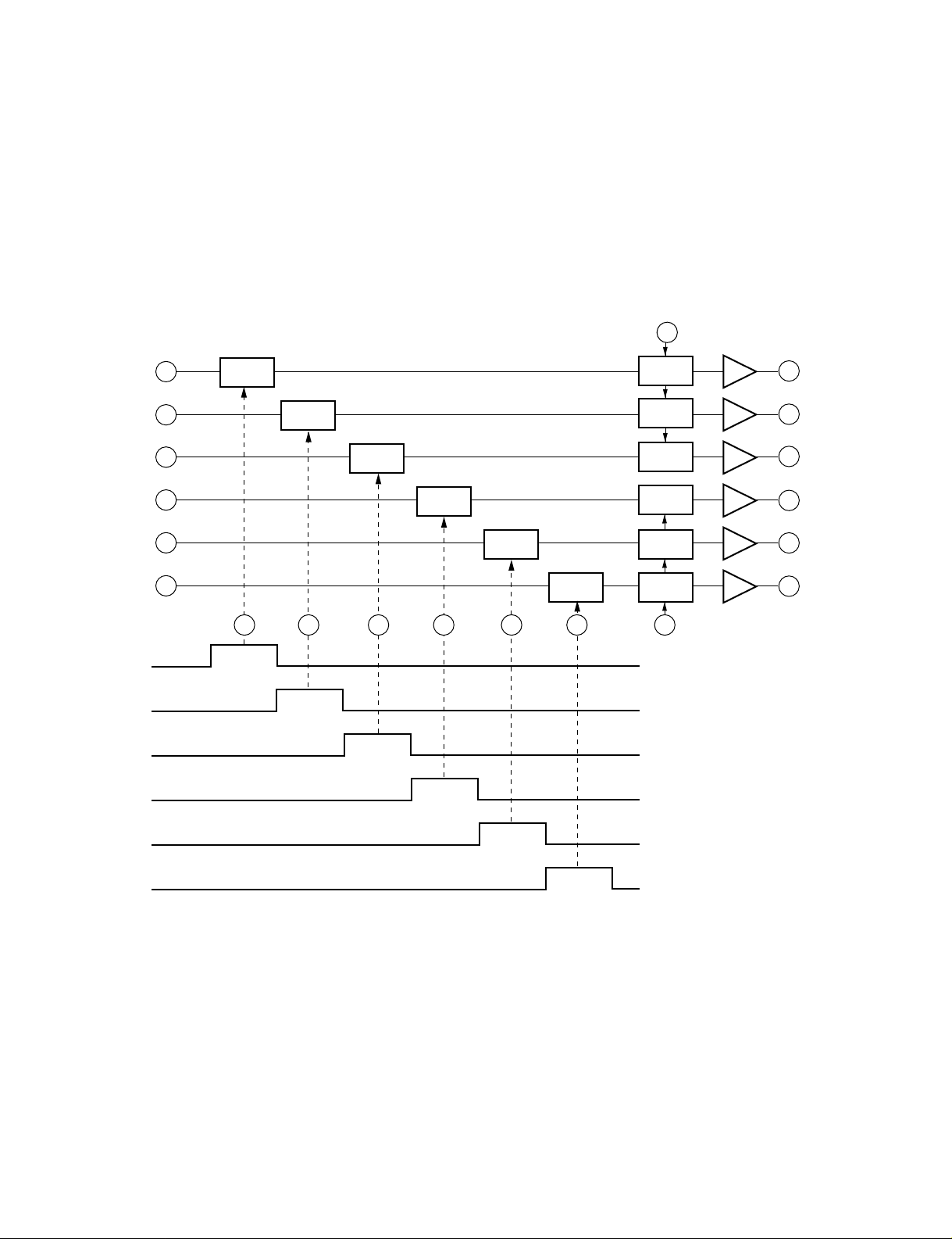
2-7. Sample & Hold Circuit
The block diagram of the circuit is shown in Fig. 4-10 and
its connection diagram is shown in Fig. 4-11. As shown in
the block diagram in Fig. 4-9, 6CH, each consisting of the
level shifter , S/H (sample and hold) and driv er circuits, are
contained in CXA2504N.
Sample & hold
16
S/H
Each sample & hold operation is carried out on pins 18,
19, 20, 1, 2 & 3 and the re-sample & hold operations for
6CH are carried out together on pins 21 and 40. This means
that the serial data is converted to the parallel data and the
LCD panel operation frequency is lowered.
Re-sample & hold
40
S/H
Drive
23
15 25
13 27
8 33
6 35
5
18
SH1
SH2
SH3
SH4
SH5
SH6
S/H
S/H
S/H
S/H
S/H S/H
19 20 1 2 321
S/H
S/H
S/H
S/H
The timings of pins 21
and 40 are the same
as that of SH6.
37
Fig. 4-9 Sample & hold operation
4-5
SH4
SH5
SH6
BIAS IN56
IN6
IN5
BIAS IN34
IN4
GND
GND
GND
Vcc1
IN3
BIAS IN12
IN2
IN1
I SH
SH1
SH2
SH3
1
2
3
4
Level shifter
S/H S/H
D/R
5
6
Level shifter
S/H S/H
D/R
7
8
Level shifter
S/H S/H
D/R
9
10
11
12
13
14
Level shifter
S/H S/H
D/R
15
16
Level shifter
S/H S/H
D/R
17
18
Level shifter
S/H S/H
D/R
19
20
Current
setting
Current
setting
40
SH8
39
I DR
38
BIAS OUT6
37
OUT6
BIAS OUT5
36
35
OUT5
34
BIAS OUT4
OUT4
33
Vcc2
32
31
GND
30
GND
29
GND
BIAS OUT3
28
27
OUT3
BIAS OUT1
26
25
OUT2
BIAS OUT1
24
23
OUT1
Vcc3
22
21
SH7
7 V
7 V
15.5V
DC
DC
22k
0.01
TP905
Fig. 4-10 CXA2504N block diagram
Sample & hold
pulse input
Sample & hold
pulse input
SH4
SH5
SH6
SH1
SH2
SH3
12 V
1
2
3
4
5
6
7
8
9
10
11
12
13
14
15
16
DC
17
18
19
20
Re-sample & hold
pulse input
SH8
40
1.2 V
DC
39
38
390k
7 V
7 V
390k
390k
1
DC
1
DC
1
37
36
35
34
33
32
0.01
47k
CH6 input
CH5 input
CH4 input
15.5V
To pin 7 of P903
To pin 5 of P903
To pin 3 of P903
31
30
29
7 V
DC
28
390k
7 V
390k
390k
1
DC
1
DC
1
27
26
25
7 V
24
23
22
21
SH7
CH3 input
CH2 input
CH1 input
5.0V
To pin 2 of P903
To pin 4 of P903
To pin 6 of P903
Re-Sample & hold
pulse input
Fig. 4-11 Peripheral circuit of sample & hold circuit
4-6
2-8. LCD Panel
The LCD panel uses the active matrix panel with 3.3 cm in
diagonal length and a built in driver made of the super thin
film multi-crystal silicone transistor. Use of 3 panels enables to display in full color mode. The pixels are arranged
in square form which is adequate for the data projection
use. This realizes to display figur es and characters clear ly.
Also, use of a high luminance screen employing the advanced on-chip black matrix and a built-in cross-talk free
circuit provides a high screen quality with less cross-talk.
The poly-silicone TFT high speed scanner is used and up/
down and left/right inv ersion function is provided. Furthermore, use of 5V system interface circuit realizes a low voltage consumption for the timing and control signals.
V shift register
(bidirectional scan)
Pre-charge
control circuit
Black frame
control circuit
2-8-1. Features
• Number of dots displayed: 519,000 dots in diagonal
length of 3.3 cm (1.3 type)
• High transparent ratio: 20%
• Built-in cross-talk free circuit
• High contrast ratio in normally white mode:
200 (Standard)
• Built-in H, V driver (Built-in input le vel con version circuit, 5V driving possible)
• Up/down and left/right inversion display function
2-8-2. Element component
• Number of dots: 832 (H) x 624 (V) = 519,168
• Active matrix panel with the driver using multi-crystal
silicone transistors
The block diagram of the LCD panel is shown in Fig. 4-12
and terminal description is in Table 4-1.
PSIG
1
Left-right/upper-lower
reverse control circuit
Input
signal
level
shifter
circuit
Black frame control circuit
H shift register (bidirectional scan)
13
14
15
17
9
20
19
21
22
18
12
11
10
8
23
HST
HCK1
HCK2
BLK
RGT
VST
VCK
PCG
DWN
ENB
MODE1
MODE2
MODE3
HV
DD
VV
DD
COM
polarity
Black frame
control circuit
V shift register
(bidirectional scan)
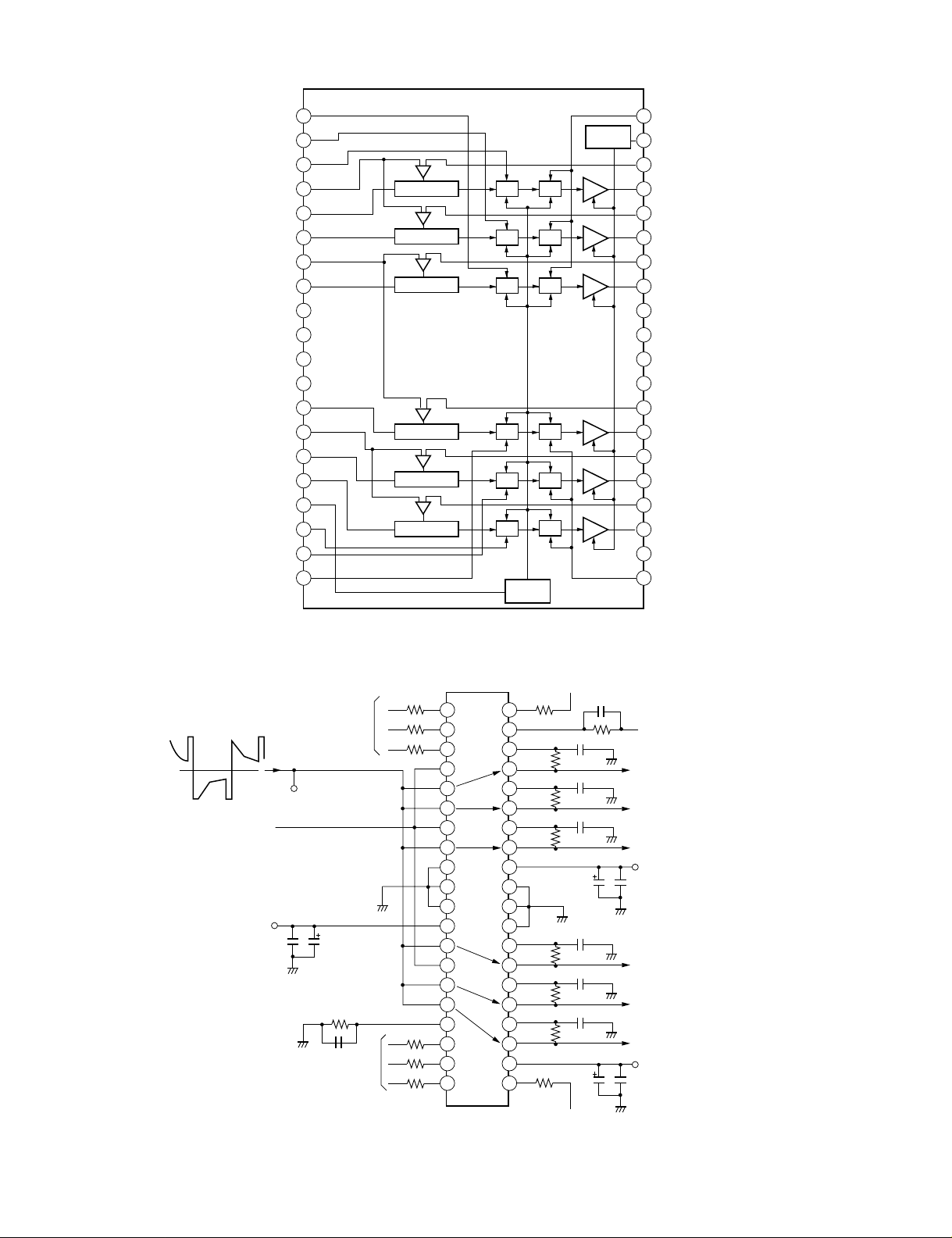
Fig. 4-12 Liquid crystal panel block diagram
4-7
16
24
VSS
SIG1
7
SIG2
5
SIG3
3
2
SIG4
4
SIG5
SIG6
6
COM
The liquid crystal panel is provided with a built in display
(
)
(
)
area variable circuit inside the liquid crystal panel. It is
possible to correspond with each signal of MAC16/SVGA/
VGA/PC98/NTSC/WIDE/PAL. The mode switching described above is carried out owing to the signal developed
at pins 10 to 12 of the display area switch input terminal as
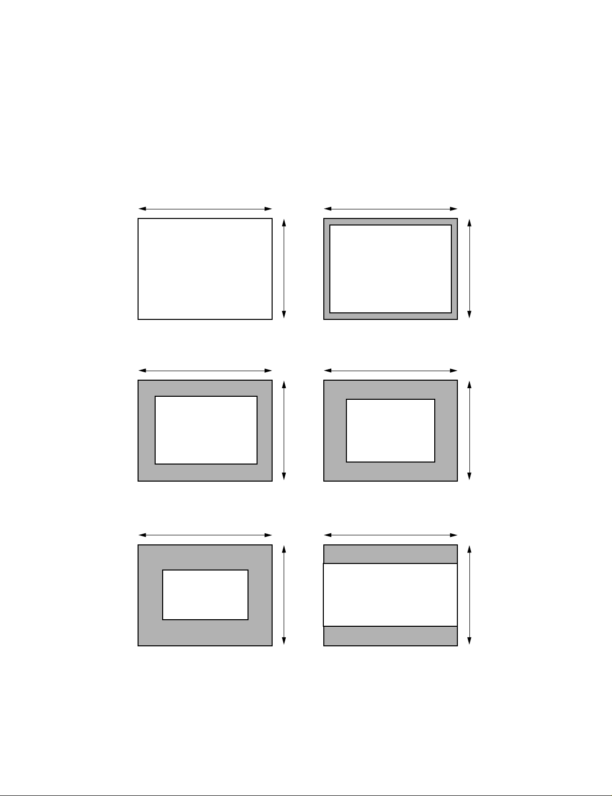
shown in Fig. 4-13. The area not displayed (shaded portions in Fig. 4-13) is written by PSIG signal of pin 1.
832
DISPLAY
AREA
832 x 624
Macintosh 16 MODE
(MODE1=L, MODE2=L, MODE3=L)
832
DISPLAY
AREA
762 x 572
PAL MODE
(MODE1=L, MODE2=H, MODE3=L)
624
624
832
DISPLAY
AREA
800 x 600
SVGA MODE
(MODE1=L, MODE2=L, MODE3=H)
832
DISPLAY
AREA
640 x 480
VGA/NTSC MODE
(MODE1=L, MODE2=H, MODE3=H)
624
624
832
DISPLAY
AREA
640 x 400
PC-98 MODE
MODE1=H, MODE2=L, MODE3=L
624
MODE1=H, MODE2=L, MODE3=H
832
DISPLAY
AREA
832 x 480
WIDE MODE
624
Fig. 4-13
4-8
Table 4-1 Liquid crystal panel terminal description
Pin
Symbol Description
No.
Uniformity improv ement sign al input term inal
1 PSIG
2SIG4
Video signal 4 input terminal to LCD pane l, 7V
center ± 4.5 V max.
11.5V
7V
2.5V
Pin
Symbol Description
No.
13 HST
Start pulse input term inal for H shift resistor
driving
14 HCK 1 Clo ck input termin al for H shift resistor dr iving
3 SIG 3 Video s ignal 3 input terminal to LC D panel 15 HCK2 Clock input term inal for H shift resis tor driving
4 SIG5 Video signal 5 input terminal to LCD pa nel 16 V
GND terminal for H, V drivers, G ND
SS
5 SIG2 Video signal 2 input terminal to LCD panel 17 BLK External frame display pulse input terminal
6 SIG6 Video signal 6 input termina l to LCD panel 18 ENB En able input te rminal fo r gate se lection puls e
7 SIG 1 Video s ignal 1 input terminal to LC D panel 19 VCK Clock inp ut terminal for V sh ift resistor driving
8HV
DD
Power supply inp ut terminal for H dr iver, 15.5V 20 VS T
Start pulse input term inal for V shift re sistor
driving
Driving dire ction input te rminal fo r H sh ift
9RGT
resistor (H: Normal direction, L: Reverse
21 PCG Uniformity improvement pulse input terminal
direction)
10 MODE3 Display area SW 3 input terminal 22 DWN
11 MODE2 Display area SW 2 input terminal 23 VV
12 MODE1 Display area SW 1 input terminal 24 COM
Driving dire ction input te rminal fo r V sh ift resist
or (H: Normal direction, L: Reverse direction)
Power supp ly input terminal fo r V driver, 15.5V
DD
Counter power supply voltage input terminal
for LCD panel, 6.6 V
DC
4-9

SECTION V
MICROCOMPUTER
5-1

1. SYSTEM OUTLINE
The system microcomputer has features as shown below.
In considering easy maintenance for specification modifi-
cation, etc. an external program ROM is employed. The
program is also developed in considering use of structured
notation, parts modularity, and multi filling system.
Major functions of the system microcomputer are as follows.
(1) System control
• Power reset process
• Nonvolatile memory control process
• Remote control reception process
• RS-232C transmission and reception process
• Status reading process
• On-screen display process
(2) Normal control
• Power ON/OFF
• Input switch
• Sound volume control UP/DOWN
• Menu UP/DOWN
• Mute ON/OFF
• Display ON/OFF
• Adjusting value reset
• Focus UP/DOWN
• Zoom UP/DOWN
(3) Adjustment control
• Video controls (high & low brightness ratio,
brightness, color density, tint, sharpness)
• Panel adjustments (V position, H position, phase,
clock)
• Projection adjustments (Front projection, front
projection with ceiling mount, rear projection, rear
projection with ceiling mount)
• Mode adjustments (Enlarge, wide, OSD mute, user
fixing)
• Adjustment data saving process
• Adjustment data default setting
(4) Adjustment control at shipping
• Video sub adjustments (RGB gain)
• Drive adjustments (each item)
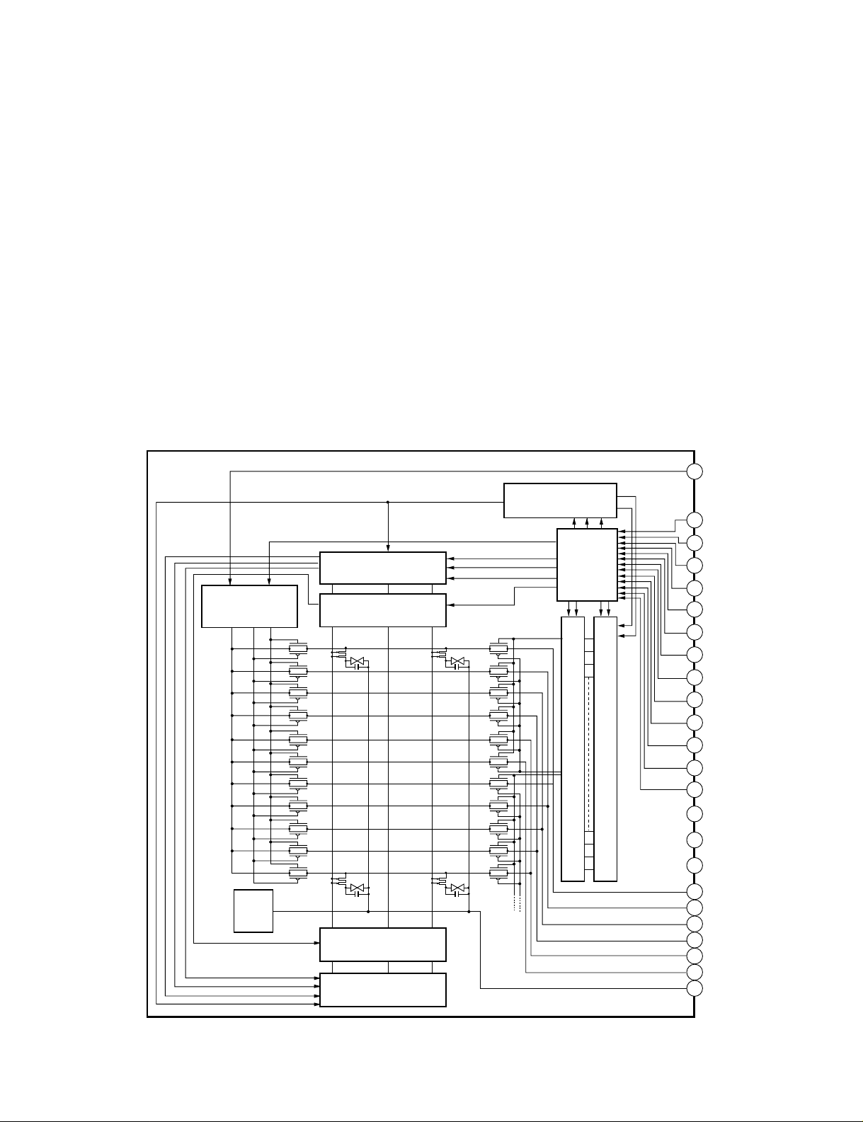
Fig. 5-1 shows the system block diagram.
5-2
Loading...