


TD62107P/BP/F
TOSHIBA BIPOLAR DIGITAL INTEGRATED CIRCUIT SILICON MONOLITHIC
TD62107P,TD62107BP,TD62107F
4CH HIGH−CURRENT DARLINGTON SINK DRIVER
The TD62107P / BP / F are high−voltage, high−current darlington drivers and enable inputs which can gate the outputs. All units feature integral clamp diodes for switching inductive loads.
The TD62107P / BP / F have a wide supply voltage range and all input are compatible with TTL and 5−V CMOS.
Application include relay, hammer, lamp and stepping moter drivers.
Please observe the thermal condition for using.
FEATURES
l Output current (single output) 750mA (MAX)
l High sustaining voltage output 80 V MIN. (TD62107BP) 45 V MIN. (TD62107P) 35 V MIN. (TD62107F)
lOutput clamp diodes
lEnable inputs E1, E2
lWide supply voltage range VCC = 4.75~17 V
lInput compatible with TTL and 5−V CMOS
lGND terminal = heat sink
l |
Package type−P, BP |
: DIP−16pin |
|
|
|
Package type−F |
: HSOP−16pin |
|
|
l |
|
Weight |
||
|
|
|
|
DIP16−P−300−2.54A : 1.11 g (Typ.) |
PIN CONNECTION (TOP VIEW) |
|
HSOP16−P−300−1.00 : 0.50 g (Typ.) |
||
|
|
|||
|
TD62107P / TD62107BP |
TD62107F |
||
1 |
2001-07-16 |
|
|
|
|
TD62107P/BP/F |
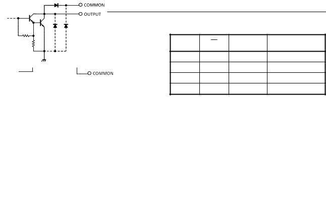
SCHEMATICS (EACH DRIVER) |
TRUTH TABLE |
|
|
|
|
E1 |
E2 |
I1 ~ I4 |
O1~O4 |
|
L |
L |
L or H |
Disable OFF |
|
L |
H |
L or H |
Disable OFF |
|
H |
L |
L or H |
Enable In |
|
H |
H |
L or H |
Disable OFF |
In = I1 ~ I4
INPUT EQUIVALENT CIRCUIT |
OUTPUT EQUIVALENT CIRCUIT |
Note: |
The input and output parasitic diodes cannot be |
|
used as clamp diodes. |
MAXIMUM RATINGS (Ta = 25°C)
CHARACTERISTIC |
|
SYMBOL |
RATING |
UNIT |
|
|
|
|
|
|
|
Supply Voltage |
|
VCC |
−0.5~17 |
V |
|
|
P |
|
−0.5~45 |
|
|
Output Sustaining Voltage |
|
VCE (SUS) |
|
V |
|
BP |
−0.5~80 |
||||
|
F |
|
−0.5~35 |
|
|
|
|
|
|
|
|
Output Current |
|
IOUT |
750 |
mA |
|
Input Voltage |
|
VIN |
−0.5~VCC + 0.5 |
V |
|
|
P |
|
45 |
|
|
Clamp Diode Reverse Voltage |
|
VR |
|
V |
|
BP |
80 |
||||
|
F |
|
35 |
|
|
|
|
|
|
|
|
Clamp Diode Forword Current |
P, F |
IF |
500 |
mA |
|
|
|
||||
BP |
750 |
||||
|
|
|
|||
|
|
|
|
|
|
Power Dissipation |
P, BP |
PD |
2.7 (Note 1) |
W |
|
|
|
||||
F |
1.4 (Note 2) |
||||
|
|
|
|||
|
|
|
|
|
|
Operating Temperature |
|
Topr |
−40~85 |
°C |
|
Storage Temperature |
|
Tstg |
−55~150 |
°C |
Note 1: On Glass Epoxy PCB (50 × 50 × 1.6 mm Cu 50%)
Note 2: On Glass Epoxy PCB (60 × 30 × 1.6 mm Cu 30%)
2 |
2001-07-16 |

TD62107P/BP/F
RECOMMENDED OPERATING CONDITIONS (Ta = −40~85°C)
CHARACTERISTIC |
SYMBOL |
CONDITION |
|
MIN |
TYP. |
MAX |
UNIT |
|||
|
|
|
|
|
|
|
|
|
|
|
Supply Voltage |
|
VCC |
|
|
|
4.75 |
― |
15 |
V |
|
|
P |
|
|
|
|
0 |
― |
45 |
|
|
Output Sustaining |
|
VCE (SUS) |
|
|
|
|
|
|
V |
|
BP |
|
|
|
0 |
― |
80 |
||||
Voltage |
|
|
|
|||||||
|
F |
|
|
|
|
0 |
― |
35 |
|
|
|
|
|
|
|
|
|
|
|
||
|
P, F |
|
Tpw = 25ms, Duty = 75%, 1 Circuit |
0 |
― |
500 |
|
|||
Output Current |
BP |
IOUT |
Tpw = 25ms, Duty = 10%, 4 Circuits |
0 |
― |
750 |
mA |
|||
P, BP |
Tpw = 25ms, 4 Circuits |
|
Duty = 30% |
0 |
― |
400 |
||||
|
|
|
|
|||||||
|
|
|
|
|
|
|
|
|
||
|
F |
|
|
Duty = 40% |
― |
― |
300 |
|
||
|
|
|
|
|
||||||
|
|
|
|
|
|
|
|
|
|
|
Input Voltage |
|
VIN |
|
|
|
0 |
― |
VCC |
V |
|
|
P |
|
|
|
|
― |
― |
45 |
|
|
Clamp Diode |
|
VR |
|
|
|
|
|
|
V |
|
BP |
|
|
|
― |
― |
80 |
||||
ReverseVoltage |
|
|
|
|||||||
|
F |
|
|
|
|
― |
― |
35 |
|
|
|
|
|
|
|
|
|
|
|
|
|
Clamp Diode |
P, F |
IF |
|
|
|
― |
― |
500 |
mA |
|
Forward Current |
|
|
|
|
|
|
|
|||
BP |
|
|
|
― |
― |
750 |
||||
|
|
|
|
|
|
|||||
|
|
|
|
|
|
|
|
|
|
|
Power Dissipation |
B, BP |
PD |
|
|
|
― |
― |
1.0 |
W |
|
|
|
|
|
|
|
|
||||
F |
Ta = 85°C |
(Note) |
― |
― |
0.7 |
|||||
|
|
|
||||||||
|
|
|
|
|
|
|
|
|
|
|
Note: On Glass Epoxy PCB (60 × 30 × 1.6 mm Cu 30%)
3 |
2001-07-16 |
 Loading...