


www.DataSheet4U.com
TB6556F/FG
TOSHIBA Bi-CMOS Integrated Circuit Silicon Monolithic
TB6556F/FG
3-Phase Full-Wave Sine-Wave PWM Brushless Motor Controller
Features
•Sine-wave PWM control
•Built-in triangular-wave generator (carrier cycle = fosc/252 (Hz))
•Built-in lead angle control function (0° to 58° in 32 steps) External setting/automatic internal setting
•Built-in dead time function (setting 2.6 µs or 3.8 µs)
•Supports bootstrap circuit
•Overcurrent protection signal input pin
• |
Built-in regulator (Vrefout = 5 V (typ.), 30 mA (max)) |
Weight: 0.33 g (typ.) |
• |
Operating supply voltage range: VCC = 6 V to 10 V |
|
DataShe
DataSheet4U.com
TB6556FG:
TB6556FG is a Pb-free product.
The following conditions apply to solderability: *Solderability
1.Use of Sn-63Pb solder bath *solder bath temperature = 230˚C *dipping time = 5 seconds *number of times = once
*use of R-type flux
2.Use of Sn-3.0Ag-0.5Cu solder bath *solder bath temperature = 245˚C *dipping time = 5 seconds
*the number of times = once *use of R-type flux
DataSheet4U.com
1 |
2005-01-19 |
DataSheet4U.com

.DataSheet4U |
et4U |
|
. |
|
com |
com |
|
|
|
|
|
TB6556F/FG |
|
|
|
|
|
|
|
Block Diagram |
|
|
|
|
|
|
Gin |
Gout |
PH |
LPF |
LA |
UL |
LL |
24 |
25 |
26 |
27 |
28 |
30 |
29 |
com.DataSheet4U
|
|
|
|
Peak hold |
+ |
Filter |
|
Upper limit |
|
|
|
|
|
|
|
|
|
|
|
|
|||
|
|
|
|
|
|
|
|
|
|
||
|
|
|
|
|
|
|
|
Lower limit |
|
|
|
Xin |
14 |
System clock |
|
|
|
|
|
6-bit triangular |
|
|
|
Xout |
15 |
generator |
|
|
|
|
|
wave generator |
|
|
|
|
|
5-bit AD |
|
|
|
|
|
|
|
||
HU |
21 |
|
|
|
|
|
|
|
Phase U |
Comparator |
|
HV |
20 |
Position detector |
|
Counter |
|
|
|
|
|
|
|
HW |
19 |
|
|
|
|
Output |
|
Data |
Phase V |
Comparator |
|
|
|
|
|
|
|
waveform |
.DataSheet4U |
select |
|
|
|
|
|
Internal |
|
Phase |
|
generator |
|
|
|
||
GND |
13 |
|
|
|
|
Charger |
and |
||||
Ve |
2 |
reference |
matching |
|
|
|
|
Phase W |
Comparator |
|
|
|
|
voltage |
|
|
|
|
|
|
|||
VCC |
|
|
|
|
|
|
|
|
|
|
|
1 |
Regulator |
|
|
|
|
|
|
|
|
|
|
|
|
|
|
|
|
|
|
|
|
120/180 |
Switching |
|
|
|
|
|
|
|
|
|
|
|
120°/180° |
Vrefout |
23 |
|
Rotating |
|
|
com |
Comparator |
PWM |
|
gate block |
|
FG |
|
|
|
protection |
|||||||
|
|
Power-on |
direction |
|
|
|
|
HU |
|
on/off |
|
|
|
reset |
|
|
|
|
|
|
|
|
|
|
|
|
|
|
|
|
|
HV |
|
|
|
RES |
11 |
|
|
|
|
|
|
|
120°- |
|
|
|
|
|
|
|
|
|
HW |
|
|||
|
|
|
|
|
|
|
|
|
turn-on |
|
|
Idc |
3 |
|
|
ST/SP |
|
|
|
|
|
matrix |
|
CW/CCW
CW/CCW |
18 |
Protection |
ERR |
|
|
& |
GB |
SS |
22 |
reset |
|
FG |
17 |
|
|
EV |
16 |
|
|
Setting dead time
10 Td
 9 U
9 U  6 X
6 X
 8 V
8 V  5 Y
5 Y
 7 W
7 W  4 Z
4 Z
12 OS
2 |
2005-01-19 |
com.DataSheet4U.www
DataShe

www.DataSheet4U.com
|
|
|
|
|
|
|
|
|
|
|
|
|
|
|
|
|
TB6556F/FG |
||
|
|
|
|
|
|
|
|
|
|
|
|
|
|
|
|
|
|||
|
|
|
|
|
|
|
|
|
|
|
|
|
|
|
|
|
|||
|
|
|
|
|
|
|
|
|
|
|
|
|
|
|
|
|
|||
|
|
|
|
|
|
|
|
|
|
|
|
|
|
|
|
|
|
|
|
|
Pin Description |
|
|
|
|
|
|
||||||||||||
|
|
|
|
|
|
|
|
|
|
|
|
|
|
|
|
||||
|
|
|
|
|
Pin No. |
|
|
|
Symbol |
Description |
|
Remarks |
|
|
|
||||
|
|
|
|
|
|
|
|
|
|
|
|
|
|
||||||
|
|
|
|
|
21 |
|
|
|
|
|
HU |
Positional signal input pin U |
When positional signal is HHH or LLL, gate block protection operates. |
|
|
||||
|
|
|
|
|
|
|
|
|
|
|
|
|
|
|
|
|
|||
|
|
|
|
|
20 |
|
|
|
|
|
HV |
Positional signal input pin V |
|
|
|
||||
|
|
|
|
|
|
|
|
With built-in pull-up resistor, built-in digital filter ( − 500 ns) |
|
||||||||||
|
|
|
|
|
19 |
|
|
|
|
|
HW |
Positional signal input pin W |
|
|
|
|
|||
|
|
|
|
|
|
|
|
|
|
|
|
||||||||
|
|
|
|
|
18 |
|
|
|
CW/CCW |
Rotation direction signal input |
L: Forward |
|
|
|
|||||
|
|
|
|
|
|
|
|
|
|
|
|
|
|
pin |
|
H: Reverse |
|
|
|
|
|
|
|
|
|
|
|
|
|
|
|
|
|
|
|
L: Reset (output is non-active) |
|
|
|
|
|
11 |
|
|
|
|
|
RES |
Reset-signal-input pin |
|
operation/halt operation, also used for gate protection, |
|
|||||||
|
|
|
|
|
|
|
|
|
|
|
|
|
|
|
|
built-in pull-up resistor |
|
|
|
|
|
|
|
|
|
|
|
|
|
|
|
|
|
|
|||||
|
|
|
|
|
2 |
|
|
|
|
|
Ve |
Voltage command signal |
|
With built-in pull-down resistor |
|
|
|
||
|
|
|
|
|
24 |
|
|
|
|
|
Gin |
Gain setting |
|
Idc signal level at a gain that optimizes the LA |
|
|
|
||
|
|
|
|
|
25 |
|
|
|
|
|
Gout |
|
|
|
|
||||
|
|
|
|
|
|
|
|
|
|
|
|
|
|||||||
|
|
|
|
|
26 |
|
|
|
|
|
PH |
Peak hold |
|
Connect the peak-hold capacitor and discharge resistor to GND, parallel |
|
|
|||
|
|
|
|
|
|
|
|
to each other |
|
|
|
||||||||
|
|
|
|
|
|
|
|
|
|
|
|
|
|
|
|
|
|
|
|
|
|
|
|
|
27 |
|
|
|
|
|
LPF |
RC low-pass filter |
|
Connect the low-pass filter capacitor (built-in 100 kΩ resistor) |
|
|
|||
|
|
|
|
|
|
|
|
|
|
|
|
|
|
|
|
|
|
|
|
|
|
|
|
|
28 |
|
|
|
|
|
LA |
Lead angle setting signal |
|
Sets 0° to 58° in 32 steps |
|
|
|
||
|
|
|
|
|
|
|
input pin |
|
|
|
|
||||||||
|
|
|
|
|
|
|
|
|
|
|
|
|
|
|
|
|
|
|
|
|
|
|
|
|
|
|
|
|
|
|
|
|
|
|
|||||
|
|
|
|
|
29 |
|
|
|
|
|
LL |
Lower limit for LA |
|
Set lower limit for LA (LL = 0 V to 5.0 V) |
|
|
|
||
|
|
|
|
|
|
|
|
|
|
|
|
|
|
|
|||||
|
|
|
|
|
30 |
|
|
|
|
|
UL |
Upper limit for LA |
|
Set upper limit for LA (UL = 0 V to 5.0 V) |
|
|
|
||
|
|
|
|
|
|
|
|
|
|
|
|
|
|
|
|
|
|
|
|
|
|
|
|
|
12 |
|
|
|
|
|
OS |
Inputs output logic select |
|
L: Active LOW |
|
|
|
||
|
|
|
|
|
|
|
signal |
|
H: Active HIGH |
|
|
|
|||||||
|
|
|
|
|
|
|
|
|
|
|
|
|
|
|
|
|
|
||
|
|
|
|
|
|
|
|
|
|
|
|
|
|
|
|
|
|
|
|
et4U.com |
|
|
|
|
|
|
|
|
|
|
|
|
|
Inputs overcurrent protection |
Inputs DC link current. |
|
|
DataShe |
|
|
|
|
|
3 |
|
|
|
|
|
Idc |
Reference voltage: 0.5 V |
|
|
||||||
|
|
|
|
|
|
|
signal |
|
|
|
|||||||||
|
|
|
|
|
|
|
|
|
|
|
|
|
|
|
With built-in filter ( 1 µs), built-in digital filter ( − |
1 µs) |
|
||
|
|
|
|
|
14 |
|
|
|
|
|
Xin |
Inputs clock signal |
|
DataSheet4U.com |
|
|
|
||
|
|
|
|
|
|
|
|
|
|
|
|
|
|
|
|
With built-in feedback resistor |
|
|
|
|
|
|
|
|
15 |
|
|
|
|
|
Xout |
Outputs clock signal |
|
|
|
|
|||
|
|
|
|
|
|
|
|
|
|
|
|
||||||||
|
|
|
|
|
23 |
|
|
|
|
Vrefout |
Outputs reference voltage |
|
5 V (typ.), 30 mA (max) |
|
|
|
|||
|
|
|
|
|
|
signal |
|
|
|
|
|||||||||
|
|
|
|
|
17 |
|
|
|
|
|
FG |
FG signal output pin |
|
Outputs 3 PPR of positional signal |
|
|
|
||
|
|
|
|
|
|
|
|
|
|
|
|
|
|
|
|
|
|
|
|
|
|
|
|
|
16 |
|
|
|
|
|
REV |
Reverse rotation detection |
|
Detects reverse rotation. |
|
|
|
||
|
|
|
|
|
|
|
signal |
|
|
|
|
||||||||
|
|
|
|
|
|
|
|
|
|
|
|
|
|
|
|
|
|
|
|
|
|
|
|
|
|
|
|
|
|
|
|
|
|
|
|||||
|
|
|
|
|
9 |
|
|
|
|
|
U |
Outputs turn-on signal |
|
|
|
|
|
||
|
|
|
|
|
|
|
|
|
|
|
|
|
|
|
|||||
|
|
|
|
|
8 |
|
|
|
|
|
V |
Outputs turn-on signal |
|
|
|
|
|
||
|
|
|
|
|
|
|
|
|
|
|
|
|
|
|
|||||
|
|
|
|
|
7 |
|
|
|
|
|
W |
Outputs turn-on signal |
|
Select active HIGH or active LOW using the output logic select pin. |
|
|
|||
|
|
|
|
|
|
|
|
|
|
|
|
|
|
|
|
|
|||
|
|
|
|
|
6 |
|
|
|
|
|
X |
Outputs turn-on signal |
|
|
|
||||
|
|
|
|
|
|
|
|
|
|
|
|
||||||||
|
|
|
|
|
|
|
|
|
|
|
|
|
|
|
|||||
|
|
|
|
|
5 |
|
|
|
|
|
Y |
Outputs turn-on signal |
|
|
|
|
|
||
|
|
|
|
|
|
|
|
|
|
|
|
|
|
|
|||||
|
|
|
|
|
4 |
|
|
|
|
|
Z |
Outputs turn-on signal |
|
|
|
|
|
||
|
|
|
|
|
|
|
|
|
|
|
|
|
|
|
|||||
|
|
|
|
|
1 |
|
|
|
|
|
VCC |
Power supply voltage pin |
|
VCC = 6 to 10 V |
|
|
|
||
|
|
|
|
|
10 |
|
|
|
|
|
Td |
Inputs setting dead time |
|
L: 3.8 µs, H or OPEN: 1.9 µs |
|
|
|
||
|
|
|
|
|
|
|
|
|
|
|
|
|
|||||||
|
|
|
|
|
22 |
|
|
|
|
|
SS |
120°/180° select signal |
|
L: 120° turn-on mode, H or OPEN: 180° turn-on mode |
|
|
|||
|
|
|
|
|
|
|
|
|
|
|
|
|
|
|
|||||
|
|
|
|
|
13 |
|
|
|
|
|
GND |
Ground pin |
|
|
|
|
|
||
|
|
|
|
|
|
|
|
|
|
|
|
|
|
|
|
|
|
|
|
DataSheet4U.com
3 |
2005-01-19 |
DataSheet4U.com

www.DataSheet4U.com
Input/Output Equivalent Circuits
Pin Description |
Symbol |
Input/Output Signal |
|
|
|
Digital |
|
Positional signal input pin U |
HU |
With Schmitt trigger |
|
Hysteresis 300 mV (typ.) |
|||
Positional signal input pin V |
HV |
||
Digital filter: 500 ns (typ.) |
|||
Positional signal input pin W |
HW |
||
|
|||
|
|
L: 0.8 V (max) |
|
|
|
H: Vrefout − 1 V (min) |
Forward/reverse switching |
Digital |
input pin |
CW/CCW |
|
|
L: Forward (CW) |
L: 0.8 V (max) |
H: Reverse (CCW) |
H: Vrefout − 1 V (min) |
.com |
Reset input |
|
Digital |
|
RES |
|
|
et4U |
L: Stops operation (reset) |
L: 0.8 V (max) |
|
|
H: Operates |
|
H: Vrefout − 1 V (min) |
DataSheet4U.com
|
Digital |
120°/180° select signal |
With Schmitt trigger |
SS |
Hysteresis: 300 mV (typ.) |
L: 120° turn-on mode |
|
H: 180° turn-on mode |
L: 0.8 V (max) |
(OPEN) |
H: Vrefout − 1 V (min) |
Voltage command signal |
|
Analog |
|
|
|
1.0 V < Ve ≤ 2.1 V |
Ve |
Input voltage range 0 to 5.4 V |
Refresh operation |
||
(X, Y, Z pins: ON duty of |
|
Input voltage of 5.4 V or higher is |
|
clipped to 5.4 V. |
|
8%) |
|
|
|
|
TB6556F/FG
Input/Output Internal Circuit
Vrefout Vrefout
 200 kΩ
2.0 kΩ
Vrefout Vrefout
 100 kΩ
2.0 kΩ
Vrefout Vrefout
 100 kΩ
2.0 kΩ
Vrefout Vrefout
 200 kΩ
2.0 kΩ
VCC
100 Ω
 150 kΩ
DataShe
DataSheet4U.com
4 |
2005-01-19 |
DataSheet4U.com

www.DataSheet4U.com
|
|
|
|
|
TB6556F/FG |
|
Pin Description |
Symbol |
Input/Output Signal |
Input/Output Internal Circuit |
|
|
|
|
When LA is fixed externally, connect |
|
|
|
|
|
LL to GND and UL to Vrefout, and then |
VCC |
|
|
|
|
input the setting voltage to the LA pin. |
|
|
|
Lead angle setting signal |
|
Input voltage range: 0 V to 5.0 V |
|
|
|
input pin |
|
|
|
|
|
|
(Vrefout) |
100 Ω |
|
|
|
0 V: 0° |
LA |
|
||
|
Input voltage of Vrefout or higher is |
|
|
||
|
|
kΩ |
|
||
|
5 V: 58° |
|
|
||
|
(5-bit AD) |
|
clipped to Vrefout. |
200 |
Automatic LA |
|
|
|
When LA is fixed automatically, open |
||
|
|
|
|
circuit |
|
|
|
|
the LA pin. In this state, the LA pin is |
|
|
|
|
|
used only for confirmation of LA width. |
|
|
|
|
|
|
VCC |
VCC |
|
|
|
Non-inverted amplifier |
100 Ω |
|
|
Gain setting signal input |
Gin |
25 dB (max) |
|
|
|
Gout output voltage |
Gin |
Gout |
||
|
(LA setting) |
Gout |
|
||
|
LOW: GND |
|
|
||
|
|
|
HIGH: VCC − 1.7 V |
|
|
|
|
|
|
Idc |
To peak |
|
|
|
|
|
hold circuit |
|
|
|
|
VCC |
|
.com |
|
|
Connect the peak-hold capacitor and |
|
|
|
|
|
|
|
|
et4U |
Peak hold |
PH |
discharge resistor to GND, parallel to |
|
100 Ω |
|
(LA setting) |
each other. |
|
||
|
|
|
|
||
|
|
|
100 kΩ/0.1µF recommended |
|
100 Ω |
|
|
|
DataSheet4U.com |
|
|
|
|
|
|
|
|
|
|
|
|
|
|
|
|
|
|
|
|
|
|
|
|
|
|
|
|
|
|
|
VCC |
|||||||||
Low-pass filter |
|
Connect the low-pass filter capacitor |
|
|
|
|
100 kΩ |
|||||
|
|
|
|
|
||||||||
LPF |
(built-in 100 kΩ resistor) |
|
|
|
|
|||||||
(LA setting) |
|
|
|
|
||||||||
|
0.1µF recommended |
|
|
|
|
|
|
|
|
|
|
|
|
|
|
|
|
|
|
|
|
|
|
||
|
|
|
|
|
|
|
|
|
|
|
||
|
|
|
|
|
|
|
|
|
|
|
|
|
|
|
|
|
|
|
100 Ω |
||||||
|
|
|
|
|
|
|
||||||
|
|
|
|
|
|
|||||||
|
|
|
|
|
|
|
|
|
|
|
|
|
|
|
|
|
|
|
|
VCC |
|
|
|||||||
|
|
|
|
|
|
|
||||||||
|
|
Clip lower limit for LA |
|
|
|
|
100 Ω |
|
|
|||||
|
|
|
|
|
|
|
|
|||||||
Lower limit for LA |
LL |
LL = 0 V to 5.0 V |
|
|
|
|
|
|
||||||
|
|
When LL > UL, LA is fixed at LL value. |
|
|
|
|
|
|
|
|
|
|
|
|
|
|
|
|
|
|
|
|
|
|
|
|
|
||
|
|
|
|
|
|
|
|
|
|
|
|
|
||
|
|
|
|
|
|
|
|
|
|
|
|
|
|
|
|
|
|
|
|
|
|
|
|
|
|
|
|
|
|
|
|
|
|
|
|
|
|
|
|
|
|
|
|
|
DataShe
DataSheet4U.com
5 |
2005-01-19 |
DataSheet4U.com
www.DataSheet4U.com
|
|
|
|
|
|
|
|
|
|
|
|
|
|
|
|
|
|
|
|
|
|
|
|
|
|
|
|
|
|
|
|
|
|
|
|
|
|
|
|
|
|
|
|
|
|
|
|
|
|
|
|
|
|
|
|
|
|
|
Pin Description |
Symbol |
Input/Output Signal |
||||||||
Clip upper limit for LA
Upper limit for LA UL UL = 0 V to 5.0 V
When LL > UL, LA is fixed at LL value.
Setting dead time input pin |
|
Digital |
L: 3.8 µs |
Td |
L: 0.8 V (max) |
|
||
H or OPEN: 1.9 µs |
|
H: Vrefout − 1 V (min) |
|
Output logic select signal |
Digital |
|
input pin |
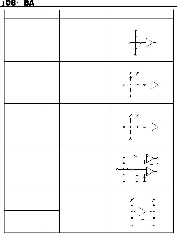
OS |
|
|
|
.com |
L: Active LOW |
L: 0.8 V (max) |
H: Active HIGH |
H: Vrefout − 1 V (min) |
|
et4U |
|
|
|
|
DataSheet4U.com |
|
|
Analog |
|
Overcurrent protection |
Digital filter: 1 µs (typ.) |
|
signal input pin |
Idc |
|
|
Gate protected at 0.5 V or higher |
|
|
(released at carrier cycle) |
Clock signal input pin |
Xin |
Operating range
2 MHz to 8 MHz (crystal oscillation)
Clock signal output pin |
Xout |
TB6556F/FG
Input/Output Internal Circuit
VCC
100 Ω
Vrefout Vrefout
 100 kΩ
2 kΩ
Vrefout Vrefout
 100 kΩ
2 kΩ
VCC 100 Ω
|
Gout |
|
200 kΩ |
Gin |
|
Comparator |
||
|
||
5 pF |
0.5 V |
Vrefout Vrefout
Xin 

 Xout
Xout
360 kΩ
DataShe
DataSheet4U.com
6 |
2005-01-19 |
DataSheet4U.com

www.DataSheet4U.com
TB6556F/FG
Pin Description |
Symbol |
Input/Output Signal |
Input/Output Internal Circuit |
VCC VCCVCC
Reference voltage signal |
Vrefout 5 ± 0.5 V (max 30 mA) |
output pin |
|
|
|
|
|
|
|
|
|
|
|
|
|
|
|
|
|
|
|
|
|
|
|
|
|
|
|
|
|
|
|
|
|
|
|
|
|
|
|
|
|
|
|
|
|
|
|
|
|
|
|
|
|
|
|
|
|
|
|
|
|
|
|
|
|
|
|
|
|
|
|
|
|
|
|
|
|
|
|
|
|
|
|
|
|
|
|
|
|
|
|
|
|
|
|
|
|
|
|
|
|
|
|
|
|
|
|
|
|
|
|
|
|
|
|
|
|
|
|
|
|
|
|
|
|
|
|
|
|
|
|
|
|
|
|
|
|
|
|
|
|
|
|
|
|
|
|
|
|
|
|
|
|
|
|
|
|
|
|
|
|
|
|
|
|
|
|
|
|
|
|
|
|
|
|
|
|
|
|
|
|
|
|
|
|
|
|
|
|
Vrefout |
|
|
|
|
Vrefout |
||||||||||||
|
|
|
|
|
|
|
|
|
|
|
|
|
|
|
|
|
|
|
|
|
|
|
Reverse-rotation-detection |
Digital |
|
|
|
|
|
|
|
|
|
|
|
|
|
|
|
|
|
||||
|
|
|
|
|
|
|
|
|
|
|
|
|
|
|
|
|
||||||
REV |
|
|
|
|
|
|
|
|
|
|
|
|
|
|||||||||
signal output pin |
|
|
|
|
|
|
|
|
|
|
|
|
|
|||||||||
Push-pull output: ± 1 mA (max) |
|
|
|
|
|
|
|
|
|
|
|
|
|
|||||||||
|
100 Ω |
|
|
|
|
|
||||||||||||||||
|
|
|
|
|
|
|
|
|
|
|
|
|
|
|||||||||
|
|
|
|
|
|
|
|
|
|
|
||||||||||||
|
|
|
|
|
|
|
|
|
|
|
|
|
|
|
|
|
|
|
|
|
|
|
|
|
|
|
|
|
|
|
|
|
|
|
|
|
|
|
|
|
|
|
|
|
|
.com |
|
et4U |
DataShe |
|
|
Vrefout |
Vrefout |
DataSheet4U.com
Digital
FG signal output pin FG
Push-pull output: ± 1 mA (max)  100 Ω
100 Ω
|
|
Vrefout |
|
|
|
|
||||||
|
|
|
|
|
|
|||||||
Turn-on signal output pin U |
U |
Analog |
|
|
|
|
|
|
|
|
|
|
Turn-on signal output pin V |
V |
|
|
|
|
|
|
|
|
|
|
|
Push-pull output: ± 2 mA (max) |
|
|
|
|
|
|
||||||
Turn-on signal output pin W |
W |
|
|
|
|
|
||||||
|
|
|||||||||||
|
|
|
|
|
|
|||||||
Turn-on signal output pin X |
X |
|
|
|
|
|
|
100 Ω |
|
|||
Turn-on signal output pin Y |
Y |
L: 0.78 V (max) |
|
|
|
|
|
|
|
|
|
|
|
|
|
|
|
|
|
|
|
|
|||
Turn-on signal output pin Z |
Z |
H: Vrefout − 0.78 V (min) |
|
|
|
|
|
|||||
|
|
|
|
|
|
|
|
|
||||
|
|
|
|
|
|
|
|
|
|
|
|
|
|
|
|
|
|
|
|
|
|
|
|
|
|
DataSheet4U.com
7 |
2005-01-19 |
DataSheet4U.com
 Loading...