

UC2906
UC3906
Sealed Lead-Acid Battery Charger
FEATURES
• Optimum Control for Maximum
Battery Capacity and Life
• Internal State Logic Provides
Three Charge States
• Precision Reference T racks
Battery Requirements Over
Temperature
• Controls Both Voltage and
Current at Charger Output
• System Interface Funct ions
• Typical Standby Supply
Current of only 1.6mA
DESCRIPTION
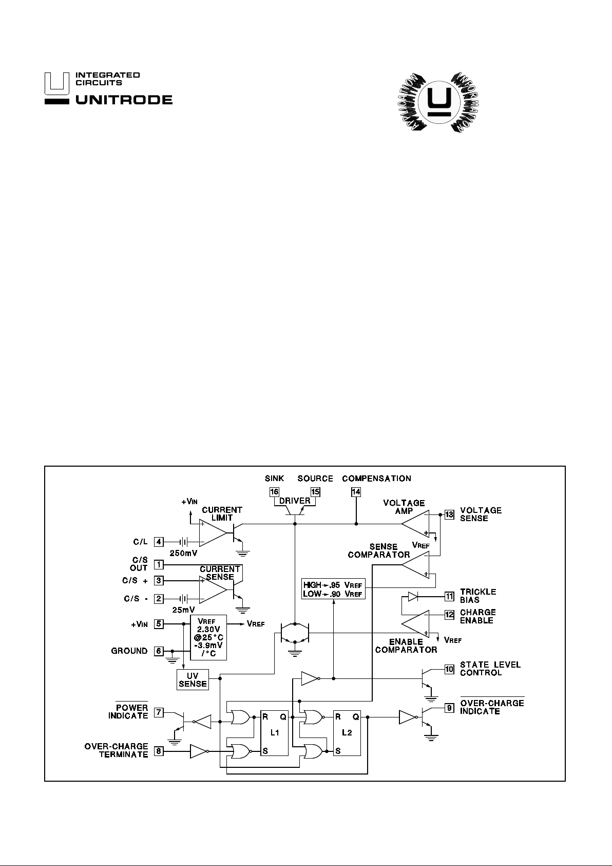
The UC2906 series of batter y charger controllers contains all of the necessary
circuitry to optimally control the charge and hold cycle for s ealed lead-acid batteries. These integrated circuits monitor and control both the output voltage and current of the charger through three separate charge states; a high current
bulk-charge state, a controlled over-charge, and a precision float-charge, or
standby, state.
Optimum charging conditions are maintained over an extended temperature
range with an internal reference that tracks the nominal temperature characteristics of the lead-acid cell. A typical standby supply current requirement of only
1.6mA allows these ICs to predictably monitor ambient temperatures.
Separate voltage loop and current limit amplifiers regulate the output voltage and
current levels in the charger by controlling the onboard driver. The driver will supply up to 25mA of base drive to an external pass device. Voltage and current
sense comparators are used to sense the battery condition and respond with
logic inputs to the charge state logic. A charge enable comparator with a trickle
bias output can be used to implement a low current turn-on mode of the charger,
preventing high curren t charging during abnormal conditions such as a shorted
battery cell.
Other features inclu de a su ppl y unde r-voltage sense circuit with a logic output to
indicate when input power is present. In addition the over-charge state of the
charger can be externa lly monitored and termin ated using the over-charge indicate output and over-charge terminate input.
BLOCK DIAGRA M
SLUS186 - SEPTEMBER 1996
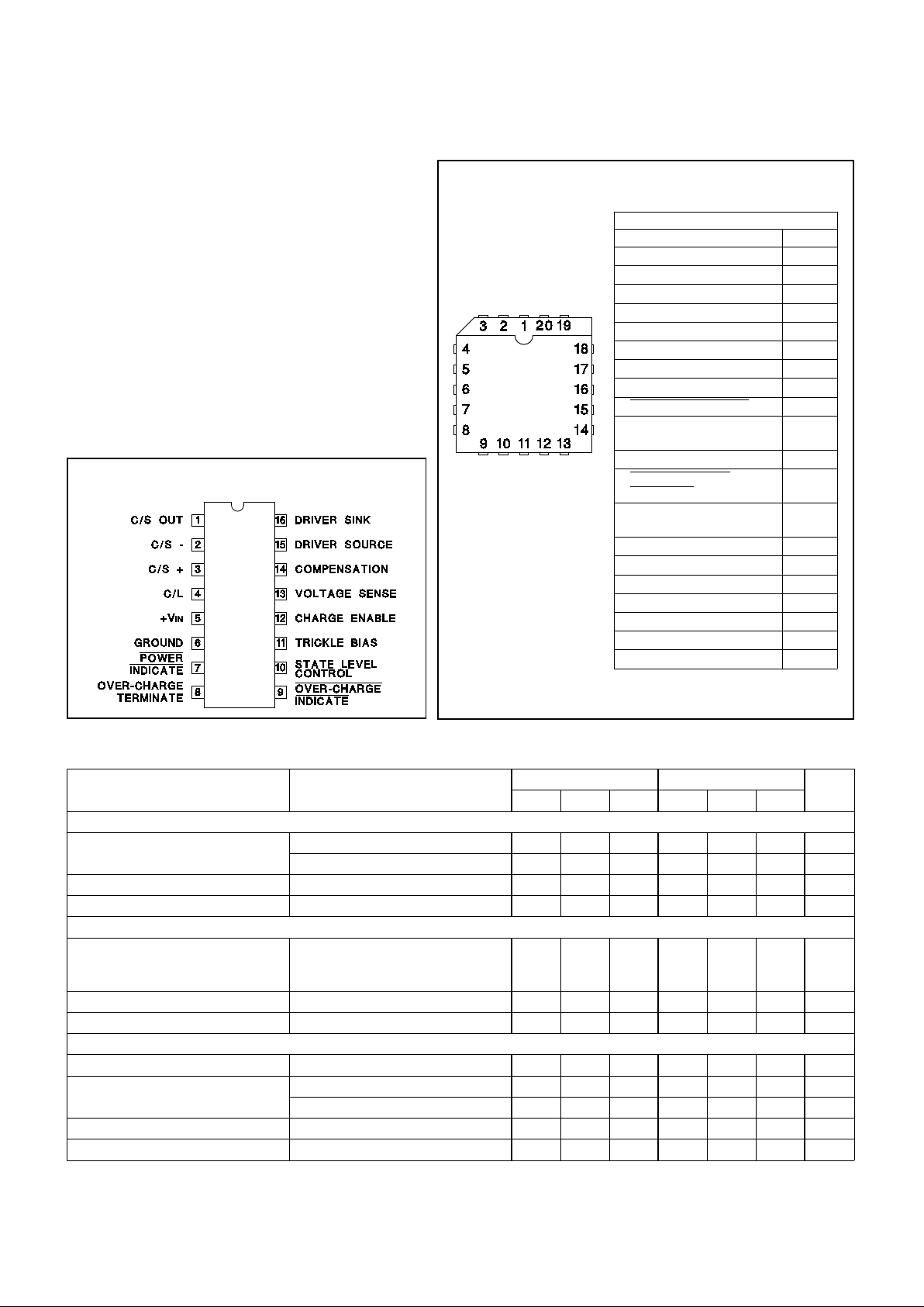
CONNECTION DIAG RAMS
UC2906
UC3906
Supply Voltage (+ VIN). . . . . . . . . . . . . . . . . . . . . . . . . . . 40V
Open Collector Output Voltages. . . . . . . . . . . . . . . . . . . 40V
Amplifier and Comp arato r Input Voltages . . . -0.3V to +40V
Over-Charge Te rm inate I nput Volt age. . . . . . -0.3V to +40V
Current Sense Amplifier Output Cur ren t . . . . . . . . . . 80mA
Other Open Collector Output Currents. . . . . . . . . . . . 20mA
Trickle Bias Voltage Differe nt ial with res pect to V
IN. . . -32V
Trickle Bias Outpu t Current . . . . . . . . . . . . . . . . . . . . -40mA
Driver Current. . . . . . . . . . . . . . . . . . . . . . . . . . . . . . . 80mA
Power Dissipation at T
A = 25°C(Note 2) . . . . . . . . 1000mW
Power Dissipation at T
C = 25°C (Note 2). . . . . . . . 2000mW
Operating Junct ion Te mp era ture . . . . . . . . -55°C to +150°C
Storage Temperature . . . . . . . . . . . . . . . . . -65°C to +150°C
Lead Tempera ture (Solderin g, 10 Seconds) . . . . . . . 300°C
Note 1: Voltage s are reference d to ground (Pin 6) . Current s
are positive into, negat ive out of, the specif ied te rminals.
Note 2: Consult Packag in g sect ion of Dat abo ok f or ther ma l
limitations and considerat ions of packages .
DIL-16, SOIC- 16 (T O P VIEW)
J or N Package, DW Package
PACKAGE PIN FUNCTION
FUNCTION PIN
N/C 1
C/S OUT 2
C/S- 3
C/S+ 4
C/L 5
N/C 6
+VIN 7
GROUND 8
POWER INDICATE 9
OVER CHARGE
TERMINATE
10
N/C 11
OVER CHARGE
INDICATE
12
STATE LEVEL
CONTROL
13
TRICKLE BIAS 14
CHARGE ENABLE 15
N/C 16
VOLTAGE SENSE 17
COMPENSATION 18
DRIVER SOURCE 19
DRIVER SINK 20
PLCC-20, LCC-20
(TOP VIEW)
Q, L Packages
ABSOLUTE MAXI MUM RATING S (Note 1)
PARAMETER TEST CONDITIONS UC2906 UC3906 UNITS
MIN TYP MAX MIN TYP MAX
Input Supply
Supply Current +V
IN = 10V 1.6 2.5 1.6 2.5 mA
+V
IN = 40V 1.8 2.7 1.8 2.7 mA
Supply Under-Voltage Threshold +V
IN = Low to High 4.2 4.5 4.8 4.2 4.5 4.8 V
Supply Under-Voltage Hysteresis 0.20 0.30 0.20 0.30 V
Internal Reference (V
REF)
Voltage Level (Note 3) Measured as Regulating Level at
Pin 13 w/ Driver Current = 1mA,
T
J = 25°C
2.275 2.3 2.325 2.270 2.3 2.330 V
Line Regulation +V
IN = 5 to 40V 38 38mV
Temperature Coeff icient -3.9 -3.9 mV/°C
Voltage A m pl if ier
Input Bias Current Total Input Bias at Regulating Level -0.5 -0.2 -0.5 -0.2 µA
Maximum Output Current Source -45 -30 -15 -45 -30 -15 µA
Sink 30 60 90 30 60 90 µA
Open Loop Gain Driver current = 1mA 50 65 50 65 dB
Output Voltage Swing Volts above GND or below +V
IN 0.2 0.2 V
Unless otherwise st ated, these specif icat ions apply fo r T
A = -40°C to +70°C for the
UC2906 and 0°C to +70°C for the UC3906, +V
IN = 10V, TA = TJ.
ELECTRICAL CHARACTERISTICS:
Note 3. The referenc e volt age will change as a function of power dissipat ion on the die according t o the tem per ature coef ficie nt of
the reference and the t her mal resist anc e, junct ion-t o-am bient .
2
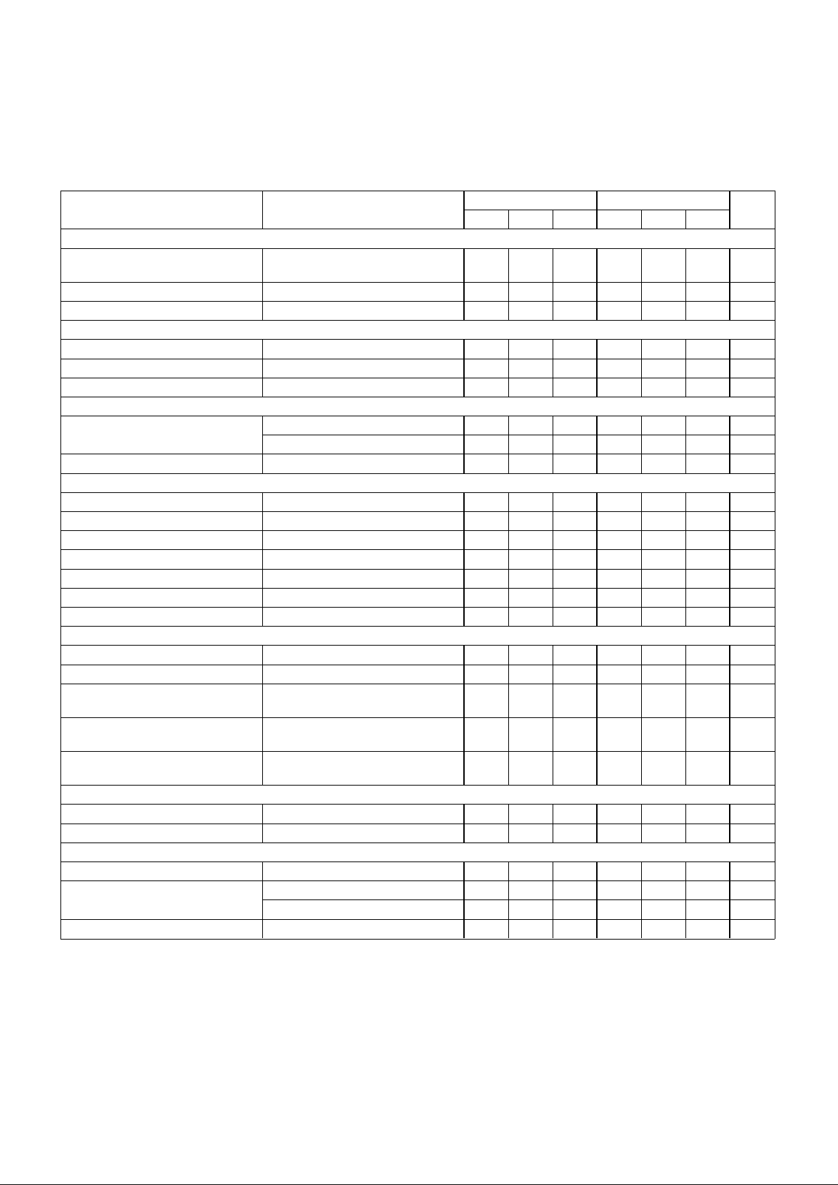
PARAMETER TEST CONDITIONS UC2906 UC3906 UNITS
MIN TYP MAX MIN TYP MAX
Driver
Minimum Supply to Source
Different ial
Pin 16 = +V
IN, IO = 10mA 2.0 2.2 2.0 2.2 V
Maximum Output Current Pin 16 to Pin 15 = 2V 25 40 25 40 mA
Saturation Voltage 0.2 0.45 0.2 0.45 V
Current Limit Amplifier
Input Bias Current 0.2 1.0 0.2 1.0 µA
Threshold Voltage Of f set below + V
IN 225 250 275 225 250 275 mV
Threshold Supply Sen sitivit y +V
IN = 5 to 40V 0.03 0.25 0.03 0.25 %/V
Voltage Sense Compar ator
Threshold Voltage As a func tion of V
REF, L1 = RESET 0.945 0.95 0.955 0.945 0.95 0.955 V/V
As a function of V
REF, L1 = SET 0.895 0.90 0.905 0.895 0.90 0.905 V/V
Input Bias Current Total Input Bias at Thresholds -0.5 -0.2 -0.5 -0.2 µA
Current Sense Comparato r
Input Bias Current 0.1 0.5 0.1 0.5 µA
Input Offs et Cu rr ent 0.01 0.2 0.01 0.2 µA
Input Offset Voltag e Referenced t o Pin 2, I
OUT = 1mA 202530202530mV
Offset Supply Sensitivity +V
IN = 5 to 40V 0.05 0.35 0.05 0.35 %/V
Offset Common Mode Sensitivity CM V = 2V to +V
IN 0.05 0.35 0.05 0.35 %/V
Maximum Output Current V
OUT = 2V 25 40 25 40 mA
Output Saturat io n Volta ge I
OUT = 10mA 0.2 0.45 0.2 0.45 V
Enable Comparator
Threshold Voltage As a func tion of V
REF 0.99 1.0 1.01 0.9 9 1.0 1.01 V/V
Input Bias Current -0.5 -0.2 -0.5 -0.2 µA
Trickle Bias Maximu m Outpu t
Current
V
OUT = +VIN − 3V 25 40 25 40 mA
Trickle Bias Maximu m Outpu t
Voltage
Volts below +V
IN, IOUT = 10mA 2.0 2.6 2.0 2.6 V
Trickle Bias Reverse Hold-Of f
Voltage
+V
IN = 0V, IOUT = -10µA 6.3 7.0 6.3 7.0 V
Over-Charg e Termi na te Inpu t
Threshold Voltage 0.7 1.0 1.3 0.7 1.0 1.3 V
Internal Pull-Up Current At Threshold 10 10 µA
Open Collector Outputs (Pins 7, 9, and 10)
Maximum Output Current V
OUT = 2V 2.5 5 2.5 5 mA
Saturation Voltage I
OUT = 1.6mA 0.25 0.45 0.25 0.45 V
I
OUT = 50µ A 0 .0 3 0.05 0.03 0.05 V
Leakage Curr ent V
OUT = 40V 13 13µA
ELECTRICAL CHARACTERISTICS:
Unless otherwise st ated, these specif icat ions apply fo r TA = -40°C to +70°C for the
UC2906 and 0°C to +70°C for the UC3906, +V
IN = 10V, TA = TJ.
UC2906
UC3906
3

Dual Level Float Charg er Ope ration s
The UC2906 is shown configured as a dual level float
charger in Fig ure 1. All high currents are handled by the
external PNP pass transistor with the driver supplying
base drive to this device. This scheme uses the TRICKLE
BIAS output and the charge enable comparator to give
the charger a low current turn on mode. The ou tput current of the charger is limited to a low-level until the battery
reaches a specified voltage, preventing a high current
charging if a battery cell is shorted. Figure 2 shows the
state diagram o f the charger. Upon turn on the UV sense
circuitry puts the charger in state 1, the high rate bulkcharge state. In this state, once the enable threshold has
been exceeded, the charger will supply a peak current
that is determined by the 250mV offset in the C/L amplifier and the sensing resistor R
S.
To guarantee full re-charge of the battery, the charger’s
voltage loop has an elevated regulating level, V
OC, during
state 1 and state 2. When the battery voltage reaches
95% of VOC, the charger enters the over-charge state,
state 2. The charge r stays in this state until the OVERCHARGE TERMINATE pin goes high. In Figure 1, the
charger use s the curren t sense amplifier to generate this
signal by sensing when the charge current has tapered to
a specified level, I
OCT. Alternatively the over-charge could
have been controlled by an external source, such as a
timer, by using the
OVER-CHARGE INDICATE signal at
Pin 9. If a load is applied to the battery and begins to discharge it, the charger will contribute its full output to the
load. If the battery drops 10% below the float level, the
charger will reset itself to state 1. When the load is removed a full charge cycle will follow. A graphical representation of a charge, and discharge, cycle of the dual
lever float charger is shown in Figure 3.
UC2906
UC3906
Figure 1. T he UC2906 in a Dual Level Float Charger
OPERATION AND APPLICATI ON INFO RMATI ON
Internal Reference Temperature Characteristic and
T o leran ce
4

Design procedure
1.) Pick divider current, ID. Recommended value is
50µA to 1 0 0µ A.
2.)
R
C
= 2.3
V
⁄
I
D
3.)
R
A
+
R
B
=
R
SUM
= (
V
F
− 2.3V )⁄
I
D
4.)
R
D
= 2.3
VR
SUM
⁄ (
V
OC
−
V
F
)
5.)
R
A
= (
R
SUM
+
R
X
) (1 −2.3
V
⁄
V
T
)
where:
R
X
=
RCR
D
⁄
(
R
C
+
R
D
)
6.)
R
B
=
R
SUM
−
R
A
7.)
R
S
= 0.25
V
⁄
I
MAX
8.)
R
T
= (
V
IN
−
V
T
− 2.5V )
⁄
I
T
Note:V
12 = 0.95
V
OC
V
31 = 0.90
V
F
I
OCT
=
I
MAX
10
For further design and applicat ion inf ormation se e
UICC Appl ication Not e U-10 4
Explanati on: Dual Level Float Charger
A. Input power turns on, batter y charge s at trickle cur ren t rat e.
B. Battery volt age reaches V T enab ling the driver and turning
off the trickle bias output , battery cha rges at l
MAX rate.
C. Transition voltage V
12 is reached and the charger indicates
that it is now in the over-charge state, state 2.
D. Ba tter y voltage appr oach es the ove r-char ge leve l V
OC and
the charge cur re nt begins t o taper.
E. Charg e curren t ta pe rs to l
OCT. The current sense amplifier
output, in this case tied to the OC TERMINATE input,
goes high. The charger changes to the float state and
holds the battery voltage at V
F.
F. Here a load (>l
MAX) begins to discharg e the batt ery.
G. The load discharges the ba ttery suc h that the batte ry
voltage falls below V
31. The charger is now in stat e 1,
again.
UC2906
UC3906
OPERATION AND APPLICATI ON INFO RMATI ON (co ntinu ed)
Figure 2. State Diagram and Design Equation s for the Dual Level Flo at Charg er
Figure 3. Typical Charge Cycle: UC2906 Dual Level Flo at Charger
5

Compensa ted Refere nce Match es Battery Req uireme nts
When the charger is in the float state, the battery will be
maintained at a precise float voltage, V
F. The accuracy of
this float state will maximize the standby life of the battery
while the bulk-charge and over-charge states guarantee
rapid and full re-charge. All of the voltage thresholds on
the UC2906 are deri ved from the internal referen ce. This
reference has a temperature coefficient that tracks the
temperature characteristic of the optimum-charge and
hold levels for sealed lead-acid cells. This further guarantees that proper charging occurs, even at temperature extremes.
Dual Step Current Charg er Ope ration
Figures 4, 5 and 6 i ll ustrate the UC2906’s use in a different charging scheme. The dual step current charger is
useful when a large string of series cells must be
charged. The holding-charge state maintains a slightly
elevated voltage across the batteries with the holding current, 1
H. This will tend to guarantee equal charge distribu-
tion between the cell s. The bulk-charge state is similar to
that of the fl oat charger with the exception that when V
12
is reached, no over-charge state occurs since Pin 8 is tied
high at all times. The current sense amplifier is used to
regulate the holding current. In some applications a series
resistor, or external buffering transistor, may be required
at the current sense output to prevent excessive power
dissipation on the UC2906.
A PNP Pass Device Reduces Minimum Input to Output Differenti al
The configuration o f the driver on the UC2906 a llows a
good bit of flexibilit y when interfacing to an external pass
transistor. The two chargers shown in Figures 1 and 4
both use PNP pass devices, although an NPN device
driven from the source output of the UC2906 driver can
also be used. In situati ons where the charger must operate with low input to output differentials the PNP pass device should be configured as shown in Figure 4. The PNP
can be operated in a saturated mode with only the series
diode and sense resistor a ddi ng to the minimum differential. The series diode, D1, in many applications, can be
eliminated. This diode prevents any discharging of the
battery, except through the sensing divider, when the
charger is attached to the battery with no input supply
voltage. If discharging under this condition must be kept
to an absolute minimum, the sense divider can be referenced to the
POWER INDICATE pin, Pin 7, instead of
ground. In thi s manne r the open col lector off state of Pin
7 will prevent the divider resistors from discharging the
battery when the input supply is removed.
UC2906
UC3906
Figure 4. T he UC2906 in a Dual Step Current Char ger
OPERATION AND APPLICATI ON INFO RMATI ON (continued)
6

A. Input power turns on, bat t er y charges at a rate of IH + IMAX.
B. Battery voltage reaches V12 and th e voltage loop switch es
to the lower level V
F. The battery is now fed with the holding
current I
H.
C. An external load starts to discharge the battery.
D. When V
F is reached the charger will supply the full
current I
MAX + IH.
E. The discharge cont in ues an d the bat t ery volta ge reache s
V21 causing the charg er to switch bac k to state 1.
OPERATION AND APPLICATI ON INFO RMATI ON (continued)
UC2906
UC3906
Explanati on: Dual Step Cur re nt Cha rger
Figure 5. State Diagram and Design Equation s for the Dual Step Cur rent Charge r
Figure 6. Typical Charge Cycle: UC2906 D ual Step Current Charger
UNITRODE INTEGRATED CIRCUITS
7 CONTINENTAL BLVD. • MERRIMACK, NH 03054
TEL. 603-424-2410 • FAX 603-424-3460
7

IMPORTANT NOTICE
T exas Instruments and its subsidiaries (TI) reserve the right to make changes to their products or to discontinue
any product or service without notice, and advise customers to obtain the latest version of relevant information
to verify, before placing orders, that information being relied on is current and complete. All products are sold
subject to the terms and conditions of sale supplied at the time of order acknowledgement, including those
pertaining to warranty, patent infringement, and limitation of liability.
TI warrants performance of its semiconductor products to the specifications applicable at the time of sale in
accordance with TI’s standard warranty. Testing and other quality control techniques are utilized to the extent
TI deems necessary to support this warranty. Specific testing of all parameters of each device is not necessarily
performed, except those mandated by government requirements.
CERT AIN APPLICATIONS USING SEMICONDUCTOR PRODUCTS MAY INVOLVE POTENTIAL RISKS OF
DEATH, PERSONAL INJURY, OR SEVERE PROPERTY OR ENVIRONMENTAL DAMAGE (“CRITICAL
APPLICATIONS”). TI SEMICONDUCTOR PRODUCTS ARE NOT DESIGNED, AUTHORIZED, OR
WARRANTED TO BE SUITABLE FOR USE IN LIFE-SUPPORT DEVICES OR SYSTEMS OR OTHER
CRITICAL APPLICATIONS. INCLUSION OF TI PRODUCTS IN SUCH APPLICA TIONS IS UNDERSTOOD T O
BE FULLY AT THE CUSTOMER’S RISK.
In order to minimize risks associated with the customer’s applications, adequate design and operating
safeguards must be provided by the customer to minimize inherent or procedural hazards.
TI assumes no liability for applications assistance or customer product design. TI does not warrant or represent
that any license, either express or implied, is granted under any patent right, copyright, mask work right, or other
intellectual property right of TI covering or relating to any combination, machine, or process in which such
semiconductor products or services might be or are used. TI’s publication of information regarding any third
party’s products or services does not constitute TI’s approval, warranty or endorsement thereof.
Copyright 1999, Texas Instruments Incorporated
 Loading...