

Page 1
Ajinder Singh, Natarajan Viswanathan
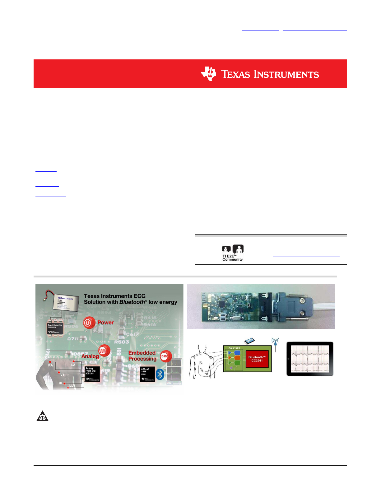
TI Designs
Wireless Heart Rate Monitor Reference Design
TI Designs Design Features
TI Designs provide the foundation that you need The Wireless Heart Rate Monitor with Bluetooth® lowincluding methodology, testing and design files to energy (BLE) is a reference design for customers to
quickly evaluate and customize and system. TI develop end-products for battery-powered 3-channel
Designs help you accelerate your time to market. health and fitness electrocardiogram (ECG)
Design Resources
TIDA-00096
ADS1293 Product Folder
CC2541 Product Folder
TPS61220 Product Folder
CC Debugger
Tool Folder Containing Design Files
Small Programmer and Debugger for
Low-Power RF System-on-Chips
applications.
• Supports 5-Lead ECG applications
• Easily monitor heart rate data through an iOS
Mobile Application
• Powered by a Lithium-ion battery
• EMI filters integrated in the ADS1293 device reject
Interference from outside RF sources
• Open-source Firmware and iOS application
enables quick time-to-market for customers
Featured Applications
• Health and Fitness
ASK Our Analog Experts
WebBench™ Calculator Tools
An IMPORTANT NOTICE at the end of this TI reference design addresses authorized use, intellectual property matters and other
important disclaimers and information.
WebBench is a trademark of Texas Instruments.
All other trademarks are the property of their respective owners.
TIDU195A–January 2014–Revised July 2014 Wireless Heart Rate Monitor Reference Design
Submit Documentation Feedback
1
Copyright © 2014, Texas Instruments Incorporated
Page 2

System Description
1 System Description
The heart of the Wireless Heart Rate Monitor is the ADS1293 device (analog front-end) and the CC2541
device (Bluetooth-low energy SOC) as shown in Figure 1. The ADS1293 device is a highly integrated lowpower analog front-end (AFE) that features three high-resolution ECG channels. The CC2541 system-onchip (SoC) adds a BLE wireless feature to the platform. BLE enables seamless connectivity to an iPhone®
or an iPad® through a configurable iOS application that allows an end-user to remotely monitor the heartrate data of a patient.
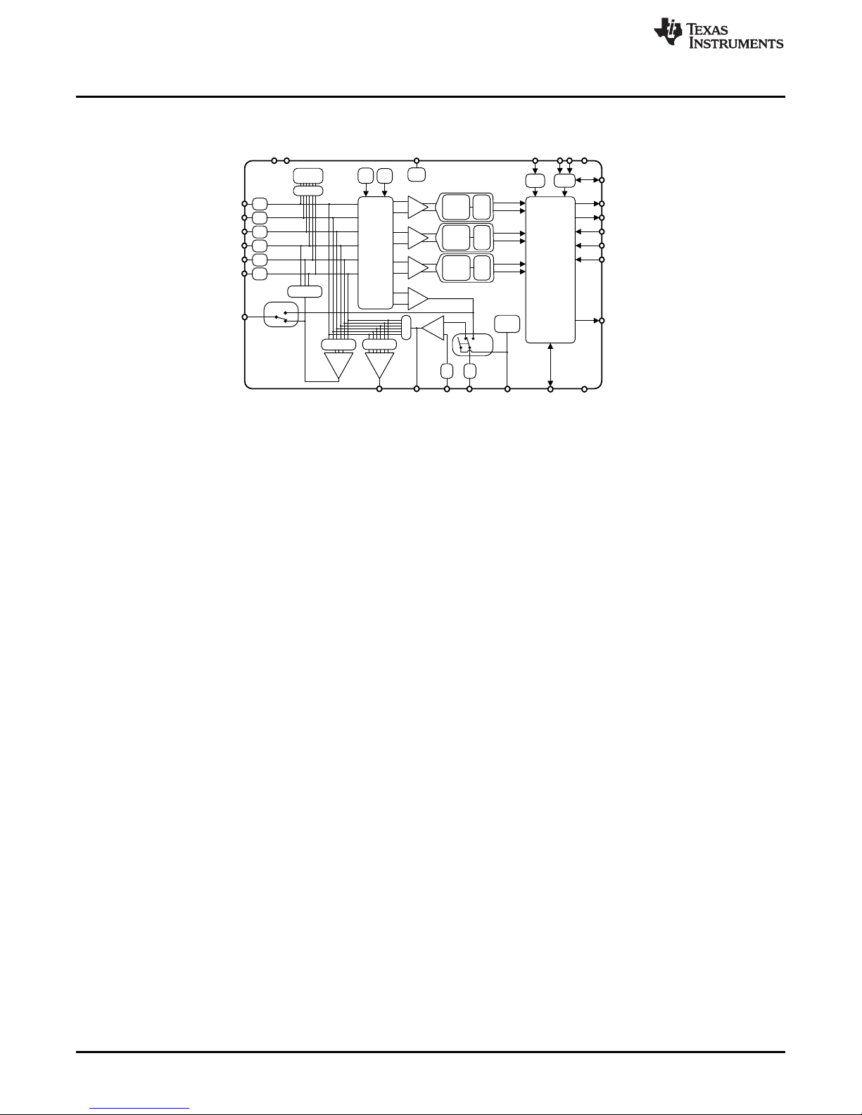
1.1 ADS1293
The ADS1293 incorporates all features commonly required in portable, low-power medical, sports, and
fitness electrocardiogram (ECG) applications. With high levels of integration and exceptional performance,
the ADS1293 enables the creation of scalable medical instrumentation systems at significantly reduced
size, power, and overall cost.
The ADS1293 features three high-resolution channels capable of operating up to 25.6ksps. Each channel
can be independently programmed for a specific sample rate and bandwidth allowing users to optimize the
configuration for performance and power. All input pins incorporate an EMI filter and can be routed to any
channel via a flexible routing switch. Flexible routing also allows independent lead-off detection, right leg
drive, and Wilson/Goldberger reference terminal generation without the need to reconnect leads
externally. A fourth channel allows external analog pace detection for applications that do not utilize digital
pace detection. For the ADS1293 block diagram, see Figure 2.
The ADS1293 incorporates a self-diagnostics alarm system to detect when the system is out of the
operating conditions range. Such events are reported to error flags. The overall status of the error flags is
available as a signal on a dedicated ALARMB pin. The device is packaged in a 5-mm × 5-mm × 0,8-mm,
28-pin LLP. Operating temperature ranges from –20°C to 85°C.
www.ti.com
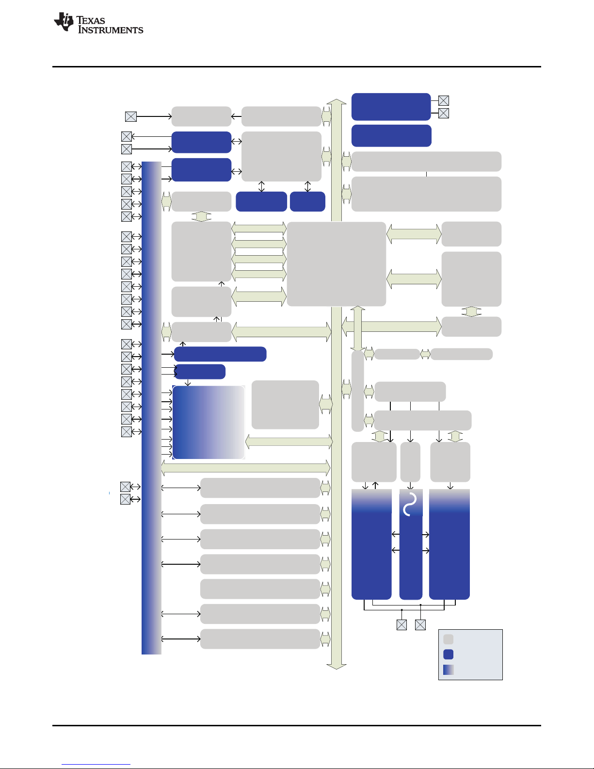
1.2 CC2541
The CC2541 is a power-optimized true system-on-chip (SoC) solution for both Bluetooth low energy and
proprietary 2.4-GHz applications. It enables robust network nodes to be built with low total bill-of-material
costs. The CC2541 combines the excellent performance of a leading RF transceiver with an industrystandard enhanced 8051 MCU, in-system programmable flash memory, 8-KB RAM, and many other
powerful supporting features and peripherals. The CC2541 is highly suited for systems where ultralow
power consumption is required. This is specified by various operating modes. Short transition times
between operating modes further enable low power consumption.
The CC2541 is pin-compatible with the CC2540 in the 6-mm × 6-mm QFN40 package, if the USB is not
used on the CC2540 and the I2C/extra I/O is not used on the CC2541. Compared to the CC2540, the
CC2541 provides lower RF current consumption. The CC2541 does not have the USB interface of the
CC2540, and provides lower maximum output power in TX mode. The CC2541 also adds a HW I2C
interface.
The CC2541 is pin-compatible with the CC2533 RF4CE-optimized IEEE 802.15.4 SoC. The CC2541
comes in two different versions: CC2541F128/F256, with 128 KB and 256 KB of flash memory,
respectively. For the CC2541 block diagram, see Figure 3.
1.3 TPS61220
The TPS6122x family devices provide a power-supply solution for products powered by either a singlecell, two-cell, or three-cell alkaline, NiCd or NiMH, or one-cell Li-Ion or Li-polymer battery. Possible output
currents depend on the input-to-output voltage ratio. The boost converter is based on a hysteretic
controller topology using synchronous rectification to obtain maximum efficiency at minimal quiescent
currents. The output voltage of the adjustable version can be programmed by an external resistor divider,
or is set internally to a fixed output voltage. The converter can be switched off by a featured enable pin.
While being switched off, battery drain is minimized. The device is offered in a 6-pin SC-70 package
(DCK) measuring 2 mm × 2 mm to enable small circuit layout size. For the TPS61220 block diagram, see
Figure 4.
2
Wireless Heart Rate Monitor Reference Design TIDU195A–January 2014–Revised July 2014
Copyright © 2014, Texas Instruments Incorporated
Submit Documentation Feedback
Page 3
ADS1293
Analog Front End
CC2541
ADC + uP + BLE
TPS61220
Boost Converter
Battery
www.ti.com
2 Block Diagram
Figure 1. Temperature Transmitter System Block Diagram
2.1 Highlighted Products
The Wireless Heart Rate Monitor Reference Design features the following devices:
• ADS1293
– ADS1293 Low Power, 3-Channel, 24-Bit Analog Front End for Biopotential Measurements
• CC2541
– 2.4-GHz Bluetooth™ low energy and Proprietary System-on-Chip
• TPS61220
– TPS6122x Low Input Voltage, 0.7V Boost Converter With 5.5μA Quiescent Current
For more information on each of these devices, see the respective product folders at www.TI.com.
Block Diagram
TIDU195A–January 2014–Revised July 2014 Wireless Heart Rate Monitor Reference Design
Submit Documentation Feedback
Copyright © 2014, Texas Instruments Incorporated
3
Page 4
CH1-ECG
CH2-ECG
CH3-ECG
Lead off
detect
-
+
EMI
filter
CSB
SCLK
SDI
SDO
OSC
IN1
Flexible
Routing
Switch
Test
Ref
XTAL1
-
+
VSS
VDD
VDDIO
CVREF
RLDINV
RLDIN
EMI
filter
IN2
EMI
filter
IN3
EMI
filter
IN4
EMI
filter
IN5
EMI
filter
IN6
Batt.
Mon
CMOUT
XTAL2
POR
RSTB
DRDYB
RLDREF
CLK
ALARMB
DIGITAL
CONTROL AND
POWER
MANAGEMENT
Wilson
ref.
CM
Detect
SYNCB
VSSIO
Digital
Filter
Σ∆
Modulator
Digital
Filter
Σ∆
Modulator
-
+
-
+
InA
InA
InA
WCT
-
+
CH4- Analog Pace
WILSON_EN
CMDET_EN
SELRLD
REF
EMI
filter
EMI
filter
LOD_EN
CH1-Pace
CH2-Pace
CH3-Pace
Digital
Filter
Σ∆
Modulator
REF for
CM & RLD
RLD
Amp.
PACE2
RLDIN
PACE2WCT
WILSON_CN
CH1
CH2
CH3
CH4 InA
Block Diagram
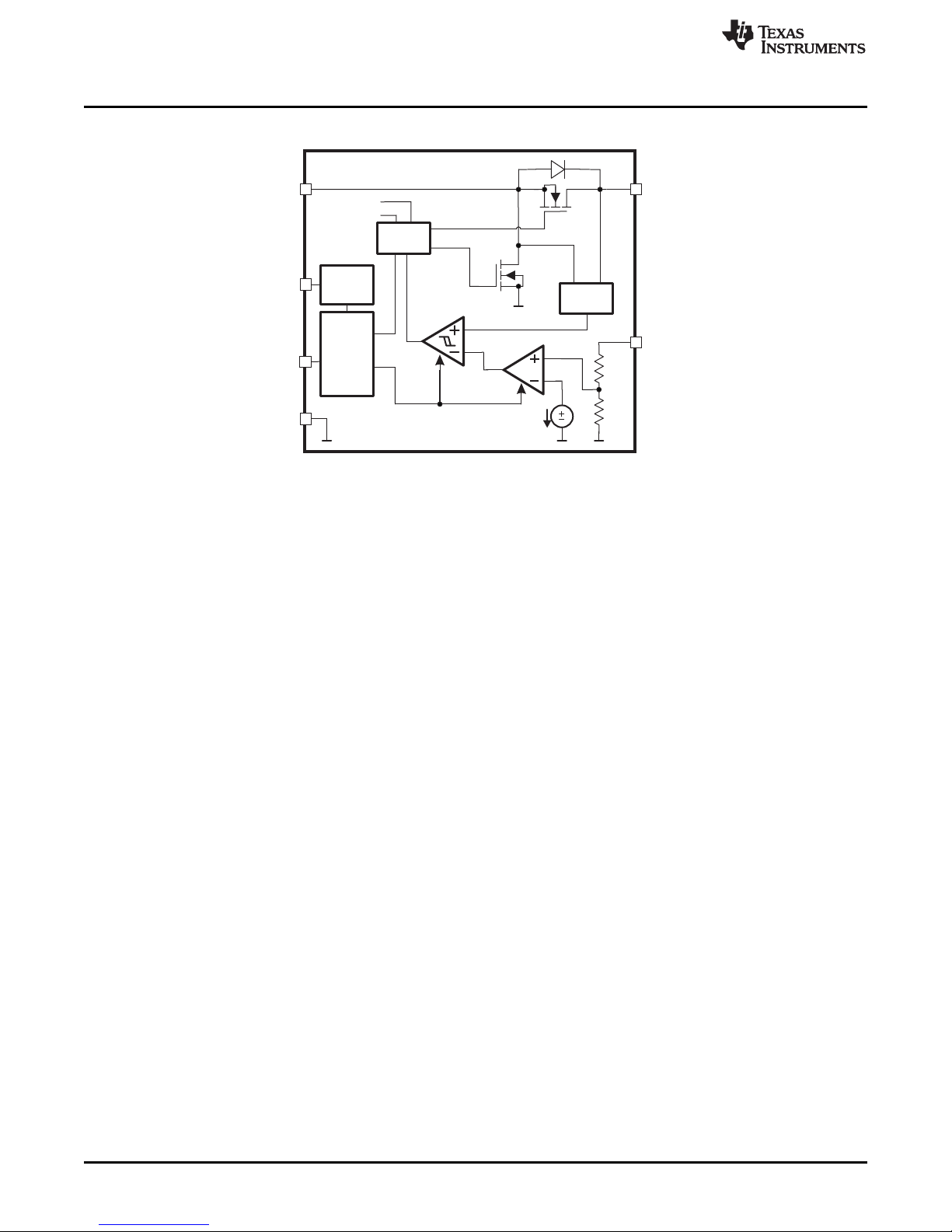
2.1.1 ADS1293
• Low current consumption:
– Duty-Cycle mode: 120 μA
– Normal mode: 415 μA
• Wide supply range: 2.3 V to 5.5 V
• Programmable gain: 1 V/V to 128 V/V
• Programmable data rates: Up to 2 kSPS
• 50-Hz and 60-Hz rejection at 20 SPS
• Low-noise PGA: 90 nV
• Dual matched programmable current sources: 10 μA to 1500 μA
• Internal temperature sensor: 0.5°C Error (max)
• Low-drift internal reference
• Low-drift internal oscillator
• Two differential or four single-ended inputs
• SPI™-compatible interface
• 3,5 mm × 3,5 mm × 0,9 mm QFN package
Figure 2. ADS1293 Block Diagram
at 20 SPS
RMS
www.ti.com
Wireless Heart Rate Monitor Reference Design TIDU195A–January 2014–Revised July 2014
4
Copyright © 2014, Texas Instruments Incorporated
Submit Documentation Feedback
Page 5
SFR bus SFR bus
MEMORY
ARBITRATOR
8051 CPU
CORE
DMA
FLASH
SRAM
FLASH CTRL
DEBUG
INTERFACE
RESET
RESET_N
P2_4
P2_3
P2_2
P2_1
P2_0
P1_4
P1_3
P1_2
P1_1
P1_0
P1_7
P1_6
P1_5
P0_4
P0_3
P0_2
P0_1
P0_0
P0_7
P0_6
P0_5
32.768 kHz
CRYSTAL OSC
32 MHz
CRYSTAL OSC
HIGH SPEED
RC-OSC
32 kHz
RC-OSC
CLOCK MUX &
CALIBRATION
RAM
USART 0
USART 1
TIMER 1 (16-bit)
TIMER 3 (8-bit)
TIMER 2
(BLE LL TIMER)
TIMER 4 (8-bit)
AES
ENCRYPTION
&
DECRYPTION
WATCHDOG TIMER
IRQ
CTRL
FLASH
UNIFIED
RF_P RF_N
SYNTH
MODULATOR
POWER ON RESET
BROWN OUT
RADIO
REGISTERS
POWER MGT. CONTROLLER
SLEEP TIMER
PDATA
XRAM
IRAM
SFR
XOSC_Q2
XOSC_Q1
DS ADC
AUDIO / DC
DIGITAL
ANALOG
MIXED
VDD (2.0 - 3.6 V)
DCOUPL
ON-CHIP VOLTAGE
REGULATOR
Link Layer Engine
FREQUENCY
SYNTHESIZER
I2C
DEMODULATOR
RECEIVE TRANSMIT
OP-AMP
ANALOG COMPARATOR
I/O CONTROLLER
1 KB SRAM
Radio Arbiter
FIFOCTRL
SDA
SCL
www.ti.com
2.1.2 CC2541
Block Diagram
TIDU195A–January 2014–Revised July 2014 Wireless Heart Rate Monitor Reference Design
Submit Documentation Feedback
Figure 3. CC2541 Block Diagram
Copyright © 2014, Texas Instruments Incorporated
5
Page 6

Block Diagram
• RF
– 2.4-GHz Bluetooth low energy Compliant and Proprietary RF System-on-Chip
– Supports 250-kbps, 500-kbps, 1-Mbps, 2-Mbps Data Rates
– Excellent link budget, enabling long-range applications without external front end
– Programmable output power up to 0 dBm
– Excellent receiver sensitivity (–94 dBm at 1 Mbps), selectivity, and blocking performance
– Suitable for systems targeting compliance with worldwide radio frequency regulations: ETSI EN 300
• Layout
– Few external components
– Reference design provided
– 6-mm × 6-mm QFN-40 package
– Pin-compatible with CC2540 (when not using USB or I2C)
• Low Power
– Active-mode RX down to: 17.9 mA
– Active-mode TX (0 dBm): 18.2 mA
– Power mode 1 (4-µs wake-up): 270 µA
– Power mode 2 (sleep timer on): 1 µA
– Power mode 3 (external interrupts): 0.5 µA
– Wide Supply-voltage range (2 V–3.6 V)
• TPS62730 Compatible low power in active mode
– RX down to: 14.7 mA (3-V supply)
– TX (0 dBm): 14.3 mA (3-V supply)
• Microcontroller
– High-performance and low-power 8051 microcontroller core with code Prefetch
– In-system-programmable flash, 128- or 256-KB
– 8-KB RAM with retention in all power modes
– Hardware-debug support
– Extensive baseband automation, including auto-acknowledgment and address decoding
– Retention of all relevant registers in all power modes
• Peripherals
– Powerful five-channel DMA
– General-purpose timers (one 16-Bit, two 8-Bit)
– IR generation circuitry
– 32-kHz sleep timer with capture
– Accurate digital RSSI support
– Battery monitor and temperature sensor
– 12-Bit ADC with eight channels and configurable resolution
– AES security coprocessor
– Two powerful USARTs with support for several serial protocols
– 23 general-purpose I/O Pins (21 × 4 mA, 2 × 20 mA)
– I2C interface
– Two I/O pins have LED Driving capabilities
– Watchdog timer
– Integrated high-performance comparator
• Development Tools
www.ti.com
328 and EN 300 440 Class 2 (Europe), FCC CFR47 Part 15 (US), and ARIB STD-T66 (Japan)
6
Wireless Heart Rate Monitor Reference Design TIDU195A–January 2014–Revised July 2014
Copyright © 2014, Texas Instruments Incorporated
Submit Documentation Feedback
Page 7

www.ti.com
• Software Features
Block Diagram
– CC2541 evaluation module kit (CC2541EMK)
– CC2541 mini development kit (CC2541DK-MINI)
– SmartRF™ software
– IAR embedded Workbench™ available
– Bluetooth v4.0 compliant protocol stack for single-mode BLE solution
• Complete power-optimized stack, including controller and host
• GAP – central, peripheral, observer, or broadcaster (including combination roles)
• ATT / GATT – client and server
• SMP – AES-128 encryption and decryption
• L2CAP
• Sample applications and profiles
• Generic applications for GAP central and peripheral roles
• Proximity, accelerometer, simple keys, and battery GATT services
• More applications supported in BLE Software Stack
• Multiple configuration options
• Single-chip configuration, allowing applications to run on CC2541
• Network processor interface for applications running on an external microcontroller
• BTool – Windows PC application for evaluation, development, and test
TIDU195A–January 2014–Revised July 2014 Wireless Heart Rate Monitor Reference Design
Submit Documentation Feedback
7
Copyright © 2014, Texas Instruments Incorporated
Page 8
Current
Sensor
Gate
Driver
Device
Control
GND
EN
FB
VOUT
L
VREF
VIN
Device
Control
StartUp
VIN
VOUT
Block Diagram
2.1.3 TPS61220
• Up to 95% efficiency at typical operating conditions
• 5.5 μA quiescent current
• Startup into load at 0.7-V input voltage
• Operating input voltage from 0.7 V to 5.5 V
• Pass-through function during shutdown
• Minimum switching current 200 mA
• Protections:
– Output overvoltage
– Overtemperature
– Input undervoltage lockout
• Adjustable output voltage from 1.8 V to 6 V
• Fixed output voltage versions
• Small 6-pin SC-70 package
www.ti.com
Figure 4. TPS61220 Block Diagram
8
Wireless Heart Rate Monitor Reference Design TIDU195A–January 2014–Revised July 2014
Copyright © 2014, Texas Instruments Incorporated
Submit Documentation Feedback
Page 9
V1
-
+
RLDINV
CMOUT
RLDOUT
DIGITAL
CONTROL AND
POWER
MANAGEMENT
Wilson
ref.
Digital
Filter
Σ∆
Modulator
Digital
Filter
Σ∆
Modulator
Digital
Filter
Σ∆
Modulator
-
+
-
+
InA
InA
InA
WCT
-
+
RA LA
LL
RL
IN1
IN2
IN3
IN4
IN5
IN6
R
1
R
2
C
1
I
II
V
SELRLD
WILSON_EN
CM
detect
CMDET_EN
-
+
RLD
Amp.
VSS
VDD
VDDIO
XTAL1
XTAL2
CVREF
5V
InA
CH1
CH2
CSB
SCLK
SDI
SDO
DRDYB
ALARMB
RLDIN
RLDREF
CH3
5V 5V
0.1 F
1
F
4.096
MHz
0.1 F
3.3V
0.1 F
22 pF 22 pF
CLK
VSSIO
SYNCB
1 MΩ
3.3V
REF for
CM & RLD
1 MΩ
RSTB
3.3V
www.ti.com
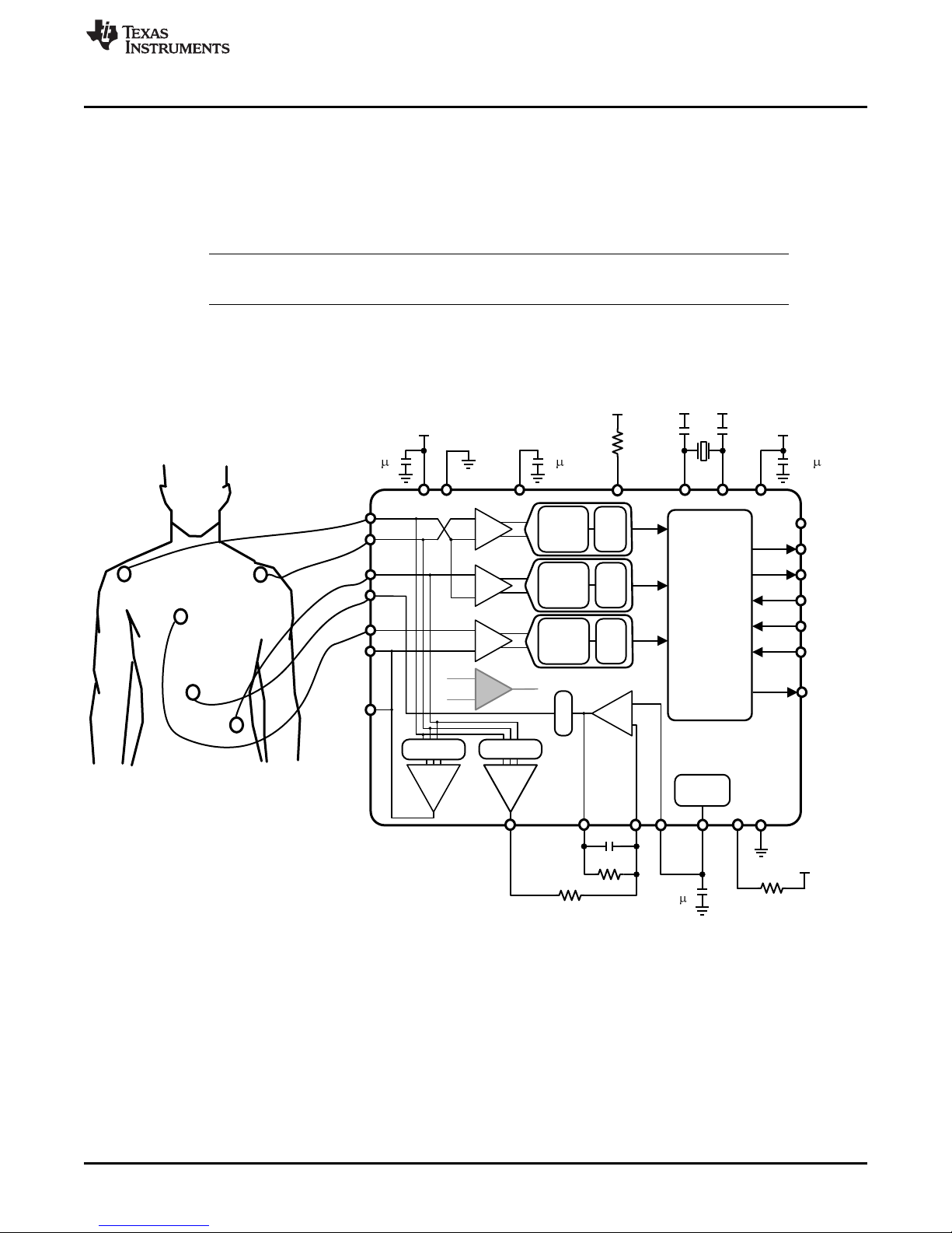
3 Theory of Operation
3.1 5-Lead ECG Application
Figure 5 shows the ADS1293 device in a 5-Lead ECG system setup. The ADS1293 device uses the
Common-Mode Detector to measure the common-mode of the patient’s body by averaging the voltage of
input pins IN1, IN2 and IN3, and uses this signal in the right leg drive feedback circuit.
NOTE: The ideal values of R1, R2and C1will vary per system/application; typical values for these
components are: R1= 100kΩ, R2= 1MΩ and C1= 1.5nF.
The output of the RLD amplifier is connected to the right leg electrode, which is IN4, to drive the commonmode of the patient’s body. The Wilson Central Terminal is generated by the ADS1293 and is used as a
reference to measure the chest electrode, V1. The chip uses an external 4.096MHz crystal oscillator
connected between the XTAL1 and XTAL2 pins to create the clock sources for the device.
Theory of Operation
CC2541 Communication
The CC2541 device communicates to the ADS1293 device through SPI interface. The CC2541 device
implements the application software to run this application through the 8051 microcontroller core in
addition to running the BLE stack. For additional information, see Section 4.4.
Figure 5. 5-Lead ECG Application
TIDU195A–January 2014–Revised July 2014 Wireless Heart Rate Monitor Reference Design
Submit Documentation Feedback
Copyright © 2014, Texas Instruments Incorporated
9
Page 10
Theory of Operation
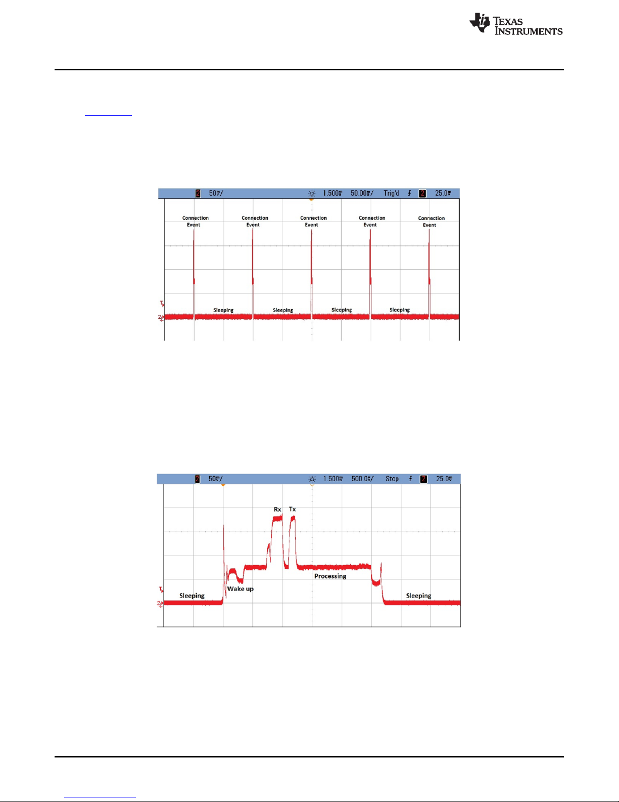
3.2 Battery Life Calculation
For battery life calculations, TI highly recommends that the user reviews CC2541 Battery Life Calculation,
SWRA347.
Comparing the power consumption of a BLE device to another device using a single metric is impossible.
For example, a device gets rated by its peak current. While the peak current plays a part in the total power
consumption, a device running the BLE stack only consumes current at the peak level during
transmission. Even in very high throughput systems, a BLE device is transmitting for only a small
percentage of the total time that the device is connected (see Figure 6).
www.ti.com
Figure 6. Current Consumption
In addition to transmitting, there are other factors to consider when calculating battery life. A BLE device
can go through several other modes, such as receiving, sleeping, and waking up from sleep. Even if the
current consumption of a device in each different mode is known, there is not enough information to
determine the total power consumed by the device. Each layer of the BLE stack requires a certain amount
of processing to remain connected and to comply with the specifications of the protocol. The MCU takes
time to perform this processing, and during this time, current is consumed by the device. In addition, some
power might be consumed while the device switches between modes (see Figure 7). All of this must be
considered to get an accurate measurement of the total current consumed.
Figure 7. Current Consumption-Active versus Sleep Modes
10
Wireless Heart Rate Monitor Reference Design TIDU195A–January 2014–Revised July 2014
Copyright © 2014, Texas Instruments Incorporated
Submit Documentation Feedback
Page 11
www.ti.com
4 Getting Started
4.1 Software
Requirements:
• An iOS device: iPhone 4S and newer generations; iPad 3 and newer generations; fifth generation iPod
(www.Apple.com)
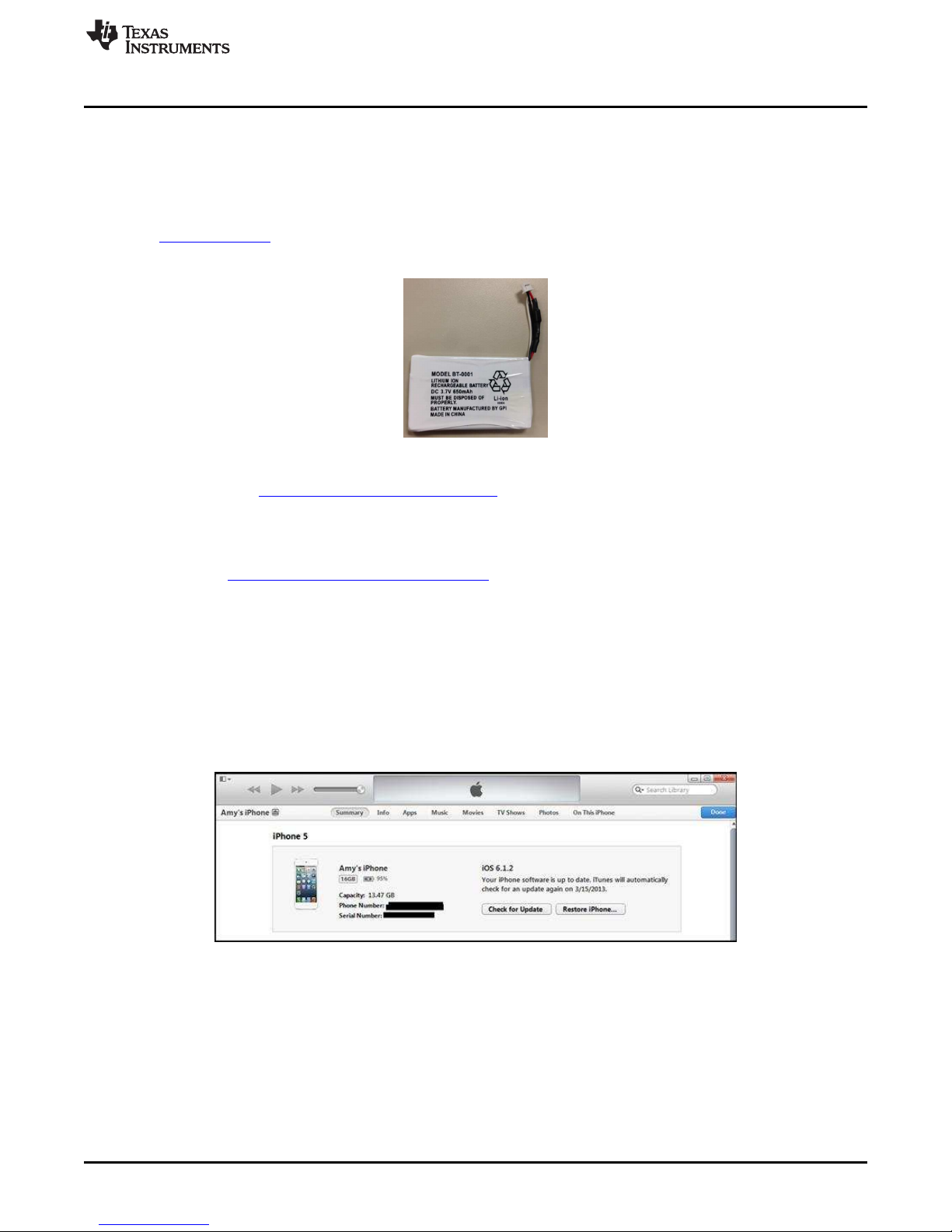
• 3.6-V Lithium-ion battery, recommended model BT-0001
• CC Debugger (http://www.ti.com/tool/cc-debugger)
4.1.1 Installing the Application
The application is not on iTunes (Apple Approved) for download. Download the application from the
following link: TIDA-00096 iOS Application Software .
Since the application is not on iTunes, use the steps below to install it manually. When the application is
distributed manually, there is a limit on how many devices can the application can be loaded on. The
UDID of each device needs to be provided before the application can be installed.
Use the following steps to install the Wireless Heart Rate Monitor application on a device.
1. Connect the iPhone or iPad to the PC.
2. Open the iTunes application on the PC.
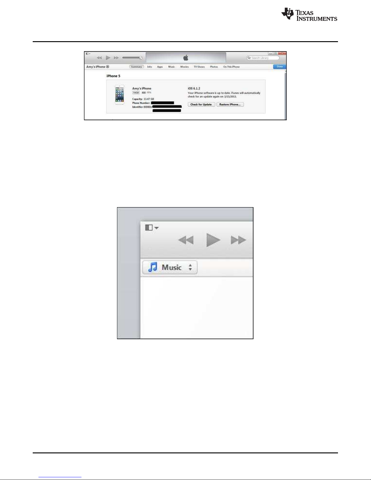
3. Wait for iTunes to identify that the device is connected to the PC.
4. The serial number of the device is listed as shown in Figure 9.
Getting Started
Figure 8. 3.6-V Lithium-Ion Battery
5. In order to view the Identifier number (UDID), double click on Serial Number as shown in Figure 10
TIDU195A–January 2014–Revised July 2014 Wireless Heart Rate Monitor Reference Design
Submit Documentation Feedback
Figure 9. Opening iTunes
11
Copyright © 2014, Texas Instruments Incorporated
Page 12
Getting Started
6. Report the identifier number (UDID) number to the iPad developer.
7. After the UDID is added to the application (by the iPad developer), a .zip file is sent to the iTunes user
that contains the application to download onto the smart device such as an iPhone4S®, iPhone 5®, or
iPad4®.
8. Unzip the folder to view the application, ecgmonitor.ipa.
9. Open iTunes
Once iTunes is open, use the following steps to install the application on the device.
1. Click the top-left button in the iTunes interface shown in Figure 11.
www.ti.com
Figure 10. Finding the UDID Number
2. Once the top-left button is clicked, a menu appears, click on Add File to Library (see Figure 12) to
navigate to and select the ecgmonitor.ipa file from the file directory.
12
Wireless Heart Rate Monitor Reference Design TIDU195A–January 2014–Revised July 2014
Figure 11. iTunes library
Copyright © 2014, Texas Instruments Incorporated
Submit Documentation Feedback
Page 13

www.ti.com
Getting Started
Figure 12. Add File to Library
TIDU195A–January 2014–Revised July 2014 Wireless Heart Rate Monitor Reference Design
Submit Documentation Feedback
13
Copyright © 2014, Texas Instruments Incorporated
Page 14

Getting Started
3. Go to the iPad page and click on the Apps menu as shown in Figure 13.
www.ti.com
4. Click on Install and then click Apply. Next, click on Sync. Then finally click Done.
4.2 Hardware
Use to following steps to connect the Demo board.
1. Connect the battery (3.6 V nominal) to the P1 connector on the ADS1293BLE board.
2. Set the U2 switch to the ON position.
3. Uninstall J3.
4. Connect the ECG cable to the J1 connector on the ADS1293BLE board (see Figure 14).
5. Connect the five leads to either an ECG simulator or to five electrode pads attached to the body. On
the back of each lead is a label (RL, LL, LA, RA, and V1).
Figure 13. Installing the Application on the iOS Device
Figure 14. Hardware Setup
NOTE: For the SKX2000 simulators connect V1 to the C1 terminal. If using the SKX2000 simulator,
turn the simulator on and off by pressing the red button on the left side (see Figure 15).
14
Wireless Heart Rate Monitor Reference Design TIDU195A–January 2014–Revised July 2014
Copyright © 2014, Texas Instruments Incorporated
Submit Documentation Feedback
Page 15

www.ti.com
Getting Started
4.3 Running the Demo
• Open up the ADS1293 ECG monitor application on either an iPad or iPhone.
• Press the Start Scanning button as shown in Figure 17.
Figure 15. ECG Emulator
Figure 16. ECG Monitor Application
TIDU195A–January 2014–Revised July 2014 Wireless Heart Rate Monitor Reference Design
Submit Documentation Feedback
Figure 17. Launch Application
15
Copyright © 2014, Texas Instruments Incorporated
Page 16

Getting Started
• After several moments, the ADS1293 ECG Demo START button and the Bluetooth symbol appear as
shown in Figure 18.
NOTE: If the Bluetooth symbol does not appear, close the application and repeat the steps listed in
• The three channel readings are now available on the screen. If the board and ECG simulator are
properly connected, the screen will appear similar to Figure 19 or Figure 20.
– Figure 19 appears when connected to SKX2000 ECG Simulator.
www.ti.com
Section 4.3. If the problem continues, see Section 5 below.
Figure 18. Enable Bluetooth on iOS Device
Figure 19. ECG Data Connected to the Simulator
– Figure 20 appears when connected to the body.
Figure 20. ECG Data Connected to the Body
16
Wireless Heart Rate Monitor Reference Design TIDU195A–January 2014–Revised July 2014
Copyright © 2014, Texas Instruments Incorporated
Submit Documentation Feedback
Page 17

www.ti.com
4.4 Firmware
This section describes the over-the-air protocol to be used in the Wireless Heart Rate Monitor Reference
Design. This section also provides an overview of the firmware development platform.
To download the software and firmware, go to TIDA-00096.
• iOS source code
• CC2541 BLE source code
4.4.1 Communication Overview
ECG data is sent as a burst of six BLE-notification packets every 14 ms. Each notification packet consists
of 20 bytes containing the following:
• ECG Sample1 (Raw ADC data)
– Channel1 (3 bytes)
– Channel2 (3 bytes)
– Channel3 (3 bytes)
• ECG Sample2 (Raw ADC data)
– Channel1 (3 bytes)
– Channel2 (3 bytes)
– Channel3 (3 bytes)
An ECG error or status packet is sent once every 17 ECG samples. ECG status packets contain the
following:
• 2-byte running counter
• Status packet begin indication: 0xFF, 0xFF, 0xFF
• 7-byte error status (ERROR_LOD, ERROR_STATUS, ERROR_RANGE1, ERROR_RANGE2,
ERROR_RANGE3, ERROR_SYNC, ERROR_MISC)
• Status packet end: 0xFF, 0xFF, 0xFF, 0xFF, 0xFF, 0xFF, 0xFF, 0xFF
Getting Started
4.4.2 ADS1293 ECG Demo: Complete Attribute Table
Figure 21 shows the complete attribute table for the ADS1293 ECG-Demo. Services are shown in yellow,
characteristics are shown in blue, and characteristic values and descriptors are shown in grey. The
ADS1293 ECG demo implements a BLE peripheral device. The Demo supports an ECG peripheral profile
based on the heart rate example of the CC254x Simple BLE Peripheral frame work.
When configured by a peer device, the ECG peripheral application sends notification of the ECG
measurement. On power up, advertising is enabled and the peer device must discover and initiate a
connection procedure to the ECG peripheral. When the peer device configures the ECG measurement for
notification, a timer starts and ECG measurements are sent periodically. In addition to ECG measurement,
the peer device can read the number of ECG channels supported (characteristic 2) and the number of
ECG-sample data sets per packet (characteristic 3).
The peer device may also discover and configure the battery service for battery level-state notifications.
This functionality is the same as supported in Simple BLE Peripheral framework.
TIDU195A–January 2014–Revised July 2014 Wireless Heart Rate Monitor Reference Design
Submit Documentation Feedback
17
Copyright © 2014, Texas Instruments Incorporated
Page 18

handle (he x) Type (hex ) Type Hex / Text Value (default)
GATT Server
Permissi ons
Notes
0x10 0x2800 GATT_PRIMARY_SERVICE_UUID 0x2D0D (ECG_SERV_UUID) GATT_PERMIT_READ
Start of ECG Profile
Service
10( properties: notify only)
12 00( handle: 0x0012)
37 2D (UUID: 0x2D37)
0x12 0x2D37 ECG_MEAS_UUID
00:00:00:00:00:00:00:00:00:00:00:00 (12
bytes)
(none) ECG data value
0x13 0x2902 GATT_CLIENT_CHAR_CFG_UUID 00:00 (2 bytes)
GATT_PERMIT_READ |
GATT_PERMIT_WRITE
Write "01:00" to enable
notifi cations. "00:00" to
disable
0x14 0x2901 GATT_CHAR_USER_DESC_UUID "ECG Measurement Data\0"(21 bytes) GATT_PERMIT_READ
Characteristic1 user
description
02( properties: read only)
16 00( handle: 0x0016)
38 2D (UUID: 0x2D38)
0x16 0x2D38 ECG_NUM_CHANS 03 (1 byte) GATT_PERMIT_READ
Number of ECG
Channels
0x17 0x2901 GATT_CHAR_USER_DESC_UUID "N umber of ECG Channels\0" (23by tes) GATT_PERMIT_READ
Characteristic3 user
description
02( properties: read only)
19 00( handle: 0x0019)
39 2D (UUID: 0x2D39)
0x19 0x2D39 ECG_SAMPLE_SETS 01 (1 byte) GATT_PERMIT_READ
Number of ECG Sample
Sets per packet
0x1A 0x2901 GATT_CHAR_USER_DESC_UUID
"ECGS ample Sets Per Packet\0" (27
bytes)
GATT_PERMIT_READ
Characteristic3 user
description
08 (properties: write onl y)
1C 00 (handle: 0x001C)
3A 2D (UUID: 0x2D3A)
0x1C 0x2D3A ECG_COMMAND 00 (1 byte) GATT_PERMIT_READ ECG command set
0x1B 0x2803 ECG_PROFILE_CHARACTER4_UUID GATT_PERMIT_WRITE
Characteristic4
declaration
0x15 0x2803 ECG_PROFILE_CHARACTER2_UUID GATT_PERMIT_READ
Characteristic2
declaration
0x18 0x2803 ECG_PROFILE_CHARACTER3_UUID GATT_PERMIT_READ
Characteristic3
declaration
ECG Peripheral Appli cation: Complete Attri bute Table
0x11 0x2803 ECG_PROFILE_CHARACTER1_UUID GATT_PERMIT_READ
Characteristic1
declaration
Getting Started
www.ti.com
Figure 21. ECG Peripheral Application: Complete Attribute Table
18
Wireless Heart Rate Monitor Reference Design TIDU195A–January 2014–Revised July 2014
Copyright © 2014, Texas Instruments Incorporated
Submit Documentation Feedback
Page 19

ECG Sample1 Data
Running Counter
www.ti.com
4.4.3 ECG Notification Packet
Figure 22 shows an example of captured ECG notification packets.
Table 1 lists the ECG notification data consisting of 20 bytes and the format.
Getting Started
Figure 22. ECG Notification Packet
Table 1. ECG Notification Data Format
Byte Number Default Value Description
0 xxxx Running Counter – High byte
1 xxxx Running Counter – Low byte
2 0xD1 ECG Sample1: Channel 1 ADC High byte
3 0xD2 ECG Sample1: Channel 1 ADC Middle byte
4 0xD3 ECG Sample1: Channel 1 ADC Low byte
5 0xD4 ECG Sample1: Channel 2 ADC High byte
6 0xD5 ECG Sample1: Channel 2 ADC Middle byte
7 0xD6 ECG Sample1: Channel 2 ADC Low byte
8 0xD7 ECG Sample1: Channel 3 ADC High byte
9 0xD8 ECG Sample1: Channel 3 ADC Middle byte
10 0xD9 ECG Sample1: Channel 3 ADC Low byte
11 0xD1 ECG Sample2: Channel 1 ADC High byte
12 0xD2 ECG Sample2: Channel 1 ADC Middle byte
13 0xD3 ECG Sample2: Channel 1 ADC Low byte
14 0xD4 ECG Sample2: Channel 2 ADC High byte
15 0xD5 ECG Sample2: Channel 2 ADC Middle byte
16 0xD6 ECG Sample2: Channel 2 ADC Low byte
17 0xD7 ECG Sample2: Channel 3 ADC High byte
18 0xD8 ECG Sample2: Channel 3 ADC Middle byte
19 0xD9 ECG Sample2: Channel 3 ADC Low byte
(1)
The Allowed maximum size of notification packet is 20 bytes.
(1)
TIDU195A–January 2014–Revised July 2014 Wireless Heart Rate Monitor Reference Design
Submit Documentation Feedback
19
Copyright © 2014, Texas Instruments Incorporated
Page 20

Getting Started
4.4.4 Connection Setup
Bluetooth low-energy uses a 20-ms connection interval. Twenty user-data bytes (which is equal to 2samples for each channel and 2-bytes running counter) are sent in GATT notifications. Data from
ADS1293 device is ping-pong buffered and up to six notifications are sent every 14 ms based on an OSAL
timer. The ADS1293 sample rate is set as 160 samples/sec (SPS) (see the ADS1293 data sheet,
SNAS602, for more information on R1 = 4, R2 = 5, and R3 = 32). Each sample is 3 bytes and is sending 3
channels.
Firmware Development Platform
One of the development platforms for the CC2541 8051 microcontroller is the IAR development platform.
For information on this platform, goto http://www.iar.com. To communicate to the development platform
through IAR, the CC Debugger is required as shown in Figure 23
The CC Debugger (shown in Figure 23) must be connected to the 10-pin header on the SAT0015 board.
Ensure the notch on the cable that connects to the 10-pin header is towards the outside. If connected
properly, the LED on the CC Debugger lights green.
www.ti.com
Figure 23. CC Debugger
Launch the IAR project workspace as shown in Figure 24.
Figure 24. Project Details.
20
Wireless Heart Rate Monitor Reference Design TIDU195A–January 2014–Revised July 2014
Copyright © 2014, Texas Instruments Incorporated
Submit Documentation Feedback
Page 21

www.ti.com
Ensure that the software is on version 8.20.1 or newer as shown in Figure 25.
Getting Started
Figure 25. Version Control
Figure 26 shows the main entry function.
Figure 26. Main Function
TIDU195A–January 2014–Revised July 2014 Wireless Heart Rate Monitor Reference Design
Submit Documentation Feedback
21
Copyright © 2014, Texas Instruments Incorporated
Page 22

Common Issues and Solutions
Figure 27 shows the various communication settings for the application.
Figure 28 shows that all of the key-configuration settings for the ADS1293 device are easily updated
through the single function.
www.ti.com
Figure 27. Key Parameters
5 Common Issues and Solutions
Issue —The iPad or iPhone will not connect to the demo through Bluetooth.
Solution: Ensure that the application is shut down completely before trying to reconnect. To shut
down the application, hold the home button on the iPad or iPhone until the task manager window
appears. This window shows all of the applications running in the background. Press and hold on
the ADS1293 application until the X or - symbol appears. Click the X or - to completely shut down
the application. Start again to reconnect the demo board. If the issue continues, see the following
solution on adjusting the input voltage from the battery.
22
Wireless Heart Rate Monitor Reference Design TIDU195A–January 2014–Revised July 2014
Figure 28. Key Configuration Settings
Copyright © 2014, Texas Instruments Incorporated
Submit Documentation Feedback
Page 23

0
500
1000
1500
2000
2500
3000
3500
-6
-4.2
-2.4
-0.6
1.2 3 4.8
6.6
8.4
10.2
12
Occurrences
Input-Referred Noise (µV)
C006
VDDIO = 3.3 V
-15
-10
-5
0
5
10
15
0 1 2 3 4 5 6 7 8 9 10
Input-Referred Noise (µV)
Time (s)
C004
VDDIO = 3.3 V
www.ti.com
6 Test Data and Simulation Results
6.1 Antenna Simulations
The following data was simulated using the High-Frequency Structural Simulator (HFSS) from ANSYS
(www.ansys.com).
The goal of the antenna simulations was to validate that the 2.45-GHz antenna performed as expected.
Test Data and Simulation Results
6.2 Noise Test Results
Figure 30 and Figure 31 show the input referred noise of the AFE.
Figure 29. Antenna Simulation
Figure 30. Input-Referred Noise
Figure 31. Noise Histogram
TIDU195A–January 2014–Revised July 2014 Wireless Heart Rate Monitor Reference Design
Submit Documentation Feedback
23
Copyright © 2014, Texas Instruments Incorporated
Page 24

-180
-160
-140
-120
-100
-80
-60
-40
-20
0
0 40 80 120 160 200 240
Amplitude (dBFS)
Frequency (Hz)
C007
Data Rate = 1067 SPS
ECG BW = 215 Hz
VDDIO = 3.3 V
-180
-160
-140
-120
-100
-80
-60
-40
-20
0
0 400 800 1200 1600 2000 2400
Amplitude (dBFS)
Frequency (Hz)
C008
Data Rate = 25.6k SPS
PACE BW = 2550 Hz
VDDIO = 3.3 V
Test Data and Simulation Results
6.3 FFT Results
Figure 32 and Figure 33 show the FFT results of the ADS1293 device corresponding to different peak
rates.
Figure 32. FFT Plot ECG Channel Figure 33. FFT Plot Pace Channel
(50-Hz Signal) (50-Hz Signal)
6.4 EMI Test Results of the ADS1293
www.ti.com
DUT Frequency MHz Vos_Off (uV) Vos_On (uV) Vrf_pp (mV) EMIRR
4L2 400 -4.94 -4.93 130.8 132.6231099
4L2 900 -4.82 -5 103.4 103.4341716
4L2 1800 -5.05 -4.98 90 109.2265398
4L2 2400 -4.95 -4.9 45.2 100.1849375
6L1 400 19.03 18.99 218.1 129.463827
6L1 900 19 18.97 225.6 132.5499389
6L1 1800 19 18.98 185.7 132.6906764
6L1 2400 19.01 18.99 41.9 106.8267612
11L1 400 -4.55 -4.36 204.1 114.7774483
11L1 900 -4.38 -4.26 204.8 118.8283733
11L1 1800 -4.39 -4.48 147.2 115.5902624
11L1 2400 -4.42 -4.37 47.73 101.1310575
24
Wireless Heart Rate Monitor Reference Design TIDU195A–January 2014–Revised July 2014
Table 2. Test Results
Copyright © 2014, Texas Instruments Incorporated
Submit Documentation Feedback
Page 25

www.ti.com
Test Data and Simulation Results
Figure 34. Setup for ECG Data
Figure 35. ECG Data as Shown on an iOS Device
FCC Compliance
The Wireless Heart Rate Monitor Reference Design platform uses a similar RF design (antenna design)
that complied with the following standards:
• EN 300 328
• FCC 15.247
• IC RSS-210
• EN 301 489-17
FCC and IC Regulatory Compliance standards:
– FCC – Federal Communications Commission Part 15, Class A
– IC – Industry Canada ICES-003 Class A
See the Gas Sensor Platform Reference Design (SNOA922) for reference.
TIDU195A–January 2014–Revised July 2014 Wireless Heart Rate Monitor Reference Design
Submit Documentation Feedback
25
Copyright © 2014, Texas Instruments Incorporated
Page 26

V_Lithium
Li ION Battery (1s) UNIDEN 3.6V 720mA h 1 inchX2inch
VDD_3 = V_Lithium (if V_Lithium>3V) VDD_3 = 3V (if V_Lithium<3V)
V_Lithium
123
P1
0.47V
D2
SBR0220T5-7-F
0.1µF
C20
10µF
C22
47µF
C21
2
1
5
3
4
6
U2
EG1390B
VIN
1
FB
2
GND
3
VOUT
4
L
5
EN
6
U3
TPS61220DCK
VDD_3
1.00Meg
R16
200k
R17
10µF
C23
4.7µH
L5
EPL3015-472MLB
Schematics
www.ti.com
7 Schematics
Figure 36. Power Section
26
Wireless Heart Rate Monitor Reference Design TIDU195A–January 2014–Revised July 2014
Submit Documentation Feedback
Copyright © 2014, Texas Instruments Incorporated
Page 27

VDD_3
VDD_3
VDD_3
VDD_3
22pF
C6
22pF
C31
VDD_3
VDD_3
VDD_3
CVREF
1µF
C3
MISO
MOSI
C
SS
DRDYB
ALARMB
1nF
C5
10k
R15
10.0Meg
R32
1.0Meg
R34
1.0Meg
R35
1.0Meg
R1
1.0Meg
R14
51
R2
51
R4
RSTB_1293
0.1µF
C4
0.1µF
C7
0.1µF
C1
0.1µF
C2
0
R36
0
R5
0
R6
0
R9
0
R11
0
R12
1
2
3
4
5
6
7
8
9
11
10
J1
1734348-1
CMOUT
RLDOUT
RLDIN
RLDINIV
WCT
CLK
V1
RL
LL
LA
RA
RA
LA
LL
RL
V1
1
2
4.096MHz
Y1
ECS-41-18-5PXEN-TR
IN1
1
IN2
2
IN3
3
IN4
4
IN5
5
IN6
6
WCT
7
CMOUT
8
RLDOUT
9
RLDINV
10
RLDIN
11
RLDREF
12
SYNCB
13
VSSIO
14
ALARMB
15
CSB
16
SCLK
17
SDI
18
SDO
19
DRDYB
20
CLK
21
VDDIO
22
XTAL1
23
XTAL2
24
RSTB
25
CVREF
26
VSS
27
VDD
28
PAD
U1
ADS1293CISQE/NOPB
1 2
S1
PTS635SL50LFS
www.ti.com
Schematics
Figure 37. Analog Front End
27
TIDU195A–January 2014–Revised July 2014 Wireless Heart Rate Monitor Reference Design
Submit Documentation Feedback
Copyright © 2014, Texas Instruments Incorporated
Page 28

VDD_3
VDD_FILT
SoC Debug/Flash
VDD_FILT
1
2
A3
ANTENNA IIFABLE
SS
C
MOSI
V_Lithium
SPI BUS TOADS1293
MISO
ALARMB
DRDYB
RSTB_1293
2.00Meg
R13
3.01Meg
R21
1
2
J3
0
R3
0
R18
0
R19
0
R37
0
R28
0
R30
0
R29
0
R20
0
R31
0
R26
0
R22
0
R25
0
R8
0
R40
2.21k
R24
2.74k
R10
0.1µF
C25
0.1µF
C26
0.1µF
C27
0.1µF
C28
0.1µF
C30
2.2µF
C8
220pF
C29
12pF
C17
12pF
C18
15pF
C14
15pF
C16
18pF
C11
18pF
C12
1pF
C9
1pF
C13
1µF
C24
1µF
C15
1000pF
C19
1293_RSTB
BLE_RST
RESET_N
P0_5/SCK
P0_4/SSN
P0_3/MISO
P0_2/MOSI
BLE_RST
P2_1/DD
1293_RSTB
P2_1/DD
P2_2/DC
PULSE_BEAT
PULSE_BEAT
56.2k
R23
0.4pF
C10
1000 ohm
FB1
5.1nH
L2
LQG15HH5N1S02D
2nH
L3
LQG15HS2N0S02D
2nH
L4
LQG15HS2N0S02D
1 2
32.768kHz
X1
ABS07-32.768KHZ-9-T
1
3 4
2
G
G
32MHz
X2
Q22FA1280009200
GND
1
SCL
2
SDA
3
NC
4
P1_5
5
P1_4
6
P1_3
7
P1_2
8
P1_1
9
DVDD2
10
P1_0
11
P0_7
12
P0_6
13
P0_5
14
P0_4
15
P0_3
16
P0_2
17
P0_1
18
P0_0
19
RESET_N
20
AVDD6
31
XOSC_Q1
22
XOSC_Q2
23
AVDD5
21
RF_P
25
RF_N
26
AVDD4
29
AVDD3
24
AVDD2
27
RBIAS
30
AVDD1
28
P2_4
32
P2_3
33
P2_2
34
P2_1
35
P2_0
36
P1_7
37
P1_6
38
DVDD1
39
DCOUPL
40
THERM_PAD
41
U4
CC2541RHA
1
2
3
4
5
6
7
8
9
10
J2
CONN_FTSH-105-01-L-DV
0
R7
P0_2/MOSI
P0_3/MISO
RESET_N
P0_5/SCK
P0_4/SSN
P2_2/DC
GND
2.2nH
L1
LQG15HS2N2S02D
Yellow
D1
1 2
S2
PTS635SL50LFS
Schematics
www.ti.com
Figure 38. ADS1293 Section
28
Wireless Heart Rate Monitor Reference Design TIDU195A–January 2014–Revised July 2014
Submit Documentation Feedback
Copyright © 2014, Texas Instruments Incorporated
Page 29

www.ti.com
Bill of Materials
8 Bill of Materials
To download the bill of materials (BOM) for each board, see the design files at TIDA-00096. Table 3 lists the BOM.
Table 3. BOM
Designator Quantity Value Description PackageReference PartNumber Manufacturer
!PCB 1 Printed Circuit Board SAT0015 Any
C1, C2, C4, C7 4 0.1 µF CAP,CERM, 0.1 µF, 25 V, ±5%, X7R, 0603 0603 06033C104JAT2A AVX
C3 1 1 µF CAP, CERM, 1 µF, 16 V, ±10%, X5R, 0805 0805 0805YD105KAT2A AVX
C5 1 1000 pF CAP, CERM, 1000 pF, 100 V, ±5%, C0G/NP0, 0603 C1608C0G2A102J TDK
0603
C6, C31 2 22pF CAP, CERM, 22 pF, 50 V, ±5%, C0G/NP0, 0603 0603 06035A220JAT2A AVX
C8 1 2.2 µF CAP, CERM, 2.2 µF, 6.3 V, ±20%, X5R, 0402 0402 JMK105BJ225MV-F Taiyo Yuden
C9, C13 2 1pF CAP, CERM, 1 pF, 50 V, ±5%, C0G/NP0, 0402 0402 GRM1555C1H1R0CA01D MuRata
C10 1 0.4pF CAP, CERM, 0.4 pF, 50 V, ±25%, C0G/NP0, 0402 GRM1555C1HR40BA01D MuRata
0402
C11, C12 2 18 pF CAP, CERM, 18 pF, 50 V, ±5%, C0G/NP0, 0402 0402 GRM1555C1H180JA01D MuRata
C14, C16 2 15 pF CAP, CERM, 15 pF, 50 V, ±5%, C0G/NP0, 0402 0402 GRM1555C1H150JA01D MuRata
C15, C24 2 1 µF CAP, CERM, 1 µF, 6.3 V,±20%, X5R, 0402 0402 C1005X5R0J105M TDK
C17, C18 2 12 pF CAP, CERM, 12 pF, 50 V, ±5%, C0G/NP0, 0402 0402 GRM1555C1H120JA01D MuRata
C19 1 1000pF CAP, CERM, 1000 pF, 50 V, ±5%, C0G/NP0, 0402 GRM1555C1H102JA01D MuRata
0402
C20, C25, C26, 6 0.1µF CAP, CERM, 0.1 µF, 10 V, ±10%, X7R, 0402 0402 GRM155R71A104KA01D MuRata
C27, C28, C30
C21 1 47µF CAP, CERM, 47 µF, 6.3 V, ±10%, X5R, 1206 1206 GRM31CR60J476KE19L MuRata
C22, C23 2 10 µF CAP, CERM, 10 µF, 6.3 V, ±20%, X5R, 0603 0603 GRM188R60J106ME47D MuRata
C29 1 220pF CAP, CERM, 220 pF, 50 V, ±5%, C0G/NP0, 0402 0402 GRM1555C1H221JA01D MuRata
D1 1 Yellow LED, Yellow, SMD Yellow LED SML-P12YTT86 RΩ
D2 1 0.47V Diode, Schottky, 20 V, 0.2 A, SOD-523 SOD-523 SBR0220T5-7-F Diodes Inc.
FB1 1 1000Ω 0.25A Ferrite Bead, 1000 Ω at 100 MHz, SMD 0402 BLM15HG102SN1D MuRata
J1 1 Conn D-SUB RCPT R/A 9POS GOLD/FL, TH D-SUB 9 PIN 1734348-1 TE Connectivity
J2 1 FTSH-105-01- Header, 2 × 5 pin 50 mil spacing 0.222 × 0.330 inch FTSH-105-01-L-DV Samtec
L-DV
J3 1 Header, TH, 100mil, 2 × 1, Gold plated, 230 mil TSW-102-07-G-S TSW-102-07-G-S Samtec, Inc.
above insulator
L1 1 2.2nH Inductor, Multilayer, Air Core, 2.2 nH, 0.3 A, 0.12 0402 polarized LQG15HS2N2S02D MuRata
Ω, SMD
L2 1 5.1nH Inductor, Multilayer, Ferrite, 5.1 nH, 0.3 A, 0.2 Ω, 0402 LQG15HH5N1S02D MuRata
SMD
29
TIDU195A–January 2014–Revised July 2014 Wireless Heart Rate Monitor Reference Design
Submit Documentation Feedback
Copyright © 2014, Texas Instruments Incorporated
Page 30

Bill of Materials
www.ti.com
Table 3. BOM (continued)
Designator Quantity Value Description PackageReference PartNumber Manufacturer
L3, L4 2 2nH Inductor, Multilayer, Ferrite, 2 nH, 0.3 A, 0.1 Ω, 0402 LQG15HS2N0S02D MuRata
SMD
L5 1 4.7uH Inductor, Shielded, Ferrite, 4.7 µH, 1.2 A, 0.14 Ω, Inductor, 3 × 1,55 × EPL3015-472MLB Coilcraft
SMD 3 mm
P1 1 Header, 3-Pin, Right Angle 0530480310 Molex
R1, R14, R34, R35 4 1.0Meg RES, 1 MΩ, 5%, 0.063 W, 0402 0402 CRCW04021M00JNED Vishay-Dale
R2, R4 2 51 RES, 51 Ω, 5%, 0.063 W, 0402 0402 CRCW040251R0JNED Vishay-Dale
R3, R5, R6, R7, 21 0 RES, 0 Ω, 5%, 0.063 W, 0402 0402 CRCW04020000Z0ED Vishay-Dale
R8, R9, R11, R12,
R18, R19, R20,
R22, R25, R26,
R28, R29, R30,
R31, R36, R37,
R40
R10 1 2.74k RES, 2.74 kΩ, 1%, 0.063 W, 0402 0402 CRCW04022K74FKED Vishay-Dale
R13 1 2Meg RES, 2 MΩ, 1%, 0.063 W, 0402 0402 CRCW04022M00FKED Vishay-Dale
R15 1 10k RES, 10 kΩ, 5%, 0.063 W, 0402 0402 CRCW040210K0JNED Vishay-Dale
R16 1 1Meg RES, 1 MΩ, 1%, 0.063 W, 0402 0402 CRCW04021M00FKED Vishay-Dale
R17 1 200k RES, 200 kΩ, 1%, 0.063 W, 0402 0402 CRCW0402200KFKED Vishay-Dale
R21 1 3.01Meg RES, 3.01 MΩ, 1%, 0.063 W, 0402 0402 CRCW04023M01FKED Vishay-Dale
R23 1 56.2k RES, 56.2k Ω, 1%, 0.063 W, 0402 0402 CRCW040256K2FKED Vishay-Dale
R24 1 2.21k RES, 2.21k Ω, 1%, 0.063 W, 0402 0402 CRCW04022K21FKED Vishay-Dale
R32 1 10Meg RES, 10 MΩ, 1%, 0.063 W, 0402 0402 CRCW040210M0FKED Vishay-Dale
S1, S2 2 Switch, tactile, SPST-NO, 0.05 A, 12V, TH SW, SPST 3,5 × 5 PTS635SL50LFS C&K Components
mm
U1 1 ADS1293 low power, 3-channel, 24-bit analog RSG0028A ADS1293CISQE/NOPB Texas Instruments
front-end for Biopotential measurements,
RSG0028A
U2 1 Slide switch DPDT 0.3 A, SMT 7,2 × 3,5 × 3,5 mm EG1390B E-Switch
U3 1 Low input voltage step-up converter in 6-pin SC- DCK0006A TPS61220DCK Texas Instruments
70 package, DCK0006A
U4 1 2.4-GHz Bluetooth low energy and proprietary RHA0040H CC2541RHA Texas Instruments
System-on-Chip, RHA0040H
X1 1 CRYSTAL, 32.768 KHZ, 9 pF, SMD 3,2 × 0.9 × 1,5 mm ABS07-32.768KHZ-9-T Abracon Corportation
X2 1 Crystal, 32 MHz, 10 pF, SMD Crystal, 2,6 × 0,5 × Q22FA1280009200 Epson
1,6 mm
Y1 1 Crystal, 4.096 MHz, 18 pF, SMD Crystal, 11,4 × 4,3 × ECS-41-18-5PXEN-TR ECS, Inc.
3,8 mm
30
Wireless Heart Rate Monitor Reference Design TIDU195A–January 2014–Revised July 2014
Submit Documentation Feedback
Copyright © 2014, Texas Instruments Incorporated
Page 31

www.ti.com
9 Layer Plots
To download the layer plots for each board, see the design files at TIDA-00096. Figure 39 shows the layer
plots.
Layer Plots
Figure 0. UNDEFINED
Figure 0. UNDEFINED Figure 0. UNDEFINED
Figure 0. UNDEFINED
Figure 0. UNDEFINED
Figure 0. UNDEFINED
Figure 39. Layer Plot
Figure 0. UNDEFINED
TIDU195A–January 2014–Revised July 2014 Wireless Heart Rate Monitor Reference Design
Submit Documentation Feedback
Figure 0. UNDEFINED
31
Copyright © 2014, Texas Instruments Incorporated
Page 32

Altium Project
10 Altium Project
To download the Altium project files for each board, see the design files at TIDA-00096. Figure 40,
Figure 41, Figure 42, and Figure 43 show the layout.
www.ti.com
Figure 40. All Layers
Figure 42. Ground Layer
Figure 41. Bottom Layer
Figure 43. Top Layer
32
Wireless Heart Rate Monitor Reference Design TIDU195A–January 2014–Revised July 2014
Copyright © 2014, Texas Instruments Incorporated
Submit Documentation Feedback
Page 33

www.ti.com
Gerber Files
11 Gerber Files
To download the Gerber files for each board, see the design files at TIDA-00096.
Figure 44. Fab Drawing
33
TIDU195A–January 2014–Revised July 2014 Wireless Heart Rate Monitor Reference Design
Submit Documentation Feedback
Copyright © 2014, Texas Instruments Incorporated
Page 34

Software Files
12 Software Files
To download the software files for the reference design, see the design files at TIDA-00096.
References
For additional references, please see the following:
1. Bluetooth Low Energy CC2540 Mini Development Kit User’s Guide, SWRU270
13 About the Author
AJINDER PAL SINGH is a Systems Architect at Texas Instruments where he is responsible for
developing reference design solutions for the industrial segment. Ajinder brings to this role his extensive
experience in high-speed digital, low-noise analog and RF system-level design expertise. Ajinder earned
his Master of Science in Electrical Engineering (MSEE) from Texas Tech University in Lubbock, TX.
Ajinder is a member of the Institute of Electrical and Electronics Engineers (IEEE).
NATARAJAN VISWANATHAN, also known as Vishy, is an Applications Engineer at Texas Instruments
Silicon Valley Analog where he is involved in developing embedded firmware, evaluation tools, and
customer demo systems. Vishy has broad experience with system on chips, microcontrollers, and
application processors. Vishy earned his Masters and PhD from the Indian Institute of Science, Bangalore.
www.ti.com
34
Wireless Heart Rate Monitor Reference Design TIDU195A–January 2014–Revised July 2014
Copyright © 2014, Texas Instruments Incorporated
Submit Documentation Feedback
Page 35

www.ti.com
Revision History
Revision History
Changes from Original (January 2014) to A Revision .................................................................................................... Page
• Changed to the correct name for the design........................................................................................... 3
• Added paragraph explaining that installation of application is manual, but the designer must still connect to iTunes to
install the application. ................................................................................................................... 11
NOTE: Page numbers for previous revisions may differ from page numbers in the current version.
TIDU195A–January 2014–Revised July 2014 Revision History
Submit Documentation Feedback
35
Copyright © 2014, Texas Instruments Incorporated
Page 36

STANDARD TERMS AND CONDITIONS FOR EVALUATION MODULES
1. Delivery: TI delivers TI evaluation boards, kits, or modules, including any accompanying demonstration software, components, or
documentation (collectively, an “EVM” or “EVMs”) to the User (“User”) in accordance with the terms and conditions set forth herein.
Acceptance of the EVM is expressly subject to the following terms and conditions.
1.1 EVMs are intended solely for product or software developers for use in a research and development setting to facilitate feasibility
evaluation, experimentation, or scientific analysis of TI semiconductors products. EVMs have no direct function and are not
finished products. EVMs shall not be directly or indirectly assembled as a part or subassembly in any finished product. For
clarification, any software or software tools provided with the EVM (“Software”) shall not be subject to the terms and conditions
set forth herein but rather shall be subject to the applicable terms and conditions that accompany such Software
1.2 EVMs are not intended for consumer or household use. EVMs may not be sold, sublicensed, leased, rented, loaned, assigned,
or otherwise distributed for commercial purposes by Users, in whole or in part, or used in any finished product or production
system.
2 Limited Warranty and Related Remedies/Disclaimers:
2.1 These terms and conditions do not apply to Software. The warranty, if any, for Software is covered in the applicable Software
License Agreement.
2.2 TI warrants that the TI EVM will conform to TI's published specifications for ninety (90) days after the date TI delivers such EVM
to User. Notwithstanding the foregoing, TI shall not be liable for any defects that are caused by neglect, misuse or mistreatment
by an entity other than TI, including improper installation or testing, or for any EVMs that have been altered or modified in any
way by an entity other than TI. Moreover, TI shall not be liable for any defects that result from User's design, specifications or
instructions for such EVMs. Testing and other quality control techniques are used to the extent TI deems necessary or as
mandated by government requirements. TI does not test all parameters of each EVM.
2.3 If any EVM fails to conform to the warranty set forth above, TI's sole liability shall be at its option to repair or replace such EVM,
or credit User's account for such EVM. TI's liability under this warranty shall be limited to EVMs that are returned during the
warranty period to the address designated by TI and that are determined by TI not to conform to such warranty. If TI elects to
repair or replace such EVM, TI shall have a reasonable time to repair such EVM or provide replacements. Repaired EVMs shall
be warranted for the remainder of the original warranty period. Replaced EVMs shall be warranted for a new full ninety (90) day
warranty period.
3 Regulatory Notices:
3.1 United States
3.1.1 Notice applicable to EVMs not FCC-Approved:
This kit is designed to allow product developers to evaluate electronic components, circuitry, or software associated with the kit
to determine whether to incorporate such items in a finished product and software developers to write software applications for
use with the end product. This kit is not a finished product and when assembled may not be resold or otherwise marketed unless
all required FCC equipment authorizations are first obtained. Operation is subject to the condition that this product not cause
harmful interference to licensed radio stations and that this product accept harmful interference. Unless the assembled kit is
designed to operate under part 15, part 18 or part 95 of this chapter, the operator of the kit must operate under the authority of
an FCC license holder or must secure an experimental authorization under part 5 of this chapter.
3.1.2 For EVMs annotated as FCC – FEDERAL COMMUNICATIONS COMMISSION Part 15 Compliant:
CAUTION
This device complies with part 15 of the FCC Rules. Operation is subject to the following two conditions: (1) This device may not
cause harmful interference, and (2) this device must accept any interference received, including interference that may cause
undesired operation.
Changes or modifications not expressly approved by the party responsible for compliance could void the user's authority to
operate the equipment.
FCC Interference Statement for Class A EVM devices
NOTE: This equipment has been tested and found to comply with the limits for a Class A digital device, pursuant to part 15 of
the FCC Rules. These limits are designed to provide reasonable protection against harmful interference when the equipment is
operated in a commercial environment. This equipment generates, uses, and can radiate radio frequency energy and, if not
installed and used in accordance with the instruction manual, may cause harmful interference to radio communications.
Operation of this equipment in a residential area is likely to cause harmful interference in which case the user will be required to
correct the interference at his own expense.
SPACER
SPACER
SPACER
SPACER
SPACER
SPACER
SPACER
SPACER
Page 37

FCC Interference Statement for Class B EVM devices
NOTE: This equipment has been tested and found to comply with the limits for a Class B digital device, pursuant to part 15 of
the FCC Rules. These limits are designed to provide reasonable protection against harmful interference in a residential
installation. This equipment generates, uses and can radiate radio frequency energy and, if not installed and used in accordance
with the instructions, may cause harmful interference to radio communications. However, there is no guarantee that interference
will not occur in a particular installation. If this equipment does cause harmful interference to radio or television reception, which
can be determined by turning the equipment off and on, the user is encouraged to try to correct the interference by one or more
of the following measures:
• Reorient or relocate the receiving antenna.
• Increase the separation between the equipment and receiver.
• Connect the equipment into an outlet on a circuit different from that to which the receiver is connected.
• Consult the dealer or an experienced radio/TV technician for help.
3.2 Canada
3.2.1 For EVMs issued with an Industry Canada Certificate of Conformance to RSS-210
Concerning EVMs Including Radio Transmitters:
This device complies with Industry Canada license-exempt RSS standard(s). Operation is subject to the following two conditions:
(1) this device may not cause interference, and (2) this device must accept any interference, including interference that may
cause undesired operation of the device.
Concernant les EVMs avec appareils radio:
Le présent appareil est conforme aux CNR d'Industrie Canada applicables aux appareils radio exempts de licence. L'exploitation
est autorisée aux deux conditions suivantes: (1) l'appareil ne doit pas produire de brouillage, et (2) l'utilisateur de l'appareil doit
accepter tout brouillage radioélectrique subi, même si le brouillage est susceptible d'en compromettre le fonctionnement.
Concerning EVMs Including Detachable Antennas:
Under Industry Canada regulations, this radio transmitter may only operate using an antenna of a type and maximum (or lesser)
gain approved for the transmitter by Industry Canada. To reduce potential radio interference to other users, the antenna type
and its gain should be so chosen that the equivalent isotropically radiated power (e.i.r.p.) is not more than that necessary for
successful communication. This radio transmitter has been approved by Industry Canada to operate with the antenna types
listed in the user guide with the maximum permissible gain and required antenna impedance for each antenna type indicated.
Antenna types not included in this list, having a gain greater than the maximum gain indicated for that type, are strictly prohibited
for use with this device.
Concernant les EVMs avec antennes détachables
Conformément à la réglementation d'Industrie Canada, le présent émetteur radio peut fonctionner avec une antenne d'un type et
d'un gain maximal (ou inférieur) approuvé pour l'émetteur par Industrie Canada. Dans le but de réduire les risques de brouillage
radioélectrique à l'intention des autres utilisateurs, il faut choisir le type d'antenne et son gain de sorte que la puissance isotrope
rayonnée équivalente (p.i.r.e.) ne dépasse pas l'intensité nécessaire à l'établissement d'une communication satisfaisante. Le
présent émetteur radio a été approuvé par Industrie Canada pour fonctionner avec les types d'antenne énumérés dans le
manuel d’usage et ayant un gain admissible maximal et l'impédance requise pour chaque type d'antenne. Les types d'antenne
non inclus dans cette liste, ou dont le gain est supérieur au gain maximal indiqué, sont strictement interdits pour l'exploitation de
l'émetteur
3.3 Japan
3.3.1 Notice for EVMs delivered in Japan: Please see http://www.tij.co.jp/lsds/ti_ja/general/eStore/notice_01.page 日本国内に
輸入される評価用キット、ボードについては、次のところをご覧ください。
http://www.tij.co.jp/lsds/ti_ja/general/eStore/notice_01.page
3.3.2 Notice for Users of EVMs Considered “Radio Frequency Products” in Japan: EVMs entering Japan are NOT certified by
TI as conforming to Technical Regulations of Radio Law of Japan.
If User uses EVMs in Japan, User is required by Radio Law of Japan to follow the instructions below with respect to EVMs:
1. Use EVMs in a shielded room or any other test facility as defined in the notification #173 issued by Ministry of Internal
Affairs and Communications on March 28, 2006, based on Sub-section 1.1 of Article 6 of the Ministry’s Rule for
Enforcement of Radio Law of Japan,
2. Use EVMs only after User obtains the license of Test Radio Station as provided in Radio Law of Japan with respect to
EVMs, or
3. Use of EVMs only after User obtains the Technical Regulations Conformity Certification as provided in Radio Law of Japan
with respect to EVMs. Also, do not transfer EVMs, unless User gives the same notice above to the transferee. Please note
that if User does not follow the instructions above, User will be subject to penalties of Radio Law of Japan.
SPACER
SPACER
SPACER
SPACER
SPACER
Page 38

【無線電波を送信する製品の開発キットをお使いになる際の注意事項】
本開発キットは技術基準適合証明を受けておりません。
本製品のご使用に際しては、電波法遵守のため、以下のいずれかの措置を取っていただく必要がありますのでご注意ください。
1. 電波法施行規則第6条第1項第1号に基づく平成18年3月28日総務省告示第173号で定められた電波暗室等の試験設備でご使用
いただく。
2. 実験局の免許を取得後ご使用いただく。
3. 技術基準適合証明を取得後ご使用いただく。
なお、本製品は、上記の「ご使用にあたっての注意」を譲渡先、移転先に通知しない限り、譲渡、移転できないものとします。
上記を遵守頂けない場合は、電波法の罰則が適用される可能性があることをご留意ください。
日本テキサス・インスツルメンツ株式会社
東京都新宿区西新宿6丁目24番1号
西新宿三井ビル
3.3.3 Notice for EVMs for Power Line Communication: Please see http://www.tij.co.jp/lsds/ti_ja/general/eStore/notice_02.page
電力線搬送波通信についての開発キットをお使いになる際の注意事項については、次のところをご覧くださ
い。http://www.tij.co.jp/lsds/ti_ja/general/eStore/notice_02.page
SPACER
4 EVM Use Restrictions and Warnings:
4.1 EVMS ARE NOT FOR USE IN FUNCTIONAL SAFETY AND/OR SAFETY CRITICAL EVALUATIONS, INCLUDING BUT NOT
LIMITED TO EVALUATIONS OF LIFE SUPPORT APPLICATIONS.
4.2 User must read and apply the user guide and other available documentation provided by TI regarding the EVM prior to handling
or using the EVM, including without limitation any warning or restriction notices. The notices contain important safety information
related to, for example, temperatures and voltages.
4.3 Safety-Related Warnings and Restrictions:
4.3.1 User shall operate the EVM within TI’s recommended specifications and environmental considerations stated in the user
guide, other available documentation provided by TI, and any other applicable requirements and employ reasonable and
customary safeguards. Exceeding the specified performance ratings and specifications (including but not limited to input
and output voltage, current, power, and environmental ranges) for the EVM may cause personal injury or death, or
property damage. If there are questions concerning performance ratings and specifications, User should contact a TI
field representative prior to connecting interface electronics including input power and intended loads. Any loads applied
outside of the specified output range may also result in unintended and/or inaccurate operation and/or possible
permanent damage to the EVM and/or interface electronics. Please consult the EVM user guide prior to connecting any
load to the EVM output. If there is uncertainty as to the load specification, please contact a TI field representative.
During normal operation, even with the inputs and outputs kept within the specified allowable ranges, some circuit
components may have elevated case temperatures. These components include but are not limited to linear regulators,
switching transistors, pass transistors, current sense resistors, and heat sinks, which can be identified using the
information in the associated documentation. When working with the EVM, please be aware that the EVM may become
very warm.
4.3.2 EVMs are intended solely for use by technically qualified, professional electronics experts who are familiar with the
dangers and application risks associated with handling electrical mechanical components, systems, and subsystems.
User assumes all responsibility and liability for proper and safe handling and use of the EVM by User or its employees,
affiliates, contractors or designees. User assumes all responsibility and liability to ensure that any interfaces (electronic
and/or mechanical) between the EVM and any human body are designed with suitable isolation and means to safely
limit accessible leakage currents to minimize the risk of electrical shock hazard. User assumes all responsibility and
liability for any improper or unsafe handling or use of the EVM by User or its employees, affiliates, contractors or
designees.
4.4 User assumes all responsibility and liability to determine whether the EVM is subject to any applicable international, federal,
state, or local laws and regulations related to User’s handling and use of the EVM and, if applicable, User assumes all
responsibility and liability for compliance in all respects with such laws and regulations. User assumes all responsibility and
liability for proper disposal and recycling of the EVM consistent with all applicable international, federal, state, and local
requirements.
5. Accuracy of Information: To the extent TI provides information on the availability and function of EVMs, TI attempts to be as accurate
as possible. However, TI does not warrant the accuracy of EVM descriptions, EVM availability or other information on its websites as
accurate, complete, reliable, current, or error-free.
SPACER
SPACER
SPACER
SPACER
SPACER
SPACER
Page 39

SPACER
6. Disclaimers:
6.1 EXCEPT AS SET FORTH ABOVE, EVMS AND ANY WRITTEN DESIGN MATERIALS PROVIDED WITH THE EVM (AND THE
DESIGN OF THE EVM ITSELF) ARE PROVIDED "AS IS" AND "WITH ALL FAULTS." TI DISCLAIMS ALL OTHER
WARRANTIES, EXPRESS OR IMPLIED, REGARDING SUCH ITEMS, INCLUDING BUT NOT LIMITED TO ANY IMPLIED
WARRANTIES OF MERCHANTABILITY OR FITNESS FOR A PARTICULAR PURPOSE OR NON-INFRINGEMENT OF ANY
THIRD PARTY PATENTS, COPYRIGHTS, TRADE SECRETS OR OTHER INTELLECTUAL PROPERTY RIGHTS.
6.2 EXCEPT FOR THE LIMITED RIGHT TO USE THE EVM SET FORTH HEREIN, NOTHING IN THESE TERMS AND
CONDITIONS SHALL BE CONSTRUED AS GRANTING OR CONFERRING ANY RIGHTS BY LICENSE, PATENT, OR ANY
OTHER INDUSTRIAL OR INTELLECTUAL PROPERTY RIGHT OF TI, ITS SUPPLIERS/LICENSORS OR ANY OTHER THIRD
PARTY, TO USE THE EVM IN ANY FINISHED END-USER OR READY-TO-USE FINAL PRODUCT, OR FOR ANY
INVENTION, DISCOVERY OR IMPROVEMENT MADE, CONCEIVED OR ACQUIRED PRIOR TO OR AFTER DELIVERY OF
THE EVM.
7. USER'S INDEMNITY OBLIGATIONS AND REPRESENTATIONS. USER WILL DEFEND, INDEMNIFY AND HOLD TI, ITS
LICENSORS AND THEIR REPRESENTATIVES HARMLESS FROM AND AGAINST ANY AND ALL CLAIMS, DAMAGES, LOSSES,
EXPENSES, COSTS AND LIABILITIES (COLLECTIVELY, "CLAIMS") ARISING OUT OF OR IN CONNECTION WITH ANY
HANDLING OR USE OF THE EVM THAT IS NOT IN ACCORDANCE WITH THESE TERMS AND CONDITIONS. THIS OBLIGATION
SHALL APPLY WHETHER CLAIMS ARISE UNDER STATUTE, REGULATION, OR THE LAW OF TORT, CONTRACT OR ANY
OTHER LEGAL THEORY, AND EVEN IF THE EVM FAILS TO PERFORM AS DESCRIBED OR EXPECTED.
8. Limitations on Damages and Liability:
8.1 General Limitations. IN NO EVENT SHALL TI BE LIABLE FOR ANY SPECIAL, COLLATERAL, INDIRECT, PUNITIVE,
INCIDENTAL, CONSEQUENTIAL, OR EXEMPLARY DAMAGES IN CONNECTION WITH OR ARISING OUT OF THESE
TERMS ANDCONDITIONS OR THE USE OF THE EVMS PROVIDED HEREUNDER, REGARDLESS OF WHETHER TI HAS
BEEN ADVISED OF THE POSSIBILITY OF SUCH DAMAGES. EXCLUDED DAMAGES INCLUDE, BUT ARE NOT LIMITED
TO, COST OF REMOVAL OR REINSTALLATION, ANCILLARY COSTS TO THE PROCUREMENT OF SUBSTITUTE GOODS
OR SERVICES, RETESTING, OUTSIDE COMPUTER TIME, LABOR COSTS, LOSS OF GOODWILL, LOSS OF PROFITS,
LOSS OF SAVINGS, LOSS OF USE, LOSS OF DATA, OR BUSINESS INTERRUPTION. NO CLAIM, SUIT OR ACTION SHALL
BE BROUGHT AGAINST TI MORE THAN ONE YEAR AFTER THE RELATED CAUSE OF ACTION HAS OCCURRED.
8.2 Specific Limitations. IN NO EVENT SHALL TI'S AGGREGATE LIABILITY FROM ANY WARRANTY OR OTHER OBLIGATION
ARISING OUT OF OR IN CONNECTION WITH THESE TERMS AND CONDITIONS, OR ANY USE OF ANY TI EVM
PROVIDED HEREUNDER, EXCEED THE TOTAL AMOUNT PAID TO TI FOR THE PARTICULAR UNITS SOLD UNDER
THESE TERMS AND CONDITIONS WITH RESPECT TO WHICH LOSSES OR DAMAGES ARE CLAIMED. THE EXISTENCE
OF MORE THAN ONE CLAIM AGAINST THE PARTICULAR UNITS SOLD TO USER UNDER THESE TERMS AND
CONDITIONS SHALL NOT ENLARGE OR EXTEND THIS LIMIT.
9. Return Policy. Except as otherwise provided, TI does not offer any refunds, returns, or exchanges. Furthermore, no return of EVM(s)
will be accepted if the package has been opened and no return of the EVM(s) will be accepted if they are damaged or otherwise not in
a resalable condition. If User feels it has been incorrectly charged for the EVM(s) it ordered or that delivery violates the applicable
order, User should contact TI. All refunds will be made in full within thirty (30) working days from the return of the components(s),
excluding any postage or packaging costs.
10. Governing Law: These terms and conditions shall be governed by and interpreted in accordance with the laws of the State of Texas,
without reference to conflict-of-laws principles. User agrees that non-exclusive jurisdiction for any dispute arising out of or relating to
these terms and conditions lies within courts located in the State of Texas and consents to venue in Dallas County, Texas.
Notwithstanding the foregoing, any judgment may be enforced in any United States or foreign court, and TI may seek injunctive relief
in any United States or foreign court.
Mailing Address: Texas Instruments, Post Office Box 655303, Dallas, Texas 75265
spacer
Copyright © 2014, Texas Instruments Incorporated
Page 40

IMPORTANT NOTICE FOR TI REFERENCE DESIGNS
Texas Instruments Incorporated ("TI") reference designs are solely intended to assist designers (“Buyers”) who are developing systems that
incorporate TI semiconductor products (also referred to herein as “components”). Buyer understands and agrees that Buyer remains
responsible for using its independent analysis, evaluation and judgment in designing Buyer’s systems and products.
TI reference designs have been created using standard laboratory conditions and engineering practices. TI has not conducted any
testing other than that specifically described in the published documentation for a particular reference design. TI may make
corrections, enhancements, improvements and other changes to its reference designs.
Buyers are authorized to use TI reference designs with the TI component(s) identified in each particular reference design and to modify the
reference design in the development of their end products. HOWEVER, NO OTHER LICENSE, EXPRESS OR IMPLIED, BY ESTOPPEL
OR OTHERWISE TO ANY OTHER TI INTELLECTUAL PROPERTY RIGHT, AND NO LICENSE TO ANY THIRD PARTY TECHNOLOGY
OR INTELLECTUAL PROPERTY RIGHT, IS GRANTED HEREIN, including but not limited to any patent right, copyright, mask work right,
or other intellectual property right relating to any combination, machine, or process in which TI components or services are used.
Information published by TI regarding third-party products or services does not constitute a license to use such products or services, or a
warranty or endorsement thereof. Use of such information may require a license from a third party under the patents or other intellectual
property of the third party, or a license from TI under the patents or other intellectual property of TI.
TI REFERENCE DESIGNS ARE PROVIDED "AS IS". TI MAKES NO WARRANTIES OR REPRESENTATIONS WITH REGARD TO THE
REFERENCE DESIGNS OR USE OF THE REFERENCE DESIGNS, EXPRESS, IMPLIED OR STATUTORY, INCLUDING ACCURACY OR
COMPLETENESS. TI DISCLAIMS ANY WARRANTY OF TITLE AND ANY IMPLIED WARRANTIES OF MERCHANTABILITY, FITNESS
FOR A PARTICULAR PURPOSE, QUIET ENJOYMENT, QUIET POSSESSION, AND NON-INFRINGEMENT OF ANY THIRD PARTY
INTELLECTUAL PROPERTY RIGHTS WITH REGARD TO TI REFERENCE DESIGNS OR USE THEREOF. TI SHALL NOT BE LIABLE
FOR AND SHALL NOT DEFEND OR INDEMNIFY BUYERS AGAINST ANY THIRD PARTY INFRINGEMENT CLAIM THAT RELATES TO
OR IS BASED ON A COMBINATION OF COMPONENTS PROVIDED IN A TI REFERENCE DESIGN. IN NO EVENT SHALL TI BE
LIABLE FOR ANY ACTUAL, SPECIAL, INCIDENTAL, CONSEQUENTIAL OR INDIRECT DAMAGES, HOWEVER CAUSED, ON ANY
THEORY OF LIABILITY AND WHETHER OR NOT TI HAS BEEN ADVISED OF THE POSSIBILITY OF SUCH DAMAGES, ARISING IN
ANY WAY OUT OF TI REFERENCE DESIGNS OR BUYER’S USE OF TI REFERENCE DESIGNS.
TI reserves the right to make corrections, enhancements, improvements and other changes to its semiconductor products and services per
JESD46, latest issue, and to discontinue any product or service per JESD48, latest issue. Buyers should obtain the latest relevant
information before placing orders and should verify that such information is current and complete. All semiconductor products are sold
subject to TI’s terms and conditions of sale supplied at the time of order acknowledgment.
TI warrants performance of its components to the specifications applicable at the time of sale, in accordance with the warranty in TI’s terms
and conditions of sale of semiconductor products. Testing and other quality control techniques for TI components are used to the extent TI
deems necessary to support this warranty. Except where mandated by applicable law, testing of all parameters of each component is not
necessarily performed.
TI assumes no liability for applications assistance or the design of Buyers’ products. Buyers are responsible for their products and
applications using TI components. To minimize the risks associated with Buyers’ products and applications, Buyers should provide
adequate design and operating safeguards.
Reproduction of significant portions of TI information in TI data books, data sheets or reference designs is permissible only if reproduction is
without alteration and is accompanied by all associated warranties, conditions, limitations, and notices. TI is not responsible or liable for
such altered documentation. Information of third parties may be subject to additional restrictions.
Buyer acknowledges and agrees that it is solely responsible for compliance with all legal, regulatory and safety-related requirements
concerning its products, and any use of TI components in its applications, notwithstanding any applications-related information or support
that may be provided by TI. Buyer represents and agrees that it has all the necessary expertise to create and implement safeguards that
anticipate dangerous failures, monitor failures and their consequences, lessen the likelihood of dangerous failures and take appropriate
remedial actions. Buyer will fully indemnify TI and its representatives against any damages arising out of the use of any TI components in
Buyer’s safety-critical applications.
In some cases, TI components may be promoted specifically to facilitate safety-related applications. With such components, TI’s goal is to
help enable customers to design and create their own end-product solutions that meet applicable functional safety standards and
requirements. Nonetheless, such components are subject to these terms.
No TI components are authorized for use in FDA Class III (or similar life-critical medical equipment) unless authorized officers of the parties
have executed an agreement specifically governing such use.
Only those TI components that TI has specifically designated as military grade or “enhanced plastic” are designed and intended for use in
military/aerospace applications or environments. Buyer acknowledges and agrees that any military or aerospace use of TI components that
have not been so designated is solely at Buyer's risk, and Buyer is solely responsible for compliance with all legal and regulatory
requirements in connection with such use.
TI has specifically designated certain components as meeting ISO/TS16949 requirements, mainly for automotive use. In any case of use of
non-designated products, TI will not be responsible for any failure to meet ISO/TS16949.IMPORTANT NOTICE
Mailing Address: Texas Instruments, Post Office Box 655303, Dallas, Texas 75265
Copyright © 2014, Texas Instruments Incorporated
 Loading...