

1
Data sheet acquired from Harris Semiconductor
SCHS194
[ /Title (CD74HC652, CD74HCT652)
/Subject (High-Speed CMOS Logic Octal-Bus Transceiver/Registers, Three-State)
/Author ()
/Keywords ()
/Creator ()
/DOCINFO pdfmark
[ /PageMode /UseOutlines
/DOCVIEW pdfmark
Features
• CD74HC652, CD74HCT652 . . . . . . . . . . . Non-Inverting
• Independent Registers for A and B Buses
• Three-State Outputs
• Drives 15 LSTTL Loads
• Typical Propagation Delay = 12ns at V
CC
=5V,CL= 15pF
• Fanout (Over Temperature Range)
- Standard Outputs. . . . . . . . . . . . . . . 10 LSTTL Loads
- Bus Driver Outputs . . . . . . . . . . . . . 15 LSTTL Loads
• Wide Operating Temperature Range . . . -55
o
C to 125oC
• Balanced Propagation Delay and Transition Times
• Significant Power Reduction Compared to LSTTL
Logic ICs
• Alternate Source is Philips
• HC Types
- 2V to 6V Operation
- High Noise Immunity: N
IL
= 30%, NIH = 30% of V
CC
at VCC = 5V
• HCT Types
- 4.5V to 5.5V Operation
- Direct LSTTL Input Logic Compatibility,
V
IL
= 0.8V (Max), VIH = 2V (Min)
- CMOS Input Compatibility, I
l
≤ 1µA at VOL, V
OH
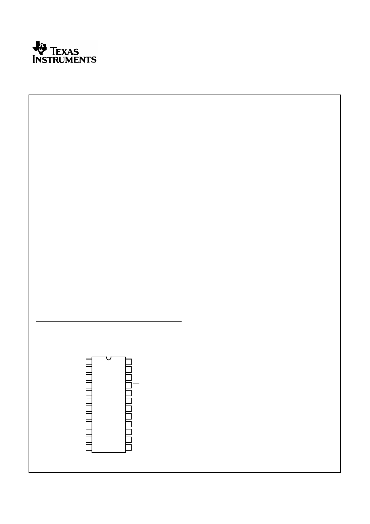
Pinout
CD74HC652, CD74HCT652
(PDIP, SOIC)
TOP VIEW
1
2
3
4
5
6
7
8
9
10
11
12
CAB
SAB
OE
AB
A0
A1
A2
A3
A4
A5
A6
A7
GND
16
17
18
19
20
21
22
23
24
15
14
13
V
CC
SBA
OE
BA
B0
B1
B3
B5
B6
B7
CBA
B2
B4
February 1998
CAUTION: These devices are sensitive to electrostatic discharge. Users should follow proper IC Handling Procedures.
Copyright
© Harris Corporation 1998
File Number 2229.2
CD74HC652,
CD74HCT652
High-Speed CMOS Logic
Octal-Bus Transceiver/Registers, Three-State
2
Description
The Harris CD74HC652 and CD74HCT652 three-state, octalbus transceiver/registers use silicon-gate CMOS technology
to achieve operating speeds similar to LSTTL with the low
power consumption of standard CMOS integrated circuits.
The CD74HC652 and CD74HCT652 have non-inverting
outputs. These devices consists of bus transceiver circuits, Dtype flip-flops, and control circuitry arranged for multiplexed
transmission of data directly from the data bus or from the
internal storage registers. Output Enables OE
AB
and OE
BA
are provided to control the transceiver functions. SAB and
SBA control pins are provided to select whether real-time or
stored data is transferred. The circuitry used for select control
will eliminate the typical decoding glitch that occurs in a
multiplexer during the transition between stored and real-time
data. A LOW input level selects real-time data, and a HIGH
selects stored data. The following examples demonstrates the
four fundamentals bus-management functions that can be
performed with the octal-bus transceivers and registers.
Data on the A or B data bus, or both, can be stored in the
internal D flip-flops by low-to-high transitions at the appropriate
clock pins (CAB or CBA) regardless of the select of the control
pins. When SAB and SBA are in the real-time transfer mode, it
is also possible to store data without using the D-type flip-flops
by simultaneously enabling OE
AB
and OEBA. In this
configuration, each output reinforces its input. Thus, when all
other data sources to the two sets of bus lines are at high
impedance, each set of bus lines will remain at its last state.
Ordering Information
PART NUMBER
TEMP. RANGE
(oC) PACKAGE
PKG.
NO.
CD74HC652EN -55 to 125 24 Ld PDIP E24.3
CD74HCT652M -55 to 125 24 Ld SOIC M24.3
NOTES:
1. When ordering, use the entire part number. Add the suffix 96 to
obtain the variant in the tape and reel.
2. Wafer and die is available which meets all electrical
specifications. Please contact your local sales office or Harris
customer service for ordering information.
CD74HC652, CD74HCT652CD74HC652, CD74HCT652
3
CD74HC652, CD74HCT652
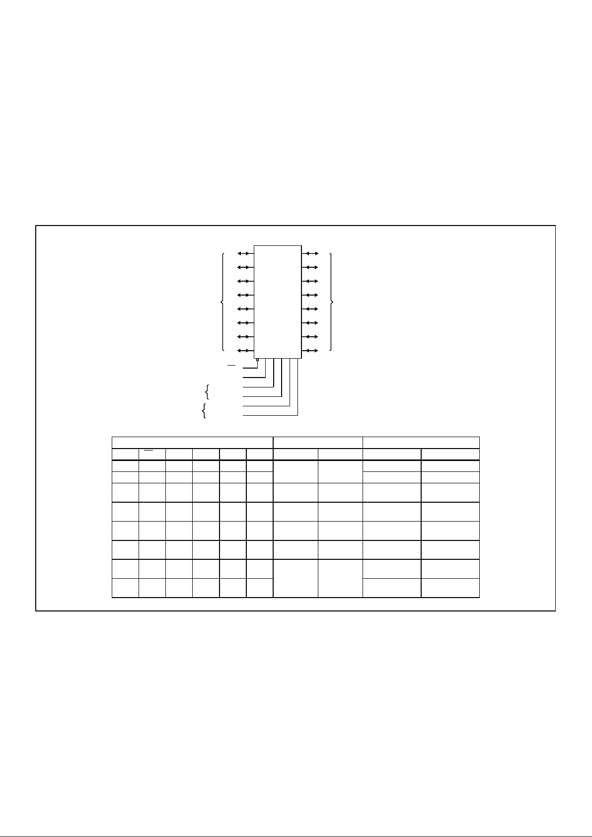
Functional Diagram
FUNCTION TABLE
INPUTS DATA I/O OPERATION OR FUNCTION
OE
AB
OE
BA
CAB CBA SAB SBA A0 THRU A7 B0 THRU B7 651 652
L H H or L H or L X X Input Input Isolation (Note 3) Isolation (Note 3)
LH↑↑X X Store A and B Data Store A and B Data
XH↑H or L X X Input Unspecified
(Note 4)
Store A, Hold B Store A, Hold B
HH↑↑X
(Note 5)
X Input Output Store A in Both
Registers
Store A in Both
Registers
L X H or L ↑ X X Unspecified
(Note 4)
Input Hold A, Store B Hold A, Store B
LL↑↑XX
(Note 5)
Output Input Store B in Both
Registers
Store B in Both
Registers
L L X X X L Output Input Real-Time B Data to
A Bus
Real-TimeBData to
A Bus
L L X H or L X H Stored B Data to A
Bus
Stored B Data to A
Bus
20
19
18
17
15
13
14
16
4
B0
B1
B2
B3
B4
B5
B6
B7
OE
BA
OE
AB
21
3
6
11
5
7
8
9
10
A0
A1
A2
A3
A4
A5
A6
A7
1
23
2
22
CAB CLOCK
CBA CLOCK
SAB SOURCE
SBA SOURCE
GND = PIN 12
V
CC
= PIN 24
B
DATA
PORT
A
DATA
PORT
FLIP-FLOP
CLOCKS
DATA
SOURCE
SELECTION
INPUTS

4
H H X X L X Input Output Real-Time A Data to
B Bus
Real-TimeA Datato
B Bus
H H H or L X H X Stored A Data to B
Bus
Stored A Data to B
Bus
H L H or L H or L H H Output Output Stored A Data to B
Bus and
Stored A Data to B
Bus
Stored B Data to A
Bus
Stored B Data to A
Bus
NOTES:
3. To prevent excess currents in the High-Z (isolation) modes, all I/O terminals should be terminated with 10kΩ to 1MΩ resistors.
4. The data output functions may be enabled or disabled by various signals at the OE
AB
or OEBAinputs. Data input functions are always
enabled; i.e., data at the bus pins will be stored on every low-to-high transition on the clock inputs.
5. Select Control = L: Clocks can occur simultaneously.
Select Control = H: Clocks must be staggered in order to load both registers.
FUNCTION TABLE
INPUTS DATA I/O OPERATION OR FUNCTION
OE
AB
OE
BA
CAB CBA SAB SBA A0 THRU A7 B0 THRU B7 651 652
CD74HC652, CD74HCT652CD74HC652, CD74HCT652

5
V
CC
OE
BA
GND
N
P
23
A
V
CC
GND
N
P
V
CC
CK
D
F/F
Q
21
3
OE
AB
2
SAB
22
SBA
1
CAB
CBA
B
20, (19, 18,
17, 16, 15,
14, 13)
4, (5, 6, 7, 8,
P
N
P
N
P
N
P
N
† Inverter not included in HC/HCT651
24 VCC12
GND
TO CHANNELS
2 THRU 8
F/F
ONE OF EIGHT IDENTICAL CHANNELS
†
†
9, 10, 11)
FIGURE 1. LOGIC BLOCK DIAGRAM
CD74HC652, CD74HCT652CD74HC652, CD74HCT652

6
Absolute Maximum Ratings
Thermal Information
DC Supply Voltage, V
CC
(Voltages Referenced to Ground) . . . . . . . . . . . . . . . . -0.5V to 7V
DC Input Diode Current, I
IK
For VI < -0.5V or VI > VCC + 0.5V. . . . . . . . . . . . . . . . . . . . . .±20mA
DC Drain Current, I
O
For -0.5V < VO < VCC + 0.5V. . . . . . . . . . . . . . . . . . . . . . . . . .±35mA
DC Output Diode Current, I
OK
For VO < -0.5V or VO > VCC + 0.5V . . . . . . . . . . . . . . . . . . . .±20mA
DC Output Source or Sink Current per Output Pin, I
O
For VO > -0.5V or VO < VCC + 0.5V . . . . . . . . . . . . . . . . . . . .±25mA
DC VCC or Ground Current, ICC . . . . . . . . . . . . . . . . . . . . . . . . .±50mA
Operating Conditions
Temperature Range, TA . . . . . . . . . . . . . . . . . . . . . . -55oC to 125oC
Supply Voltage Range, V
CC
HC Types . . . . . . . . . . . . . . . . . . . . . . . . . . . . . . . . . . . . .2V to 6V
HCT Types . . . . . . . . . . . . . . . . . . . . . . . . . . . . . . . . .4.5V to 5.5V
DC Input or Output Voltage, VI, VO . . . . . . . . . . . . . . . . . 0V to V
CC
Input Rise and Fall Time
2V . . . . . . . . . . . . . . . . . . . . . . . . . . . . . . . . . . . . . . 1000ns (Max)
4.5V. . . . . . . . . . . . . . . . . . . . . . . . . . . . . . . . . . . . . . 500ns (Max)
6V . . . . . . . . . . . . . . . . . . . . . . . . . . . . . . . . . . . . . . . 400ns (Max)
Thermal Resistance (Typical, Note 6) θJA (oC/W)
PDIP Package. . . . . . . . . . . . . . . . . . . . . . . . . . . . . 75
SOIC Package. . . . . . . . . . . . . . . . . . . . . . . . . . . . . 75
Maximum Junction Temperature (Hermetic Pac kage or Die) . . . 175oC
Maximum Junction Temperature (Plastic Package) . . . . . . . . 150oC
Maximum Storage Temperature Range . . . . . . . . . .-65oC to 150oC
Maximum Lead Temperature (Soldering 10s). . . . . . . . . . . . . 300oC
(SOIC - Lead Tips Only)
CAUTION: Stresses above those listed in “Absolute Maximum Ratings” may cause permanent damage to the device. This is a stress only rating and operation
of the device at these or any other conditions above those indicated in the operational sections of this specification is not implied.
NOTE:
6. θJA is measured with the component mounted on an evaluation PC board in free air.
DC Electrical Specifications
PARAMETER SYMBOL
TEST
CONDITIONS
VCC (V)
25
o
C -40oC TO 85oC -55oC TO 125oC
UNITSV
I
(V) VIS (V) MIN TYP MAX MIN MAX MIN MAX
HC TYPES
High Level Input
Voltage
V
IH
- - 2 1.5 - - 1.5 - 1.5 - V
4.5 3.15 - - 3.15 - 3.15 - V
6 4.2 - - 4.2 - 4.2 - V
Low Level Input
Voltage
V
IL
- - 2 - - 0.3 - 0.3 - 0.3 V
4.5 - - 0.9 - 0.9 - 0.9 V
6 - - 1.2 - 1.2 - 1.2 V
High Level Output
Voltage
CMOS Loads
V
OH
VIH or
V
IL
-0.02 2 1.9 - - 1.9 - 1.9 - V
-0.02 4.5 4.4 - - 4.4 - 4.4 - V
-0.02 6 5.9 - - 5.9 - 5.9 - V
High Level Output
Voltage
TTL Loads
---------V
-6 4.5 3.98 - - 3.84 - 3.7 - V
-7.8 6 5.48 - - 5.34 - 5.2 - V
Low Level Output
Voltage
CMOS Loads
V
OL
VIH or
V
IL
0.02 2 - - 0.1 - 0.1 - 0.1 V
0.02 4.5 - - 0.1 - 0.1 - 0.1 V
0.02 6 - - 0.1 - 0.1 - 0.1 V
Low Level Output
Voltage
TTL Loads
---------V
6 4.5 - - 0.26 - 0.33 - 0.4 V
7.8 6 - - 0.26 - 0.33 - 0.4 V
CD74HC652, CD74HCT652CD74HC652, CD74HCT652

7
Input Leakage
Current
I
I
VCC or
GND
-6--±0.1 - ±1-±1µA
Quiescent Device
Current
I
CC
VCC or
GND
0 6 - - 8 - 80 - 160 µA
Three- State Leakage
Current
V
IL
or VIHVO =
VCC or
GND
-6--±0.5 - ±5.0 - ±10 µA
HCT TYPES
High Level Input
Voltage
V
IH
- - 4.5 to
5.5
2-- 2 - 2 - V
Low Level Input
Voltage
V
IL
- - 4.5 to
5.5
- - 0.8 - 0.8 - 0.8 V
High Level Output
Voltage
CMOS Loads
V
OH
VIH or
V
IL
-0.02 4.5 4.4 - - 4.4 - 4.4 - V
High Level Output
Voltage
TTL Loads
-6 4.5 3.98 - - 3.84 - 3.7 - V
Low Level Output
Voltage
CMOS Loads
V
OL
VIH or
V
IL
0.02 4.5 - - 0.1 - 0.1 - 0.1 V
Low Level Output
Voltage
TTL Loads
6 4.5 - - 0.26 - 0.33 - 0.4 V
Input Leakage
Current
I
I
V
CC
and
GND
0 5.5 - ±0.1 - ±1-±1µA
Quiescent Device
Current
I
CC
VCC or
GND
0 5.5 - - 8 - 80 - 160 µA
Three- State Leakage
Current
V
IL
or VIHVO =
VCC or
GND
- 5.5 - - ±0.5 - ±5.0 - ±10 µA
Additional Quiescent
Device Current Per
Input Pin: 1 Unit Load
∆I
CC
V
CC
-2.1
- 4.5 to
5.5
- 100 360 - 450 - 490 µA
NOTE: For dual-supply systems theoretical worst case (V
I
= 2.4V, VCC = 5.5V) specification is 1.8mA.
DC Electrical Specifications (Continued)
PARAMETER SYMBOL
TEST
CONDITIONS
V
CC
(V)
25
o
C -40oC TO 85oC -55oC TO 125oC
UNITSV
I
(V) VIS (V) MIN TYP MAX MIN MAX MIN MAX
HCT Input Loading Table
INPUT UNIT LOADS
OE
BA
1.3
OE
AB
0.75
Clock A to B, B to A 0.6
Select A, Select B 0.45
Inputs A
0-A7
, B0-B
7
0.3
NOTE: Unit Load is ∆I
CC
limit specified in DC Electrical Specifica-
tions table, e.g., 360µA max at 25oC.
CD74HC652, CD74HCT652CD74HC652, CD74HCT652

8
Prerequisite for Switching Specifications
PARAMETER SYMBOL VCC(V)
25oC -40oC TO 85oC -55oC TO 125oC
UNITSMIN TYP MAX MIN TYP MAX MIN TYP MAX
HC TYPES
Maximum Clock
Frequency
f
MAX
2 6 - - 5 - - 4 - - MHz
4.5 30 - - 25 - - 20 - - MHz
6 35 - - 29 - - 23 - - MHz
Setup Time
Data to Clock
t
SU
260--75- -90--ns
4.5 12 - - 15 - - 18 - - ns
610--13- -15--ns
Hold Time
Data to Clock
t
H
235--45- -55--ns
4.5 7 - - 9 - - 11 - - ns
66--8--9--ns
Clock Pulse Width t
W
2 80 - - 100 - - 120 - - ns
4.5 16 - - 20 - - 24 - - ns
614--17- -20--ns
HCT TYPES
Maximum Clock
Frequency
f
MAX
4.5 25 - - 20 - - 17 - - MHz
Setup Time
Data to Clock
t
SU
4.5 12 - - 15 - - 18 - - ns
Hold Time
Data to Clock
t
H
4.5 5 - - 5 - - 5 - - ns
Clock Pulse Width t
W
4.5 25 - - 31 - - 38 - - ns
Switching Specifications Input t
r
, tf = 6ns
PARAMETER SYMBOL
TEST
CONDITIONS
V
CC
(V)
25
o
C -40oC TO 85oC -55oCTO125oC
UNITSMIN TYP MAX MIN MAX MIN MAX
HC TYPES
Propagation Delay,
Store A Data to B Bus
Store B Data to A Bus
t
PLH
, t
PHL
CL= 50pF 2 - - 220 - 275 - 300 ns
4.5 - - 44 - 55 - 66 ns
6 - - 37 - 47 - 5.6 ns
C
L
= 15pF 5 - 18 - ----ns
Propagation Delay,
A Data to B Bus
B Data to A Bus
t
PLH
, t
PHL
CL= 50pF 2 - - 135 - 170 - 205 ns
4.5 - - 27 - 34 - 41 ns
6 - - 23 - 29 - 35 ns
C
L
= 15pF 5 - 12 - ----ns
Propagation Delay,
Select to Data
t
PLH
, t
PHL
CL= 50pF 2 - - 170 - 215 - 255 ns
4.5 - - 34 - 43 - 51 ns
6 - - 29 - 37 - 43 ns
C
L
= 15pF 5 - 14 - ----ns
CD74HC652, CD74HCT652CD74HC652, CD74HCT652
9
Three-State Disabling Time Bus
to Output or Register to Output
t
PLZ
, t
PHZ
CL= 50pF 2 - - 175 - 220 - 265 ns
4.5 - - 35 - 44 - 53 ns
6 - - 30 - 37 - 45 ns
C
L
= 15pF 5 - 14 - ----ns
Three-State Enabling Time Bus
to Output or Register to Output
t
PZL
, t
PZH
CL= 50pF 2 - - 175 - 220 - 265 ns
4.5 - - 35 - 44 - 53 ns
6 - - 30 - 37 - 45 ns
C
L
= 15pF 5 - 14 - ----ns
Output Transition Time t
TLH
, t
THL
CL= 50pF 2 - - 60 - 75 - 90 ns
4.5 - - 12 - 15 - 18 ns
6 - - 10 - 13 - 15 ns
Three-State Output
Capacitance
C
O
- - - - 20 - 20 - 20 pF
Input Capacitance C
I
- - - - 10 - 10 - 10 pF
Maximum Frequency f
MAX
CL= 15pF 5 - 60 - ----MHz
Power Dissipation Capacitance
(Notes 7, 8)
C
PD
- 5-52-----pF
HCT TYPES
Propagation Delay,
Store A Data to B Bus
Store B Data to A Bus
t
PLH
, t
PHL
CL= 50pF 4.5 - - 44 - 55 - 66 ns
C
L
= 15pF 5 - 18 - ----ns
Propagation Delay,
A Data to B Bus
B Data to A Bus
t
PLH
, t
PHL
CL= 50pF 4.5 - - 37 - 46 - 56 ns
C
L
= 15pF 5 - 15 - ----ns
Propagation Delay,
Select to Data
t
PLH
, t
PHL
CL= 50pF 4.5 - - 46 - 58 - 69 ns
C
L
= 15pF 5 - 19 - ----ns
Three-State Disabling Time Bus
to Output or Register to Output
t
PLZ
, t
PHZ
CL= 50pF 4.5 - - 35 - 44 - 53 ns
C
L
= 15pF 5 - 14 - ----ns
Three-State Enabling Time Bus
to Output or Register to Output
t
PZL
, t
PZH
CL= 50pF 4.5 - - 45 - 56 - 68 ns
C
L
= 15pF 5 - 19 - ----ns
Output Transition Time t
TLH
, t
THL
CL= 50pF 4.5 - - 12 - 15 - 18 ns
Three-State Output
Capacitance
C
O
- - - - 20 - 20 - 20 pF
Input Capacitance C
I
- - - - 10 - 10 - 10 pF
Maximum Frequency f
MAX
CL= 15pF 5 - 45 - ----MHz
Power Dissipation Capacitance
(Notes 7, 8)
C
PD
- 5-52-----pF
NOTES:
7. C
PD
is used to determine the dynamic power consumption, per package.
8. PD = V
CC
2
CPD fi + Σ V
CC
2
CL fowhere fi = input frequency, fo = output frequency, CL = output load capacitance, CS = switch capaci-
tance, VCC = supply voltage.
Switching Specifications Input t
r
, tf = 6ns (Continued)
PARAMETER SYMBOL
TEST
CONDITIONS
V
CC
(V)
25
o
C -40oC TO 85oC -55oCTO125oC
UNITSMIN TYP MAX MIN MAX MIN MAX
CD74HC652, CD74HCT652

10
Test Circuits and Waveforms
NOTE: Outputs should be switching from 10% VCC to 90% VCC in
accordance with devicetruth table. For f
MAX
, input duty cycle = 50%.
FIGURE 2. HC CLOCK PULSE RISE AND FALL TIMES AND
PULSE WIDTH
NOTE: Outputs should be switching from 10% VCC to 90% VCC in
accordance with devicetruth table. For f
MAX
, input duty cycle = 50%.
FIGURE 3. HCT CLOCK PULSE RISE AND FALL TIMES AND
PULSE WIDTH
FIGURE 4. HC TRANSITION TIMES AND PROPAGATION
DELAY TIMES, COMBINATION LOGIC
FIGURE 5. HCT TRANSITION TIMES AND PROPAGATION
DELAY TIMES, COMBINATION LOGIC
CLOCK
90%
50%
10%
GND
V
CC
trC
L
tfC
L
50%
50%
t
WL
t
WH
10%
tWL+ tWH=
fC
L
I
CLOCK
2.7V
1.3V
0.3V
GND
3V
t
rCL
= 6ns
t
fCL
= 6ns
1.3V
1.3V
t
WL
t
WH
0.3V
t
WL
+ tWH=
fC
L
I
t
PHL
t
PLH
t
THL
t
TLH
90%
50%
10%
50%
10%
INVERTING
OUTPUT
INPUT
GND
V
CC
tr = 6ns tf = 6ns
90%
t
PHL
t
PLH
t
THL
t
TLH
2.7V
1.3V
0.3V
1.3V
10%
INVERTING
OUTPUT
INPUT
GND
3V
tr = 6ns
t
f
= 6ns
90%

11
FIGURE 6. HC SETUP TIMES, HOLD TIMES, REMOVAL TIME,
AND PROPAGATION DELAY TIMES FOR EDGE
TRIGGERED SEQUENTIAL LOGIC CIRCUITS
FIGURE 7. HCT SETUP TIMES, HOLD TIMES, REMOVAL TIME,
AND PROPAGATION DELAY TIMES FOR EDGE
TRIGGERED SEQUENTIAL LOGIC CIRCUITS
FIGURE 8. HC THREE-STATE PROPAGATION DELAY
WAVEFORM
FIGURE 9. HCT THREE-STATE PROPAGATION DELAY
WAVEFORM
NOTE: Opendrain waveforms t
PLZ
and t
PZL
are the same as those for three-state shown on the left. The test circuit is Output RL=1kΩto
VCC, CL = 50pF.
FIGURE 10. HC AND HCT THREE-STATE PROPAGATION DELAY TEST CIRCUIT
Test Circuits and Waveforms
(Continued)
trC
L
tfC
L
GND
V
CC
GND
V
CC
50%
90%
10%
GND
CLOCK
INPUT
DAT A
INPUT
OUTPUT
SET, RESET
OR PRESET
V
CC
50%
50%
90%
10%
50%
90%
t
REM
t
PLH
t
SU(H)
t
TLH
t
THL
t
H(L)
t
PHL
IC
C
L
50pF
t
SU(L)
t
H(H)
trC
L
tfC
L
GND
3V
GND
3V
1.3V
2.7V
0.3V
GND
CLOCK
INPUT
DAT A
INPUT
OUTPUT
SET, RESET
OR PRESET
3V
1.3V
1.3V
1.3V
90%
10%
1.3V
90%
t
REM
t
PLH
t
SU(H)
t
TLH
t
THL
t
H(L)
t
PHL
IC
C
L
50pF
t
SU(L)
1.3V
t
H(H)
1.3V
50%
10%
90%
GND
V
CC
10%
90%
50%
50%
OUTPUT
DISABLE
OUTPUT LOW
TO OFF
OUTPUT HIGH
TO OFF
OUTPUTS
ENABLED
OUTPUTS
DISABLED
OUTPUTS
ENABLED
6ns 6ns
t
PZH
t
PHZ
t
PZL
t
PLZ
0.3
2.7
GND
3V
10%
90%
1.3V
1.3V
OUTPUT
DISABLE
OUTPUT LOW
TO OFF
OUTPUT HIGH
TO OFF
OUTPUTS
ENABLED
OUTPUTS
DISABLED
OUTPUTS
ENABLED
t
r
6ns
t
PZH
t
PHZ
t
PZL
t
PLZ
6ns t
f
1.3
IC WITH
THREE-
STATE
OUTPUT
OTHER
INPUTS
TIED HIGH
OR LOW
OUTPUT
DISABLE
VCC FOR t
PLZ
AND t
PZL
GND FOR t
PHZ
AND t
PZH
OUTPUT
R
L
= 1kΩ
C
L
50pF

IMPORTANT NOTICE
T exas Instruments and its subsidiaries (TI) reserve the right to make changes to their products or to discontinue
any product or service without notice, and advise customers to obtain the latest version of relevant information
to verify, before placing orders, that information being relied on is current and complete. All products are sold
subject to the terms and conditions of sale supplied at the time of order acknowledgement, including those
pertaining to warranty, patent infringement, and limitation of liability.
TI warrants performance of its semiconductor products to the specifications applicable at the time of sale in
accordance with TI’s standard warranty. Testing and other quality control techniques are utilized to the extent
TI deems necessary to support this warranty. Specific testing of all parameters of each device is not necessarily
performed, except those mandated by government requirements.
CERT AIN APPLICATIONS USING SEMICONDUCTOR PRODUCTS MAY INVOLVE POTENTIAL RISKS OF
DEATH, PERSONAL INJURY, OR SEVERE PROPERTY OR ENVIRONMENTAL DAMAGE (“CRITICAL
APPLICATIONS”). TI SEMICONDUCTOR PRODUCTS ARE NOT DESIGNED, AUTHORIZED, OR
WARRANTED TO BE SUITABLE FOR USE IN LIFE-SUPPORT DEVICES OR SYSTEMS OR OTHER
CRITICAL APPLICATIONS. INCLUSION OF TI PRODUCTS IN SUCH APPLICA TIONS IS UNDERST OOD TO
BE FULLY AT THE CUSTOMER’S RISK.
In order to minimize risks associated with the customer’s applications, adequate design and operating
safeguards must be provided by the customer to minimize inherent or procedural hazards.
TI assumes no liability for applications assistance or customer product design. TI does not warrant or represent
that any license, either express or implied, is granted under any patent right, copyright, mask work right, or other
intellectual property right of TI covering or relating to any combination, machine, or process in which such
semiconductor products or services might be or are used. TI’s publication of information regarding any third
party’s products or services does not constitute TI’s approval, warranty or endorsement thereof.
Copyright 1999, Texas Instruments Incorporated
 Loading...