


Richtek RT9284A-15PJ6, RT9284A-15PJ6E, RT9284A-20GJ6E, RT9284A-20PJ6, RT9284A-20PJ6E Schematic [ru]
...RT9284A/B
Tiny Package, High Performance, Constant Current Switching Regulator for White LED
General Description
The RT9284A/B is a compact, high efficient and high integration LED driver. Internal 22V MOSFET can support 2 to 5 White LEDs for backlighting and camera flashing.
Highly integration and internal compensation network minimizes as 5 external component counts. Optimized operation frequency can meet the requirement of small LC filters value and low operation current with high efficiency. Internal soft start function can reduce the inrush current. Tiny package type of TSOT-23-5 and TSOT-23-6 packages provide the best solution for PCB space saving and total BOM cost.
Features
zVIN Operating Range : 2.7V to 5.5V
zMaximum Output Voltage up to 20V
zDimming with Zero-inrush and Wide Frequency Range of 100 to 100kHz
zOver Voltage Protection
zOutput Current up to 100mA at VOUT : 12V
zZero Shutdown Supply Current
zMinimize the External Component
zSmall LC Filter
zInternal Soft Start
zRoHS Compliant and 100% Lead (Pb)-Free
Ordering Information
RT9284
 (-
(-

 )
)

Package Type
J5 : TSOT-23-5
J6 : TSOT-23-6
Lead Plating System
P : Pb Free
G : Green (Halogen Free and Pb Free)
OVP Voltage 15 : 15V
20 : 20V
FB Voltage
A : 1.235V
B : 0.25V
Note :
Richtek products are :
`RoHS compliant and compatible with the current requirements of IPC/JEDEC J-STD-020.
`Suitable for use in SnPb or Pb-free soldering processes.
Marking Information
For marking information, contact our sales representative directly or through a Richtek distributor located in your area.
Applications
zCamera Flash White LED
zMobile Phone, Smart Phone LED Backlight
zPDA LED Backlight
zDigital Still Camera
zCamcorder
Pin Configurations
TOP VIEW
VDD EN
5 4
2 3
LX GND FB
TSOT-23-5
VDD OVP EN
6 5 4
2 3
LX GND FB
TSOT-23-6
DS9284A/B-07 April 2011 |
www.richtek.com |
|
1 |

RT9284A/B
Typical Application Circuit
|
|
|
L1 |
|
D1 |
OVP |
|
|
|
|
4.7uH to 22uH |
SS0520 |
15V |
|
|
|
|
|
|
|
|
|
|
VIN + |
C1 |
|
|
|
|
C2 |
ILED |
2.7V to 5.5V |
1uF |
|
RT9284 |
|
1uF/16V |
|
|
|
6 |
1 |
|
|
|||
|
|
|
|
||||
|
|
VDD |
LX |
|
|
||
Dimming |
|
4 EN |
OVP 5 |
|
|
||
Control |
|
2 GND |
|
|
|
|
|
100Hz-100kHz |
FB 3 |
|
|
||||
|
|
|
|
|
|
|
R1 |
Figure 1. Application for Driving 3 Series WLEDs
|
|
|
|
L1 |
D1 |
|
|
OVP |
|
|
|
|
|
4.7uH to 22uH |
SS0520 |
|
|
18V |
|
|
|
|
|
|
|
|
|
|
|
|
|
|
VIN + |
C1 |
|
|
|
|
|
|
C2 |
ILED |
|
2.7V to 5.5V |
1uF |
|
RT9284 |
|
|
R2 |
1uF/25V |
|
|
|
|
|
|
|
|
|
|
||||
|
|
|
6 VDD |
LX |
1 |
|
600k |
|
|
|
Dimming |
|
|
4 EN |
OVP |
5 |
|
|
|
|
|
Control |
|
|
2 GND |
|
OVP 15V |
|
|
|
|
|
100Hz-100kHz |
|
FB 3 |
|
|
|
|
|
|||
|
|
|
|
|
|
|
|
|
R1 |
|
Figure 2. Application for Driving 4 Series WLEDs |
|
|
||||||||
|
|
|
|
L1 |
D1 |
|
OVP |
|
|
|
|
|
|
4.7uH to 22uH |
SS0520 |
20V |
|
|
|||
|
|
|
|
|
|
|
|
|
||
VIN + |
C1 |
|
|
|
|
|
|
C2 |
ILED |
|
2.7V to 5.5V |
1uF |
|
RT9284B |
|
|
|
1uF/25V |
|
|
|
|
6 |
|
|
|
|
|
|
|||
|
|
VDD |
LX 1 |
|
|
|
|
|
|
|
Dimming |
|
4 EN |
OVP 5 |
|
|
|
|
|
|
|
Control |
|
2 GND |
|
|
|
|
|
|
|
|
100Hz-100kHz |
FB 3 |
VFB = 0.25V |
|
|
|
|
||||
|
|
|
|
|
|
|
R1 |
|
||
Figure 3. Application for Driving 5 Series WLEDs |
|
|
||||||||
|
|
|
L1 |
D1 |
OVP |
|
V |
|
||
|
|
|
4.7uH to 22uH |
SS0520 |
15V |
|
OUT |
|||
VIN + |
|
|
|
|
|
|
|
|
12V |
|
C1 |
|
|
|
|
|
|
R1 |
C2 |
|
|
2.7V to 5.5V |
1uF |
|
RT9284A |
|
|
|
1uF/16V |
|||
|
6 |
|
|
|
130k |
|
|
|||
|
|
VDD |
LX 1 |
|
|
|
|
|
|
|
|
|
4 EN |
OVP 5 |
|
|
|
|
|
|
|
|
|
2 GND |
FB 3 |
|
|
|
VFB = 1.235V |
|
||
|
|
|
|
|
|
|
|
R2 |
|
|
|
|
|
|
|
|
|
|
15k |
|
|
Figure 4. Application for Constant Output Voltage |
|
|
||||||||
www.richtek.com |
|
|
|
|
|
|
|
|
DS9284A/B-07 April 2011 |
|
2 |
|
|
|
|
|
|
|
|
|
|
RT9284A/B
Pin Description
|
Pin No. |
Pin Name |
Pin Function |
||
|
|
|
|||
TSOT-23-5 |
TSOT-23-6 |
||||
|
|
||||
|
|
|
|
|
|
1 |
|
1 |
LX |
Switch Pin. Connect this Pin to inductor and catch diode. Minimize the track |
|
|
area to reduce EMI. |
||||
|
|
|
|
||
2 |
|
2 |
GND |
Ground Pin |
|
|
|
|
|
|
|
|
|
|
|
Feedback Reference Voltage Pin. Series connect a resistor between WLED |
|
3 |
|
3 |
FB |
and ground as a current sense. Sense the current feedback voltage to set |
|
|
|
|
|
the current rating. |
|
|
|
|
|
Chip Enable (Active High). Voltage sensing input to trigger the function of |
|
4 |
|
4 |
EN |
over voltage protection. Note that this pin is high impedance. There should |
|
|
be a pull low 100kΩ resistor connected to GND when the control signal is |
||||
|
|
|
|
||
|
|
|
|
floating. |
|
-- |
|
5 |
OVP |
Over Voltage Protection Pin. Voltage sensing input to trigger the function of |
|
|
over voltage protection. Leave it unconnected to disable this function. |
||||
|
|
|
|
||
5 |
|
6 |
VDD |
Supply Input Voltage Pin. Bypass 1uF capacitor to GND to reduce the input |
|
|
noise. |
||||
|
|
|
|
||
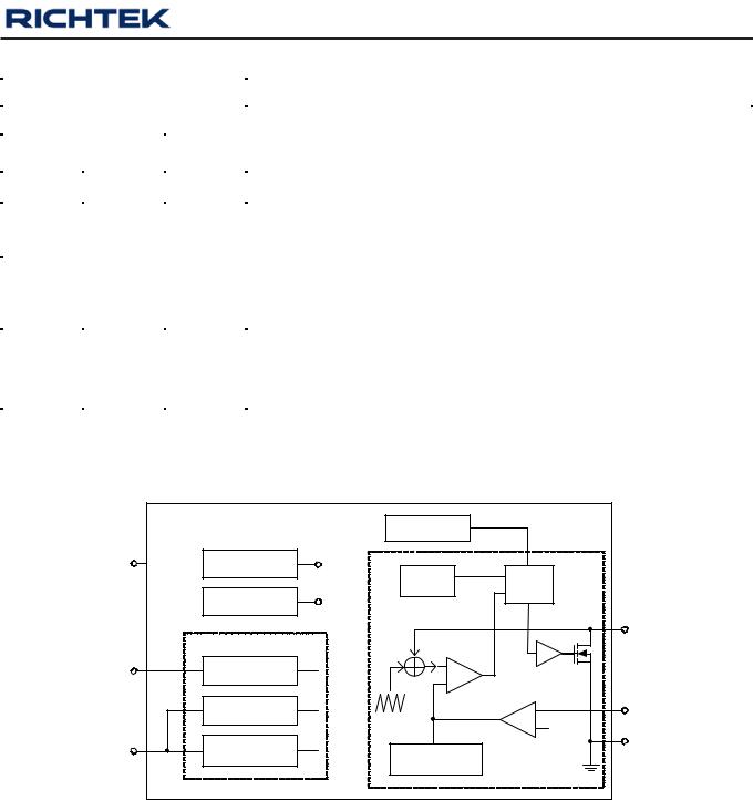
Function Block Diagram
|
|
|
1.2MHz OSC |
|
|
|
VDD |
Current Bias |
ibias |
OCP |
PWM |
|
|
|
|
|
|
|
||
|
BandGap |
VREF |
750mA |
Logic |
|
|
|
|
|
|
|
||
|
Protection Circuit |
|
|
|
|
LX |
|
|
|
|
|
|
|
OVP |
OVP |
|
+ |
Buffer |
|
|
|
|
|
- |
|
|
|
|
UVLO |
|
|
+ |
|
FB |
|
Timer |
|
|
- |
VREF |
GND |
EN |
|
|
|
|
||
5ms |
|
Soft Start |
|
|
|
|
|
|
|
|
|
DS9284A/B-07 April 2011 |
www.richtek.com |
|
3 |

RT9284A/B
Absolute Maximum Ratings |
(Note 1) |
|
|
|
|
|
|
||||
z Supply Input Voltage ---------------------------------------------------------------------------------------------------- |
|
|
|
|
|
|
−0.3V to 7V |
||||
z LX Input Voltage ---------------------------------------------------------------------------------------------------------- |
|
|
|
|
|
|
|
−0.3V to 22V |
|||
z OVP Voltage -------------------------------------------------------------------------------------------------------------- |
|
|
|
|
|
|
|
−0.3V to 22V |
|||
z The Other Pins ----------------------------------------------------------------------------------------------------------- |
|
|
|
|
|
|
|
−0.3V to 6V |
|||
z Power Dissipation, PD @ TA = 25°C |
|
|
|
|
|
|
|
|
|||
TSOT-23-5 ----------------------------------------------------------------------------------------------------------------- |
|
|
|
|
|
|
|
0.455W |
|||
TSOT-23-6 ----------------------------------------------------------------------------------------------------------------- |
|
|
|
|
|
|
|
0.455W |
|||
z Package Thermal Resistance |
(Note 2) |
|
|
|
|
|
|
|
|
||
TSOT-23-5, θJA ------------------------------------------------------------------------------------------------------------ |
|
|
|
|
|
|
|
220°C/W |
|||
TSOT-23-6, θJA ------------------------------------------------------------------------------------------------------------ |
|
|
|
|
|
|
|
220°C/W |
|||
z Lead Temperature (Soldering, 10 sec.) ----------------------------------------------------------------------------- |
|
|
|
|
260°C |
|
|
|
|||
z Junction Temperature --------------------------------------------------------------------------------------------------- |
|
|
|
|
|
|
150°C |
|
|
|
|
z Storage Temperature Range ------------------------------------------------------------------------------------------- |
|
|
|
|
|
|
−65°C to 150°C |
||||
z ESD Susceptibility |
(Note 3) |
|
|
|
|
|
|
|
|
|
|
HBM (Human Body Mode) --------------------------------------------------------------------------------------------- |
|
|
|
|
|
|
2kV |
|
|
|
|
MM (Machine Mode) ---------------------------------------------------------------------------------------------------- |
|
|
|
|
|
|
200V |
|
|
|
|
Recommended Operating Conditions (Note 4) |
|
|
|
|
|
|
|||||
z Supply Input Voltage ---------------------------------------------------------------------------------------------------- |
|
|
|
|
|
|
2.7V to 5.5V |
||||
z Junction Temperature Range ------------------------------------------------------------------------------------------ |
|
|
|
|
|
|
−40°C to 125°C |
||||
z Ambient Temperature Range ------------------------------------------------------------------------------------------ |
|
|
|
|
|
|
−40°C to 85°C |
||||
Electrical Characteristics |
|
|
|
|
|
|
|
|
|||
(VIN = 3.7V, TA = 25°C unless otherwise specified) |
|
|
|
|
|
|
|||||
Parameter |
|
Symbol |
|
Test Conditions |
Min |
Typ |
Max |
|
Unit |
|
|
|
|
|
|
|
|
|
|
|
|
|
|
System Supply Input |
|
|
|
|
|
|
|
|
|
|
|
|
|
|
|
|
|
|
|
|
|
|
|
Operation voltage Range |
|
VDD |
|
|
2.7 |
-- |
5.5 |
|
V |
|
|
Under Voltage Lock Out |
|
VDD |
|
|
1.8 |
2.2 |
2.5 |
|
V |
|
|
Quiescent Current |
|
|
IDD |
|
FB = 1.5V, No switch |
50 |
300 |
1000 |
|
uA |
|
Supply Current |
|
|
IDD |
|
FB = 0V, Switch |
0.1 |
2 |
3 |
|
mA |
|
Shut Down Current |
|
|
IDD |
|
VEN < 0.4V |
-- |
-- |
1 |
|
uA |
|
Line Regulation |
|
|
|
|
VIN : 3.0~4.3V |
-- |
3 |
-- |
|
% |
|
Oscillator |
|
|
|
|
|
|
|
|
|
|
|
|
|
|
|
|
|
|
|
|
|
|
|
Operation Frequency |
|
|
fOSC |
|
|
0.9 |
1.2 |
1.5 |
|
MHz |
|
Maximum Duty Cycle |
|
|
|
|
|
85 |
-- |
-- |
|
% |
|
|
|
|
|
|
|
|
|
|
|
|
|
Dimming Frequency |
|
|
|
|
|
100 |
-- |
100k |
|
Hz |
|
|
|
|
|
|
|
|
|
|
|
|
|
Reference Voltage |
|
|
|
|
|
|
|
|
|
|
|
|
|
|
|
|
|
|
|
|
|
|
|
Feedback Voltage |
(Note 5) |
|
RT9284A |
|
|
1.173 |
1.235 |
1.296 |
|
V |
|
|
|
|
|
|
|
|
|
|
|||
|
RT9284B |
|
|
0.237 |
0.25 |
0.263 |
|
|
|||
|
|
|
|
|
|
|
|
||||
|
|
|
|
|
|
|
|
|
|
|
|
|
|
|
|
|
|
|
|
To be continued |
|||
|
|
|
|
|
|
|
|
|
|
|
|
www.richtek.com |
|
|
|
|
|
|
DS9284A/B-07 |
April 2011 |
|||
4 |
|
|
|
|
|
|
|
|
|
|
|

RT9284A/B
Parameter |
Symbol |
Test Condition |
Min |
Typ |
Max |
Unit |
|
MOSFET |
|
|
|
|
|
|
|
|
|
|
|
|
|
|
|
On Resistance of MOSFET |
RDS(ON) |
|
-- |
0.75 |
-- |
Ω |
|
Protection |
|
|
|
|
|
|
|
|
|
|
|
|
|
|
|
OVP Threshold |
VOVP |
for 2,3,4 WLEDs application |
14 |
15 |
16 |
V |
|
|
|
|
|
||||
for 5 WLED application |
19 |
20 |
21 |
||||
|
|
|
|||||
|
|
|
|
|
|
|
|
OVP Sink Current |
|
|
-- |
5 |
-- |
μA |
|
|
|
|
|
|
|
|
|
OCP |
|
|
-- |
750 |
-- |
mA |
|
|
|
|
|
|
|
|
|
Shut Down Voltage |
VEN |
|
-- |
-- |
0.4 |
V |
|
Enable Voltage |
VEN |
|
1.5 |
-- |
-- |
V |
Note 1. Stresses listed as the above “Absolute Maximum Ratings” may cause permanent damage to the device. These are for stress ratings. Functional operation of the device at these or any other conditions beyond those indicated in the operational sections of the specifications is not implied. Exposure to absolute maximum rating conditions for extended periods may remain possibility to affect device reliability.
Note 2. θJA is measured in the natural convection at TA = 25°C on a low effective thermal conductivity test board of JEDEC 51-3 thermal measurement standard.
Note 3. Devices are ESD sensitive. Handling precaution recommended.
Note 4. The device is not guaranteed to function outside its operating conditions. Note 5. Floating the OVP pin to disable OVP function.
DS9284A/B-07 April 2011 |
www.richtek.com |
|
5 |
 Loading...