


Richtek RT9261-27GX, RT9261-27PX, RT9261-28PB, RT9261-30GB, RT9261-30PB Schematic [ru]
...
|
RT9261/A |
|
VFM Step-Up DC/DC Converter |
|
|
General Description |
Features |
|
The RT9261 Series are VFM Step-upDC/DC ICs with ultra |
z Minimal Number of External Components ( Only |
|
low supply current by CMOS process and suitable for |
an Inductor, a Diode, and a Capacitor) |
|
use with battery-powered instruments. |
z Ultra Low Input Current ( 5μA at Switch Off) |
|
The RT9261 IC consists of an oscillator, a VFM control |
z ±2% High Output Voltage Accuracy |
|
z Low Ripple and Low Noise |
||
circuit, a driver transistor (LX switch), a reference voltage |
||
z Low Start-up Voltage, 0.85V at 1mA |
||
unit, an error amplifier, resistors for voltage detection, and |
||
z 75% Efficiency with Low Cost Inductor |
||
a LX switch protection circuit. A low ripple and high |
||
z +50 ppm/ °C Low Temperature-Drift |
||
efficiency step-up DC/DC converter can be constructed of |
||
z SOT-89 and SOT-23-5 Small Packages |
||
this RT9261 IC with only three external components. |
||
z RoHS Compliant and 100% Lead (Pb)-Free |
||
The RT9261A IC provides with a drive pin (EXT) for an |
||
Applications |
||
external transistor, so that a power transistor can be |
||
externally applied. Therefore, the RT9261A IC is |
z Power source for battery-powered equipment |
|
recommended for applications where large currents are |
||
z Power source for cameras, camcorders, VCRs, PDAs, |
||
required. EN pin enables circuit to set the standby supply |
||
pagers, electronic data banks, and hand-held |
||
current at a maximum of 0.5μA. |
||
communication equipment |
||
|
||
Ordering Information |
z Power source for applications, which require higher |
|
voltage than that of batteries used in the appliances |
||
RT9261/A- |
||
|
Package Type |
Pin Configurations |
|
|
||||
B : SOT-23-5 |
|
|
|||||
X : SOT-89 |
|
|
|
(TOP VIEW) |
|
|
|
Lead Plating System |
|
|
|
|
|
||
|
|
|
|
|
|
||
P : Pb Free |
|
|
|
|
|
|
|
G : Green (Halogen Free and Pb Free) |
|
|
|
|
|
|
|
Output Voltage |
|
|
|
|
|
|
|
15 |
: 1.5V |
1 |
2 |
3 |
1 |
2 |
3 |
16 |
: 1.6V |
|
|
|
|
|
|
|
: |
GND VOUT |
LX |
GND VOUT EXT |
|||
49 |
: 4.9V |
||||||
50 |
: 5.0V |
|
(TAB) |
|
|
(TAB) |
|
|
RT9261 |
|
|
RT9261A |
|
||
Use external switch |
|
|
|
|
|||
|
|
|
SOT-89 |
|
|
||
Use internal switch |
|
|
|
|
|
||
Note : |
|
|
|
|
|
|
|
|
|
|
|
|
|
|
|
|
|
Richtek products are : |
LX |
GND |
|
EXT |
GND |
||||||||||||
` RoHS compliant and compatible with the current require- |
|
||||||||||||||||
|
|
|
|
|
|
|
|
|
|
|
|
|
|
|
|
|
|
|
|
|
|
|
|
|
|
|
|
|
|
|
|
|
|
|
|
ments of IPC/JEDEC J-STD-020. |
5 |
|
|
|
4 |
|
|
5 |
|
|
4 |
|
|
||||
|
|
|
|
|
|
|
|
|
|
|
|
|
|
|
|
|
|
` Suitable for use in SnPb or Pb-free soldering processes. |
|
|
2 |
3 |
|
|
2 |
3 |
|
|
|||||||
|
|
|
|
|
|
|
|
|
|
|
|
|
|
|
|
|
|
Marking Information |
EN VOUT NC |
|
EN VOUT NC |
||||||||||||||
|
|
RT9261 |
|
|
RT9261A |
||||||||||||
For marking information, contact our sales representative |
|
|
|
|
|
|
|
|
SOT-23-5 |
|
|
|
|
||||
directly or through a Richtek distributor located in your |
|
|
|
|
|
|
|
|
|
|
|
|
|||||
|
|
|
|
|
|
|
|
|
|
|
|
|
|
|
|
|
|
area. |
|
|
|
|
|
|
|
|
|
|
|
|
|
|
|
|
|
|
|
|
|
|
|
|
|
|
|
|
|
|
|
|
|
|
|
DS9261/A-16 April 2011 |
|
|
|
|
|
|
|
|
|
|
|
www.richtek.com |
|||||
|
|
|
|
|
|
|
|
|
|
|
|
|
|
1 |
|||

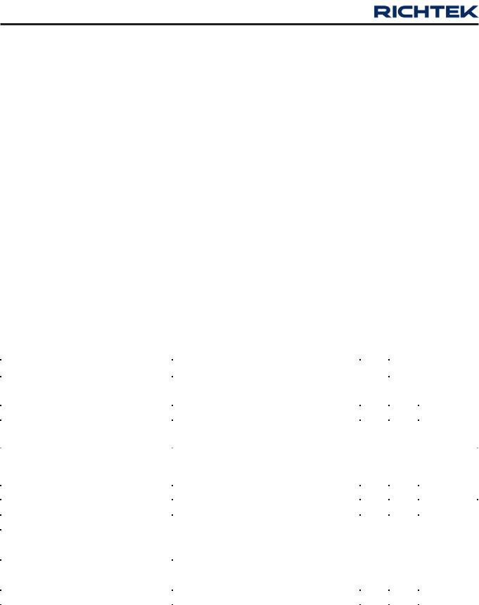
RT9261/A
Typical Application Circuit
|
|
D1 |
|
|
|
1N5819 |
|
L1 |
|
RT9261xX |
|
100µH |
LX |
VOUT |
VOUT |
|
GND |
+ |
|
VIN |
|
COUT |
|
|
|
22µF |
|
|
|
|
Figure 1
|
|
D1 |
|
|
|
1N5819 |
|
L1 |
RT9261xB |
|
|
100µH |
LX |
VOUT |
VOUT |
|
|
+ |
|
VIN |
NC |
|
COUT |
|
22µF |
||
|
|
||
|
EN |
GND |
|
|
|
||
|
|
|
|
L1 |
|
|
D1 |
|
|
|
|
|
|
27µH |
|
|
1N5819 |
|
|
Cb |
|
|
|
|
RT9261AxX |
|
||
0.01µF |
|
|||
VIN |
|
EXT |
VOUT |
VOUT |
ZTX |
|
|
GND |
+ |
|
|
COUT |
||
650 Tr |
Rb |
|
|
22µF |
|
300 |
|
|
|
Figure 2
L1 |
|
|
D1 |
|
|
|
|
|
|
|
|
27µH |
|
|
1N5819 |
|
|
|
|
|
|
|
|
VIN |
|
NC |
RT9261AxB |
|
|
|
Cb |
VOUT |
+ |
VOUT |
|
|
0.01µF |
EXT |
|
COUT |
|
ZTX |
|
|
|
22µF |
|
|
|
EN GND |
|
||
|
|
|
|
||
650 |
Tr |
Rb |
|
|
|
|
|
|
|||
|
|
300 |
|
|
|
Figure 3 |
Figure 4 |
|
|
|
D1 |
|
|
|
|
1N5819 |
|
|
L1 |
RT9261xB |
VOUT |
|
|
27µH |
LX |
VOUT |
|
|
|
|
+ |
|
VIN |
NC |
|
|
COUT |
|
|
22µF |
||
|
|
|
||
|
Chip |
EN |
|
|
|
GND |
|
||
|
Enable |
|
|
|
Figure 5
www.richtek.com |
DS9261/A-16 April 2011 |
2 |
|
|
|
|
|
|
|
RT9261/A |
Functional Pin Description |
|
|
|
|
||
|
Pin No. |
|
|
Pin Name |
Pin Function |
|
RT9261-□□□X |
RT9261A-□□□X |
RT9261-□□□B |
RT9261A-□□□B |
|||
|
|
|
|
|
|
|
1 |
1 |
|
4 |
4 |
GND |
Ground. |
|
|
|
|
|
|
|
2 |
2 |
|
2 |
2 |
VOUT |
Output Voltage. |
3 |
-- |
|
5 |
-- |
LX |
Pin for Switching. |
|
|
|
|
|
|
|
-- |
3 |
|
-- |
5 |
EXT |
Drive External Device. |
|
|
|
|
|
|
|
-- |
-- |
|
1 |
1 |
EN |
Chip Enable (Active High). |
|
|
|
|
|
|
|
-- |
-- |
|
3 |
3 |
NC |
No Internal Connected. |
|
|
|
|
|
|
|
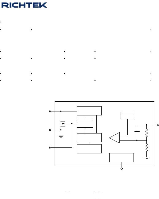
Function Block Diagram
LX |
|
VLX Limiter |
|
|
|
|
VREF |
|
LXSW |
Buffer |
VOUT |
|
|
||
|
|
|
|
GND |
|
|
|
|
|
VFM Control |
- |
|
|
+ |
|
|
|
|
|
EXT |
|
|
Error |
|
OSC 100kHz |
Amplifier |
|
|
|
|
Chip Enable |
|
|
|
EN |
Notes:
(1)LX Pin...... only for 9261- 

 xX and 9261-
 xB
xB
(2)EXT Pin.... only for 9261A- 
 xX and 9261A-
 xB
xB
(3)EN Pin...... only for 9261- 

 xB and 9261A-
 xB
xB
DS9261/A-16 April 2011 |
www.richtek.com |
3
RT9261/A
Absolute Maximum Ratings
z Output Voltage ------------------------------------------------------------------------------------------------------ |
8V |
z LX Pin Voltage (1) ------------------------------------------------------------------------------------ |
8V |
z EXT Pin Voltage (2) ------------------------------------------------------------------------------------------------- |
−0.3 to VOUT +0.3V |
z EN Pin Voltage (3) --------------------------------------------------------------------------------------------------- |
−0.3 to VOUT +0.3V |
z LX Pin Output Current (1) ------------------------------------------------------------------------------------------ |
250mA |
z EXT Pin Current (2) -------------------------------------------------------------------------------------------------- |
±50mA |
z Power Dissipation, PD @ TA = 25°C |
|
SOT-89 ---------------------------------------------------------------------------------------------------------------- |
0.5W |
SOT-23-5-------------------------------------------------------------------------------------------------------------- |
0.25W |
z Package Thermal Resistance |
|
SOT-89, θJC ---------------------------------------------------------------------------------------------------------- |
100°C/W |
SOT-89, θJA ---------------------------------------------------------------------------------------------------------- |
300°C/W |
SOT-23-5, θJA -------------------------------------------------------------------------------------------------------- |
250°C/W |
z Operating Temperature Range ----------------------------------------------------------------------------------- |
−20 to +85°C |
z Storage Temperature Range -------------------------------------------------------------------------------------- |
165°C |
z Lead Temperature (Soldering, 10 sec.) ------------------------------------------------------------------------ |
260°C |
Notes: |
|
(1)Applicable to RT9261- 
 xX and RT9261-
 xB
xB
(2)Applicable to RT9261A- 
 xX and RT9261A-
 xB
xB
(3)Applicable to RT9261- 
 xB and RT9261A-
 xB
xB
Electrical Characteristics (Refer to Figure 1)
Parameter |
Symbol |
Test Conditions |
|
|
Min |
Typ |
Max |
Unit |
||
|
|
|
|
|
|
|
|
|
|
|
Output Voltage Accuracy |
VOUT |
|
|
|
|
|
−2 |
-- |
2 |
% |
Input Voltage |
VIN |
|
|
|
|
|
-- |
-- |
7 |
V |
Start-up Voltage |
VST |
IOUT = 1mA, VIN: 0 → 2V |
|
|
|
-- |
0.85 |
1 |
V |
|
Hold-on Voltage |
VHO |
IOUT = 1mA, VIN: 2 → 0V |
|
|
|
0.7 |
-- |
-- |
V |
|
|
|
|
V |
≤ 3.5V (1) |
|
|
-- |
15 |
18 |
|
Input Current 1 |
|
VIN at no load |
OUT |
|
|
|
|
|
|
μA |
|
3.5V < VOUT ≤ |
5V |
(2) |
-- |
18 |
24 |
||||
|
|
|
|
|
||||||
Input Current 2 |
|
VOUT in switch off condition |
|
|
-- |
5 |
8 |
μA |
||
|
|
|
|
|
|
|
|
|
|
|
LX Switching Current |
ISWITCHING |
VLX = 0.4V |
VOUT ≤ 3.5V (1) |
|
|
60 |
-- |
-- |
mA |
|
3.5V < VOUT ≤ 5V (2) |
80 |
-- |
-- |
|||||||
LX Leakage Current |
ILEAKAGE |
VLX = 6V |
|
|
|
|
-- |
-- |
0.5 |
μA |
Maximum Oscillator |
FMAX |
|
|
|
|
|
80 |
120 |
160 |
kHz |
Oscillator Duty Cycle |
D |
On ( V ” L ” ) side |
VOUT = 2.5V to 5V |
65 |
75 |
85 |
% |
|||
|
|
|
|
|
|
|
|
|||
|
OSC |
LX |
VOUT = 1.5V to 2.4V |
60 |
70 |
80 |
% |
|||
|
|
|
||||||||
Efficiency |
|
|
|
|
|
|
-- |
75 |
-- |
% |
VLX Voltage Limit |
|
LX switch on |
|
|
|
|
0.65 |
0.8 |
1 |
V |
Notes:
(1)Unless otherwise provided, VIN = 1.8V, VSS = 0V, IOUT = 10mA, TOPT = 25°C, and External Circuit of Typical Application (2)Unless otherwise provided, VIN = 3V, VSS = 0V, IOUT = 10mA, TOPT = 25°C, and External Circuit of Typical Application
www.richtek.com |
DS9261/A-16 April 2011 |
4 |
|
 Loading...