


43V 4-CH LED Driver
RT8510
General Description
The RT8510 is a high efficiency driver for white LEDs. It is
designed for LCD panels that employ a n array of LEDs a s
the lighting source. An integrated switch current mode
boost controller drives four strings in parallel and supports
up to 12 pieces of LED per string. The internal current
sinks support a maximum of ±2% current mismatching
for excellent brightness uniformity in ea ch string of LED.
To provide enough headroom for current sink operation
the boost controller monitors the minimum voltage of
feedback pins a nd regulates a n optimized output voltage
for power efficiency .
The RT8510 ha s a wide input voltage ra nge from 4.2V to
24V and provide a n adjustable 10mA to 40mA LED current.
The internal 200mΩ, 43V power switch with current-mode
control provides cycle-by-cycle over current protection.
RT8510 also integrates PWM dimming function for
accurate LED current control. The input PWM dimming
frequency can operate from 120Hz to 30kHz without
inducing any inrush current through the LED or inductor .
The switching frequency of the RT8510 is adjustable from
500kHz to 2MHz, allowing the user flexibility between
efficiency a nd component size.
Features
zz
Wide Input Voltage : 4.2V to 24V
z
zz
zz
z High Output V oltage : Up to 43V
zz
zz
z Adjustable Channel Current : 10mA to 40mA
zz
zz
z Channel Current Accuracy :
zz
zz
z Channel Current Matching :
zz
zz
z PWM Dimming Frequency : 120Hz to 30kHz
zz
zz
z Adjustable Switching Frequency : 500kHz to 2MHz
zz
zz
z Built-In Soft-Start
zz
zz
z Disconnects LED in Shutdown
zz
zz
z Open Current Sink Detection
zz
zz
z Adjustable Over Voltage Protection
zz
zz
z Over Temperature Protection
zz
zz
z Current Limit Protection
zz
zz
z Thin 16-Lead WQFN Package
zz
zz
z RoHS Compliant and Halogen Free
zz
±±
±3%
±±
±±
±2%
±±
Applications
z UMPC and Notebook Computer Ba cklight
z GPS, Portable D V D Ba cklight
Pin Configurations
(TOP VIEW)
The RT8510 is available in a WQFN-16L 3x3 pa ckage.
Ordering Information
RT8510
Package Type
QW : WQFN-16L 3x3 (W-Type)
AGND
COMP
ISET
RT
CH4
CH3
CH1
CH2
13141516
1
2
GND
3
4
12
OVP
11
PGND
10
17
PGND
9
LX
8765
Lead Plating System
LX
G : Green (Halogen Free and Pb Free)
Z : ECO (Ecological Element with
Halogen Free and Pb free)
Note :
Richtek products are :
` RoHS compliant and compatible with the current require-
ments of IPC/JEDEC J-STD-020.
` Suitable for use in SnPb or Pb-free soldering processes.
DS8510-03 June 2011 www.richtek.com
EN
VIN
PWM
WQFN-16L 3x3
1
RT8510
Marking Information
HU= : Product Code
HU=YM
DNN
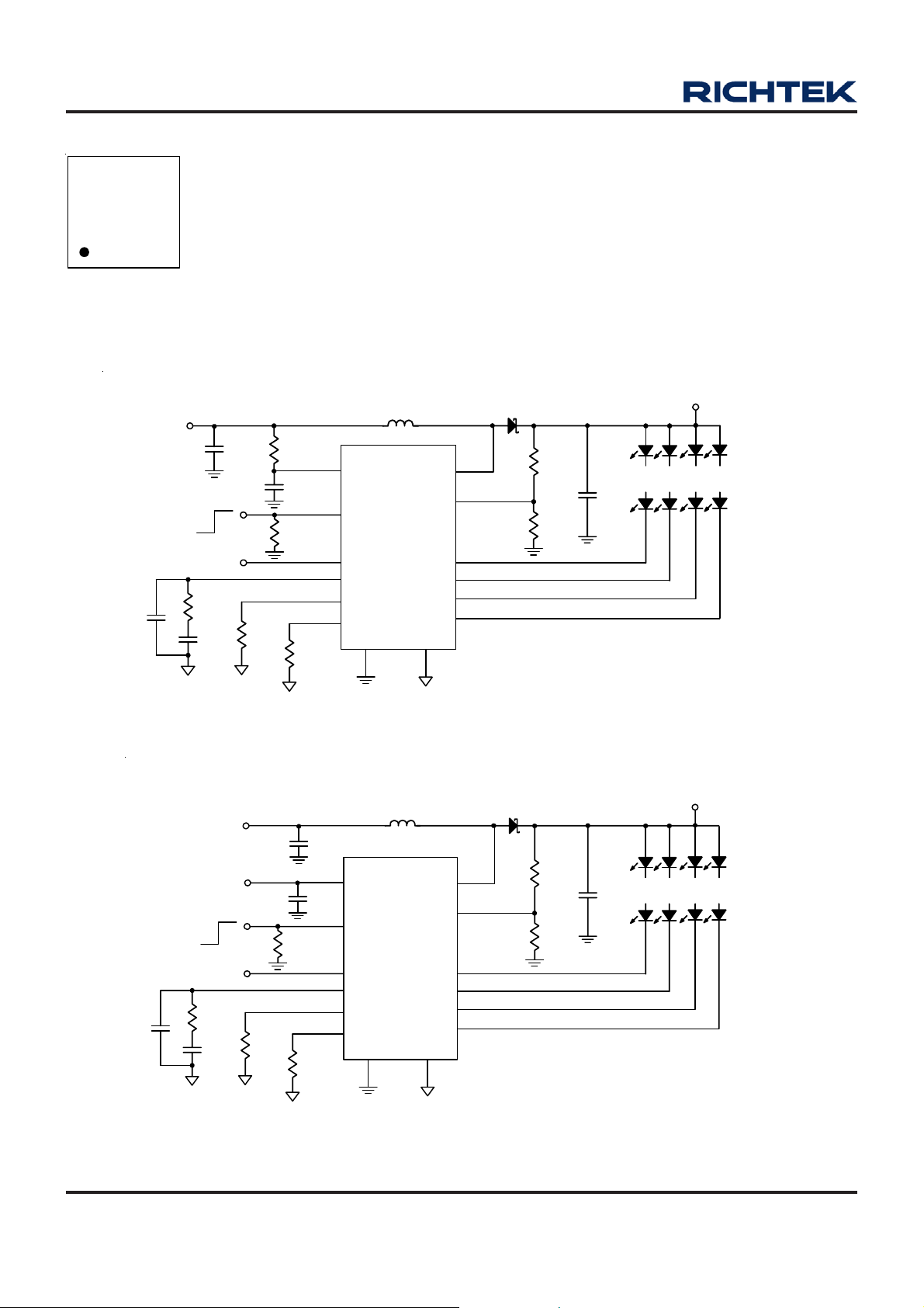
Typical Application Circuit
V
4.2V to 24V
1nF
IN
PWM Dimming
C4
YMDNN : Date Code
C
IN
10µF
Chip Enable
R3
10k
R
C3
10nF
51k
RT
R2
10
C2
1µF
100k
R
ISET
4.75k
7
6
5
2
4
3
VIN
EN
PWM
COMP
RT
ISET
PGND
10, 11
L
10µH
RT8510
AGND
LX
OVP
CH1
CH2
CH3
CH4
1
8, 9
12
13
14
15
16
D1
R
2M
R
62k
OVP2
OVP1
C
OUT
10µF
:
:
:
:
V
OUT
43V MAX
:
:
:
:
:
:
:
:
:
10 LED String
:
:
:
PWM Dimming
C4
1nF
V
BATT
2.7V to 24V
Chip Enable
R3
10k
C3
10nF
5V
R
51k
Figure 1. General Application Circuit
RT
100k
C
10µF
C2
1µF
R
ISET
4.75k
L
10µH
IN
RT8510
7
VIN
6
EN
5
PWM
2
COMP
4
RT
3
ISET
PGND
10, 11
OVP
CH1
CH2
CH3
CH4
AGND
1
LX
12
13
14
15
16
D1
8, 9
Figure 2. Low Input V oltage Application Circuit
R
2M
R
62k
OVP2
OVP1
C
OUT
10µF
(V
depends on D
OUT
:
:
:
:
V
OUT
23V MAX
:
:
:
:
:
:
:
:
)
MAX
:
10 LED String
:
:
:
DS8510-03 June 2011www.richtek.com
2
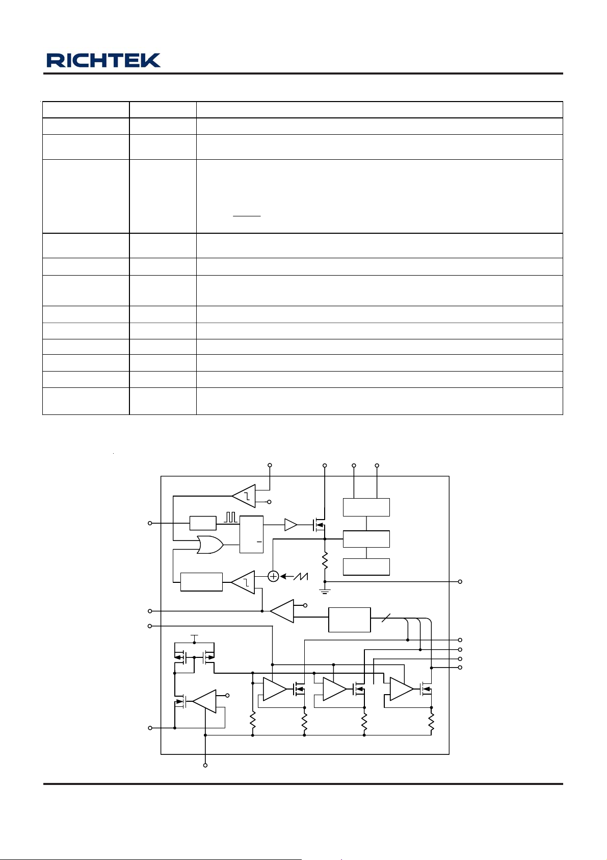
Function Pin Description
Pin No. Pin Name Pin Function
1 AGND Analog Ground of LED Driver.
2 COMP
3 ISET
4 RT
5 PWM Dimming Control Input.
Compensation Pin for Error Amplifier. Connect a compensation network to
ground.
LED Current Set Pin. LED current is set by the value of the resistor R
connected from the ISET pin to ground. Do not short the ISET pin. V
typic al ly 0.6V.
I =
LED
R
95
ISET
Frequency Adj ust Pin. This pin allows setting the switching frequency with a
resistor to 500kHz to 2MHz.
RT8510
ISET
is
ISET
6 EN
Chip Enable (Active High). Note that this pin is high impedance. There should be
a pull low 100kΩ resistor connected to GND when the control signal is floating.
7 VIN Power Supply Input.
8, 9 LX Switching Pin of Boost Converter.
10, 11 PGND P ower Ground of Boost Co nverter.
12 OVP Sense Input for Over Voltage Protection. The detecting threshold is 1.2V.
13, 14, 15, 16 CH1 to CH 4 Current Sink for LED. Leave the pin unconnected, if not used.
17 (Exposed Pad) GND
Th e e xpo se d p ad m us t be s old er e d to a large PC B and c on nec ted to G N D f o r
max imu m pow er dis si pat ion .
Function Block Diagram
RT
COMP
PWM
OSC
PWM
Controller
+
1.2
-
QS
R
Q
+
-
+
EA
-
+
0.6V
+
-
-
0.4V
LXOVP
+
-
EN
Regulator
LED
Detection
OCP
OTP
VIN
:
4
+
:
-
PGND
CH1
CH2
CH3
CH4
ISET
AGND
DS8510-03 June 2011 www.richtek.com
3
RT8510
Absolute Maximum Ratings (Note 1)
z Supply Input V oltage to GND------------------------------------------------------------------------------------------ −0.3V to 26.5V
z EN, PWM, ISET, COMP, RT to GND -------------------------------------------------------------------------------- −0.3V to 26.5V
z LX, OVP , CH1, CH2, CH3, CH4 to GND ---------------------------------------------------------------------------- −0.3V to 48V
z Power Dissipation, P
WQFN-16L 3x3----------------------------------------------------------------------------------------------------------- 1.471W
z Package Thermal Resistance (Note 2)
WQF N-16L 3x3, θJA----------------------------------------------------------------------------------------------------- 68°C/W
WQF N-16L 3x3, θJC----------------------------------------------------------------------------------------------------- 7.5°C/W
z Lead T emperature (Soldering, 10 sec.) ----------------------------------------------------------------------------- 260°C
z Junction T emperature --------------------------------------------------------------------------------------------------- 150°C
z Storage T emperature Range------------------------------------------------------------------------------------------- −65°C to 150°C
z ESD Susceptibility (Note 3)
HBM ------------------------------------------------------------------------------------------------------------------------ 2kV
MM-------------------------------------------------------------------------------------------------------------------------- 200V
Recommended Operating Conditions (Note 4)
@ T
D
= 25°C
A
z Supply Input Voltage, V
z Junction T emperature Range ------------------------------------------------------------------------------------------ −40°C to 125°C
z Ambient T emperature Range ------------------------------------------------------------------------------------------ −40°C to 85°C
---------------------------------------------------------------------------------------------- 4.2V to 24V
IN
Electrical Characteristics
(V
= 4.5V, T
IN
VIN Quiesce nt Current IQ
VIN Shutdown Current I
VIN Under Voltage Lockout UVLO
Control Input
EN, PWM Threshold
Voltage
PWM Dimming Frequency f
EN, PWM Leakage Current I
EN Shutdown Delay tEN R
Boost Converte r
LX On Resistance (N-MOSFET) R
M inimu m O N Time t
M aximum Duty D
LX Current Limit I
= 25°C unless otherwise specified)
A
Parameter Symbol Test Conditions Min Typ Max Unit
V
V
VIN = 4.5V , EN = 0V -- -- 10 μA
SHDN
Rising -- 2.2 -Falling -- 2.1 --
Logic-High VIH 2 -- -Logic-Low V
IL
PWM
2 -- 6 μA
LKG
V
120 -- 30k Hz
= 0V, No Switching -- 1 1.5
COMP
= 2V, Switching 2 3
COMP
mA
V
= 4.2V to 24V
IN
= 51kΩ -- 32 -- ms
RT
-- -- 0.8
V
RRT = 25kΩ -- 2 --
OSC
DS(ON)_N VIN
-- 120 -- ns
MON
MAX
-- 2 -- A
LIM
RRT = 51kΩ -- 1 -- Switching Frequency f
= 102kΩ -- 0.5 --
R
RT
> 4.5V -- 0.2 0.32 Ω
V
COMP
= 2V, Switching -- 90 -- %
MHz
T o be continued
DS8510-03 June 2011www.richtek.com
4

RT8510
Parameter Symbol Test Conditions Min Typ Max Unit
LED Current Programming
2V > CHx > 0.4V Calculating
LED Current Matching I
ISET Pin Voltage V
LED Current I
(I
LEDM
-- 0.6 -- V
ISET
2V > CHx > 0.4V, R
CHx
(MAX)
R
ISET
− I
= 4.75kΩ
(AVG)
) / I
x 100%,
(AVG)
= 4.75kΩ 19.4 20 20.6 mA
ISET
Fault Protection
OVP T hreshold V
OVP F ail Thr eshold V
1.16 1.2 1.24 V
OVP
-- 50 -- mV
OVPF
Thermal Shutdown Temperature TSD -- 160 -- °C
LED Pin Under Voltage
Threshold
Regu la t ed V
Note 1. Stresses listed as the above “Absolute Maximum Ratings” may cause permanent damage to the device. These are for
stress ratings. Functional operation of the device at these or a ny other conditions beyond those indicated in the operation al
sections of the specifications is not implied. Exposure to absolute maximum rating conditions for extended periods may
remain possibility to affect device reliability.
Note 2. θ
Note 3. Devices are ESD sensitive. Handling precaution is recommended.
Note 4. The device is not guaranteed to function outside its operating conditions.
Note 5. Guaranteed by design; not subject to production testing.
is mea sured in natural convection at T
JA
51-7 thermal measurement standard. The measurement case position of θ
V
CHx
No Connection -- 50 -- mV
V
LSD
Highest LE D String Vol tage,
CHx
A
= 4.75kΩ
R
ISET
= 25°C on a high-effective thermal conductivity four-layer test board of JEDEC
is on the exposed pad of the package
JC
-- -- ±2 %
-- 0.4 -- V
DS8510-03 June 2011 www.richtek.com
5

RT8510
Typical Operating Characteristics
Efficiency vs. Input Voltage
100
90
80
70
60
50
40
Efficiency (%)
30
20
10
0
4 8 12 16 20 24
10 x 4 LEDs, f
Input Voltage (V)
LED Current vs. Temperature
26
24
22
OSC
= 1MHz
LED Current vs. Input Voltage
26
24
22
20
18
LED Current ( m A)
16
14
4 9 14 19 24
Input Volt age (V)
V
vs. Temperature
0.70
0.65
0.60
ISET
CH1
CH2
CH3
CH4
f
OSC
= 1MHz
20
18
LED Current ( m A)
16
14
VIN = 12V, f
-50 -25 0 25 50 75 100 125
OSC
Temperature (°C)
V
vs. Input Voltage
0.8
0.7
0.6
ISET
(V)
ISET
0.5
V
0.4
f
0.3
4 8 12 16 20 24
OSC
Input Volt age (V)
= 1MHz
= 1MHz
(V)
0.55
ISET
V
0.50
0.45
0.40
VIN = 12V, f
-50-250 255075100125
OSC
= 1MHz
Temperature (°C)
LED Current vs. PWM Duty Cycle
90
80
70
60
50
40
30
LED Current (mA)
20
10
0
0 102030405060708090100
10 x 4 LEDs, f
Dut y Cycle (%)
PWM = 30kHz
PWM = 10kHz
PWM = 1kHz
PWM = 120Hz
OSC
= 1MHz
DS8510-03 June 2011www.richtek.com
6
RT8510
OVP Threshold vs. Input Voltage
1.5
1.4
1.3
1.2
OVP Threshold (V)
1.1
1.0
4 8 12 16 20 24
Input Voltage (V)
Line Transient Response
f
OSC
= 1MHz
Switch Off Current vs. Temperature
1.5
1.3
1.1
0.9
0.7
Switch Off Current (mA)
f
= 1MHz, VIN = 4.5V
0.5
-50-25 0 25 50 75100125
OSC
Temperature (°C)
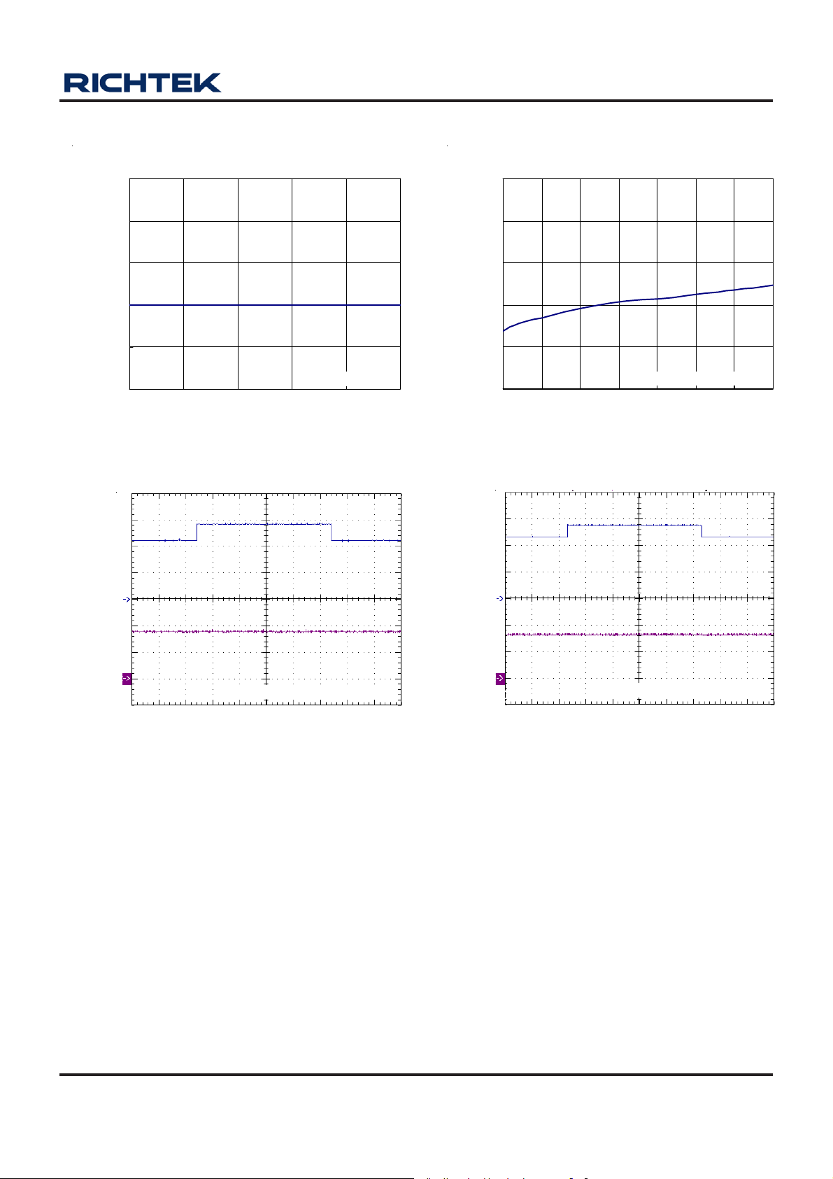
Line Transient Response
V
IN
(5V/Div)
I
OUT
(50mA/Div)
VIN = 11V to 14V, f
Time (50ms/Div)
OSC
= 1MHz
V
IN
(2V/Div)
I
OUT
(50mA/Div)
VIN = 4.5V to 5.5V, f
Time (50ms/Div)
OSC
= 1MHz
DS8510-03 June 2011 www.richtek.com
7
RT8510
Application Information
The RT8510 is a general purpose 4-CH LED driver ca pable
of delivering an adjustable 10 to 40mA LED current. The
IC is a current mode boost converter integrated with a
43V/2A power switch a nd can cover a wide V
4.2V to 24V . The switching frequency is a djustable by an
external resistor from 500kHz to 2MHz. The part
integrates built-in soft start, with PWM dimming control;
moreover, it provides over voltage, over temperature a nd
current limiting protection features.
Soft-Start
The RT8510 equips a built-in soft-start feature to prevent
high inrush current during start-up. The soft-start function
prevents excessive input current and input voltage droop
during power on state.
Compensation
The control loop can be compensates by adjusting the
external components connected to the COMP pin. The
COMP pin is the output of the internal error a mplifier . The
compensation capacitors, C3 and C4, will adjust the
integrator zero and pole respectively to maintain stability .
Moreover, the resistor, R3, will adjust the frequency
integrator gain for fa st tran sient response.
Switching Frequency
range from
IN
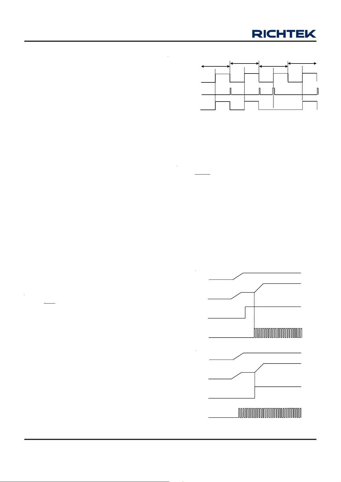
T2
Normal
Operation
T3
Pulse
Skipped
CLK
Output of PWM
Comparator
PWM
Pulse
T1
Normal
Operation
Figure 3. Pulse Skip Mode
Setting and Regulation of LED Current
The LED current can be calculated by the following
equation :
I
LED
where R
95
≅
R
ISET
is the resistor between the ISET pin and GND.
ISET
This setting is the reference for the LED current at channel
1-4 and represents the sensed LED current for ea ch string.
The DC/DC converter regulates the LED current according
to R
ISET
.
Power Sequence
LED Driver is without power sequence concern. Figure 4,
Figure 5 and Figure 6 are different power sequences
respectively . There is no concern in the above condition.
VIN
T4
Normal
Operation
The LED driver switching frequency is able to a djusted as
the following equation :
f (MHz)
OSC
51k
≅
R
RT
LED Connection
The RT8510 equips 4-CH LED divers with ea ch cha nnel
supporting up to 12 LEDs. If the boost converter input
voltage too close to the output voltage, V
increa sed. T o prevent this phenomenon, plea se keep V
ripple will be
OUT
OUT
higher than 1.2 x VIN. The LED strings are connected
from the output of the boost converter to pins 13, 14, 15
and 16 respectively . If one of the LED channel is not used,
the LED pin should be opened directly.
Duty pulse close to minimum on time and small than
120ns, we will skip duty clock. The Figure 3. shows the
pulse skipped time diagram.
8
VOUT
EN
PWM
Power On Mode 1
VIN
VOUT
EN
PWM
Power On Mode 2
Figure 4
DS8510-03 June 2011www.richtek.com

RT8510
VIN
VOUT
EN
PWM
VIN
VOUT
EN
PWM
Power Off Mode 1
Power Off Mode 2
Figure 5
Over Voltage Protection
The RT8510 integrates over voltage protection (OVP)
function. When the voltage at the OVP pin reaches the
threshold voltage, the internal switch will be turned off.
The internal switch will be turned on again once the voltage
at OVP pin drops below its threshold voltage.
The OVP threshold voltage is adjustable and can be
clamped at a certain voltage level a nd it ca n be calculated
by the following equation :
⎛⎞
R
VV1
OUT(OVP) OVP
where V
R
OVP1
=×+
= 1.2V (typ.).
OVP
and R
are the resistors in the voltage divider
OVP2
OVP2
⎜⎟
R
OVP1
⎝⎠
connected to the OVP pin. If at lea st one string is in normal
operation, the controller will automatically ignore the open
strings and continue to regulate the current for the strings
in normal operation. It is suggested to use 2MΩ for R
OVP2
to reduce loading effect.
VIN
VOUT
EN
PWM
VIN
VOUT
EN
PWM
UVLO
Power On Mode 3
UVLO
Power On Mode 3
Figure 6
Current Limit Protection
The RT8510 can limit the peak current to achieve over
current protection. The RT8510 senses the inductor
current during the “ON” period that flows through the LX
pin. The duty cycle depends on the current signal and
internal slope compensation in comparison with the error
signal. The internal switch will be turned off when the
current signal is larger than the internal slope
compensation. In the “OFF” period, the inductor current
will be decrea sed until the internal switch is turned on by
the oscillator.
Brightness Control
The RT8510 brightness dimming control is determined by
the signal on the PWM pin with a suggested PWM
frequency range from 120Hz to 30kHz. However , the LED
current cannot be 100% proportional to duty cycle
especially f or high frequency and low duty ratio because
of physical limitation caused by inductor rising time. Plea se
refer to T a ble 1 and Figure 7.
DS8510-03 June 2011 www.richtek.com
9

RT8510
η
Table 1.
Dimming Frequency (Hz) Duty (Min.) Duty (Max.)
120 < f
500 < f
1k < f
2k < f
5k < f
10k < f
Note : The minimum duty in Table 1 is ba sed on the a pplication
circuit and does not consider the devi ation of current linearity.
≤ 500 0.2% 100%
PWM
≤ 1k 0.4% 100%
PWM
≤ 2k 0.8% 100%
PWM
≤ 5k 1.5% 100%
PWM
≤ 10k 3% 100%
PWM
≤ 30k 10% 100%
PWM
LED Current vs. PWM Duty Cycle
90
80
70
60
50
40
30
LED Current (mA)
20
10
0
0 102030405060708090100
VIN = 12V, V
Dut y Cycle (%)
PWM = 30kHz
PWM = 10kHz
PWM = 1kHz
PWM = 120Hz
= 0V to 3V
PWM
Figure 7
Over Temperature Protection
The RT8510 ha s over temperature protection function to
prevent the IC from overheating due to excessive power
dissipation. The OTP function will shutdown the IC when
junction temperature exceeds 160°C .
Inductor Selection
The value of the inductance L can be a pproximated by the
following equation, where the transition is from
discontinuous conduction mode (DCM) to continuous
conduction mode (CCM) :
D(1D) V
×− ×
L
=
2f I
2
OUT
××
OSC OUT
The duty cycle can be calculated a ccording to the following
equation :
VV
−
OUT IN
D
=
V
OUT
where V
minimum input voltage, f
and I
OUT
is the maximum output voltage, VIN is the
OUT
is the operating frequency
OSC
is the total current from all LED strings.
The boost converter operates in DCM over the entire in put
voltage range when the inductor value is below this value
L. When inductance greater is than L, the converter
operates in CCM at the minimum input voltage a nd may
be discontinuous at higher voltages.
The inductor must be selected with a saturated current
rating that is greater than the peak current provided by
the following equation :
VI VDT
×××
I
PEAK
OUT OUT IN
=+
V2L
××
η
IN
where η is the eff iciency of the power converter a nd T is
the operating period.
Diode Selection
Schottky diodes are recommended for most a pplication s
because of their fa st recovery time a nd low forward voltage.
The power dissipation, reverse voltage rating and pulsating
peak current are the important parameters for Schottky
diode selection. Ma ke sure that the diode's peak current
rating exceeds I
and reverse voltage rating exceeds
PEAK
the maximum output voltage.
Output Capa citor Sele ction
The input ca pacitor reduce s current spikes from the input
supply and minimizes noise in jection to the converter. For
most applications, a 10 μF ceramic ca pa citor is suf ficient.
A value higher or lower may be used depending on the
noise level from the input supply and the input current to
the converter.
For lower output voltage ripple, a low ESR cera mic capa citor
is recommended. The output voltage ripple consists of two
components: one is the pulsating output ripple current
flowing through the ESR, and the other is
VV V
RIPPLE RIPPLE_ESR RIPPLE_C
I R
=+
⎛⎞
IVV
≅×+
PEAK ESR
PEAK AVDD IN1
CVf
⎜⎟
⎝⎠
OUT1 AVDD
−
××
DS8510-03 June 2011www.richtek.com
10
RT8510
)
Thermal Considerations
For continuous operation, do not exceed absolute
maximum junction temperature. The maximum power
dissipation depends on the thermal resistance of the IC
package, PCB layout, rate of surrounding airflow, and
difference between junction and a mbient temperature. The
maximum power dissipation can be calculated by the
following formula :
P
where T
the a mbient temperature, and θ
D(MAX)
= (T
J(MAX)
− TA) / θ
J(MAX)
JA
is the maximum junction temperature, T
is the junction to ambient
JA
A
thermal resistance.
For recommended operating condition specifications of
RT8510, the maximum junction temperature is 125°C a nd
TA is the ambient temperature. The junction to ambient
thermal resistance, θJA, is layout dependent. For WQF N16L 3x3 packages, the thermal resistance, θJA, is 68°C/
W on a standard JEDEC 51-7 f our-layer thermal test board.
The maximum power dissipation at TA = 25°C can be
calculated by the following formula :
P
= (125°C − 25°C) / (68°C/W) = 1.471W for
D(MAX)
WQF N-16L 3x3 pa ckage
The maximum power dissipation depends on the operating
ambient temperature for fixed T
and thermal
J(MAX)
resistance, θJA. For RT8510 pa ckage, the derating curve
in Figure 8 allows the designer to see the effect of rising
ambient te mperature on the maximum power dissipation.
1.60
1.40
Four-Layer PCB
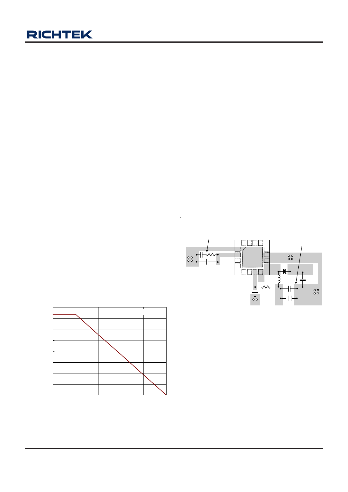
Layout Considerations
PCB layout is very important f or designing switching power
converter circuits. The following layout guides should be
strictly followed for best perf ormance of the RT8510.
` The power components, L1, D1, C
, C
IN
placed a s close a s possible to reduce current loop. The
PCB trace between power components must be a s short
and wide a s possible.
` Place L1 and D1as close as possible to LX pin . The
is
trace should be a s short a nd wide as possible.
` The compensation circuit should be kept away from
the power loops and should be shielded with a ground
trace to prevent any noise coupling. Place the
compensation components as close as possible to
COMP pin.
` The exposed pad of the chip should be connected to
ground plane for thermal con sideration.
The compensation circuit
should be kept away from the
power loops and should be
shielded with a ground trace
to prevent any noise coupling.
GND
C3
C4
R3
AGND
COMP
ISET
RT
CH4
CH3
CH1
CH2
13141516
1
2
GND
3
4
17
8765
LX
EN
VIN
PWM
C2
GND
Place the power components
as close as possible. The
traces should be wide and
short especially for the highcurrent loop.
12
OVP
11
PGND
10
PGND
9
LX
D1
R2
L1
Figure 9. PCB Layout Guide
C
+
V
must be
OUT
IN
IN
V
OUT
C
OUT
GND
1.20
1.00
0.80
0.60
0.40
0.20
Maximum Power Dissipation (W
0.00
0 25 50 75 100 125
Ambient Temperature ( °C)
Figure 8. Derating Curve f or RT8510 Pa ckage
DS8510-03 June 2011 www.richtek.com
11

RT8510
Outline Dimension
D
D2
L
SEE DETAIL A
1
E
e
A
A3
A1
E2
1
b
2
1
2
DET AIL A
Pin #1 ID a nd T ie Bar Mark Options
Note : The configuration of the Pin #1 identifier is optional,
but must be located within the zone indicated.
Dimensions In Millimeters Dimensions In Inches
Symbol
Min Max Min Max
A 0.700 0.800 0.028 0.031
A1 0.000 0.050 0.000 0.002
A3 0.175 0.250 0.007 0.010
b 0.180 0.300 0.007 0.012
D 2.950 3.050 0.116 0.120
D2 1.300 1.750 0.051 0.069
E 2.950 3.050 0.116 0.120
E2 1.300 1.750 0.051 0.069
e 0.500 0.020
L 0.350 0.450
Richtek Technology Corporation
Headquarter
5F, No. 20, Taiyuen Street, Chupei City
Hsinchu, Taiwan, R.O.C.
Tel: (8863)5526789 Fax: (8863)5526611
0.014 0.018
W-Type 16L QFN 3x3 Package
Richtek Technology Corporation
Taipei Office (Marketing)
5F, No. 95, Minchiuan Road, Hsintien City
Taipei County, Taiwan, R.O.C.
Tel: (8862)86672399 Fax: (8862)86672377
Email: marketing@richtek.com
Information that is provided by Richtek Technology Corporation is believed to be accurate and reliable. Richtek reserves the right to make any change in circuit design,
specification or other related things if necessary without notice at any time. No third party intellectual property infringement of the applications should be guaranteed
by users when integrating Richtek products into any application. No legal responsibility for any said applications is assumed by Richtek.
DS8510-03 June 2011www.richtek.com
12

 Loading...