

High Voltage 8-CH LED Driver
RT8561C
General Description
The RT8561C is a 40V 8-CH LED driver capable of
delivering 30mA to each channel with 10 LEDs (3.6V per
diode), for a total of 80 LEDs with one driver. The RT8561C
is a current mode boost converter that operates at 1MHz,
with a wide V
range from 4.5V to 24V and an on chip
IN
current switch rated at 2.5A.
The PWM output voltage loop regulates the LED pins to
0.6V with an auto adjustment circuit allowing voltage
mismatches between LED strings. The RT8561C automati
cally detects and disconnects any unconnected and/or
broken strings during operation from the PWM loop to
prevent V
from over voltage.
OUT
The 1.5% matched LED currents on all channels can be
simply programmed with a resistor or a current sink. A
very high contrast ratio true digital PWM dimming can be
achieved by driving the PWM pin with a PWM signal.
Other protection features include programmable output
over voltage protection, LED current limit, PWM switch
current limit and thermal shutdown.
The RT8561C is available in a WQFN-24L 4x4 package.
Ordering Information
RT8561C
Package Type
QW : WQFN-24L 4x4 (W-Type)
Lead Plating System
G : Green (Halogen Free and Pb Free)
Note :
Richtek products are :
` RoHS compliant and compatible with the current require-
ments of IPC/JEDEC J-STD-020.
` Suitable for use in SnPb or Pb-free soldering processes.
Marking Information
E4= : Product Code
E4=YM
DNN
YMDNN : Date Code
Features
z High Voltage : V
z Programma ble Channel Current from 10mA to 30mA
and Matched to 1.5%
z Current Mode PWM 1MHz Boost Converter
z Easy and High Accuracy Digital Dimming by PWM
Signal
z Programmable Soft-Start
z Automatic Detection of Unconnected and/or Broken
Channel
z Programmable Over Voltage Protection
z Disconnects LED in Shutdown
z No Power Sequence Concern
z V
Under Voltage Lockout
IN
zz
z Over Temperature Protection
zz
zz
z Current Limiting Protection
zz
zz
z Small 24-Lead WQFN Package
zz
zz
z RoHS Compliant and Halogen Free
zz
up to 24V, V
IN
up to 40V
OUT
Applications
z UMPC and Notebook Computer Backlight
z GPS, Portable DVD Backlight
z Desk Lights and Room Lighting
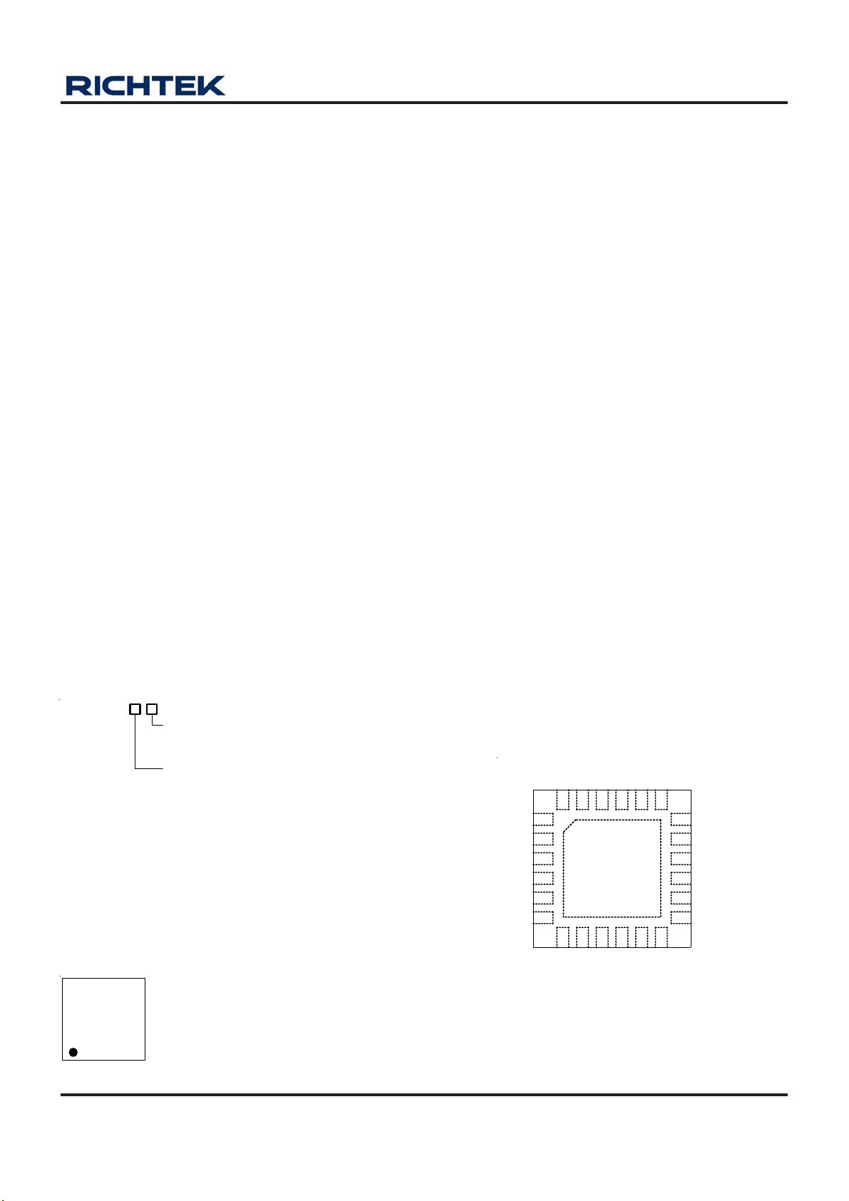
Pin Configurations
(TOP VIEW)
RISET GND
LX
LX
18
VCC
17
CREG
16
LED8
15
LED7
14
NC
LED6
13
EN
25
11
ACTL
LED1
LED2
LED3
LED4
LED5
OVP
GND
GND
24 2223
1
2
3
4
5
6
7
8 9 10 12
VC
NC
WQFN-24L 4x4
GND
21 20 19
GND
SS
DS8561C-00 April 2011 www.richtek.com
1

RT8561C
Typical Application Circuit
L1
VCC
EN5V
ACTL
7
VC
CREG
9
SS
GND
10µH
RT8561C
LX
LED1
LED2
LED7
LED8
OVP
RISET
...
19, 20
1
2
15
16
6
10
I
LED
V
4.5V to 24V
C8
IN
PWM Signal
R1
1.8k
C2
3.9nF
C1
R4
10µF
10
C6
1µF
R5
1k
1k
R6
C3
4.7µF
C4
0.1µF
21, 22, 23, 24,
25 (Exposed Pad)
18
13
11
17
Note :
Due to the limitation of maximum duty, 5V input can support typically to V
D1
R7
R
ISET
4.75k
(mA) =
C5
10µF
C7
...
R(k)
= 33V.
OUT
R2
R3
20 x 4.75
ISET
:
:
:
:
Ω
V
OUT
40V MAX
:
:
...
:
:
:
:
:
:
V
OUT
:
8 x 10 LED String
:
:
:
Figure 1. 1MHz, 20mA Full Scale Current PWM Dimming Control
Function Block Diagram
VCC
OVP
EN
CREG
VC
SS
ACTL
GND
4.2V
1.2V
1.6V
LDO
5V
5µA
+
+
-
+
Shutdown
OSC
S
R
R
+
-
V
OUT
Regulation
Unit
LX
+
-
+
-
LED1
LED2
.
.
.
+
5V
+
-
-
+
-
LED7
LED8
RISET
DS8561C-00 April 2011www.richtek.com
2

Functional Pin Description
Pin No. Pi n Na m e Pin Fun c tion
LED1, LED2,
1, 2, 3, 4, 5
6 OVP
7 VC PWM boost converter loop compensation node.
8 NC No Internal Connection.
9 SS Soft Start Pin, a capacitor of at least 10nF is required for soft start.
10 RISET A resistor or a current from DAC on this pin programs the full LED current.
LED3, LED4,
LED5
Channel 1 to Channel 5 LED current sink. Leave the pin unconnected if not
used.
Over Voltage Protection. PWM boost converter turns off when V
higher than 1.2V.
RT8561C
goes
OVP
11 ACTL
12 NC No Internal Connection.
13 EN Chip enable pin, when pulled low, chip is in shutdown mode.
14, 15, 16
17 CREG
18 VCC Power supply of the chip. For good bypass, a low ESR capacitor is required.
19, 20 LX PWM boost converter switch node.
21, 22, 23, 24,
25 (Exposed Pad)
LED6, LED7,
LED8
GND
Analog/Digital dimming control. When using analog dimming,
I ( mA) = for V 1.2V .
LED ACTL
Channel 6 to Channel 8 LED current sink. Leave the pin unconnected if not
used.
4.7μF capacitor should be placed on this pin to stabilize the 5V output of the
internal regulator. This regulator is for chip internal use only.
Ground pin of the chip. The exposed pad mus t be soldered to a large PCB
and connected to GND for maximum power dissipation.
20 x 4.75
R(k)
ISET
Ω
≥
DS8561C-00 April 2011 www.richtek.com
3
RT8561C
Absolute Maximum Ratings (Note 1)
z Supply Voltage, VCC ----------------------------------------------------------------------------------------------------- 28V
z LX Pin Voltage at Switching Off ---------------------------------------------------------------------------------------- 50V
z LED1 to LED8 Pin--------------------------------------------------------------------------------------------------------- 50V
z ACTL, EN ------------------------------------------------------------------------------------------------------------------- 24V
z OVP -------------------------------------------------------------------------------------------------------------------------- −0.3V to 5.5V
z Power Dissipation, P
WQFN-24L 4x4 ------------------------------------------------------------------------------------------------------------ 1.923W
z Package Thermal Resistance (Note 2)
WQFN-24L 4x4, θJA------------------------------------------------------------------------------------------------------- 52°C/W
WQFN-24L 4x4, θJC------------------------------------------------------------------------------------------------------ 7°C/W
z Junction Temperature ----------------------------------------------------------------------------------------------------- 150°C
z Lead Temperature (Soldering, 10 sec.) ------------------------------------------------------------------------------- 260°C
z Storage Temperature Range -------------------------------------------------------------------------------------------- −65°C to 150°C
z ESD Susceptibility (Note 3)
HBM (Human Body Mode) ---------------------------------------------------------------------------------------------- 2kV
MM (Machine Mode) ------------------------------------------------------------------------------------------------------ 200V
@ TA = 25°C
D
Recommended Operating Conditions (Note 4)
z Supply Input Voltage, VCC---------------------------------------------------------------------------------------------- 4.5V to 24V
z Junction Temperature Range --------------------------------------------------------------------------------------------
z Ambient Temperature Range --------------------------------------------------------------------------------------------
−40°C to 125°C
−40°C to 85°C
Electrical Characteristics
(VCC = 17V, T
Supply Current I
VIN Under Voltage Lockout
Threshold
Shutdown Current I
EN Threshold
Voltage
ACTL Threshold
Voltage
EN Pin Input Current IEN VEN ≤ 5V -- -- 0.1 μA
LED Curre nt Programming
LED Curr ent I
LEDs Current Matching
RISET Pin Voltage V
Input Current of ACTL I
V
Threshold Un-connection -- 0.1 -- V
LED
= 25°C, unless otherwise specified)
A
Parameter Symbol Test Conditions Min Typ Max Unit
VC ≤ 0.2V (Switching off) -- 3 5 mA
VCC
VIN Rising -- 4.2 4.5
Hysteresis -- 0.3 --
VEN = 0V -- -- 10 μA
1.6 -- 5
-- -- 0.65
1.3 -- 5
-- -- 0.65
2V > V
2V > V
Calculating
(I
(MAX)
3.6kΩ ≤ R
V
ACTL
> 0.6V, R
LED
> 0.6V, R
LED
= 4.75kΩ 19 20 21 mA
ISET
= 4.75kΩ
ISET
-- -- 1.5 %
− I
) / I
(MIN)
≤ 9.6kΩ, V
ISET
Average
x 100%
> 1.2V 1.17 1.2 1.23 V
ACTL
= 1.3V -- 1 2 μA
Logic-High V
Logic-Low
Logic-High V
Logic-Low
V
UVLO
SHDN
EN_H
V
EN_L
ACTL_H
V
ACTL_L
LED
RISET
ACTL
To be continued
V
V
V
DS8561C-00 April 2011www.richtek.com
4

RT8561C
Parameter Symbol Test Conditions Min Typ Max Unit
P W M Boos t Conv e r t er
Switching Frequency 0.8 1 1.2 MHz
Minimum On Time -- 100 -- ns
Regulated V
Highest Voltage LED String 0.5 0.6 0.7 V
LED
Amplifier (gm) Output Current 2.4V > VC > 0.2V -- ±15 -- μA
VC Threshold PW M Switch Off 0.1 0.2 -- V
LX R
LX Current Limit I
-- 0.3 0.5 Ω
DS(ON)
2.5 -- -- A
LIM
O VP & So f t St art
OVP Threshold V
OVP Input Curr ent I
1.1 1.2 1.3 V
OVP
V
OVP
≤ 3V -- -- 50 nA
OVP
Soft Start Current ISS VSS ≤ 2.5V 3 5 8 μA
Thermal Shutdown
Temperat ure
-- 150 -- °C
T
SD
Thermal Shutdown Hysteresis -- 20 -- °C
Note 1. Stresses listed as the above “Absolute Maximum Ratings” may cause permanent damage to the device. These are for
stress ratings. Functional operation of the device at these or any other conditions beyond those indicated in the
operational sections of the specifications is not implied. Exposure to absolute maximum rating conditions for extended
periods may remain possibility to affect device reliability.
Note 2. θ
Note 3. Devices are ESD sensitive. Handling precaution is recommended.
Note 4. The device is not guaranteed to function outside its operating conditions.
is measured in the natural convection at TA = 25°C on a high effective four layers thermal conductivity test board of
JA
JEDEC 51-7 thermal measurement standard. The case point of θ
is on the expose pad for the WQFN package.
JC
DS8561C-00 April 2011 www.richtek.com
5

RT8561C
Typical Operating Characteristics
Efficiency vs. Input Voltage
100
90
80
70
60
50
40
Efficiency (%)
30
20
10
0
4 6 8 1012141618202224
Input Voltage (V)
LED Current vs. Temperature
24
23
22
21
20
19
LED Current (mA)
18
17
16
-50 -25 0 25 50 75 100 125
Temperature (°C)
80LEDs
V
= 12V
IN
LED Current vs. Input Voltage
22.0
21.6
21.2
20.8
20.4
20.0
19.6
19.2
LED Current (mA)
18.8
18.4
18.0
4 6 8 1012141618202224
Input Voltage (V)
V
vs. Te mpe rature
1.24
1.22
1.20
1.18
(V)
1.16
RISET
V
1.14
1.12
1.10
-50 -25 0 25 50 75 100 125
RISET
Temperature (°C)
LED1
LED2
LED3
LED4
LED5
LED6
LED7
LED8
V
IN
= 12V
V
vs. Input Voltage
1.25
1.24
1.23
1.22
1.21
(V)
1.20
RISET
1.19
V
1.18
1.17
1.16
1.15
4 6 8 1012141618202224
RISET
25
20
15
10
LED Current (mA)
Input Voltage (V)
LED Curre nt vs. PWM Duty Cycle
PWM = 200Hz
PWM = 1kHz
PWM = 10kHz
PWM = 30kHz
5
V
= 0V to 3V, V
0
0 0.1 0.2 0 .3 0.4 0.5 0.6 0.7 0.8 0.9 1
0 10 20 30 40 50 60 70 80 90 100
PWM
Duty Cycle (%)
IN
= 12V
DS8561C-00 April 2011www.richtek.com
6

RT8561C
Shutdown Current vs. Input Voltage
10
8
6
4
2
Shutdown Current (μA) 1
0
4 6 8 1012141618202224
Input voltage (V)
Switch Off Current vs. Input Voltage
4.0
3.8
3.6
3.4
3.2
3.0
2.8
2.6
2.4
Switch Off Current (mA)
2.2
2.0
4 6 8 1012141618202224
Input Voltage (V)
V
COMP
Shutdown Current vs. Temperature
6
5
4
3
2
Shutdown Current (μA) 1
1
V
= 12V, V
V
= 0V
EN
0
-50 -25 0 25 50 75 100 125
IN
EN
= 0V
Temperature (°C)
SS Current vs. Temperature
8.0
7.6
7.2
6.8
6.4
6.0
5.6
SS Current (μA)
5.2
4.8
= 0V
4.4
4.0
-50 -25 0 25 50 75 100 125
Temperature (°C)
V
IN
= 12V, C
= 0.1μF
SS
SS Current vs. Input Voltage
6.0
5.8
5.6
5.4
SS Current (μA)
5.2
C
5.0
4 6 8 1012141618202224
Input Voltage (V)
= 0.1μF
SS
OVP Voltage (V)
1.30
1.28
1.26
1.24
1.22
1.20
1.18
1.16
1.14
1.12
1.10
OVP Voltage vs. Temperature
V
= 12V
IN
-50 -25 0 25 50 75 100 125
Temperature (°C)
DS8561C-00 April 2011 www.richtek.com
7
RT8561C
1.4
1.2
1.0
0.8
0.6
OVP Voltage (V)
0.4
0.2
0.0
EN
(2V/Div)
OVP Voltage vs. Input Voltage
4 6 8 1012141618202224
Input Voltage (V)
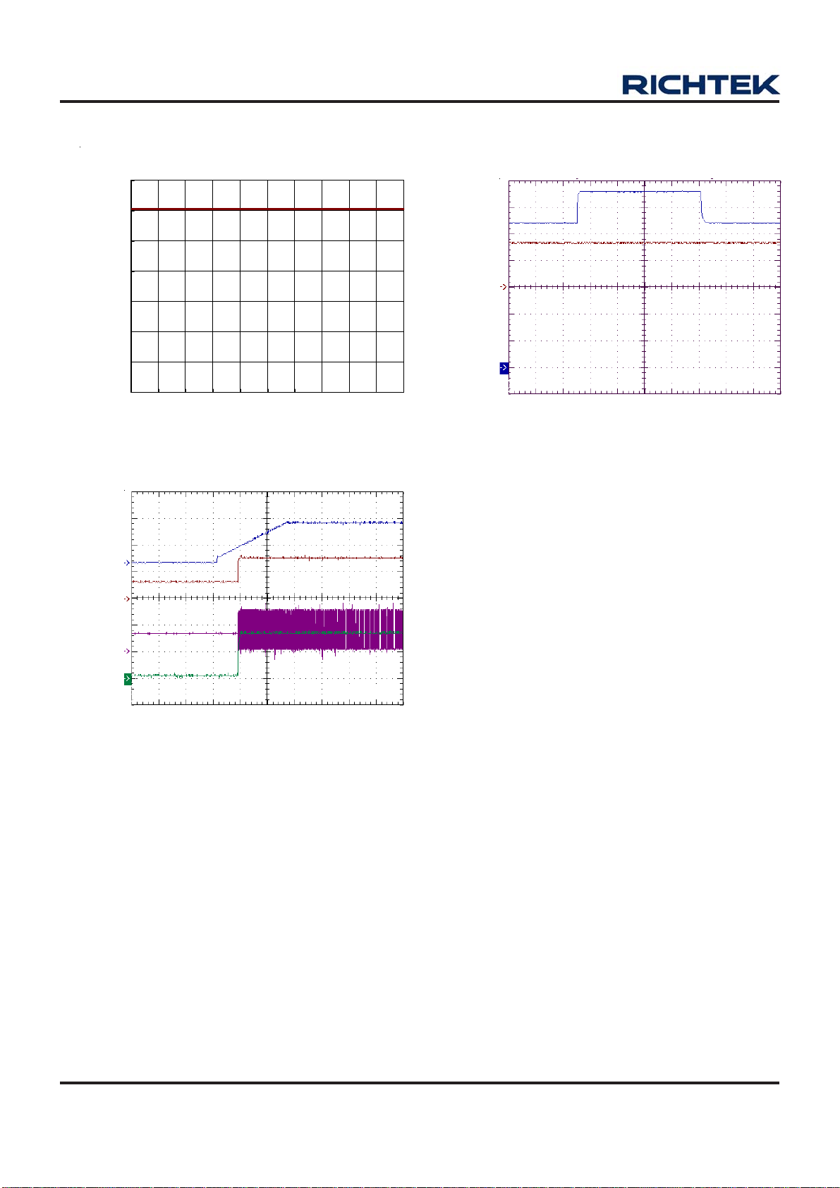
Power On from EN
14V
12V
10V
I
OUT
(100mA/Div)
V
IN
Line Transient Response
V
= 10.8V to 13.2V
IN
Time (50ms/Div)
V
OUT
(20V/Div)
LX
(20V/Div)
I
IN
(100mADiv)
Time (10ms/Div)
V
= 12V
IN
DS8561C-00 April 2011www.richtek.com
8

Applications Information
RT8561C
The RT8561C is a current mode boost converter operating
at 1MHz to power up to 80 white LEDs with a
programmable current for uniform intensity. The part
integrates current sources, soft-start, and easy analog
and digital dimming control. The protection block provides
the circuitry for over temperature, over voltage and current
limit protection features.
Input UVLO
The input operating voltage range of the RT8561C is 4.5V
to 24V. An input capacitor at the VCC pin can reduce
ripple voltage. It is recommended to use a ceramic 10μF
or larger capacitor as the input capacitor. This IC provides
an Under Voltage Lockout (UVLO) function to enhance
the stability during startup.
Soft-Start
The RT8561C employs a soft-start feature to limit the inrush
current. The soft-start circuit prevents excessive inrush
current and input voltage droop. The soft-start time is
determined by the capacitor, C4, which is connected to
the SS pin with 5μA constant current. The value of capacitor
C4 is user defined to satisfy the designer's requirement.
LED Connection
The RT8561C provides an 8-CH LED driver with each
channel capable of supporting up to 10 LEDs. The 8 LED
strings are connected from V
to pins 1, 2, 3, 4, 5, 14,
OUT
15, and 16 respectively. If one of the LED channels is not
in use, the LED pin should be tied to ground directly.
Setting and Regulation of LED Current
The LED current can be calculated by the following
equation :
I(mA) =
LED
where, R
20 x 4.75
R(k)Ω
ISET
is the resistor between the RISET pin and
ISET
GND.
This setting is the reference for the LED current at LED1
to LED8 and represents the sensed LED current for each
string. The DC/DC converter regulates the LED current
according to the setting.
If VIN is close to V
and smaller than V
OUT
, the control
OUT
loop may turn on the power switch with minimum on time
and then skip cycles to maintain LED current regulation.
Brightness Control
The RT8561C features digital dimming control scheme.
A very high contrast ratio true digital PWM dimming can
be achieved by driving the ACTL pin with a PWM signal at
the recommended PWM frequency range from 100Hz to
10kHz.
Dimming frequency can be sufficiently adjusted from
100Hz to 30kHz. However, LED current cannot be 100%
proportional to duty cycle especially for high frequency
and low duty ratio because of physical limitation caused
by inductor rising time. Refer to Table 1 and Figure 2.
Table 1.
Dimming Frequency (Hz) Duty (Min.) Duty (Max.)
100 < f
200 < f
500 < f
1k < f
2k < f
5k < f
10k < f
Note : The minimum duty in Table 1 is based on the application
circuit and does not consider the deviation of current linearity.
≤ 200 0.16% 100%
PWM
≤ 500 0.40% 100%
PWM
≤ 1k 0.80% 100%
PWM
≤ 2k 1.60% 1 00%
PWM
≤ 5k 4.00% 1 00%
PWM
≤ 10k 8.00% 1 00%
PWM
≤ 20k 16.0 0% 100%
PW M
LED Curre nt vs. PWM Duty Cycle
25
20
15
PWM = 200Hz
10
LED Current (mA)
5
V
0
0 0.1 0.2 0 .3 0.4 0.5 0.6 0.7 0.8 0.9 1
0 10 20 30 40 50 60 70 80 90 100
PWM
Duty Cycle (%)
PWM = 1kHz
PWM = 10kHz
PWM = 30kHz
= 0V to 3V, V
IN
= 12V
Figure 2. LED Current vs. PWM Dimming Duty Cycle
DS8561C-00 April 2011 www.richtek.com
9
RT8561C
Over Voltage Protection
The RT8561C equips an Over Voltage Protection (OVP)
function. When the voltage at the OVP pin reaches a
threshold of approximately 1.2V, the MOSFET driver
output (LX) will be turned “OFF”. The MOSFET driver
output (LX) will be turned “ON” again once the voltage at
OVP drops below the threshold voltage 1.2V.
Thus, the output voltage can be clamped at a certain
voltage level as shown in the following equation :
R2
V = V1+
OUT, OVP OVP
⎛⎞
×
⎜⎟
R3
⎝⎠
where
R2 and R3 are the resistors in a voltage divider connected
to the OVP pin.
V
is typically 1.2V.
OVP
If at least one string is in normal operation, the controller
will automatically ignore the open strings and continue to
regulate the current for the string(s) in normal operation.
Current Limit Protection
The RT8561C can limit the peak current to achieve over
current protection. The RT8561C senses the inductor
current through the LX pin during the switch on period.
The duty cycle depends on the current sense signal
summed up with the internal slope compensation and
compared to the VC signal. The internal N-MOSFET will
be turned off when the current signal is larger than the
COMP signal. In the off period, the inductor current will
descend. The internal MOSFET is turned on by the
oscillator in the next beginning cycle.
Hence, even when VIN is ready, the control circuit will
still wait for the arrival of PWM and EN before the LEDs
can react :
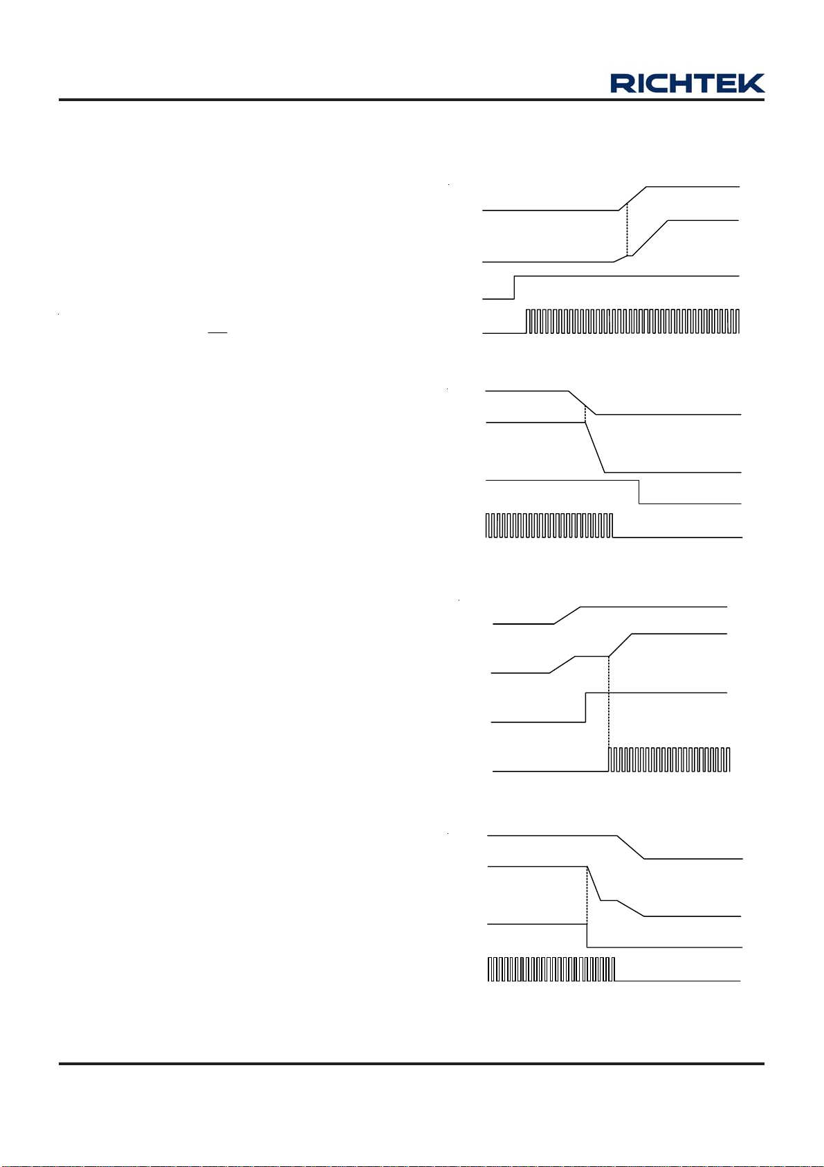
VIN
VOUT
EN
ACTL
UVLO
Figure 3. EN/ACTL Prior to VIN
VIN
VOUT
EN
ACTL
UVLO
Figure 4. VIN Tums Off Prior to EN/ACTL
VIN
VOUT
EN
ACTL
Over Temperature Protection
The RT8561C has an Over Temperature Protection (OTP)
function to prevent excessive power dissipation from
overheating the device. The OTP will shut down switching
operation when the junction temperature exceeds 150°C.
The main converter will start switching again once the
junction temperature cools down approximately by 20°C.
Power Sequence
The RT8561C can apply these power on/off sequences
among VLED, EN and ACTL as shown in the charts below.
10
Figure 5. EN Prior to ACTL Signal
VIN
VOUT
EN
ACTL
Figure 6. EN Prior to ACTL Signal
DS8561C-00 April 2011www.richtek.com

RT8561C
VIN
VOUT
EN
ACTL
Figure 7. ACTL Prior to EN Signal
VIN_POK
ACTL
EN
LED_ON
Figure 8
Inductor Selection
The value of the output inductor (L), where the transition
from discontinuous to continuous mode occurs is
approximated by the following equation :
2
(V V V
OUT IN IN
L =
2I f V
×××
OUT OUT
)
−×
2
Diode Selection
Schottky diode is a good choice for an asynchronous boost
converter due to its small forward voltage. However, when
selecting a Schottky diode, important parameters such
as power dissipation, reverse voltage rating and pulsating
peak current should all be taken into consideration.
Choose a suitable diode with reverse voltage rating greater
than the maximum output voltage.
Capacitor Selection
The input capacitor reduces current spikes from the input
supply and minimizes noise injection into the converter.
For most applications, a 10μF ceramic capacitor is
sufficient. A value higher or lower may be used depending
on the noise level from the input supply and the input
current to the converter.
It is recommended to choose a ceramic capacitor based
on the output voltage ripple requirements. The minimum
value of the output capacitor C
is approximately given
OUT
by the following equation :
(V V ) I
−×
C =
OUT
OUT IN OUT
VVf
η
×××
RIPPLE OUT
where,
V
= maximum output voltage.
OUT
VIN = minimum input voltage.
f = operating frequency.
I
= sum of current from all LED strings.
OUT
η is the efficiency of the power converter.
The boost converter operates in discontinuous mode over
the entire input voltage range when the L1 inductor value
is less than this value L. With an inductance greater than
L, the converter operates in continuous mode at the
minimum input voltage and may be discontinuous at higher
voltages.
The inductor must be selected with a saturation current
rating greater than the peak current provided by the
following equation :
VI VTV V
I =
PEAK
××−
OUT OUT IN OUT IN
η
××
+
V2LV
IN OUT
⎛⎞
⎜⎟
⎝⎠
Thermal Considerations
For continuous operation, do not exceed absolute
maximum junction temperature. The maximum power
dissipation depends on the thermal resistance of the IC
package, PCB layout, rate of surrounding airflow, and
difference between junction and ambient temperature. The
maximum power dissipaton can be calculated by the
following formula :
P
where T
D(MAX)
= (T
J(MAX)
− TA) / θ
J(MAX)
JA
is the maximum junction temperature, TA is
the ambient temperature, and θJA is the junction to ambient
thermal resistance.
For recommended operating condition specifications of
RT8561C, the maximum junction temperature is 125°C
and TA is the ambient temperature. The junction to ambient
thermal resistance, θJA, is layout dependent. For WQFN-
24L 4x4 packages, the thermal resistance, θJA, is 52°C/
W on a standard JEDEC 51-7 four-layer thermal test board.
The maximum power dissipaton at T
= 25°C can be
A
calculated by the following formula :
DS8561C-00 April 2011 www.richtek.com
11

RT8561C
P
= (125°C − 25°C) / (52°C/W) = 1.923W for
D(MAX)
WQFN-24L 4x4 package
The maximum power dissipation depends on the operating
ambient temperature for fixed T
and thermal
J(MAX)
resistance, θJA. For the RT8561C package, the derating
curve in Figure 9 allows the designer to see the effect of
rising ambient temperature on the maximum power
dissipation.
2.40
2.00
1.60
1.20
0.80
0.40
Maximum Power Dissipation (W) 1
0.00
0 25 50 75 100 125
Ambient Temperature (°C)
Four-Layer PCB
LED1
LED2
LED3
LED4
LED5
OVP
C8
Place these components
as close as possible.
D
RISET GND
LX
11
ACTL
LX
25
NC
GND
24 2223
1
2
3
4
5
6
7
VC
R1
C2
GND
GND
GND
21 20 19
GND
8 9 10 12
SS
NC
Locate the compensation
components to VC pin as
close as possible.
Figure 10. PCB Layout Guide
18
17
16
15
14
13
C5
L
VCC
CREG
LED8
LED7
LED6
EN
V
OUT
GND
C1
V
IN
GND
C6
Locate the C6 as
close to VCC pin as
possible.
R4
Figure 9. Derating Curve for RT8561C Package
Layout Guideline
PCB layout is very important for designing power switching
converter circuits. Some recommended layout guides that
should be strictly be followed are shown as follows :
` The power components L
, D1, C
1
VIN1
, C
OUT1
and C
OUT2
must be placed as close as possible to reduce the ac
current loop. The PCB trace between power components
must be short and wide as possible due to large current
flow these trace during operation.
` Place L
and D1 connected to LX pin as close as possible.
1
The trace should be short and wide as possible.
` Recommend place C
` Pin7 is the compensation point to adjust system
close to VCC pin.
VIN2
stability. Place the compensation components to pin7
as close as possible, no matter the compensation is
RC or capacitance.
12
DS8561C-00 April 2011www.richtek.com
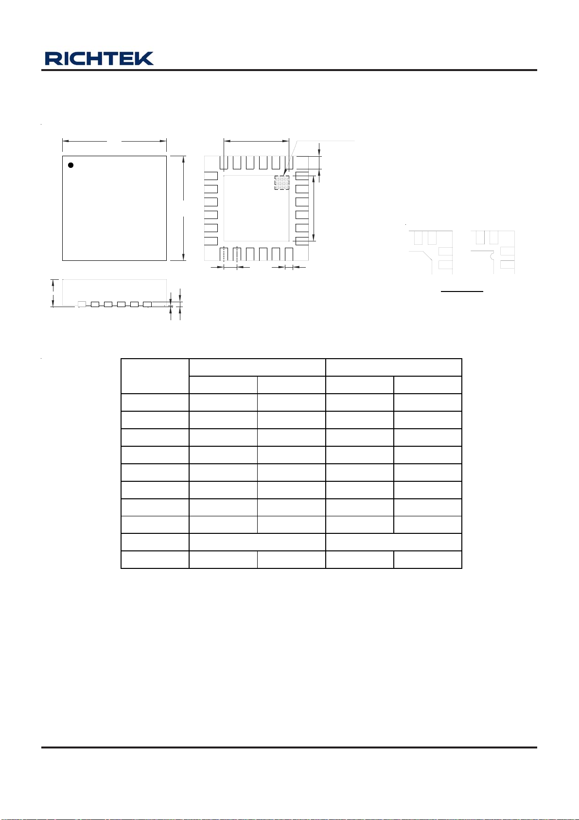
Outline Dimension
RT8561C
D
E
A
A3
A1
D2
SEE DETAIL A
1
be
E2
L
1
2
1
2
DETAIL A
Pin #1 ID and Tie Bar Mark Options
Note : The configuration of the Pin #1 identifier is optional,
but must be located within the zone indicated.
Dimensions In Millimeters Dimensions In Inche s
Symbol
Min Max Min Max
A 0.700 0.800 0.028 0.031
A1 0.000 0.050 0.000 0.002
A3 0.175 0.250 0.007 0.010
b 0.180 0.300 0.007 0.012
D 3.950 4.050 0.156 0.159
D2 2.300 2.750 0.091 0.108
E 3.950 4.050 0.156 0.159
E2 2.300 2.750 0.091 0.108
e 0.500 0.020
L 0.350 0.450
Richtek Technology Corporation
Headquarter
5F, No. 20, Taiyuen Street, Chupei City
Hsinchu, Taiwan, R.O.C.
Tel: (8863)5526789 Fax: (8863)5526611
0.014 0.018
W-Type 24L QFN 4x4 Package
Richtek Technology Corporation
Taipei Office (Marketing)
5F, No. 95, Minchiuan Road, Hsintien City
Taipei County, Taiwan, R.O.C.
Tel: (8862)86672399 Fax: (8862)86672377
Email: marketing@richtek.com
Information that is provided by Richtek Technology Corporation is believed to be accurate and reliable. Richtek reserves the right to make any change in circuit
design, specification or other related things if necessary without notice at any time. No third party intellectual property infringement of the applications should be
guaranteed by users when integrating Richtek products into any application. No legal responsibility for any said applications is assumed by Richtek.
DS8561C-00 April 2011 www.richtek.com
13

 Loading...