

®
High Voltage Multi-Topology LED Driver
RT8463
General Description
The RT8463 is a current mode PWM regulator for LED
driving applications. With a 2A power switch, wide input
voltage (4.5V to 50V) and output voltage (up to 50V)
ranges, the RT8463 can operate in any of the three
common topologies : Buck, Boost or Buck-Boost.
With 470kHz operating frequency, the size of the external
PWM inductor and input/output capacitors can be
minimized. High efficiency is achieved by a 100mV current
sensing control.
Brightness dimming can be controlled from either analog
or PWM signal. A unique built-in clamping comparator
and filtering resistor allow easy low noise analog dimming
conversion from PWM signal with only one external
capacitor.
The RT8463 is available in the TSSOP-14 (Exposed pad)
and WDFN-12L 3x3 packages.
Ordering Information
RT8463
Package Type
CP : TSSOP-14 (Exposed Pad)
QW : WDFN-12L 3x3 (W-Type)
Lead Plating System
G : Green (Halogen Free and Pb Free)
Note :
Richtek products are :
` RoHS compliant and compatible with the current require-
ments of IPC/JEDEC J-STD-020.
` Suitable for use in SnPb or Pb-free soldering processes.
Features
zz
z High Voltage : V
zz
zz
z Buck, Boost or Buck-Boost Operation
zz
zz
z Built-In 2A Power Switch
zz
zz
z Current Mode PWM Control
zz
zz
z 470kHz Fixed Switching Frequency
zz
zz
z Easy Dimming : Analog, PWM Digital or PWM
zz
Up to 50V, V
IN
Up to 50V
OUT
Converting to Analog with One External Capacitor
zz
z Adjustable Soft-Start to Avoid Inrush Current
zz
zz
z Adjustable Over V oltage Protection to Limit Output
zz
Voltage
zz
z Thermal Shutdown
zz
zz
z Under Voltage Lockout
zz
zz
z RoHS Compliant and Halogen Free
zz
Applications
z GPS, Portable DVD Backlight
z Desk Lights and Room Lighting
z Industrial Display Backlight
Marking Information
RT8463GCP
RT8463GCP : Product Number
RT8463
GCPYMDNN
RT8463GQW
98=YM
DNN
YMDNN : Date Code
98 = : Product Code
YMDNN : Date Code
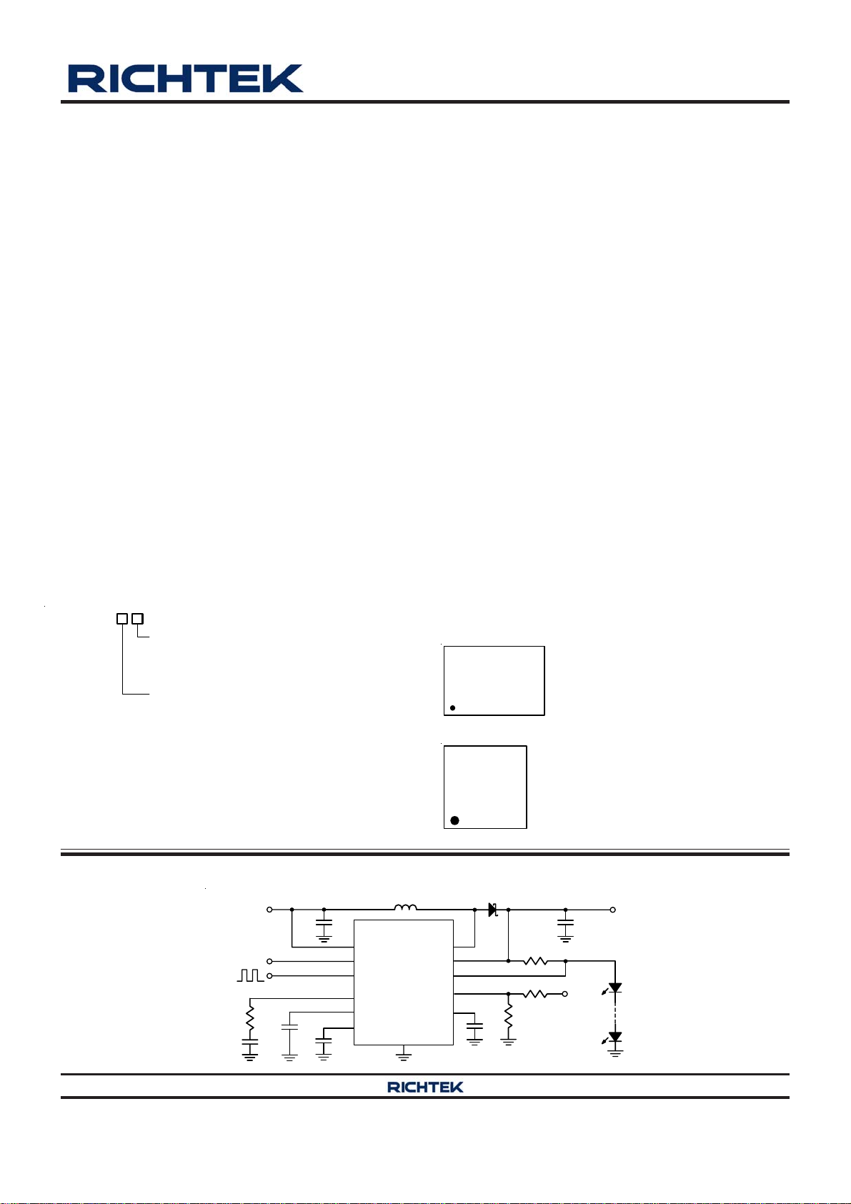
Simplified Application Circuit
V
IN
5V
PWM
Dimming Control
R1
C2
Copyright 2013 Richtek Technology Corporation. All rights reserved. is a registered trademark of Richtek Technology Corporation.
©
C3
C1
VCC
EN
DCTL
VC
SS
ACTL
C4
L
RT8463
SW
ISP
ISN
OVP
CREG
GND
DS8463-00 January 2013 www.richtek.com
D1
C5
R4
R2
R3
V
C6
V
OUT
OUT
1
RT8463
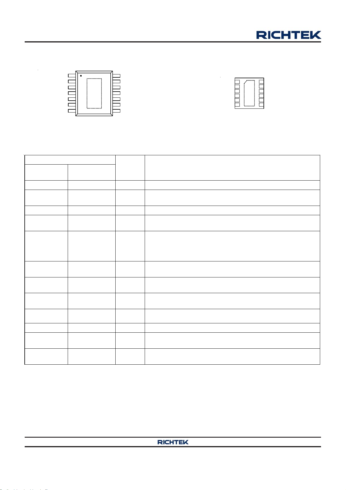
Pin Configurations
ISP
ISN
VC
ACTL
DCTL
EN
GND
2
3
4
GND
5
6
7
(TOP VIEW)
14
VCC
13
CREG
12
SW
11
GND
10
SS
9
15
OVP
8
GND
1
ISP
2
ISN
3
VC
4
ACTL
5
DCTL
67
EN
GND
12
VCC
11
CREG
10
SW
9
GND
8
SS
13
OVP
TSSOP-14 (Exposed Pad)
Functional Pin Description
Pin No.
TSSOP-14
(Exposed Pad)
WDFN-12L 3x3
1 1 ISP Positive Current Sense Input.
2 2 ISN
3 3 VC Compensation Node for PWM Boost Converter Loop.
4 4 ACTL
5 5 DCTL
6 6 EN
7, 8, 11, 15
(Exposed Pad)
13 (Exposed Pad)
9,
9 7 OVP
10 8 SS
12 10 SW Switch Node of PWM Boost Converter.
13 11 CREG
14 12 VCC
Pin Name Pin Function
GND
WDFN-12L 3x3
Negative Current Sense Input. Voltage threshold between ISP and
ISN is 100mV.
Analog Dimming Control Input. Effective programming range is
between 0.2V and 1.2V.
Digital Dimming Control Input. By adding a 0.47μF filtering
capacitor on the ACTL pin, the PWM dimming signal on DCTL pin
will be averaged and converted into analog dimming signal on the
ACTL pin. V
= 1.2V x PWM dimming duty cycle.
ACTL
Enable Control Input (Active High). When this pin is low, the chip is
in shutdown mode.
Ground. The exposed pad must be soldered to a large PCB and
connected to GND for maximum power dissipation.
Over Voltage Protection Sense Input. The PWM Boost converter
turns off when V
goes higher than 1.2V.
OVP
Soft-Start Time Setting. A minimum 10nF capacitor is required for
soft-start.
Regulator Output for Internal Circuit. Placed a 1μF capacitor to
stabilize the 5V output regulator.
Power Supply Voltage Input. For good bypass, a low ESR
capacitor is required.
Copyright 2013 Richtek Technology Corporation. All rights reserved. is a registered trademark of Richtek Technology Corporation.
2
©
DS8463-00 January 2013www.richtek.com
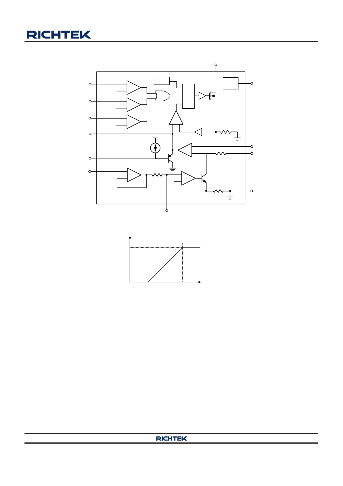
Function Block Diagram
RT8463
SW
VCC
OVP
EN
VC
SS
DCTL
4.5V
1.2V
1.4V
V
ISP
100
+
+
-
+
-
1.2V
+
-
– V
(mV)
ISN
Shutdown
5µA
OSC
ACTL
5V
S
R
R
+
-
-
GM
+
+
-
LDO
CREG
ISN
ISP
GND
V
(V)
0
0.2 1.2
ACTL
Figure 1
Operation
The RT8463 is specifically designed to be operated in
Buck, Boost and Buck-Boost converter applications. This
device uses a fixed frequency, current mode control
scheme to provide excellent line and load regulations. The
control loop has a current sense amplifier to sense the
voltage between the ISP and ISN pins and provides an
output voltage at the VC pin. A PWM comparator then
turns off the internal power switch when the sensed power
switch current exceeds the compensated VC pin voltage.
The power switch will not reset by the oscillator clock in
each cycle. If the comparator does not turn off the switch
in a cycle, the power switch is on for more than a full
Copyright 2013 Richtek Technology Corporation. All rights reserved. is a registered trademark of Richtek Technology Corporation.
DS8463-00 January 2013 www.richtek.com
©
switching period until the comparator is tripped. In this
manner, the programmed voltage across the sense
resistor is regulated by the control loop.
The current through the sense resistor is set by the
programmed voltage and the sense resistance. The voltage
across the sense resistor can be programmed by either
the analog or PWM signals at the ACTL pin, or the PWM
signal at the DCTL pin.
The RT8463 provides protection functions which include
over temperature, input voltage under voltage, output
voltage over voltage, and switch current limit.
3
RT8463
Absolute Maximum Ratings (Note 1)
z Supply Input Voltage, VCC ------------------------------------------------------------------------------------ −0.3V to 60V
z SW Pin Voltage at Switching Off, ISP, ISN ---------------------------------------------------------------- −0.3V to 60V
z DCTL, ACTL, CREG, OVP Pin Voltage -------------------------------------------------------------------- −0.3V to 5.5V (Note 2)
z EN Pin Voltage --------------------------------------------------------------------------------------------------- −0.3V to 20V
z Power Dissipation, P
TSSOP-14 (Exposed Pad) ------------------------------------------------------------------------------------ 3.32W
WDFN-12L 3x3 --------------------------------------------------------------------------------------------------- 3.28W
z Package Thermal Resistance (Note 3)
TSSOP-14 (Exposed Pad), θJA------------------------------------------------------------------------------ 30.1°C/W
TSSOP-14 (Exposed Pad), θJC------------------------------------------------------------------------------ 7.5°C/W
WDFN-12L 3x3, θJA--------------------------------------------------------------------------------------------- 30.5°C/W
WDFN-12L 3x3, θJC--------------------------------------------------------------------------------------------- 7.5°C/W
z Junction Temperature ------------------------------------------------------------------------------------------- 150°C
z Lead Temperature (Soldering, 10 sec.) --------------------------------------------------------------------- 260°C
z Storage Temperature Range ---------------------------------------------------------------------------------- −65°C to 150°C
z ESD Susceptibility (Note 4)
HBM (Human Body Model)------------------------------------------------------------------------------------ 2kV
MM (Machine Model) ------------------------------------------------------------------------------------------- 200V
@ TA = 25°C
D
Recommended Operating Conditions (Note 5)
z Supply Input Voltage, VCC ------------------------------------------------------------------------------------ 4.5V to 50V
z Junction Temperature Range---------------------------------------------------------------------------------- −40°C to 125°C
z Ambient Temperature Range ---------------------------------------------------------------------------------- −40°C to 85°C
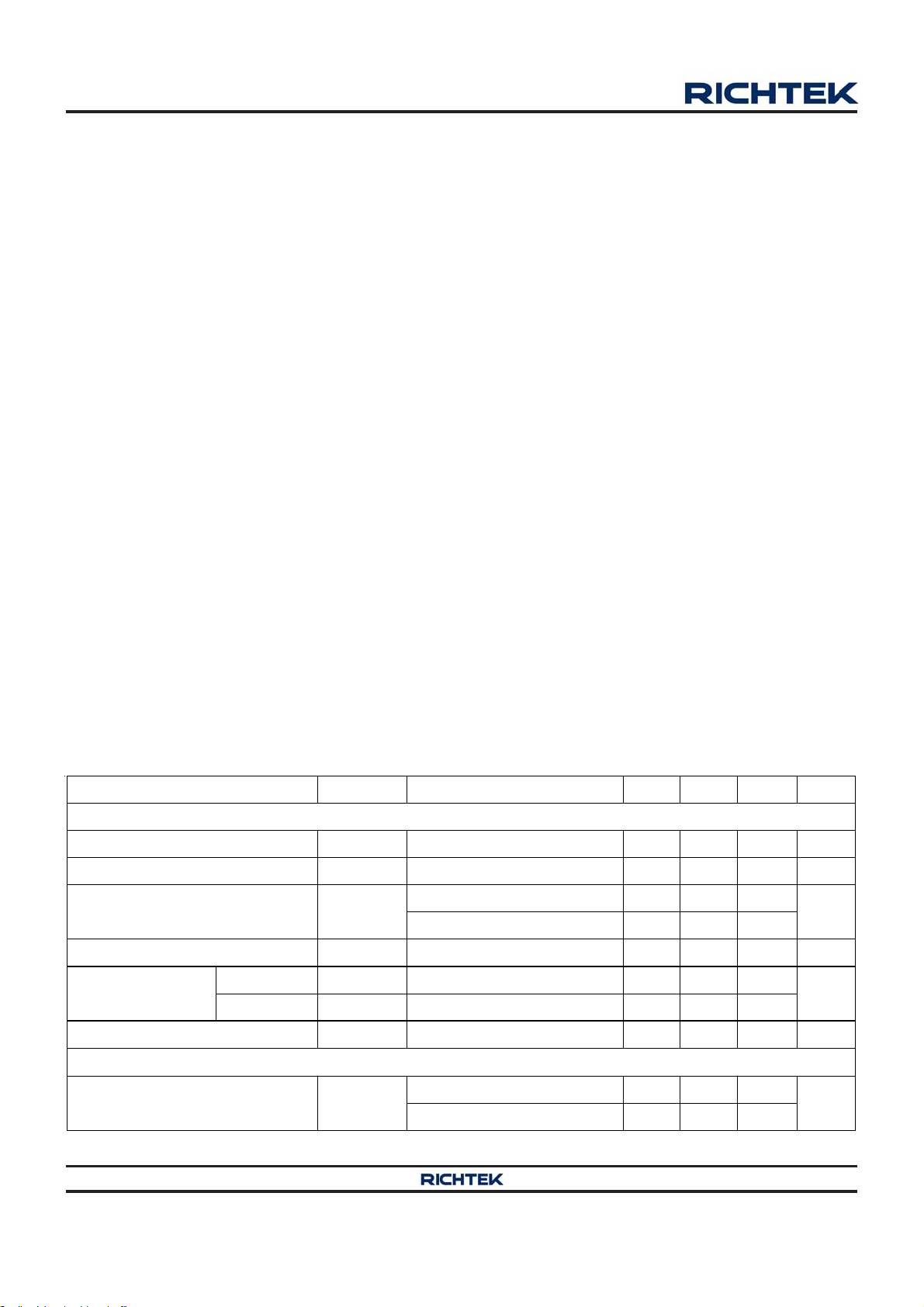
Electrical Characteristics
(VCC = 12V, No Load on any Output, T
Parameter Symbol Test Conditions Min Typ Max Unit
Overall
Regulator Output Voltage V
Supply Current I
VIN Under Voltage Lockout
Threshold
Shutdown Current I
Logic-High V
EN Input Voltage
Logic-Low V
EN Input Current VEN > 2V -- -- 1 μA
Current Sens e Amplifier
= 25°C, unless otherwise specified)
A
I
CREG
VC ≤ 0.2V (Not Switching ) -- -- 5 mA
VCC
= 20mA 4.5 5 5.5 V
CREG
VIN Rising -- 4.2 --
V
UVLO
VEN < 0.5V -- -- 15 μA
SHDN
2 -- --
EN_H
-- -- 0.5
EN_L
Falling -- 3.8 --
V
IN
V
V
V
≥ 1.25V 96 100 102
Input Threshold (V
ISP
− V
)
ISN
ACTL
= 1.2V 95 98 101
V
ACTL
Copyright 2013 Richtek Technology Corporation. All rights reserved. is a registered trademark of Richtek Technology Corporation.
4
©
DS8463-00 January 2013www.richtek.com
mV
RT8463
Parameter Symbol Test Conditions Min Typ Max Unit
Input Current I
Input Current I
Output Current IVC 2V > VC > 0. 2V -- ±10 -- μA
VC Threshold for PWM Switch Off -- 0.2 -- V
LED Dimming
Analog Dimming ACTL Pin Input
Current
LED C ur rent On Threshold at
ACTL
LED C ur rent Off Threshold at
ACTL
DCTL Input Current I
DCTL Input
Voltage
Logic-High V
Logic-Low V
PWM Boost Converter
Switching Frequency fSW 420 470 520 kHz
V
ISP
V
ISN
I
0 ≤ V
ACTL
V
ACTL_ON
V
ACTL_OFF
DCTL
DCTL_H
DCTL_L
(V
-- 0.2 0.25 V
0.3V ≤ V
2 -- --
-- -- 0.1
= 24V -- 200 -- μA
ISP
= 24V -- 20 -- μA
ISN
≤ 3V, DCTL Floating -- -- 2 μA
ACTL
ISP
− V
) = 100mV -- 1.2 1.33 V
ISN
≤ 5V -- 0.5 2 μA
DCTL
V
Maximum Duty Cycle D
-- -- 100 %
MAX
Minimum On-Time (Note 6) -- 150 250 ns
SW R
SW Current Limit I
-- 0.3 0.5 Ω
DS(ON)
LIM_SW
2 2.5 -- A
OVP and Soft-Start
OVP Threshold V
OVP Input Current I
Soft-Start SS Pin Current ISS V
1.15 1.2 1.25 V
OVP
V
OVP
≤ 1.5V -- -- 50 nA
OVP
≤ 2.5V -- 5 8 μA
SS
Temperature Protection
Thermal Shutdown Temperature
Thermal Shutdown Hysteresis
Note 1. Stresses beyond those listed “Absolute Maximum Ratings” may cause permanent damage to the device. These are
stress ratings only, and functional operation of the device at these or any other conditions beyond those indicated in
the operational sections of the specifications is not implied. Exposure to absolute maximum rating conditions may
affect device reliability.
Note 2. If connected with a 20kΩ serial resistor, ACTL and DCTL can go up to 40V.
Note 3. θ
Note 4. Devices are ESD sensitive. Handling precaution is recommended.
Note 5. The device is not guaranteed to function outside its operating conditions.
Note 6. Guaranteed by design, not subjected to production test.
is measured at T
JA
measured at the exposed pad of the package.
= 25°C on a high effective thermal conductivity four-layer test board per JEDEC 51-7. θJC is
A
T
SD
ΔT
SD
-- 150 -- °C
-- 20 -- °C
Copyright 2013 Richtek Technology Corporation. All rights reserved. is a registered trademark of Richtek Technology Corporation.
DS8463-00 January 2013 www.richtek.com
©
5
RT8463
Typical Application Circuit
V
4.5V to 50V
PWM
Dimming control
4.5V to 50V
IN
5V
R1
10k
C2
3.3nF
V
IN
Analog
Dimming
5V
R1
10k
C2
3.3nF
D1
C1
R2
100mV
C5
1µF
L
22µH
C3
10nF
C4
0.47µF
VCC
EN
DCTL
VC
SS
ACTL
RT8463
ISP
ISN
OVP
GND
CREG
SW
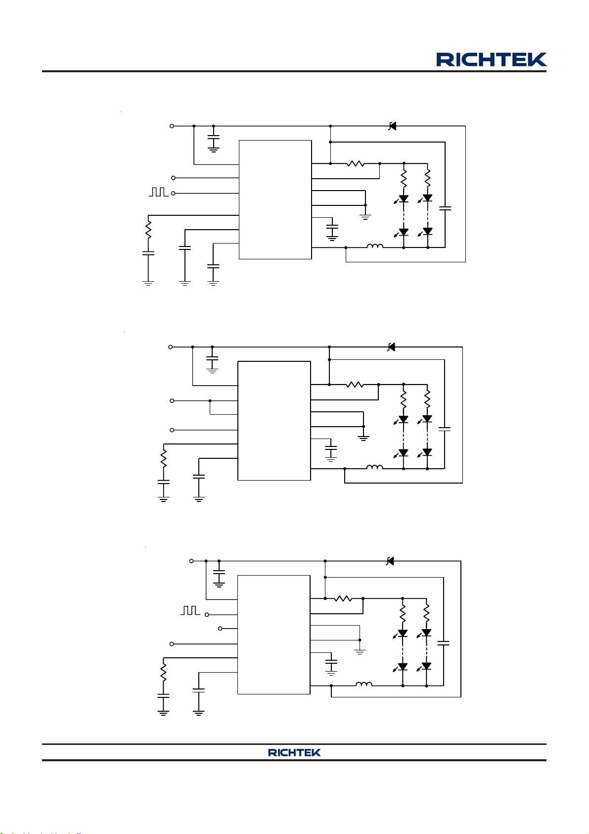
Figure 2. PWM to Analog Dimming Buck Configuration
D1
C1
R2
100mV
C5
1µF
L
15µH
C3
10nF
VCC
ACTL
DCTL
EN
VC
SS
RT8463
ISP
ISN
OVP
GND
CREG
SW
R3 R4
C6
R3 R4
C6
Figure 3. Analog Dimming Buck Configuration
V
4.5V to 50V
IN
PWM
Dimming control
5V
R1
10k
C2
3.3nF
C3
10nF
C1
VCC
ACTL
DCTL
EN
VC
SS
RT8463
ISP
ISN
OVP
GND
CREG
SW
R2
100mV
C5
1µF
15µH
D1
R3 R4
C6
L
Figure 4. PWM Dimming Buck Configuration Through ACTL Pin
Copyright 2013 Richtek Technology Corporation. All rights reserved. is a registered trademark of Richtek Technology Corporation.
6
©
DS8463-00 January 2013www.richtek.com

V
5V
R1
10k
C2
3.3nF
IN
4.5V to 50V
PWM
Dimming control
Figure 5. PWM to Analog Dimming Boost Configuration
C3
10nF
C1
C4
0.47µF
VCC
EN
DCTL
VC
SS
ACTL
L
15µH
RT8463
SW
ISP
ISN
GND
CREG
OVP
D1
C5
1µF
100mV
R4
R2
R3
C6
V
C6
1µF
OUT
V
OUT
50V (Max.)
RT8463
V
R1
10k
C2
3.3nF
IN
5V
4.5V to 50V
PWM
Dimming control
Figure 6. PWM to Analog Dimming Buck-Boost Configuration
C3
10nF
C1
C4
0.47µF
VCC
EN
DCTL
VC
SS
ACTL
RT8463
SW
ISP
ISN
GND
CREG
OVP
L
15µH
R2
100mV
C5
1µF
R4
R3
D1
V
OUT
V
OUT
50V (Max.)
Copyright 2013 Richtek Technology Corporation. All rights reserved. is a registered trademark of Richtek Technology Corporation.
©
DS8463-00 January 2013 www.richtek.com
7

RT8463
)
)
Typical Operating Characteristics
Supply Current vs. VCC
2.5
2.0
1.5
1.0
Supply Current (mA
0.5
0.0
0 5 10 15 20 25 30 35 40 45 50
VCC (V)
Shutdown Current vs. VCC
8.0
7.5
7.0
6.5
6.0
5.5
Supply Current v s . Te mp erature
2.2
2.0
1.8
1.6
Supply Current (mA
1.4
V
= 12V
1.2
-50-25 0 25 50 75100125
CC
Temperature (°C)
ISP-ISN Threshold vs. Te m pe rature
130
118
106
94
5.0
Shutdown Current (μA) 1
4.5
4.0
0 1020304050
VCC (V)
Efficiency vs. Input Voltage
100
Boost
95
90
85
Efficiency (%)
80
V
= 30V, I
OUT
75
5 1015202530
Input Voltage (V)
OUT
= 210mA
82
ISP-ISN Threshold (mV)
V
= 12V
70
-50-25 0 25 50 75100125
IN
Temp erature (° C)
Efficiency vs. Input Voltage
100
Buck
95
90
85
Efficiency (%)
80
V
= 15V, I
OUT
75
15 18 21 24 27 30
Input Voltage (V)
OUT
= 210mA
Copyright 2013 Richtek Technology Corporation. All rights reserved. is a registered trademark of Richtek Technology Corporation.
©
DS8463-00 January 2013www.richtek.com
8

100
95
Efficiency vs. Input Voltage
Buck-Boost
240
210
180
I
OUT
vs. V
RT8463
ACTL
90
85
Efficiency (%)
80
V
= 15V, I
75
4 6 8 101214161820
OUT
OUT
= 210mA
Input Voltage (V)
I
vs. V
240
OUT
210
180
150
120
DCTL
(mA)
90
OUT
I
60
30
0
0 102030405060708090100
V
OUT
= 30V, I
= 210mA, f = 100Hz
OUT
PWM Duty (%)
150
120
(mA)
OUT
I
90
60
30
0
0 0.3 0.6 0.9 1.2 1.5
V
vs. Temperature
1.4
1.3
1.2
(V)
1.1
OVP
V
1.0
0.9
0.8
-50 -25 0 25 50 75 100 125
OVP
V
ACTL
V
(V)
OUT
= 30V, I
OUT
Temp erature (°C)
= 210mA
V
= 12V
CC
Frequency vs. VCC
480
470
460
450
440
Frequency (kHz) 1
430
420
0 5 10 15 20 25 30 35 40 45 50
VCC (V)
Copyright 2013 Richtek Technology Corporation. All rights reserved. is a registered trademark of Richtek Technology Corporation.
©
6.2
5.8
5.4
5.0
SS Current (µA)
4.6
4.2
-50-25 0 25 50 75100125
SS Current vs. Temperature
V
Temperature (°C)
CC
= 12V
DS8463-00 January 2013 www.richtek.com
9

RT8463
I
OUT
(200mA/Div)
V
OUT
(20V/Div)
V
IN
(10V/Div)
Power On from VIN
Time (25ms/Div)
I
OUT
(200mA/Div)
V
OUT
(20V/Div)
V
IN
(10V/Div)
Power Off from VIN
Time (250ms/Div)
Copyright 2013 Richtek Technology Corporation. All rights reserved. is a registered trademark of Richtek Technology Corporation.
©
DS8463-00 January 2013www.richtek.com
10

Application Information
RT8463
Loop Compensation
The RT8463 has an external compensation pin (VC)
allowing the loop response optimized for specific
application. An external resistor in series with a capacitor
is connected from the VC pin to GND to provide a pole
and a zero for proper loop compensation. The
recommended compensation resistance and capacitance
for the RT8463 are 10kΩ and 3.3nF.
Soft-Start
The soft-start can be achieved by connecting a capacitor
from the SS pin to GND. The built-in soft-start circuit
reduces the start-up current spike and output voltage
overshoot. The soft-start time is determined by the external
capacitor charged by an internal 5μA constant charging
current. The SS pin directly limits the slew rate of voltage
on the VC pin, which in turn limits the peak switch current.
The value of the soft-start capacitor is user defined to
satisfy the designer's requirements.
LED Current Setting
Output Over Voltage Setting
The RT8463 is equipped with Over Voltage Protection
(OVP) function. When the voltage at OVP pin exceeds a
threshold of approximately1.2V, the power switch is turned
off. The power switch can be turned on again once the
voltage at OVP pin drops below 1.2V.
For the Boost application, the output voltage could be
clamped at a certain voltage level. The OVP voltage can
be set by the following equation :
V = 1.2(1 + )
OUT_OVP
where R3 and R4 are the voltage divider from V
R3
×
R4
to GND
OUT
with the divider center node connected to the OVP pin.
Current Limit Protection
The RT8463 can limit the peak switch current by the
internal over current protection feature. In normal operation,
the power switch is turned off when the switch current
reaches the loop-set value. The maximum peak-current
limit of the switch is 2.5A (typ.).
The LED current could be calculated by the following
equation :
I =
LED(MAX)
V (ISP ISN)
−
R2
where V (ISP − ISN) is the voltage between ISP and ISN
(100mV typ. if ACTL or DCTL dimming is not applied) and
the R2 is the resister between ISP and ISN.
Brightness / Dimming Control
The RT8463 features both analog and digital dimming
control. Analog dimming is linearly controlled by an
external voltage (0.2V < V
< 1.2V). With an on-chip
ACTL
output clamping amplifier and a resistor, PWM dimming
signal fed at DCTL pin can be easily filtered to an analog
dimming signal with an external capacitor from the ACTL
pin to GND for noise-free PWM dimming. A very high
contrast ratio true digital PWM dimming can be achieved
by driving the ACTL pin with a PWM signal from 100Hz to
10kHz.
Over Temperature Protection
The RT8463 provides Over Temperature Protection (OTP)
function to prevent the excessive power dissipation from
overheating. The OTP function will shut down switching
operation when the die junction temperature exceeds
150°C. The chip will automatically start to switch again
when the die junction temperature cools off.
Inductor Selection
Choose an inductor that can handle the necessary peak
current without saturating, and ensure that the inductor
has a low DCR (copper wire resistance) to minimize I2R
power losses. Inductor manufacturers specify the
maximum current rating as the current where the
inductance falls to certain percentage of its nominal value
(65% typ.).
Copyright 2013 Richtek Technology Corporation. All rights reserved. is a registered trademark of Richtek Technology Corporation.
DS8463-00 January 2013 www.richtek.com
©
11

RT8463
Table 1. Relevant Parameters for Buck, Boost, and Buck
Buck Boost Buck − Boost
V
OUT
Duty Cycle : D
Average Inductor
Current : I
L
ΔI (A)
Δ
I (A)
=
γ
I (A) = I (1 )
PK L
I
L
×+
γ
2
L (H)
VV
IN F
I
+
VV
OUT F
×
Lf
SW
+
VV
OUT F
××
ILf
OUT SW
×+
I(1)
OUT
+
VV
OUT F
××
If
γ
OUT SW
+
OUT
×−
(1 D)
×−
(1 D)
γ
×+
2
×−
(1 D)
γ : Current ripple ratio, set γ = 1 for typical peak current
disign.
fSW : Switch Frequency
VF : Forward voltage drop of the output rectifier.
VIN : Nominal input voltage.
V
: Desired output voltage.
OUT
I
: Desired output current.
OUT
IPK : Peak current of Inductor.
L : Minimum Desired Inductor value.
Table1, shows the relevant parameters for Buck, Boost
and Buck − Boost topologies. The first column is for the
basic definition of the terms.
The peak inductor current depends on the different
topologies. For a Buck converter the average value of the
inductor current equals the load current, irrespective of
the input voltage. When as the input increases, the peak
current increases.
The inductor must be selected with a saturation current
rating greater than the peak current limit.
−−
− Boost Topologies
−−
−+
VVV
OUT IN F
+
VV
OUT F
I
OUT
1D
−
+
VV
OUT F
×
Lf
VV
OUT F
××
ILf
OUT SW
I
1D 2
VV
OUT F
××
If
OUT SW
SW
+
OUT
−
+
γ
×−
D (1 D)
×−
D (1 D)
γ
(1 )
×−
D (1 D)
2
×+
2
VV V
IN OUT F
VV
OUT F
Lf
VV
OUT F
××
ILf
OUT SW
I
OUT
1D 2
VV
OUT F
××
If
OUT SW
+
VV
OUT F
++
I
OUT
1D
−
+
×−
×
SW
+
−
+
γ
(1 D)
×−
(1 D)
γ
(1 )
×−
(1 D)
Schottky Diode Selection
The Schottky diode, with low forward voltage drop and
fast switching speed, is necessary for the RT8463
applications. In addition, power dissipation, reverse voltage
rating and pulsating peak current are the important
parameters of the Schottky diode that must be
considered. Choose a suitable Schottky diode whose
reverse voltage rating is greater than the maximum output
voltage. The diode's average current rating must exceed
the average output current. The diode conducts current
only when the power switch is turned off (typically less
than 50% duty cycle).
Capacitor Selection
The input capacitor reduces current spikes from the input
supply and minimizes noise injection to the converter. For
most RT8463 applications, a 4.7μF ceramic capacitor is
sufficient. A higher or lower value may be used depending
on the noise level from the input supply and the input
current to the converter.
In Boost application, the output capacitor is typically a
ceramic capacitor and is selected based on the output
voltage ripple requirements. The minimum value of the
output capacitor, C
, is approximately given by the
OUT
following equation :
××
IDT
C =
OUT
LED
V
RIPPLE
2
2
Copyright 2013 Richtek Technology Corporation. All rights reserved. is a registered trademark of Richtek Technology Corporation.
12
©
DS8463-00 January 2013www.richtek.com

RT8463
Thermal Considerations
For continuous operation, do not exceed absolute
maximum junction temperature. The maximum power
dissipation depends on the thermal resistance of the IC
package, PCB layout, rate of surrounding airflow, and
difference between junction and ambient temperature. The
maximum power dissipation can be calculated by the
following formula :
P
where T
the ambient temperature, and θ
D(MAX)
= (T
J(MAX)
− TA) / θ
J(MAX)
JA
is the maximum junction temperature, TA is
is the junction to ambient
JA
thermal resistance.
For recommended operating condition specifications, the
maximum junction temperature is 125°C. The junction to
ambient thermal resistance, θJA, is layout dependent. For
TSSOP-14 (Exposed Pad) package, the thermal
resistance, θJA, is 30.1°C/W on a standard JEDEC 51-7
four-layer thermal test board. For WDFN-12L 3x3 package,
the thermal resistance, θJA, is 30.5°C/W on a standard
JEDEC 51-7 four-layer thermal test board. The maximum
power dissipation at TA = 25°C can be calculated by the
following formula :
P
= (125°C − 25°C) / (30.1°C/W) = 3.32W for
D(MAX)
TSSOP-14 (Exposed Pad) package
P
= (125°C − 25°C) / (30.5°C/W) = 3.28W for
D(MAX)
WDFN-12L 3x3 package
The maximum power dissipation depends on the operating
ambient temperature for fixed T
and thermal
J(MAX)
resistance, θJA. The derating curve in Figure 7 allows the
designer to see the effect of rising ambient temperature
on the maximum power dissipation.
3.5
3.0
2.5
2.0
1.5
1.0
0.5
TSSOP-14 (Exposed Pad)
WDFN-12L 3x3
Four-Layer PCB
Maximum Power Dissipation (W) 1
0.0
0 25 50 75 100 125
Ambient Temperature (°C)
Figure 7. Derating Curve of Maximum Power Dissipation
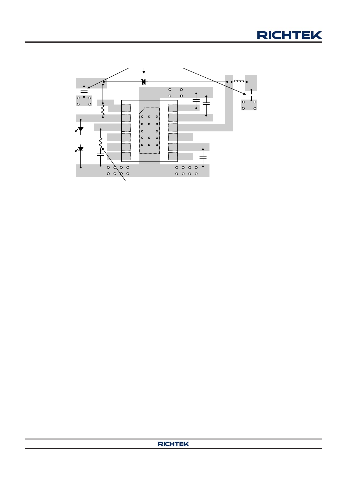
Layout Consideration
PCB layout is very important to design power switching
converter circuits. The recommended layout guidelines
are listed as follows :
` The power components L1, D1, C
VIN
, and C
OUT
must be
placed as close to each other as possible to reduce the
ac current loop area. The PCB trace between power
components must be as short and wide as possible
due to large current flow through these traces during
operation.
` Place L1 and D1 connected to SW pin as close as
possible. The trace should be as short and wide as
possible.
` The input capacitors C1 must be placed as close to
VCC pin as possible.
` Place the compensation components to the VC pin as
close as possible to avoid noise pick up.
Copyright 2013 Richtek Technology Corporation. All rights reserved. is a registered trademark of Richtek Technology Corporation.
DS8463-00 January 2013 www.richtek.com
©
13
RT8463
Place these components as close as possible.
GND
:
:
:
:
D1
C
OUT
1
R
C
SENS
R
VC
VC
ISP
2
ISN
3
VC
4
ACTL
DCTL SS
5
6
GND
Grand PlaneEN
GND
Locate the compensation components to VC
pin as close as possible.
Figure 8. PCB Layout Guide for WDFN-12L 3x3
GND
12
11
10
9
8
7
C1
VCC
CREG
SW
GND
OVP
VIN
L1
C
VIN
C5
GND
Locate input
capacitor to
VCC as close
as possible.
C
SS
Copyright 2013 Richtek Technology Corporation. All rights reserved. is a registered trademark of Richtek Technology Corporation.
©
DS8463-00 January 2013www.richtek.com
14

Outline Dimension
RT8463
Symbol
A 1.000 1.200 0.039 0.047
A1 0.000 0.150 0.000 0.006
A2 0.800 1.050 0.031 0.041
b 0.190 0.300 0.007 0.012
D 4.900 5.100 0.193 0.201
e 0.650 0.026
E 6.300 6.500 0.248 0.256
E1 4.300 4.500 0.169 0.177
L 0.450 0.750 0.018 0.030
U 1.900 2.900 0.075 0.114
V 1.600 2.600 0.063 0.102
Dimensions In Millimeters Dimensions In Inches
Min Max Min Max
14-Lead TSSOP (Exposed Pad) Plastic Package
Copyright 2013 Richtek Technology Corporation. All rights reserved. is a registered trademark of Richtek Technology Corporation.
DS8463-00 January 2013 www.richtek.com
©
15

RT8463
2
1
DETAIL A
Pin #1 ID and Tie Bar Mark Options
Note : The configuration of the Pin #1 identifier is optional,
but must be located within the zone indicated.
Dimensions In Millimeters Dimensions In Inches
Symbol
Min Max Min Max
A 0.700 0.800 0.028 0.031
A1 0.000 0.050 0.000 0.002
A3 0.175 0.250 0.007 0.010
b 0.150 0.250 0.006 0.010
D 2.950 3.050 0.116 0.120
D2 2.300 2.650 0.091 0.104
E 2.950 3.050 0.116 0.120
E2 1.400 1.750 0.055 0.069
1
2
e 0.450 0.018
L 0.350 0.450
W-Type 12L DFN 3x3 Package
0.014 0.018
Richtek Technology Corporation
5F, No. 20, Taiyuen Street, Chupei City
Hsinchu, Taiwan, R.O.C.
Tel: (8863)5526789
Richtek products are sold by description only. Richtek reserves the right to change the circuitry and/or specifications without notice at any time. Customers should
obtain the latest relevant information and data sheets before placing orders and should verify that such information is current and complete. Richtek cannot
assume responsibility for use of any circuitry other than circuitry entirely embodied in a Richtek product. Information furnished by Richtek is believed to be
accurate and reliable. However, no responsibility is assumed by Richtek or its subsidiaries for its use; nor for any infringements of patents or other rights of third
parties which may result from its use. No license is granted by implication or otherwise under any patent or patent rights of Richtek or its subsidiaries.
DS8463-00 January 2013www.richtek.com
16

 Loading...