

®
Off-Line Constant Voltage High Power Factor PWM
Floating Buck Driver Controller
RT8461
General Description
The RT8461 is an off-line, con stant output voltage, a ctive
power factor , PWM floating buck driver controller. With an
unique floating drive topology , the RT8461 simplifies of fline high voltage system application de sign with minimum
number and lower price of components.
T o a chieve high power factor , the AC power line voltage is
sensed via the SIN pin. An internal power fa ctor correction
circuit follows the sensed sine waveform a nd modulates
the external MOSFET duty cycle-by-cycle to achieve
constant output voltage.
The output voltage is adjustable via an output resistor
divider. By operating at 47kHz, the switching loss is kept
minimal and the high frequency EMI is reduced. To drive
industrial grade MOSFET switches, the RT8461 gate driver
can deliver up to 0.8A output current with 12V gate output
voltage. The RT8461 provides output short protection.
Features
zz
z Wide Input Voltage Range : 16V to 33V
zz
zz
z High Power Factor Correction with Simple System
zz
Circuits
zz
z Adjustable Consta nt Output Voltage
zz
zz
z Built-in High Power Factor Correction Circuit
zz
zz
z T ypical 250
zz
zz
z Low Quiescent Current : 0.1
zz
zz
z SOP-8 Package
zz
zz
z RoHS Compliant and Halogen Free
zz
μμ
μA Start-Up Supply Current
μμ
μμ
μA
μμ
Applications
z E27,PAR30, Of f-line LED La mp
Marking Information
RT8461ZS : Product Number
RT8461
ZSYMDNN
YMDNN : Date Code
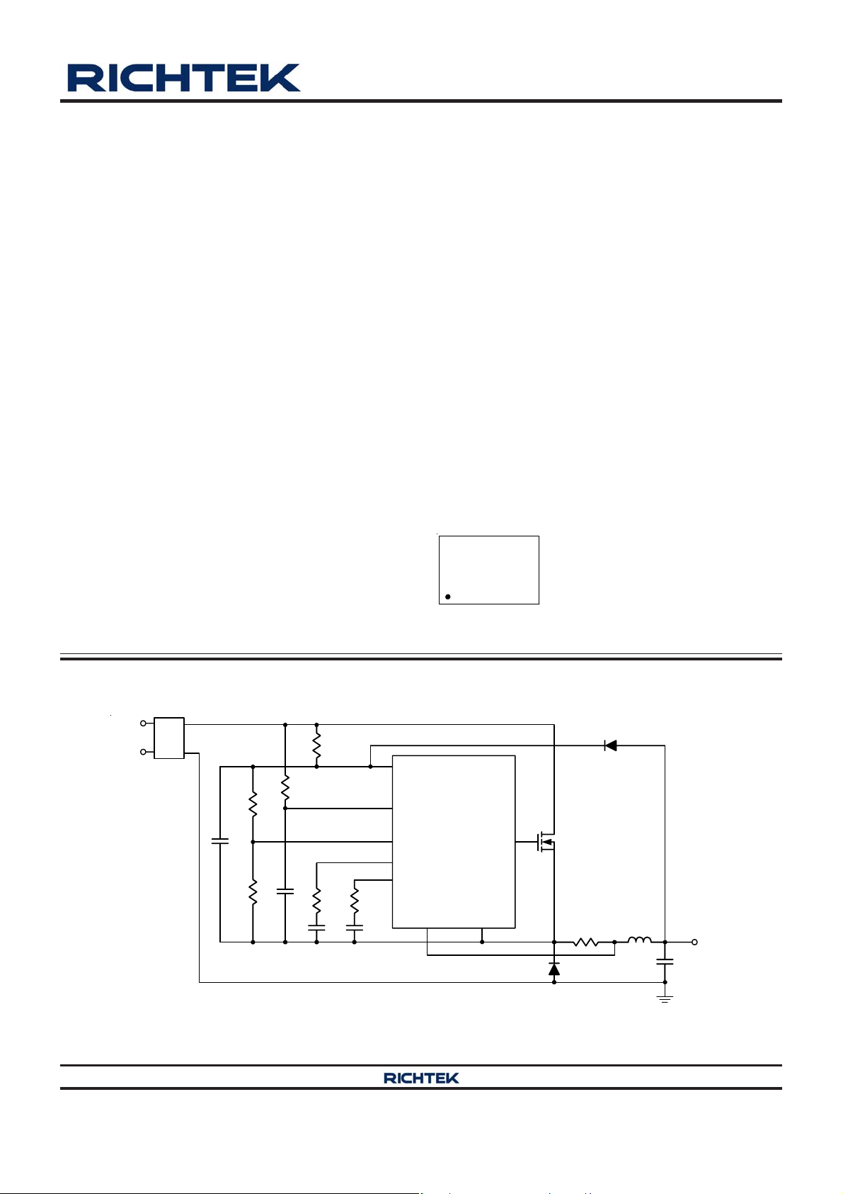
Simplified Application Circuit
AC IN
Copyright 2013 Richtek Technology Corporation. All rights reserved. is a registered trademark of Richtek Technology Corporation.
©
+
~
-
C2
R2
R3
R1
C3
Rstart
R4
C4
R5
C5
VCC
SIN
FB
ICOMP
VCOMP
RT8461
GNDSENSE
GATE
M1
DS8461-01 March 2013 www.richtek.com
D2
RS
D1
L
C1
V
OUT
1
RT8461
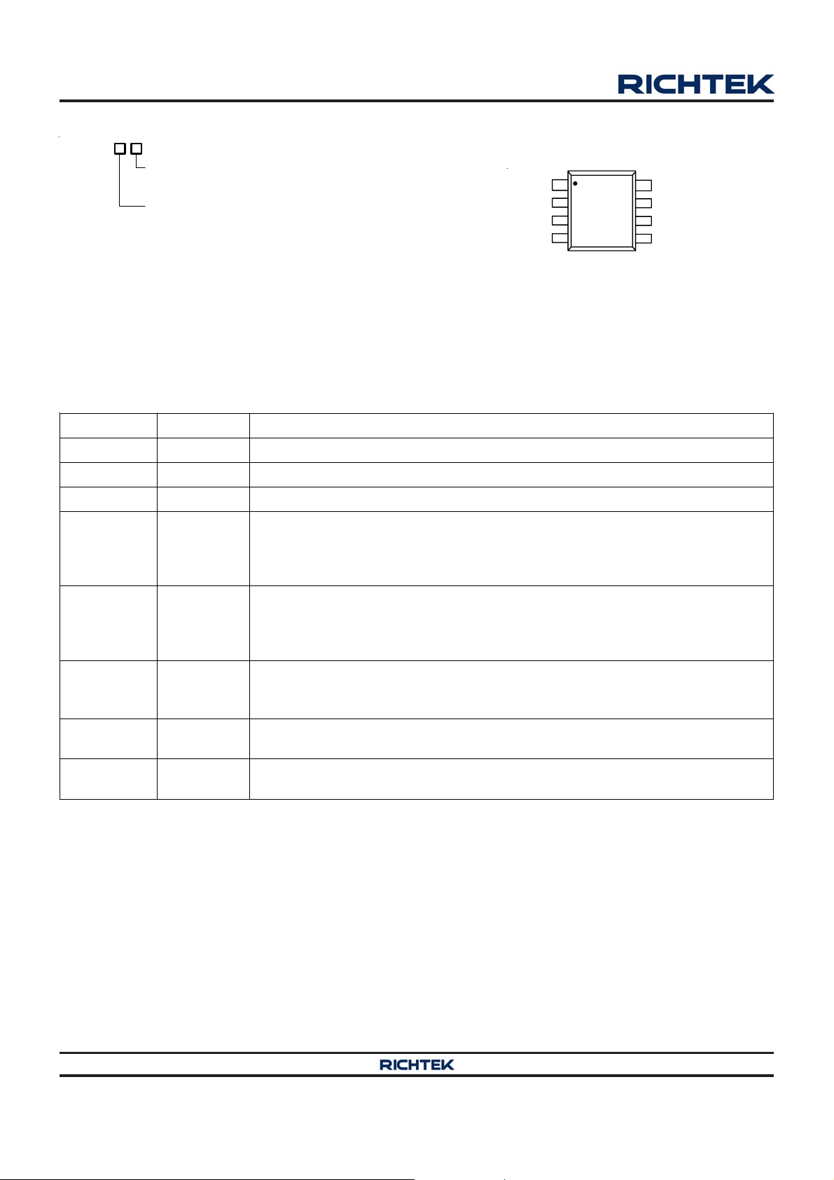
Ordering Information
Pin Configurations
RT8461
Package Type
S : SOP-8
Lead Plating System
Z : ECO (Ecological Element with
Halogen Free and Pb free)
Note :
Richtek products are :
` RoHS compliant and compatible with the current require-
ments of IPC/JEDEC J-STD-020.
` Suitable for use in SnPb or Pb-free soldering processes.
Functional Pin Description
Pin No. Pin Name Pin Function
1 GND Ground.
2 GATE Gate Driver for External MOSFET Switch.
3 VCC Power Supply. For good bypass, place a ceramic capacitor near the VCC pin.
Inductor Current Sense. The inductor current is sensed by a resistor between GND
4 SENSE
and SENSE pins. The sense pin signal is used as the saw tooth signal to the PWM
comparator. The comparator output will modulate the GATE turn-on duty to
achieve the output voltage regulation.
GND
GATE
VCC
SENSE
(TOP VIEW)
8
2
3
4
7
6
5
SOP-8
VCOMP
SIN
ICOMP
FB
5 FB
6 ICOMP
7 SIN
8 VCOMP
Output Voltage Sense. The Output voltage is sensed through an external resistor
divider. The sensed voltage (which is tied to amplifier negative input) is compared
to an internal reference threshold at 1.2V (which is tied to amplifier positive input).
The output of this GM amplifier is the VCOMP pin.
Output of this Multiplier. To achieve high power factor, the voltage loop amplifier
output signal is modulated with the sensed input voltage through the SIN pin by an
internal multiplier. A compensation capacitor between ICOMP and GN D is needed.
Input Power Voltage Sensing for PFC Function. An external resistor for input
voltage sensing is connected to the power input.
Output of the Internal Voltage Loop GM Amplifier. A compensation network
between VCOMP and GND is needed.
Copyright 2013 Richtek Technology Corporation. All rights reserved. is a registered trademark of Richtek Technology Corporation.
2
©
DS8461-01 March 2013www.richtek.com
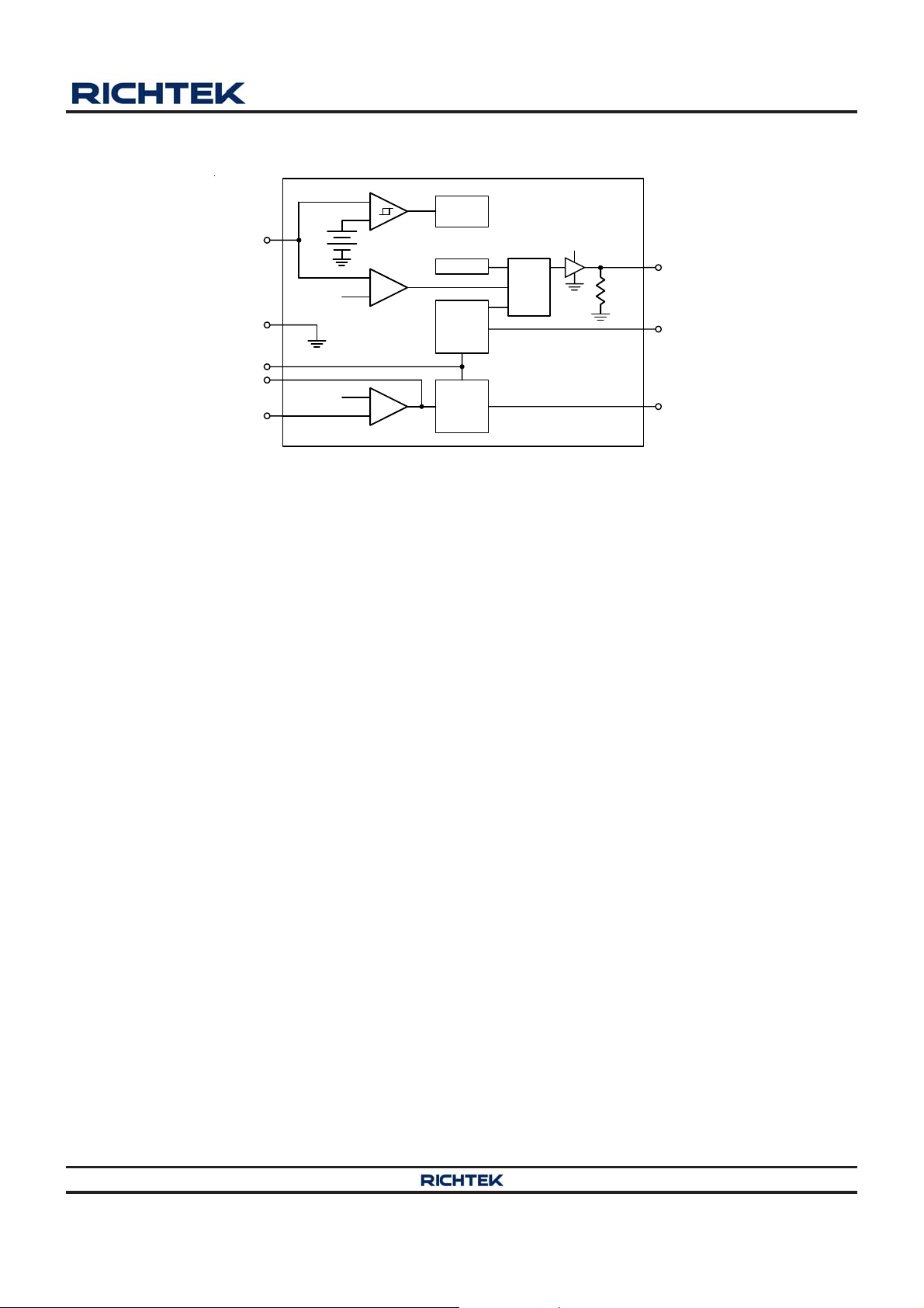
Function Block Diagram
RT8461
+
-
+
VCC
35V
GND
ICOMP
VCOMP
1.2V
FB
16V/8V
OVP
+
-
+
-
Operation
The RT8461 is a floating-GND Buck PWM current mode
controller with an integrated low side floating gate driver .
The start up voltage of RT8461 is around 10V . Once VCC
is above 16V, the RT8461 will maintain operation until
VCC drops below 8V .
The RT8461's main control loop consists of a 47kHz fixed
frequency oscillator, a n internal 1.2V feedback (FB) voltage
sense threshold, and the PFC control circuit with a PWM
comparator. In normal operation, the GATE turns high
when the gate driver is set by the oscillator (OSC). When
the feedback (FB) voltage is below the reference 1.2V
Chip
Enable
12V
OSC
PWM
Control
Circuit
PFC
Control
Circuit
S Q
R
R
200k
GATE
SENSE
SIN
threshold, the VCOMP pin voltage will go high. The ICOMP
signal is the result of VCOMP signal multiplied with SIN
signal. Higher ICOMP voltage mean s longer G ATE turnon period. The GATE does not always turn-off in each
cycle. The G ATE will be turned on again by OSC for the
next switching cycle.
The RT8461 provides several fault protections, including
input voltage Under V oltage Lockout (UVLO), Over Current
Protection (OCP) and VCC Over V oltage Protection (OVP).
Additionally , to ensure the system reli ability, the RT8461
is built with internal thermal protection function.
Copyright 2013 Richtek Technology Corporation. All rights reserved. is a registered trademark of Richtek Technology Corporation.
DS8461-01 March 2013 www.richtek.com
©
3
RT8461
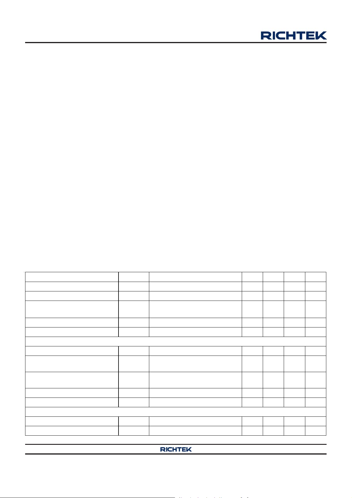
Absolute Maximum Ratings (Note 1)
z Supply V oltage, VCC----------------------------------------------------------------------------------------------------- −0.3V to 40V
z SIN ---------------------------------------------------------------------------------------------------------------------------- −0.3V to 40V
z GA TE (Note 6) ----------------------------------------------------------------------------------------------------------- −0.3V to 16V
z VCOMP , ICMOP----------------------------------------------------------------------------------------------------------- −0.3V to 3.5V
z FB----------------------------------------------------------------------------------------------------------------------------- −0.3V to 2V
z SENSE ---------------------------------------------------------------------------------------------------------------------- −1V to 0.3V
z Power Dissipation, P
SOP-8------------------------------------------------------------------------------------------------------------------------ 0.53W
z Package Thermal Re sistance (Note 2)
SOP-8, θJA------------------------------------------------------------------------------------------------------------------ 188 °C/W
z Junction T emperature----------------------------------------------------------------------------------------------------- 150°C
z Lead Temperature (Soldering, 10 sec.)------------------------------------------------------------------------------- 260°C
z Storage T emperature Range -------------------------------------------------------------------------------------------- −65°C to 150°C
z ESD Susceptibility (Note 3)
HBM (Human Body Model)---------------------------------------------------------------------------------------------- 2kV
MM (Machine Model) ----------------------------------------------------------------------------------------------------- 200V
@ T
D
= 25°C
A
Recommended Operating Conditions
z Supply V oltage VCC------------------------------------------------------------------------------------------------------ 16V to 33V
z Junction T emperature Range-------------------------------------------------------------------------------------------- −40°C to 125°C
z Ambient T emperature Range-------------------------------------------------------------------------------------------- −40°C to 85°C
(Note 4)
Electrical Characteristics
(VCC = 24VDC, C
Inpu t Start- Up Vol tage VST 16 17 18 V
Under Voltage Lockout Threshold V
Under Voltage Lockout Threshold
Hysteresis
Inpu t Supply Curre nt ICC After Start-Up, VCC = 24V -- 2 5 mA
Inpu t Quiesc ent Current IQC Before Start-Up, VCC = 7V -- 0.1 -- μA
Oscillator
Switching Frequency fSW V
Maximum Duty in Transient
Operation
Maximum Duty in Steady State
Operation
Blanking Time t
Mini mum T urn- Off Time (Note 5) -- 650 -- n s
Current Sense Amplifier
Current Sense Voltage V
Sense Input Current I
Copyright 2013 Richtek Technology Corporation. All rights reserved. is a registered trademark of Richtek Technology Corporation.
4
©
LOAD
= 1nF, R
= 2.2Ω in series, TA = 25°C, unless otherwise specified)
LOAD
Parameter Symbol Test Conditions Min Typ Max Unit
7 8 11 V
UVLO
ΔV
D
D
BLANK
SENSE
-- 2 4 V
UVLO
= 14V 38 47 52 kHz
SIN
MAX(TR)
MAX
VC = 3V -- -- 100 %
(Note 5) -- 97 -- %
-- 300 -- ns
SENSE
V
= 1V, SIN = 15V -- −100 -- mV
COMP
Sense = 100mV (Note 5) -- 10 -- μA
DS8461-01 March 2013www.richtek.com

RT8461
Parameter Symbol Test Conditions Min Typ Max Unit
Gate Driver Output
GATE Pin Maximum Voltage V
High V
GATE Voltage
Low V
GATE Drive Rise and Fall Time 1nF Load at GATE -- 10 50 ns
GATE Drive Source and Sink
Peak Current
PFC Contro l
SIN Pin In put Current V
ICOMP Threshold for PWM
Switch Off
VC Output Current I
Feedb ack Voltage VFB 1.1 1.2 1.3 V
Feedb ack Input Current IFB V
OVP
Over Voltage Protection V
Thermal Protection
Thermal Shutdown Temperature TSD 150 -- -- °C
SIN Pin Input Resistance -- 250 -- kΩ
No Load at GATE Pin 11.8 12.5 16 V
GATE
I
= −20mA -- 12.1 --
GATE
GATE_H
GATE_L
I
= −100μA -- 12.4 --
GATE
I
= 20mA -- 0.75 --
GATE
I
= 100μA -- 0.5 --
GATE
V
V
1nF Load at GATE (Note 4) -- 0.5 0.8 A
= 14V 50 60 70 μA
SIN
V
VCOMP
-- 1.2 -- V
ICOMP
0.5V ≤ VC ≤ 2.4V (Note 5) -- 16 -- μA
= 1.2V (Note 5) -- 1 -- μA
FB
VCC Pin 32 35 38 V
OVP
Note 1. Stresses beyond those listed “Absolute Maximum Ratings” may cause permanent damage to the device. These are
stress ratings only, and functional operation of the device at these or any other conditions beyond those indicated in
the operational sections of the specifications is not implied. Exposure to absolute maximum rating conditions may
affect device reliability.
Note 2. θ
Note 3. Devices are ESD sensitive. Handling precaution is recommended.
Note 4. The device is not guaranteed to function outside its operating conditions.
Note 5. Guaranteed by design; not subject to production test.
Note 6. The GATE voltage is internally clamped and varies with operating conditions.
is measured at T
JA
= 25°C on a high effective thermal conductivity four-layer test board per JEDEC 51-7.
A
Copyright 2013 Richtek Technology Corporation. All rights reserved. is a registered trademark of Richtek Technology Corporation.
DS8461-01 March 2013 www.richtek.com
©
5

RT8461
Typical Application Circuit
AC IN
+
~
-
C2
R2
R3
R1
2M
C3
100p
Rstart
1.5M
R4
C4
R5
C5
3
VCC
7
SIN
5
FB
6
ICOMP
8
VCOMP
RT8461
4
GATE
GNDSENSE
D1
2
M1
1
RS
D2
L
C1
V
OUT
Copyright 2013 Richtek Technology Corporation. All rights reserved. is a registered trademark of Richtek Technology Corporation.
©
DS8461-01 March 2013www.richtek.com
6

)
Typical Operating Characteristics
)
RT8461
Supply Current vs. Input Voltage
2.0
1.9
1.8
1.7
1.6
Supply Current (mA
1.5
1.4
8 1318232833
Input Voltage (V)
V
vs. Temperature
40
38
36
(V)
OVP
V
34
OVP
Supply Current vs. Tempe rature
2.5
2.0
1.5
1.0
Supply Current (mA
0.5
0.0
-50 -25 0 25 50 75 100 125
V
Temperatur e (°C)
UVLO vs. Temperature
20
17
UVLO-H
14
11
UVLO (V)
CC
= 24V
32
30
-50-25 0 25 50 75100125
Temperatur e (°C)
FB Voltage vs. Temperature
1.30
1.25
1.20
FB Volt age (V)
1.15
V
1.10
-50 -25 0 25 50 75 100 125
Temperature (°C)
CC
= 24V
8
5
-50 -25 0 25 50 75 100 125
UVLO-L
Temperatur e (°C)
GATE Voltage High vs. Temperature
13.5
13.2
I
= −100μA
GATE
12.9
12.6
12.3
GATE Volt age (V)
12.0
11.7
-50 -25 0 25 50 75 100 125
I
= −20mA
GATE
Temperatur e (°C)
V
= 24V
CC
Copyright 2013 Richtek Technology Corporation. All rights reserved. is a registered trademark of Richtek Technology Corporation.
©
DS8461-01 March 2013 www.richtek.com
7

RT8461
GATE Voltage Low vs. Te m pe rature
1.0
I
= 20mA
0.8
0.6
0.4
GATE
I
GATE
= 100μA
GATE Volt age (V)
0.2
V
= 24V
0.0
-50-25 0 25 50 75100125
CC
Temperatur e (°C)
Minimum On-Time vs. Temperature
350
330
310
290
Minimum On-Time (ns) 1
270
V
= 24V
250
-50 -25 0 25 50 7 5 100 125
Temperature (°C)
CC
Switching Frequency vs. Temperature
45
43
41
39
37
Switching Frequency (kHz) 1
V
= 24V
35
-50 -25 0 25 50 75 100 125
CC
Temperatur e (°C)
ICOM P Voltage vs. SIN Vo ltage
3.5
3.0
2.5
V
= 2V
COMP
V
= 1.5V
(V)
COMP
V
COMP
V
COMP
V
COMP
= 1V
= 0.7V
= 0.5V
V
CC
= 24V
2.0
(V)
1.5
ICOMP
V
1.0
0.5
0.0
02468
V
SIN
SIN Cur re nt vs. Input Voltage
110
V
= 14V
V
SIN
SIN
= 28V
V
= 24V
CC
100
90
80
70
SIN Current (µA)
60
50
8 1318232833
0.2
0.0
-0.2
Threshold (V)
-0.4
SENSE
V
-0.6
-0.8
V
-50 -25 0 25 50 75 100 125
Input Voltage (V)
Copyright 2013 Richtek Technology Corporation. All rights reserved. is a registered trademark of Richtek Technology Corporation.
©
Threshold vs. Temperature
SENSE
V
= 1V
SIN
V
= 10V
SIN
V
= 20V
SIN
V
CC
Temperature (°C)
= 24V, V
COMP
DS8461-01 March 2013www.richtek.com
8
= 3V

Application Information
)
RT8461
The RT8461 provides active power factor correction for
universal off-line power systems with fewer external
components.
It is suitable for wide line input ra nge a pplications from 85
to 265 V AC. The RT8461 ca n operate in both Continuous
Conduction Mode (CCM) and Discontinuous Conduction
Mode (DCM) by fixed frequency PWM control. The fixed
switching frequency is internally set at 47kHz.
The IC operates with a dual control topology; the inner
current loop and the outer voltage loop. The inner current
loop of the IC controls the sinusoidal profile for the average
input current. It uses the dependency of the PWM duty
cycle on the line input voltage to determine the
corresponding input current. This mea ns the average input
current follows the input voltage as long as the device
operates in CCM. Under light load condition, depending
on the choke inductance, the system may enter into DCM.
In DCM, the average current waveform will be distorted
but the resultant harmonics are still low enough to meet
the standard of IEC61000-3-2.
The RT8461 employs average current control to achieve a
better input current waveform.
achieve high power factor and good THD, the multiplier
transfer character is designed to be linear over a wide
dyna mic range, na mely , 1V to 3V f or SIN a nd 0.8V to 1.2V
for FB. The relationship between the multi plier output and
inputs is described a s the below equation :
V = kV 0.7V
ICOMP COMP SIN
where V
the multiplier gain, V
and V
I
AC
+
+
V
AC
~
-
-
×−×
(
is the reference for the current sense, k is
ICOMP
is the error amplif ier output voltage
COMP
is the sinusoidal reference voltage on pin 7.
SIN
I
IN
V
M1
IN
GATE
+
-
SENSE
47kHz
R
D1
I
L
L
S
C1
I
OUT
+
V
OUT
-
1
SIN
Multiplier
VCOMP
R5
C5
+
V
REF
Voltage
Error Amplifier
FB
Sinusoidal
Reference
K
S
ICOMP
R2
R3
In Figure 1, the inductor current is sensed and filtered by
a current error amplifier which output drives a PWM
modulator. In this way, the inner current loop tends to
minimize the error between the average input current I
and its reference. The converter works in CCM, so the
same con siderations done with regard to the peak current
control can be a pplied.
Multiplier
The multiplier has two inputs. The SIN pin is the divided
sinusoidal voltage which makes the current sense
comparator threshold voltage vary from zero to peak value.
The other input is the output of error a mplifier at VCOMP
pin. In this way, the input average current wave will be
sinusoidal as well as reflects the load status. In order to
Figure 1. Functional Block with PFC CCM Control
Pulse Width Modulator
IN
The IC employs an average current control scheme in CCM
to achieve the power fa ctor correction. If the voltage loop
is working and output voltage is kept constant, the duty
cycle, DON, for a CCM PFC system is given as
V
D =
ON
OUT
V
IN
From the above equation, DON is relative to VIN. The
objective of the current loop is to regulate the average
inductor current such that it is relative to the duty cycle,
DON, and the input voltage, VIN. Figure 2 shows the
waveform for the control scheme.
Copyright 2013 Richtek Technology Corporation. All rights reserved. is a registered trademark of Richtek Technology Corporation.
DS8461-01 March 2013 www.richtek.com
©
9

RT8461
Ramp Profile
GATE
Drive
I
L
I
OUT, AVG
t
Figure 2. A verage Current Controls in CCM
The PWM is performed by the intersection of a ra mp signal
with the current error amplifier output. The PWM cycle
starts with the GATE turns on for a minimum duration
about 300ns typical. In ca se of the inductor current reaches
the in peak current limitation, the GATE will be turned off
immediately when V
is triggered.
SENSE
Error Amplifier
The outer voltage loop of the cascaded control scheme
regulates the PFC output bus voltage V
. The error
OUT
amplifier's inverting feedback FB is connected to an
external resistor divider which senses the output voltage.
The output of the error amplif ier is one of the two inputs of
the multiplier . A compensation loop is connected outside
between the error amplif ier output at the VCOMP pin, an d
ground of the GND pin. Normally , the compensation loop
bandwidth is very low to realize high power fa ctor for PFC
converter. The compen sation is also responsible for the
soft-start function which controls an increasing AC input
current during start-up.
FB
R3
⎛⎞
⎜⎟
R2 + R3
⎝⎠
VCOMP
×
V
OUT
R5
C5
+
1.2V
Current Sense/Current Sense Comparator
The PFC switch's turn-on current is sensed through an
external resistor in series with the switch. When the
sensed voltage exceeds the threshold voltage (the
multiplier output), the current sense comparator will
become low and the external MOSFET will be turned off.
This insures a cycle-by-cycle current mode control
operation. The max value usually occurs in start-up
process or abnormal conditions such as short load.
Output Gate Driver
The output gate driver is a fast totem pole gate drive. It
has a built-in cross conduction current protection and a
Zener diode to protect the external transistor switch
against unexpected over voltages.
The maximum voltage at GATE is typically clamped at
12.5V.
Under Voltage Lockout (UVLO)
The RT8461 internal UVLO block monitors the VCC power
supply with 2V hysteresis. The hysteresis behavior
guarantees a one-short startup resistor and hold-up
cap acitor . The IC will then be con suming typically 150μA
when start-up and the power dissipation on resistor would
be less than 0.1W . After start-up, the operating current is
typically 1.65mA to get a better efficiency.
Over Voltage Protection (OVP)
Whenever V
exceeds the rated value by 5%, the over
OUT
voltage protection is activated. This is implemented by
sensing the voltage at FB pin with respect to a reference
voltage of 1.25V. A FB voltage higher than 1.25V will
immediately reduce the output duty cycle a nd bypass the
normal voltage loop control. This results in a lower input
power to reduce the output voltage V
V
CC
10V
OUT
.
8V
Figure 3. V oltage Loop Amplifier
IC's
State
OFF
Start UpNormal
Operation
Open Loop/
Standby
Normal
Operation
Figure 4. State of Power VCC Operation
Copyright 2013 Richtek Technology Corporation. All rights reserved. is a registered trademark of Richtek Technology Corporation.
10
©
DS8461-01 March 2013www.richtek.com
t
OFF

RT8461
Thermal Considerations
For continuous operation, do not exceed absolute
maximum junction temperature. The maximum power
dissipation depends on the thermal resistance of the IC
package, PCB layout, rate of surrounding airflow, and
difference between junction and a mbient temperature. The
maximum power dissipation can be calculated by the
following formula :
P
where T
the ambient temperature, a nd θ
D(MAX)
= (T
J(MAX)
− TA) / θ
J(MAX)
JA
is the maximum junction temperature, T
is the junction to ambient
JA
A
thermal resistance.
For recommended operating condition specifications, the
maximum junction temperature is 125°C. The junction to
a mbient thermal resistance, θJA, is layout dependent. For
SOP-8 package, the thermal resista nce, θJA, is 188°C/W
on a standard JEDEC 51-7 four-layer thermal test board.
The maximum power dissipation at TA = 25°C can be
calculated by the following formula :
Layout Consideration
R
start
VCC
SIN
D1
C1
D2
is
PGND
C2
-
AC IN
+
R1
C3
RS
L
GND
GATE
M1
GND
GATE
VCC
SENSE
Locate the input capacitor as
close to VCC pin as possible
Locate the compensation components
to VCOMP pin as close as possible
2
3
4
Figure 6. PCB Layout Guide
GND
8
VCOMP
7
SIN
6
ICOMP
5
FB
VCC
R2
R5
R4
R3
C5
C4
GND
P
= (125°C − 25°C) / (188°C/W) = 0.53W for
D(MAX)
SOP-8 package
The maximum power dissipation depends on the operating
ambient temperature for fixed T
and thermal
J(MAX)
resistance, θJA. The derating curve in Figure 5 allows the
designer to see the effect of rising ambient temperature
on the maximum power dissipation.
0.6
0.5
0.4
0.3
0.2
0.1
Maximum Power Dissipation (W) 1
0.0
0 25 50 75 100 125
Ambient Tempera ture (°C )
Four-Layer PCB
Figure 5. Derating Curve of Maxi mum Power Dissi pation
Copyright 2013 Richtek Technology Corporation. All rights reserved. is a registered trademark of Richtek Technology Corporation.
DS8461-01 March 2013 www.richtek.com
©
11

RT8461
Outline Dimension
A
J
I
B
F
C
D
H
M
Dimensions In Millimeters Dimensions In Inches
Symbol
Min Max Min Max
A 4.801 5.004 0.189 0.197
B 3.810 3.988 0.150 0.157
C 1.346 1.753 0.053 0.069
D 0.330 0.508 0.013 0.020
F 1.194 1.346 0.047 0.053
H 0.170 0.254 0.007 0.010
I 0.050 0.254 0.002 0.010
J 5.791 6.200 0.228 0.244
M 0.400 1.270 0.016 0.050
Richtek Technology Corporation
5F, No. 20, Taiyuen Street, Chupei City
Hsinchu, Taiwan, R.O.C.
Tel: (8863)5526789
8-Lead SOP Plastic Package
Richtek products are sold by description only. Richtek reserves the right to change the circuitry and/or specifications without notice at any time. Customers should
obtain the latest relevant information and data sheets before placing orders and should verify that such information is current and complete. Richtek cannot
assume responsibility for use of any circuitry other than circuitry entirely embodied in a Richtek product. Information furnished by Richtek is believed to be
accurate and reliable. However, no responsibility is assumed by Richtek or its subsidiaries for its use; nor for any infringements of patents or other rights of third
parties which may result from its use. No license is granted by implication or otherwise under any patent or patent rights of Richtek or its subsidiaries.
DS8461-01 March 2013www.richtek.com
12

 Loading...