


®
5A, 24V, 570kHz Step-Down Converter
RT8251
General Description
The RT8251 is a monolithic step-down switch mode
converter with a built-in internal power MOSFET . It a chieves
5A continuous output current over a wide input supply
range with excellent load a nd line regulation. Current mode
operation provides fast tra nsient response a nd ea ses loop
stabilization.
The RT8251 provides protection functions such as
cycle-by-cycle current limiting and thermal shutdown. In
shutdown mode, the regulator draws 25μA of supply
current. Programmable soft-start minimizes the inrush
supply current and the output overshoot at initial startup.
The RT8251 requires a minimum number of external
components. The RT8251 is available in WQ F N-16L 3x3
and SOP-8 (Exposed Pad) pa ckages.
Pin Configurations
(TOP VIEW)
Features
zz
Wide Operating Input Voltage Range : 4.75V to 24V
z
zz
zz
z Adjustable Output Voltage Range : 0.8V to 15V
zz
zz
z Output Current up to 5A
zz
μμ
zz
z 25
μA Low Shutdown Current
zz
μμ
zz
z Internal Power MOSFET : 70m
zz
zz
z High Efficiency up to 95%
zz
zz
z 570kHz Fixed Switching Frequency
zz
zz
z Stable with Low ESR Output Ceramic Capacitors
zz
zz
z Thermal Shutdown Protection
zz
zz
z Cycle-By-Cycle Over Current Protection
zz
zz
z RoHS Compliant and Halogen Free
zz
ΩΩ
Ω
ΩΩ
Applications
z Distributed Power Systems
z Battery Charger
z DSL Modems
z Pre-regulator for Linear Regulators
VIN
VINSWSW
VIN
1
2
VIN
VIN
GND
GND
3
4
FB
COMP
WQFN-16L 3x3
BOOT
VIN
SW
GND
2
GND
3
4
SOP-8 (Exposed Pad)
17
EN
13141516
SW
12
11
SW
10
SW
BOOT
9
8765
SS
Ordering Information
RT8251
Package Type
QW : WQFN-16L 3x3 (W-Type)
SP : SOP-8 (Exposed Pad-Option 1)
Lead Plating System
G : Green (Halogen Free and Pb Free)
Note :
Richtek products are :
` RoHS compliant and compatible with the current require-
8
SS
7
EN
6
9
COMP
5
FB
ments of IPC/JEDEC J-STD-020.
` Suitable for use in SnPb or Pb-free soldering processes.
Copyright 2013 Richtek Technology Corporation. All rights reserved. is a registered trademark of Richtek Technology Corporation.
©
DS8251-04 February 2013 www.richtek.com
1

RT8251
Marking Information
RT8251GQW
GE= : Product Code
GE=YM
DNN
Typical Application Circuit
YMDNN : Date Code
RT8251GSP
RT8251
GSPYMDNN
RT8251GSP : Product Number
YMDNN : Date Code
4.75V to 24V
V
Chip Enable
4.75V to 24V
Chip Enable
IN
C
10µF x 2
C
SS
10nF
Exposed Pad (17)
V
IN
C
SS
10nF
Exposed Pad(9)
1, 2, 3,
15, 16
IN
VIN
RT8251
7
EN
8
SS
4,
GND
BOOT
SW
FB
COMP
9
10 to 14
5
2.2nF
6
C
C
(Open)
C
C
100nF
D
B540C
R
22k
P
BOOT
C
L
4.7µH
Figure 1. T ypical Application Circuit for WQFN-16L 3x3
C
IN
10µF x 2
2
VIN
RT8251
7
EN
8
SS
4,
GND
BOOT
SW
FB
COMP
1
C
BOOT
100nF
3
D
B540C
5
C
C
2.2nF
6
4.7µH
R
C
22k
L
R1
30.9k
R2
10k
R1
30.9k
R2
10k
C
OUT
22µF x 2
V
3.3V/5A
C
OUT
22µF x 2
V
OUT
3.3V/5A
OUT
C
P
NC
Figure 2. T ypical Application Circuit for SOP-8 (Exposed Pa d)
Table 1. Recommended Component Selection
V
(V) R1 (kΩ) R2 (kΩ) RC (kΩ) CC (nF) L1 (μH) C
OUT
OUT
(μF)
15 182 10 51 1 22 44
10 115 10 43 1.2 10 44
8 91 10 39 1.5 10 44
5 52.3 10 30 1.5 6.8 44
3.3 30.9 10 22 2.2 4.7 44
2.5 21.5 10 16 2.2 4.7 44
1.8 12.4 10 13 2.2 2.2 44
1.2 4.99 10 13 2.2 2.2 44
Copyright 2013 Richtek Technology Corporation. All rights reserved. is a registered trademark of Richtek Technology Corporation.
2
©
DS8251-04 February 2013www.richtek.com

Functional Pin Description
Pin No.
WQFN-16L 3x3
1, 2, 3, 15, 16 2 VIN
4,
17 (Exposed Pad )
5 5 FB
6 6 COMP
7 7 EN
8 8 SS
9 1 BOOT
10, 11, 12, 13,
14
SOP-8
(Exposed Pad)
4,
9 (Exposed Pad)
3 SW
Pin Name Pin Function
GND
RT8251
Power Input. VIN supplies the power to the IC, as well as the
step-down converter switches. Connect VIN with a 4.75V to 24V
power source. Connect VIN to GND with a capacitor that the
capacitance is large enough to eliminate noise on the input to the
IC.
Ground. This pin is the voltage reference for the regulated output
voltage. For this reason, care must be taken in its layout. This
node should be placed outside of the D1 to C
prevent switching current spikes from inducing voltage noise into
the part. The exposed pad must be soldered to a large PCB and
connected to GND for maximum power dissipation.
Feedback Input. An external resistor divider from the output to
GND, tapped to the FB pin, sets the output voltage.
Compensation Node. This node is the output of the
transconductance error amplifier and the input to the current
comparator. Frequency compensation is done at this node by
connecting a series R-C to ground.
Enable Input. EN is a digital input that turns the regulator on or
off. Drive EN higher than 1.4V to turn on the regulator, lower
than 0.4V to turn it off. For automatic startup, leave EN
unconnected.
Soft-Start Control Input. SS controls the soft start period.
Connect a capacitor (≧ 10nF) from SS to GND to set the
soft-start period. A 10nF capacitor sets the Soft-Start period to
1ms.
Bootstrap. This capacitor C
switch’s gate above the supply voltage. It is connected between
the SW and BS pins to form a floating supply across the power
switch driver. The voltage across C
supplied by the internal +5V supply when the SW pin voltage is
low.
Power Switching Output. SW is the switching node that supplies
power to the output. Connect the output LC filter from SW to the
output load. Note that a capacitor is required from SW to BOOT
to power the high-side switch.
is needed to drive the power
BOOT
BOOT
ground path to
IN
is about 5V and is
Copyright 2013 Richtek Technology Corporation. All rights reserved. is a registered trademark of Richtek Technology Corporation.
DS8251-04 February 2013 www.richtek.com
©
3
RT8251
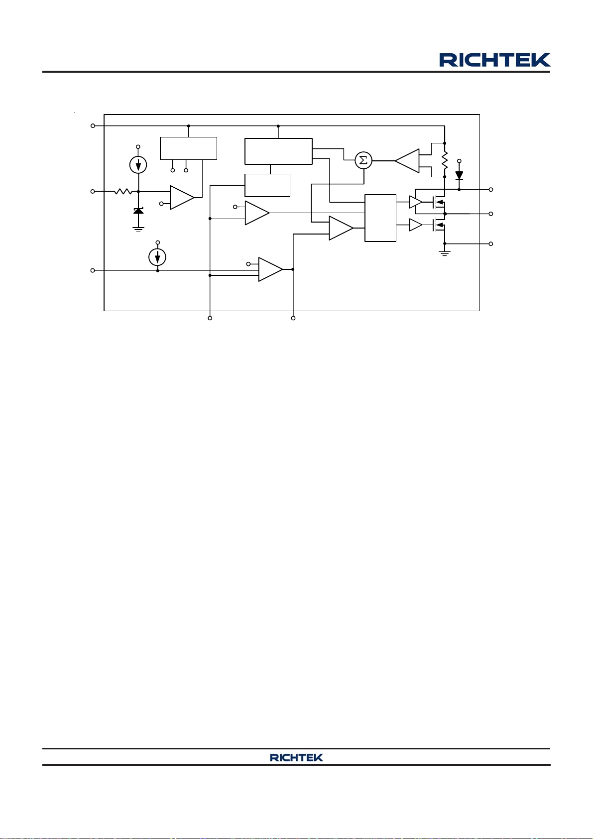
Function Block Diagram
VIN
EN
SS
1µA
10k
3V
V
CC
1.1V
Regulator
VA
-
+
Shutdown
Comparator
V
CC
10µA
Internal
V
CC
0.4V
Comparator
0.8V
Gm = 820µA/V
FB
Oscillator
570kHz
Foldback
Control
+
-
UV
+
EA
+
-
COMP
Slope Comp
+
Current
Comparator
Current Sense
Amplifier
Logic
+
-
VA
Absolute Maximum Ratings (Note 1)
z Supply Voltage, V
z Switching Voltage, V
z BOOT V oltage, V
z All Other Pins -------------------------------------------------------------------------------------------------−0.3V to 6V
z Power Dissipation, P
WQFN-16L 3x3 -----------------------------------------------------------------------------------------------1.471W
SOP-8 (Exposed Pad) --------------------------------------------------------------------------------------1.333W
z Package Thermal Re sistance (Note 2)
WQF N-16L 3x3, θJA------------------------------------------------------------------------------------------68°C/W
WQFN-16L 3x3, θJC-----------------------------------------------------------------------------------------7.5°C/W
SOP-8 (Exposed pad), θJA---------------------------------------------------------------------------------75°C/W
SOP-8 (Exposed Pad), θJC--------------------------------------------------------------------------------15°C/W
z Junction T emperature----------------------------------------------------------------------------------------150°C
z Lead T e mperature (Soldering, 10 sec.)------------------------------------------------------------------260 °C
z Storage T emperature Range -------------------------------------------------------------------------------−65°C to 150°C
z ESD Susceptibility (Note 3)
HBM (Human Body Model)---------------------------------------------------------------------------------2kV
------------------------------------------------------------------------------------------−0.3V to 26V
IN
-------------------------------------------------------------------------------------−0.3V to (VIN + 0.3V)
SW
---------------------------------------------------------------------------------------(V
BOOT
@ TA = 25°C
D
− 0.3V) to (V
SW
BOOT
SW
GND
SW
+ 6V)
Recommended Operating Conditions (Note 4)
z Supply Voltage, V
z Enable Voltage, V
z Junction T emperature Range-------------------------------------------------------------------------------−40°C to 125°C
z Ambient T emperature Range-------------------------------------------------------------------------------−40°C to 85°C
Copyright 2013 Richtek Technology Corporation. All rights reserved. is a registered trademark of Richtek Technology Corporation.
©
4
------------------------------------------------------------------------------------------4.75V to 24V
IN
-----------------------------------------------------------------------------------------0V to 5.5V
EN
DS8251-04 February 2013www.richtek.com

RT8251
Electrical Characteristics
(VIN = 12V, TA = 25°C unless otherwise specified)
Parameter Symbol Test Conditions Min Typ Max Unit
Feedb ack Ref eren ce V olt age VFB 4.75V ≦ VIN ≦ 24V 0.784 0.8 0.816 V
High-Side Switch-On Resistance R
Low -Side Swi tch -On Res is tanc e R
DS(ON)1
DS(ON)2
High-Side Switch Leakage V
Current Limit I
LIM
Current Sense Transconductance GCS Output Current to V
Erro r Amplifi er T ansc onduct ance gm ΔIC = ±10μA -- 920 -- μA/V
Oscillator Frequency fSW 420 570 720 kHz
Short Circuit Oscillation Frequency V
Maximum Duty Cycle D
MAX
Mini mum On- Ti me tON -- 100 -- ns
UVLO Threshold Rising -- 4.1 -- V
UVL O Thresh old Hyst eresis -- 200 -- mV
Logic Low VIL -- -- 0.4
EN Input Voltage
Logic High V
IH
Enable Pu l l Up Cu r r en t V
Shutdown Current I
SHDN
Quies cen t Curr ent IQ V
Soft-Start Current ISS V
Soft-Start Period C
Thermal Shutdown TSD -- 150 -- °C
Note 1. Stresses beyond those listed “Absolute Maximum Ratings” may cause permanent damage to the device. These are
stress ratings only, and functional operation of the device at these or any other conditions beyond those indicated in
the operational sections of the specifications is not implied. Exposure to absolute maximum rating conditions may
affect device reliability.
Note 2. θ
Note 3. Devices are ESD sensitive. Handling precaution is recommended.
Note 4. The device is not guaranteed to function outside its operating conditions.
is measured at T
JA
measured at the exposed pad of the package.
= 25°C on a high effective thermal conductivity four-layer test board per JEDEC 51-7. θJC is
A
-- 70 -- mΩ
-- 15 -- Ω
= 0V, V
EN
Duty = 85%; V
= 0V -- 185 -- kHz
FB
V
= 0.7V -- 85 -- %
FB
= 0V -- -- 10 μA
SW
BOOT−SW
= 4.8V -- 6.8 -- A
-- 4.6 -- A/V
COMP
1.4 -- 5.5
= 0V -- 1 -- μA
EN
VEN = 0V -- 25 -- μA
= 2V, VFB = 1V -- 0.8 1 mA
EN
= 0V -- 10 -- μA
SS
= 10nF -- 1 -- ms
SS
V
Copyright 2013 Richtek Technology Corporation. All rights reserved. is a registered trademark of Richtek Technology Corporation.
DS8251-04 February 2013 www.richtek.com
©
5
RT8251
)
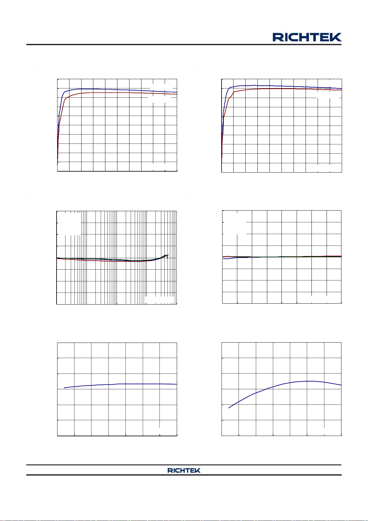
Typical Operating Characteristics
Efficiency vs. Load Current
100
90
80
70
60
50
40
Eff iciency (%)
30
20
10
0
00.511.522.533.544.55
VIN = 24V
V
Load Current (A)
Output Voltag Deviation vs. Load Current
2
VIN = 24V
1.5
0.5
1
= 12V
V
IN
VIN = 5V
VIN = 12V
= 3.3V
OUT
Efficiency vs. Load Current
100
90
80
70
60
50
40
Efficiency(%)
30
20
10
0
0 0.5 1 1.5 2 2.5 3 3.5 4 4.5 5
VIN = 24V
V
OUT
Load Current (A)
Output Voltage Deviation vs. Input Voltage
2
I
= 5A
OUT
1.5
I
= 3A
OUT
= 0A
I
OUT
1
0.5
VIN = 12V
= 5V
Reference Volt age (V)
0
-0.5
-1
-1.5
Output Voltage Deviati on (%) 1
-2
4 6.5 9 11.5 14 16.5 19 21.5 24
V
Inpu t Volt age (V)
Reference Voltage vs. Temperature
0.816
0.811
0.806
0.801
0.796
0.791
0.786
-50 -25 0 25 50 75 100 125
Temperature (°C)
= 3.3V
OUT
VIN = 12V
0
-0.5
-1
-1.5
Output V oltage Deviati on (%) 1
-2
0.001 0.01 0.1 1 10
V
Load Current (A)
Quiescent Current vs. Temperature
1.2
1
0.8
0.6
0.4
Quiescent C urrent (mA
0.2
0
-50 -25 0 25 50 75 100 125
Temperature (°C)
= 3.3V
OUT
VIN = 12V
Copyright 2013 Richtek Technology Corporation. All rights reserved. is a registered trademark of Richtek Technology Corporation.
©
DS8251-04 February 2013www.richtek.com
6

RT8251
)
Switching Frequency vs. Input Voltage
610
600
590
580
570
560
Switcing Fr equency (kHz) 1
V
= 3.3V, I
550
4 6.5 9 11.5 14 16.5 19 21.5 24
OUT
OUT
= 1A
Switching Fr equenc (kHz) 1 11
Inp ut Vol tage (V)
Current Limit vs. Duty Cycle
9.3
V
OUT
8.7
8.1
(10mV/Div)
Switching Frequency vs. Temperature
630
610
590
VIN = 12V
570
550
530
V
= 3.3V, I
510
-50 -25 0 25 50 75 100 125
OUT
VIN = 24V
OUT
Temperature (°C)
Output Ripple
= 1A
Peak Current (A
V
OUT
(200mV/Div)
I
OUT
(2A/Div)
7.5
6.9
6.3
5.7
0 102030405060708090100
Duty Cycle (%)
Load Transient Response
VIN = 12V, V
I
= 0A to 5A
OUT
OUT
= 3.3V
V
SW
(10V/Div)
I
SW
(2A/Div)
V
OUT
(200mV/Div)
I
OUT
(2A/Div)
Time (1μs/Div)
Load Transient Response
VIN = 12V, V
= 2.5A to 5A
I
OUT
OUT
= 3.3V
VIN = 12V
V
= 3.3V
OUT
I
= 5A
OUT
Time (100μs/Div)
Copyright 2013 Richtek Technology Corporation. All rights reserved. is a registered trademark of Richtek Technology Corporation.
DS8251-04 February 2013 www.richtek.com
©
Time (100μs/Div)
7

RT8251
V
EN
(5V/Div)
V
OUT
(2V/Div)
Power On from EN
VIN = 12V, V
Time (250μs/Div)
= 3.3V, I
OUT
OUT
= 5A
V
EN
(5V/Div)
V
OUT
(2V/Div)
Power Off from EN
VIN = 12V, V
Time (25μs/Div)
= 3.3V, I
OUT
OUT
= 5A
Copyright 2013 Richtek Technology Corporation. All rights reserved. is a registered trademark of Richtek Technology Corporation.
©
DS8251-04 February 2013www.richtek.com
8

Application Information
RT8251
The RT8251 is an asynchronous high voltage buck
converter that can support the input voltage range from
4.75V to 24V and the output current can be up to 5A.
Output Voltage Setting
The resistive divider allows the FB pin to sense the output
voltage as shown in Figure 3.
V
OUT
R1
FB
RT8251
GND
R2
Figure 3. Output Voltage Setting
The output voltage is set by an external resistive divider
according to the f ollowing equation :
R1
⎛⎞
V = V1
OUT FB
+
⎜⎟
R2
⎝⎠
Where VFB is the feedback reference voltage (0.8V typ.).
External Bootstrap Diode
Connect a 100nF low ESR ceramic capacitor between
the BOOT pin and SW pin. This capacitor provides the
gate driver voltage for the high side MOSFET.
It is recommended to add an external bootstrap diode
between an external 5V and the BOOT pin for ef ficiency
improvement when input voltage is lower tha n 5.5V or duty
cycle is higher than 65%. The bootstrap diode can be a
low cost one such as 1N4148 or BAT54.
The external 5V can be a 5V fixed input from system or a
5V output of the RT8251.
5V
BOOT
RT8251
SW
100nF
Figure 4. External Bootstra p Diode
Soft-Start
The RT8251 contains an external soft-start clamp that
gradually raises the output voltage. The soft-start timming
can be set by the external ca p a citor between SS pin an d
GND. The chip provides a 10μA charge current for the
external capacitor. If 10nF capacitor is used to set the
soft-start time, its period will be 1ms (typ.).
Chip Enable Operation
The EN pin is the chip enable input. Pull the EN pin low
(<0.4V) will shutdown the device. During shutdown mode,
the RT8251 quiescent current drops to lower than 25μA.
Drive the EN pin to high ( >1.4V, < 5.5V) will turn on the
device again. If the EN pin is open, it will be pulled to high
by internal circuit. For external timing control (e.g.RC),
the EN pin ca n also be extern ally pulled to High by a dding
a100kΩ or greater resistor from the VIN pin (see Figure 5).
Inductor Selection
The inductor value and operating frequency determine the
ripple current according to a specific input and output
voltage. The ripple current ΔI
increases with higher V
L
and decrea ses with higher inducta nce.
VV
⎡⎤⎡ ⎤
OUT OUT
I = 1
Δ×−
L
⎢⎥⎢ ⎥
fL V
×
⎣⎦⎣ ⎦
IN
Having a lower ripple current reduces not only the ESR
losses in the output capa citors but also the output voltage
ripple. High frequency with small ripple current ca n achieve
highest efficiency operation. However , it requires a large
inductor to achieve this goal.
For the ripple current selection, the value of ΔI
= 0.24(I
L
MAX
will be a rea sonable starting point. The largest ripple current
occurs at the highest VIN. To guarantee that the ripple
current stays below the specified maximum, the inductor
value should be chosen according to the following
equation :
⎡⎤⎡ ⎤
VV
L = 1
OUT OUT
⎢⎥⎢ ⎥
fI V
×Δ
L(MAX) IN(MAX)
⎣⎦⎣ ⎦
×−
The inductor 's current rating (caused a 40°C temperature
rising from 25°C ambient) should be greater than the
maximum load current and its saturation current should
be greater than the short circuit pea k current limit. Plea se
see Table 2 for the inductor selection reference.
IN
)
Copyright 2013 Richtek Technology Corporation. All rights reserved. is a registered trademark of Richtek Technology Corporation.
DS8251-04 February 2013 www.richtek.com
©
9

RT8251
Table 2. Suggested Inductors for Typical
Application Circuit
Component
Supplier
Series Dim ensions (mm)
TDK SLF10165 10.1x10.1x7
TAIYO YUDE N NR 10050 10x9.8x5
TDK VLF12060 12x11.7x6
Diode Selection
When the power switch turns off, the path for the current
is through the diode connected between the switch output
and ground. This forward biased diode must have a
minimum voltage drop and recovery ti mes. Schottky diode
is recommended and it should be able to handle those
current. The reverse voltage rating of the diode should be
greater than the maximum input voltage, a nd current rating
should be greater than the maximum load current. For
more detail plea se refer to Table 4.
CIN and C
Selection
OUT
The input capacitance, CIN, is needed to filter the
trapezoidal current at the source of the high side MOSFET.
T o prevent large ripple current, a low ESR in put cap acitor
sized for the maximum RMS current should be used. The
RMS current is given by :
V
I = I 1
RMS OUT(MAX)
OUT
VV
This formula has a maximum at V
I
= I
RMS
/2. This simple worst-case condition is
OUT
V
IN
IN OUT
−
IN
= 2V
OUT
, where
commonly used for design because even significant
deviations do not offer much relief.
Choose a capacitor rated at a higher temperature than
required. Several capacitors may also be paralleled to
meet size or height requirements in the design.
For the input capacitor, two 10μF low ESR ceramic
capacitors are recommended. For the recommended
cap a citor , plea se refer to ta ble 3 for more detail.
The output ripple, ΔV
VIESR
Δ≤Δ +
OUT L
⎡⎤
⎢⎥
⎣⎦
, is determined by :
OUT
1
8fC
OUT
The output ripple will be highest at the maximum input
voltage since ΔIL increases with input voltage. Multiple
cap a citors placed in parallel may be needed to meet the
ESR and RMS current ha ndling requirement. Dry ta ntalum,
special polymer, aluminum electrolytic and ceramic
capacitors are all available in surface mount packages.
Special polymer capacitors offer very low ESR value.
However, it provides lower ca pa citance density tha n other
types. Although Tantalum capacitors have the highest
cap a cita nce density, it is importa nt to only use types that
pass the surge test for use in switching power supplies.
Aluminum electrolytic capa citors have significa ntly higher
ESR. However, it ca n be used in cost-sensitive application s
for ripple current rating and long term reliability
considerations. Ceramic capacitors have excellent low
ESR characteristics but ca n have a high voltage coefficient
and audible piezoelectric effe cts. The high Q of ceramic
cap acitors with trace inducta nce can also lea d to significant
ringing.
Higher values, lower cost ceramic capacitors are now
becoming available in smaller ca se sizes. Their high ripple
current, high voltage rating and low ESR ma ke them ideal
for switching regulator a pplications. However , care must
be taken when these capacitors are used at input and
output. When a ceramic capacitor is used at the input
and the power is supplied by a wall ad a pter through long
wires, a load step at the output can induce ringing at the
input, VIN. At best, this ringing can couple to the output
and be mistaken as loop instability. At worst, a sudden
inrush of current through the long wires can potentially
cause a voltage spike at V
large enough to damage the
IN
part.
Checking Tra n sient Re spon se
The selection of C
is determined by the required ESR
OUT
to minimize voltage ripple.
Moreover, the amount of bulk capacitance is also a key
for C
selection to ensure that the control loop is stable.
OUT
Loop stability can be checked by viewing the load tra nsient
response a s described in a later section.
Copyright 2013 Richtek Technology Corporation. All rights reserved. is a registered trademark of Richtek Technology Corporation.
10
©
The regulator loop response can be checked by looking
at the load transient respon se. Switching regulators take
several cycles to respond to a step in load current. When
a load step occurs, V
equal to ΔI
C
generating a feedback error signal f or the regulator
OUT
(ESR) also begins to charge or discharge
LOAD
immediately shifts by a n amount
OUT
DS8251-04 February 2013www.richtek.com

RT8251
to return V
recovery time, V
to its steady-state value. During this
OUT
can be monitored for overshoot or
OUT
ringing that would indicate a stability problem.
EMI Consideration
Since parasitic inducta nce and ca pa citance effects in PCB
circuitry would cause a spike voltage on the SW pin when
high-side MOSFET is turned-on/off, this spike voltage on
SW may impact on EMI performance in the system. In
order to enhance EMI performa nce, there are two methods
to suppress the spike voltage. One is to place an R-C
4.75V to 24V
V
Chip Enable
* : Optional
IN
REN*
CEN*
C
SS
10nF
C
10µF x 2
Exposed Pad(9)
2
IN
VIN
RT8251
7
EN
8
SS
4,
GND
Figure 5. Reference Circuit with Snubber and Enable Timing Control
snubber between SW and GND and make them as close
a s possible to the SW pin (see Figure 5). Another method
is to add a resistor in series with the bootstra p capacitor,
C
. But this method will decrea se the driving capa bility
BOOT
to the high-side MOSFET . It is strongly recommended to
reserve the R-C snubber during PCB layout for EMI
improvement. Moreover , reducing the SW trace area a nd
keeping the main power in a small loop will be helpful on
EMI performance. For detailed PCB layout guide, plea se
refer to the section of Layout Consideration.
R
*
BOOT
1
BOOT
SW
FB
COMP
3
5
6
RS*
C
*
S
C
C
2.2nF
C
BOOT
100nF
D
B540C
R
22k
C
P
NC
C
L
4.7µH
R1
30.9k
R2
10k
V
3.3V/5A
C
OUT
22µF x 2
OUT
Thermal Considerations
For continuous operation, do not exceed the maximum
operation junction temperature 125°C. The maximum
power dissipation depends on the thermal resistance of
IC package, PCB layout, the rate of surroundings airflow
and temperature difference between junction to a mbient.
The maximum power dissipation can be calculated by
following formula :
P
Where T
temperature , T
D(MAX)
= (T
J(MAX)
− TA ) / θ
J(MAX)
JA
is the maximum operation junction
is the ambient te mperature and the θ
A
JA
the junction to ambient thermal resistance.
For recommended operating conditions specification of
RT8251, the maximum junction temperature is 125°C. The
junction to ambient thermal resistance θJA is layout
dependent. For PSOP-8 and WQF N pa ckages, the thermal
resistance θJA are 75°C/W and 68°C/W on the standard
JEDEC 51-7 four-layers thermal test board. The maximum
power dissipation at TA = 25°C can be calculated by
following formula :
P
= (125°C − 25°C) / (75°C/W) = 1.333W for
D(MAX)
PSOP-8
P
= (125°C − 25°C) / (68°C/W) = 1.471W for
D(MAX)
WQF N
(min.copper area PCB layout)
P
D(MAX)
= (125°C − 25°C) / (49°C/W) = 2.04W for
PSOP-8 (70mm2copper area PCB layout)
The thermal resistance θJA of SOP-8 (Exposed Pad) is
determined by the package architecture design and the
is
PCB layout design. However, the package architecture
design had been designed. If possible, it's useful to
increa se thermal performance by the PCB layout copper
design. The thermal resistance θ
can be decreased by
JA
adding copper area under the exposed pad of SOP-8
(Exposed Pad) package.
As shown in Figure 6, the amount of copper area to which
the SOP-8 (Exposed Pad) is mounted affects thermal
performance. When mounted to the standard
Copyright 2013 Richtek Technology Corporation. All rights reserved. is a registered trademark of Richtek Technology Corporation.
©
DS8251-04 February 2013 www.richtek.com
11

RT8251
P
Di
i
i
(W)
SOP-8 (Exposed Pad) pad (Figure 6a), θ
is 75°C/W.
JA
Adding copper area of pad under the SOP-8 (Exposed
Pad) (Figure 6.b) reduces the θ
to 64°C/W. Even further ,
JA
increa sing the copper area of pad to 70mm2 (Figure 6.e)
reduces the θ
to 49°C/W.
JA
The maximum power dissipation depends on operating
ambient temperature for fixed T
and thermal
J(MAX)
resistance θJA. For RT8251 packages, the derating curves
in Figure 7 and Figure 8 allow the designer to see the
effect of rising a mbient temperature on the maximum power
dissipation allowed.
2.2
2.0
1.8
1.6
on
1.4
1.2
pat
ss
1.0
0.8
0.6
ower
0.4
0.2
0.0
0 255075100125
Ambient Temperature
Four Layer PCB
Copper Area
2
70mm
2
50mm
2
30mm
2
10mm
Min.Layout
(°C)
(a) Copper Area = (2.3 x 2.3) mm2,
(b) Copper Area = 10mm2,
(c) Copper Area = 30mm2 ,
θ
JA
θ
JA
θ
= 75°C/W
JA
= 64°C/W
= 54°C/W
Figure 7. Derating Curves for PSOP-8 Pa ckage
1.6
1.4
1.2
1.0
0.8
0.6
0.4
0.2
Maximum Power Dissipation (W) 1
0.0
0 153045607590105120135
Ambient Temperature (°C )
Four Layer PCB
WQFN-16L 3x3
Figure 8. Derating Curves f or WQF N Pack age
(d) Copper Area = 50mm2 ,
θ
= 51°C/W
JA
(e) Copper Area = 70mm2 ,
Figure 6. Themal Resistance vs. Copper Area Layout
Design
θ
= 49°C/W
JA
Copyright 2013 Richtek Technology Corporation. All rights reserved. is a registered trademark of Richtek Technology Corporation.
©
DS8251-04 February 2013www.richtek.com
12

RT8251
Layout Consideration
Follow the PCB layout guidelines for optimal performa nce
of the RT8251.
` Keep the traces of the main current paths as short and
wide as possible.
` Put the input ca pacitor a s close a s possible to the device
pins (VIN a nd GND).
` LX node is with high frequency voltage swing and should
be kept at small area. Keep analog components away
from the LX node to prevent stray cap acitive noise pickup.
Input capacitor must be placed
as close as to the IC as possible.
GND
VIN
VIN
VIN
GND
C
IN
VIN
1
2
3
4
VINSWSW
GND
` Connect feedba ck network behind the output capa citors.
Keep the loop area small. Place the feedback
components near the RT8251.
` Connect all analog grounds to a command node and
then connect the command node to the power ground
behind the output cap acitors.
` Examples of PCB layout guide are shown in Figure 9
and Figure 10 for reference.
C
OUT
C
D
13141516
17
8765
12
11
10
9
S
R
S
SW
SW
SW
BOOT
L
VOUT
SW should be connected
to inductor by Wide and
C
short trace. Keep sensitive
BOOT
components away from
this trace.
FB
R1 R2
R
VOUT
GND
The feedback components must be connected
as close to the device as possible.
C
C
C
COMP
EN
SS
C
SS
C
P
Figure 9. PCB Layout Guide f or WQFN Pack age
Copyright 2013 Richtek Technology Corporation. All rights reserved. is a registered trademark of Richtek Technology Corporation.
DS8251-04 February 2013 www.richtek.com
©
13

RT8251
GND
Input capacitor must
be placed as close
to the IC as possible.
V
C
OUT
OUT
SW
V
IN
C
IN
D
C
S
R
S
L
SW should be connected to inductor by
wide and short trace. Keep sensitive
components away from this trace.
C
BOOT
BOOT
VIN
SW
GND
GND
2
GND
3
4
The feedback components
must be connected as close
to the device as possible.
C
SS
8
SS
7
EN
6
9
COMP
FB
R2
R1
V
5
C
C
OUT
C
P
GND
R
C
Figure 10. PCB Layout Guide f or PSOP-8 Pack age
Table 3. Suggested Capacitors for CIN and C
OUT
Location Component Supplier Part No. Capacitance (μF) Case Size
CIN
CIN
MURATA GRM31ER61E226K 22 1210
TDK C4535X5R1E226M 22 1812
CIN
C
C
C
C
OUT
OUT
OUT
OUT
TAIYO YUDEN TMK325BJ226MM 22 1210
MURATA GRM32ER61C476M 47 1210
MURATA GRM31CR60J476M 47 1206
TDK C3216X5R0J476M 47 1206
TAIYO YUDEN LMK316BJ476MM 47 1206
Table 4. Suggested Diode
Component Supplier Part No. V
DIODES B540C 40 5 SMC
ON MBRS540T3 40 5 SMC
RRM
(V) I
(A) Package
OUT
Copyright 2013 Richtek Technology Corporation. All rights reserved. is a registered trademark of Richtek Technology Corporation.
©
DS8251-04 February 2013www.richtek.com
14

Outline Dimension
RT8251
D
E
A
A3
A1
D2
e
SEE DETAIL A
1
b
E2
L
1
2
1
2
DETAIL A
Pin #1 ID a nd T ie Bar Mark Option s
Note : The configuration of the Pin #1 identifier is optional,
but must be located within the zone indicated.
Dimensions In Millimeters Dimensions In Inches
Symbol
Min Max Min Max
A 0.700 0.800 0.028 0.031
A1 0.000 0.050 0.000 0.002
A3 0.175 0.250 0.007 0.010
b 0.180 0.300 0.007 0.012
D 2.950 3.050 0.116 0.120
D2 1.300 1.750 0.051 0.069
E 2.950 3.050 0.116 0.120
E2 1.300 1.750 0.051 0.069
e 0.500 0.020
L 0.350 0.450
0.014 0.018
W-Type 16L QFN 3x3 Package
Copyright 2013 Richtek Technology Corporation. All rights reserved. is a registered trademark of Richtek Technology Corporation.
DS8251-04 February 2013 www.richtek.com
©
15

RT8251
H
M
EXPOSED THERMAL PAD
(Bottom of Package)
A
Y
J
I
B
X
F
C
D
Dimensions In Millimeters Dimensions In Inches
Symbol
Min Max Min Max
A 4.801 5.004 0.189 0.197
B 3.810 4.000 0.150 0.157
C 1.346 1.753 0.053 0.069
D 0.330 0.510 0.013 0.020
F 1.194 1.346 0.047 0.053
H 0.170 0.254 0.007 0.010
I 0.000 0.152 0.000 0.006
J 5.791 6.200 0.228 0.244
M 0.406 1.270 0.016 0.050
X 2.000 2.300 0.079 0.091
Option 1
Y 2.000 2.300 0.079 0.091
X 2.100 2.500 0.083 0.098
Option 2
Y 3.000 3.500 0.118 0.138
8-Lead SOP (Exposed Pad) Plastic Package
Richtek Technology Corporation
5F, No. 20, Taiyuen Street, Chupei City
Hsinchu, Taiwan, R.O.C.
Tel: (8863)5526789
Richtek products are sold by description only. Richtek reserves the right to change the circuitry and/or specifications without notice at any time. Customers should
obtain the latest relevant information and data sheets before placing orders and should verify that such information is current and complete. Richtek cannot
assume responsibility for use of any circuitry other than circuitry entirely embodied in a Richtek product. Information furnished by Richtek is believed to be
accurate and reliable. However, no responsibility is assumed by Richtek or its subsidiaries for its use; nor for any infringements of patents or other rights of third
parties which may result from its use. No license is granted by implication or otherwise under any patent or patent rights of Richtek or its subsidiaries.
www.richtek.com
16
DS8251-04 February 2013

 Loading...