


®
RT8249A/B/C
Dual-Channel Synchronous DC/DC Step-Down Controller
with 5V/3.3V LDOs
General Description
The RT8249A/B/C is a dual-channel step-down, controller
generating supply voltages for battery-powered systems.
It includes two Pulse-Width Modulation (PWM) controllers
adjustable from 2V to 5.5V, and two fixed 5V/3.3V linear
regulators. Each linear regulator provides up to 100mA
output current and 3.3V linear regulator provides 1%
accura cy under 35mA. The RT8249A/B has an oscillator
output to driver the external charge pump a pplication. The
RT8249C provides a mode selection pin, SKIPSEL, to
select Diode-Emulation Mode (DEM) or Audio Skipping
Mode (ASM). Other features include on-board power-up
sequencing, a power-good output, internal soft-start, and
soft-discharge output that prevents negative voltage during
shutdown.
A con stant current ri pple PWM control scheme operates
without sense resistors and provides 100ns response to
load transient. For maximizing power efficiency, the
RT8249A/B/C automatically switches to the diodeemulation mode in light load a pplications. The RT8249A/
B/C is available in the WQFN-20L 3x3 package.
Features
Support Connected Standby Mode for Ultrabook
CCRCOT Control with 100ns Load Step Response
PWM Maximum Duty Ratio > 98%
5V to 25V Input Voltage Range
2V to 5.5V Output Voltage Range
5V/3.3V LDOs with 100mA Output Current
1% Accuracy on 3.3V LDO Output
Oscillator Driving Output for Charge Pump
Application
Internal Frequency Setting
RT8249A/B : 400kHz/475kHz (CH1/CH2)
RT8249C : 500kHz/600kHz (CH1/CH2)
Internal Soft-Start and Soft-Discharge
4700ppm/
Independent Switcher Enable Control
Built in OVP/UVP/OCP/OTP
Non-latch UVLO
Power Good Indicator
20-Lead WQFN Package
RoHS Compliant and Halogen Free
°°
°C R
°°
Current Sensing
DS(ON)
Simplified Application Circuit
V
IN
GND
UGATE2
BOOT2
PHASE2
LGATE2
FB2
CS1
CS2
LDO5
PGOOD
LDO3
V
O
U
T
2
V
5
r
o
t
a
d
i
I
c
n
O
D
G
O
P
V
3
.
3
VIN
RT8249A/B/C
UGATE1
BOOT1
V
U
O
T
1
Channel 1 Enable
Channel 2 Enable
Copyright 2014 Richtek Technology Corporation. All rights reserved. is a registered trademark of Richtek Technology Corporation.
©
Off
On
PHASE1
LGATE1
BYP1
FB1
EN1
EN2
DS8249A/B/C-02 June 2014 www.richtek.com
1

RT8249A/B/C
Applications
Notebook and Sub-Notebook Computers
System Power Supplies
3-Cell and 4-Cell Li+ Battery-Powered Devices
Ordering Information
RT8249A/B/C
Pin 1 Orientation***
(2) : Quadrant 2, Follow EIA-481-D
Package Type
QW : WQFN-20L 3x3 (W-Type)
Lead Plating System
G : Green (Halogen Free and Pb Free)
Pin Function With
A : VCLK, LDO3 Always On
B : VCLK, LDO3/LDO5 Always On
C : SKIPSEL, LDO3 Always On
Note :
***Empty means Pin1 orientation is Quadrant 1
Richtek products are :
RoHS compliant and compatible with the current require-
ments of IPC/JEDEC J-STD-020.
Suitable for use in SnPb or Pb-free soldering processes.
Marking Information
RT8249AGQW
2Q= : Product Code
2Q=YM
DNN
YMDNN : Date Code
Pin Configurations
(TOP VIEW)
EN1
VCLK
PHASE1
1
CS1
2
FB1
3
LDO3
FB2
CS2 LGATE2
CS1
FB1
LDO3
FB2
CS2 LGATE2
GND
4
EN2
PGOOD
PHASE2
RT8249A/B
EN1
SKIPSEL
PHASE1
1
2
3
GND
4
EN2
PGOOD
PHASE2
RT8249C
WQFN-20L 3x3
BOOT1
17181920
21
9876
BOOT2
BOOT1
17181920
21
9876
BOOT2
UGATE1
16
10
UGATE2
UGATE1
16
10
UGATE2
15
LGATE1
14
BYP1
13
LDO5
12
VIN
115
15
LGATE1
14
BYP1
13
LDO5
12
VIN
115
RT8249BGQW
2P= : Product Code
2P=YM
YMDNN : Date Code
DNN
RT8249CGQW
2N= : Product Code
2N=YM
YMDNN : Date Code
DNN
Copyright 2014 Richtek Technology Corporation. All rights reserved. is a registered trademark of Richtek Technology Corporation.
2
©
DS8249A/B/C-02 June 2014www.richtek.com

Functional Pin Description
Pin No. Pin Name Pin Funct ion
Curr ent Limit Setting. Connect a resistor to GND to set the threshold for Channel
1 CS1
2 FB1
3 LDO3
4 FB2
5 CS2
6 EN2 Enable Control Input for Channel 2.
7 PGOOD Power Good Indicator Output for Channel 1 and Channel 2. (Logical AND)
8 PHASE2
9 BOOT2
10 UGATE2
11 LGATE2
12 VIN Power Input for 5V and 3.3V LDO Regulators and Buck Controllers.
13 LDO5
14 BYP1 Switch-over Source Voltage Input for LDO5.
15 LGATE1
16 UGATE1
17 BOOT1
18 PHASE1
VCLK
(RT8249A/B)
19
20 EN1 Enable Control Input for Channel 1.
21
(Exposed Pad)
SKIPSEL
(RT8249C)
GND
1 synchronous R
1/8th the voltage seen at CS1 over a 0.2V to 2V range. There is an internal 50A
cur rent source from LDO5 to CS1.
Feedback Voltage Input for Channel 1. Connect FB1 to a resistive voltage divider
from VOUT1 to GND to adjust output from 2V to 5.5V.
3.3V Linear Regulator Output. It is always on when VIN is higher than VIN POR
thr eshold.
Feedback Voltage Input for Channel 2. Connect FB2 to a resistive voltage divider
from VOUT2 to GND to adjust output from 2V to 5.5V.
Curr ent Limit Setting. Connect a resistor to GND to set the threshold for Channel
2 synchronous R
1/8th the voltage seen at CS2 over a 0.2V to 2V range. There is an internal 50A
cur rent source from LDO5 to CS2.
Switch Node of Channel 2 MOSFETs. PHASE2 is the internal lower supply rail for
the UGATE2 high-side gate driver. PHA SE2 is also the current-sense input for the
Channel 2.
Bootstrap Supply for Channel 2 High-Side Gate Driver. Connect to an external
capacitor accor ding to the typical application circuits.
High-S ide Gate Driver Output for Channel 2. UGATE2 swings betw een PHA SE2
and BOOT2.
Low-Side Gate D river Output for Channel 2. LGATE2 swings between GND and
LDO5.
5V Linear Regulator Output. LDO5 is also the supply vol tage for the low-side
MOSFET and analog supply voltage for the device.
Low-Side Gate D river Output for Channel 1. LGATE1 swings between GND and
LDO5.
High-S ide Gate Driver Output for Channel 1. UGATE1 swings betw een PHA SE1
and BOOT1.
Bootstrap Supply for Channel 1 High-Side Gate Driver. Connect to an external
capacitor accor ding to the typical application circuits.
Switch Node of Channel 1 MOSFETs. PHASE1 is the internal lower supply rail for
the UGATE1 high-side gate driver. PHASE1 is also the current sense input for the
Channel 1.
Oscillat or Output for Charge Pump.
PWM Operating Mode Selection.
Diode-emulation M ode : Connect to LDO3
Audio Skipping Mode : Shor t to GND
Ground. The exposed pad must be soldered to a large PCB and connected to
GND for maximum power dissipation.
sense. The GND PHASE1 current limit threshold is
DS(ON)
sense. The GND PHASE2 current limit threshold is
DS(ON)
RT8249A/B/C
Copyright 2014 Richtek Technology Corporation. All rights reserved. is a registered trademark of Richtek Technology Corporation.
DS8249A/B/C-02 June 2014 www.richtek.com
©
3
RT8249A/B/C
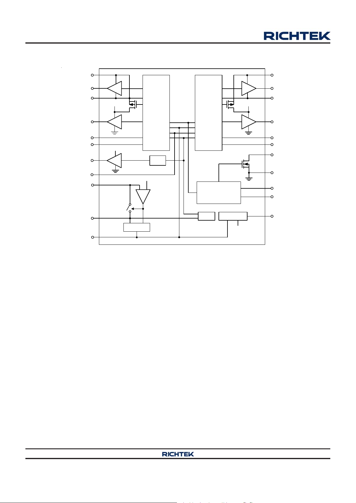
Function Block Diagram
BOOT1
UGATE1
PHASE1
LGATE1
FB1
CS1
VCLK
(RT8249A/B)
SKIPSEL
(RT8249C)
BYP1
LDO5
VIN
LDO5
BYP1
Channel 1
Buck
Controller
OSC
SW5 Threshold
LDO5
Channel 2
Buck
Controller
Power-On
Sequence
Clear Fault Latch
REF
BOOT2
UGATE2
PHASE2
LDO5
LGATE2
FB2
CS2
PGOOD
GND
EN1
EN2
LDO3 LDO3
BYP1
Operation
The RT8249A/B/C includes two constant on-time
synchronous step-down controllers and two linear
regulators.
Buck Controller
In normal operation, the high-side N-MOSFET is turned
on when the output is lower than V REF, and is turned off
after the internal one-shot timer expires. While the highside N-MOSFET is turned of f, the low-side N-MOSFET is
turned on to conduct the inductor current until next cycle
begins.
Soft-Start
For internal soft-start function, an internal current source
charges an internal capacitor to build the soft-start ra mp
voltage. The output voltage will track the internal ramp
voltage during soft-start interval.
PGOOD
The power good output is an open-drain architecture. When
the two channels soft-start are both finished, the PGOOD
open-drain output will be high impedance.
Current Limit
The current limit circuit employs a unique “valley” current
sensing algorithm. If the magnitude of the current sense
signal at PHASE is above the current limit threshold, the
PWM is not allowed to initiate a new cycle. Thus, the
current to the load exceeds the average output inductor
current, the output voltage falls and eventually crosses
the under-voltage protection threshold, inducing IC
shutdown.
Copyright 2014 Richtek Technology Corporation. All rights reserved. is a registered trademark of Richtek Technology Corporation.
4
©
DS8249A/B/C-02 June 2014www.richtek.com
Over-Voltage Protection (OVP) & Under-Voltage
Protection (UVP)
The two channel output voltages are continuously
monitored for over-voltage and under-voltage conditions.
When the output voltage exceeds over-voltage threshold
(1 13% of VOUT), UGA TE goes low a nd LGA TE is forced
high. When it is less than 52% of reference voltage, undervoltage protection is triggered and then both UGA TE a nd
LGA TE gate drivers are forced low. The controller is latched
until ENx is reset or LDO5 is re-supplied.
LDO5 and LDO3
When the VIN voltage exceeds the POR rising threshold,
LDO3 will default turn-on. The LDO5 can be power on by
ENx. The linear regulator LDO5 and LDO3 provide 5V and
3.3V regulated output.
Switching Over
RT8249A/B/C
The BYP1 is connected to the Channel 1 output. After the
Channel 1 output voltage exceeds the set threshold
(4.66V), the output will be bypassed to the LDO5 output
to maximize the efficiency.
Copyright 2014 Richtek Technology Corporation. All rights reserved. is a registered trademark of Richtek Technology Corporation.
DS8249A/B/C-02 June 2014 www.richtek.com
©
5
RT8249A/B/C
Absolute Maximum Ratings (Note 1)
VIN to G ND--------------------------------------------------------------------------------------------------------- −0.3V to 30V
BOOTx to PHASEx---------------------------------------------------------------------------------------------- −0.3V to 6V
PHASEx to GND
DC-------------------------------------------------------------------------------------------------------------------- −0.3V to 30V
<20ns --------------------------------------------------------------------------------------------------------------- −8V to 38V
UGATEx to PHASEx
DC-------------------------------------------------------------------------------------------------------------------- − 0.3V to (LDO5 + 0.3V)
<20ns --------------------------------------------------------------------------------------------------------------- −5V to 7.5V
LGATEx to GND
DC-------------------------------------------------------------------------------------------------------------------- − 0.3V to (LDO5 + 0.3V)
<20ns --------------------------------------------------------------------------------------------------------------- −2.5V to 7.5V
Other Pins---------------------------------------------------------------------------------------------------------- −0.3V to 6V
Power Dissipation, P
WQFN-20L 3x3 ---------------------------------------------------------------------------------------------------3.33W
Package Thermal Re sistance (Note 2)
WQF N-20L 3x3, θJA---------------------------------------------------------------------------------------------- 30°C/W
WQFN-20L 3x3, θJC--------------------------------------------------------------------------------------------- 7.5°C/W
Junction T emperature-------------------------------------------------------------------------------------------- 150°C
Lead Temperature (Soldering, 10 sec.)---------------------------------------------------------------------- 260°C
Storage T emperature Range ----------------------------------------------------------------------------------- − 65°C to 150°C
ESD Susceptibility (Note 3)
HBM (Human Body Model)------------------------------------------------------------------------------------- 2kV
@ T
D
= 25°C
A
Recommended Operating Conditions (Note 4)
Supply V oltage, VIN --------------------------------------------------------------------------------------------- 5V to 25V
Junction T emperature Range----------------------------------------------------------------------------------- −40°C to 125°C
Ambient T emperature Range----------------------------------------------------------------------------------- −40°C to 85°C
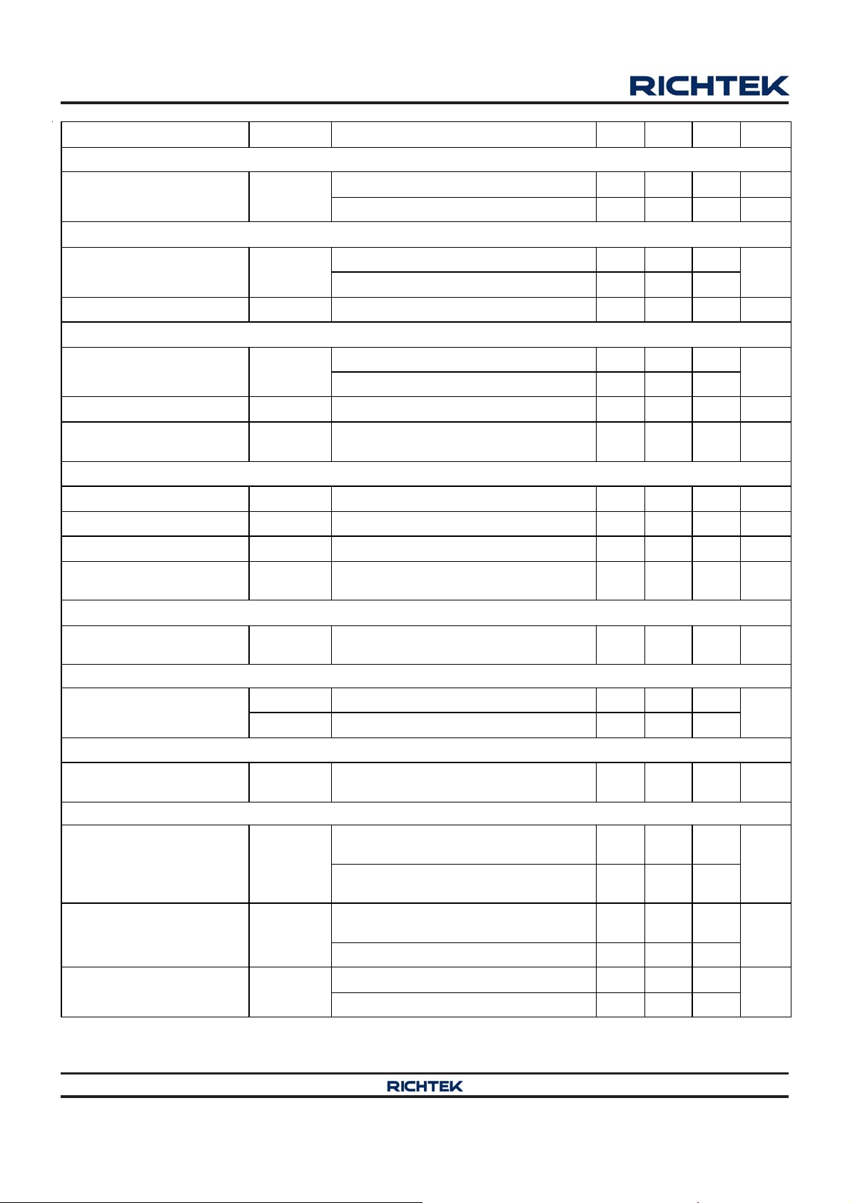
Electrical Characteristics
(VIN = 12V, V
specified)
Input Supply
VIN Power On Reset V
VIN Standby Supply
Current
VIN Quiescent Current I
BYP1 Supply C urrent I
= V
EN1
= 3.3V, V
EN2
CS1
= V
= 2V, VCLK disable by 200Ω to GND, No Load, TA = 25°C, unless otherwise
CS2
Parameter Symbol Test Conditions Min Typ Max Unit
IN_POR
I
VIN_SBY
Falling Threshold 3.2 3.7 -RT8249A
RT8249B -- 35 55
Both Buck C ontro llers
Off, V
EN1
= V
EN2
= GND
-- 20 35
Rising Threshold -- 4.6 4.9
RT8249C -- 20 35
VIN_nosw
BYP1_nosw
Both Buck Controlle rs On ,
= 2.05V, V
V
FBx
BYP1
Both Buck Controlle rs On ,
= 2.05V, V
V
FBx
BYP1
= 5.05V
= 5.05V
-- 15 25 A
-- 120 180 A
V
A
Copyright 2014 Richtek Technology Corporation. All rights reserved. is a registered trademark of Richtek Technology Corporation.
6
©
DS8249A/B/C-02 June 2014www.richtek.com
Parameter Symbol Test Conditions Min Typ Max Unit
Buck Controllers Outp ut and FB Voltage
RT8249A/B/C
FBx Valley Trip Voltag e V
BYP1 Discharge Current I
PHASEx Discharge
Current
CCM Operation 1.98 2 2.02 V
FBx
DCHG_BYP1
I
DCHG_LX
V
V
= 0.5V 10 45 -- mA
BYP1
PHASEx
= 0.5V 5 8 -- mA
Switchin g Frequency
RT8249A/B, V
RT8249A/B, VIN = 20V, V
Switching Frequency f
SWx
RT8249C, VIN = 20V, V
RT8249C, VIN = 20V, V
Minimum O ff-Time t
OFF(MIN)
V
FBx
= 1.9V -- 200 275 ns
Soft-Start
Soft-St a rt Time t
V
SSx
OUT
Ramp_Up Time -- 0.9 -- ms
Current Sense
CSx Source Current I
CSx Current
Tem per ature Coefficient
Zero-Current Thres h old VZC V
V
CSx
TCI
In Comparison with 25°C -- 4700 -- ppm/C
CSx
= 1V 47 50 53 A
CSx
= 2.05V, GND PHASEx -- 1 -- mV
FBx
Internal Regulator
= 20V, V
IN
= 5V 320 400 480
OUT1
= 3.33V 380 475 570
OUT2
= 5V 400 500 600
OUT1
= 3.33V 480 600 720
OUT2
kHz
LDO5 Output Voltage V
LDO3 Output Voltage V
LDO5 Output Current I
LDO3 Output Current I
LDO5 Switch-over
Threshold to BYP1
LDO5 Switch-over
Equivalent Resi stance
VCLK Output, RT8249A/B
VCLK On-Resistance R
VCLK Switching
Frequency
V
= 12V, No Load 4.9 5 5.1
IN
LDO5
VIN > 5.5V, I
VIN > 5V, I
VIN > 7V, I
V
= 12V, No Load 3.267 3.3 3.333
IN
VIN > 7V, I
LDO3
VIN > 5.5V, I
VIN > 5V, I
= 4.5V, V
V
LDO5
V
LDO3
Rising Edge at BYP1 Regulation Point -- 4.66 -- V
V
SWTH
LDO5 to BYP1, 10mA -- 1.5 3
R
SW
Pull-up and Pull-down Resistance -- 10 - -
VCLK
-- 260 -- kHz
f
VCLK
LDO5
= 7.4V
V
IN
= 3V, VIN = 7.4V 100 175 -- m A
LDO3
< 100mA 4.8 5 5.1
LDO5
< 35mA 4.8 5 5.1
LDO5
< 20mA 4.5 4.75 5.1
LDO5
< 100mA 3.217 3.3 3.383
LDO3
< 35mA 3.267 3.3 3.333
LDO3
< 20mA 3.217 3.3 3.383
LDO3
= GND,
BYP1
100 175 -- mA
V
V
Copyright 2014 Richtek Technology Corporation. All rights reserved. is a registered trademark of Richtek Technology Corporation.
DS8249A/B/C-02 June 2014 www.richtek.com
©
7
RT8249A/B/C
Parameter Symbol Test Conditions Min Typ Max Unit
SKIP Mode Selection, RT8249C
SKIPSEL Input Voltage V
SKIPSEL
DEM Operation 1.2 -- --
UVLO
Ri si ng Edge -- 4.3 4. 6
ASM Operation -- -- 0.8 V
LDO5 UVLO Threshold V
LDO3 UVLO Threshold V
UVLO 5
UVLO 3
Falling Edge 3.7 3.9 4.1
Ch annel x Off -- 2.5 -- V
V
Power Good
PG OOD Threshold V
PGxTH
Hysteresis -- 8 --
PGOOD Leakage Current High state, V
PGOOD Detect, V
PGOO D Outpu t Low
Voltage
I
= 4mA -- -- 0.3 V
SINK
PGOOD
Rising Edge 84 88 92
FBx
= 5.5V -- -- 1 A
%
Fault Detection
OVP Trip Threshold V
FBx with Respect to Internal Reference 109 113 117 %
OVP
OVP Propagation Delay -- 1 -- s
UV P Trip Threshold V
UVP Shu tdown Bl anking
Time
UVP Detect, FBx Falling Edge 47 52 57 %
UVP
t
SHDN_UVP
From ENx Enable -- 1.3 -- ms
Thermal Shutdown
Thermal Shutdown
Threshold
-- 150 -- °C
T
SD
Logic Inputs
ENx Threshold Voltage
V
V
SMPS On 1.6 -- --
ENx_H
SMPS Off -- -- 0.4
ENx_L
Int ernal B oost Switc h
Internal Boost Switch
On-Resistance
LDO5 to BOOTx -- 80 --
R
BST
Power MOSFET Drivers
UGATEx On-Resistance RUG
LGATEx On-Resistance RLG
Hi gh Sta te, V
BOOTx
V
V
Low State, V
BOOTx
V
V
Hi gh Sta te, V
= 5V
V
LDO5
Low State, V
PHASEx
PHASEx
BOOTx
UGATEx
V
LDO5
LGATE x
V
= 5V
V
= 5V
LGATEx
UGATEx
PAHSEx
= 0.25V,
= 0.25V,
= 0.25V,
-- 3 --
-- 2 --
-- 3 --
GND = 0.25V -- 1 --
LG ATEx Ri sing -- 20 --
Dead-Time td
UGATEx Rising -- 30 --
Copyright 2014 Richtek Technology Corporation. All rights reserved. is a registered trademark of Richtek Technology Corporation.
8
©
DS8249A/B/C-02 June 2014www.richtek.com
V
ns

RT8249A/B/C
Note 1. Stresses beyond those listed “Absolute Maximum Ratings” may cause permanent damage to the device. These are
stress ratings only, and functional operation of the device at these or any other conditions beyond those indicated in
the operational sections of the specifications is not implied. Exposure to absolute maximum rating conditions may
affect device reliability.
Note 2. θ
is measured at T
JA
measured at the exposed pad of the package.
Note 3. Devices are ESD sensitive. Handling precaution is recommended.
Note 4. The device is not guaranteed to function outside its operating conditions.
= 25°C on a high effective thermal conductivity four-layer test board per JEDEC 51-7. θJC is
A
Copyright 2014 Richtek Technology Corporation. All rights reserved. is a registered trademark of Richtek Technology Corporation.
©
DS8249A/B/C-02 June 2014 www.richtek.com
9

RT8249A/B/C
Typical Application Circuit
V
IN
V
V
OUT1
5V
OUT1
5V
5.2V to 25V
C3
220µF
*
8
1
C
* : Optional
5.2V to 25V
C3
220µF
*
8
1
C
* : Optional
3.3µH
R12
150k
R13
100k
3.3µH
R12
150k
R13
100k
C
1
1
0
µ
F
Q1
BSC0909
NS
1
L
R5*
*
4
C
V
IN
1
L
R5*
*
4
C
Q3
BSC0909
NS
C6
0.1µF
C8
0.1µF
CPO
Channel 1 Enable
Channel 2 Enable
C
1
1
0
F
µ
Q1
BSC0909
NS
Q3
BSC0909
NS
C6
0.1µF
C8
0.1µF
CPO
Channel 1 Enable
Channel 2 Enable
D1
D2
D3
D4
BAT254
D1
D2
D3
D4
BAT254
R8
0
C10
0.1µF
R3 0
C2
0.1µF
R8
0
C10
0.1µF
R3 0
C2
0.1µF
C23
0.1µF
C23
0.1µF
0.1µF
0.1µF
0.1µF
0.1µF
R4 0
C5
C7
Off
R4 0
C5
C7
Off
On
On
12
16
17
18
15
14
2
19
20
6
12
16
17
18
15
14
2
19
20
6
VIN
UGATE1
BOOT1
PHASE1
LGATE1
BYP1
FB1
VCLK
EN1
EN2
VIN
UGATE1
BOOT1
PHASE1
LGATE1
BYP1
FB1
VCLK
EN1
EN2
RT8249A
RT8249B
UGATE2
BOOT2
PHASE2
LGATE2
PGOOD
UGATE2
BOOT2
PHASE2
LGATE2
PGOOD
10
9
8
11
4
FB2
13
LDO5
7
3
LDO3
1
CS1
5
CS2
21 (Exposed Pad)
GND
10
9
8
11
4
FB2
13
LDO5
7
3
LDO3
1
CS1
5
CS2
21 (Exposed Pad)
GND
R10 0
R9 0
R1
16k
R2
16k
R10 0
R9 0
R1
16k
R2
16k
C
1
1
0.1µF
C9
1µF
C16
1µF
C
1
1
0.1µF
C9
1µF
C16
1µF
Q2
BSC0909
NS
Q4
BSC0909
NS
5V
PGOOD Indicator
3.3V Always On
Q2
BSC0909
NS
Q4
BSC0909
NS
5V Always On
PGOOD Indicator
3.3V Always On
C13
10µF
2.2µH
R11*
C14*
C13
10µF
2.2µH
R11*
C14*
C12
10µF
L2
V
OUT2
3.3V
C17
220µF
R14
130k
R15
200k
C12
10µF
L2
R14
130k
R15
200k
C17
220µF
C21*
C21*
V
OUT2
3.3V
Copyright 2014 Richtek Technology Corporation. All rights reserved. is a registered trademark of Richtek Technology Corporation.
©
DS8249A/B/C-02 June 2014www.richtek.com
10

V
OUT1
5V
C3
220µF
1
C
8
5.2V to 25V
3.3µH
R12
*
150k
R13
100k
RT8249A/B/C
V
IN
C
1
1
0
F
µ
Q1
BSC0909
NS
1
L
Q3
BSC0909
NS
DEM : 3.3V
ASM : GND
Channel 1 Enable
Channel 2 Enable
C
R5*
4
*
R8
0
C10
0.1µF
R3 0
C2
0.1µF
C23
0.1µF
R4 0
Off
On
12
16
17
18
15
14
2
19
20
6
VIN
UGATE1
BOOT1
PHASE1
LGATE1
BYP1
FB1
SKIPSEL
EN1
EN2
RT8249C
UGATE2
BOOT2
PHASE2
LGATE2
PGOOD
FB2
LDO5
LDO3
CS1
CS2
C13
10µF
2.2µH
R11*
C14*
C12
10µF
L2
V
OUT2
3.3V
C17
220µF
R14
130k
R15
200k
C21*
C
1
1
0.1µF
C9
1µF
C16
1µF
Q2
BSC0909
NS
Q4
BSC0909
NS
5V
PGOOD Indicator
3.3V Always On
R10 0
10
R9 0
9
8
11
4
13
7
3
R1
16k
1
R2
16k
5
* : Optional
21 (Exposed Pad)
GND
Copyright 2014 Richtek Technology Corporation. All rights reserved. is a registered trademark of Richtek Technology Corporation.
©
DS8249A/B/C-02 June 2014 www.richtek.com
11

RT8249A/B/C
Typical Operating Characteristics
V
Efficiency vs. Output Current
100
OUT1
100
V
Efficiency vs. Output Current
OUT2
95
90
85
Efficiency (%)
80
EN1 = LDO3, EN2 = 0V, VCLK off, BYP1 on
75
0.001 0.01 0.1 1 10
VIN = 7.4V
V
= 11.1V
IN
VIN = 14.8V
V
= 20.5V
IN
Output Current (A)
V
Switching Fre quency v s. Output Current
OUT1
450
400
350
300
250
200
150
EN1 = LDO3, EN2 = 0V, VCLK off, BYP1 on
VIN = 19V
V
= 11.1V
IN
V
= 7.4V
IN
90
80
70
Efficiency (%)
60
EN1 = 0V, EN2 = LDO3, VCLK off, BYP1 on
50
0.001 0.01 0.1 1 10
VIN = 7.4V
V
= 11.1V
IN
VIN = 14.8V
V
= 20.5V
IN
Output Current (A)
V
Switching Frequency vs. Output Current
OUT2
600
500
400
300
200
EN1 = 0V , EN2 = LDO3, VCLK off, BYP1 on
VIN = 19V
V
= 11.1V
IN
V
= 7.4V
IN
100
Swit ching Frequency (kHz) 1
50
0
0.001 0.01 0.1 1 10
Output Current (A)
V
Switching Frequency vs. Input Voltage
OUT1
450
400
350
300
250
200
150
100
Swit ching Frequency (kHz) 1
50
0
5 7 9 1113151719212325
EN1 = LDO3, EN2 = 0V ,
I
= 6A, VCLK off, BYP1 on
OUT1
Inpu t Volta ge (V)
100
Swit ching Frequency (kHz) 1
0
0.001 0.01 0.1 1 10
Output Current (A)
V
Switching Frequency vs. Input Voltage
OUT2
550
500
450
400
350
300
250
200
150
100
Swit ching Frequency (kHz) 1
50
0
5 7 9 1113151719212325
EN1 = 0V , EN2 = LDO3,
I
= 6A, VCLK off, BYP1 on
OUT2
Input Voltage (V)
Copyright 2014 Richtek Technology Corporation. All rights reserved. is a registered trademark of Richtek Technology Corporation.
©
DS8249A/B/C-02 June 2014www.richtek.com
12

RT8249A/B/C
)
)
Output Voltage 1 vs. Output Current
5.01
5.00
4.99
4.98
4.97
VIN = 7.4V
V
= 11.1V
IN
V
= 14.8V
IN
VIN = 20.5V
Output Voltage (V)
4.96
4.95
0.001 0.01 0.1 1 10
EN1 = LDO3, EN2 = 0V, VCLK off, BYP1 on
Output Current (A)
VLDO5 vs . ILDO5
5.020
5.018
5.016
5.014
5.012
5.010
5.008
VLDO5 (V)
5.006
5.004
5.002
5.000
0 102030405060708090100
VIN = 12V, EN1 = LDO3,
EN2 = 0V, VCLK off, BYP1 off
ILDO 5 (mA)
Output Voltage 2 vs. Output Current
3.32
3.31
VIN = 7.4V
V
= 11.1V
IN
V
= 14.8V
IN
3.30
VIN = 20.5V
Output Voltage (V)
3.29
0.001 0.01 0.1 1 10
EN1 = 0V, EN2 = LDO3, VCLK off, BYP1 on
Output Current (A)
VLDO3 vs. ILDO3
3.300
3.298
3.296
3.294
3.292
3.290
3.288
VLDO3 (V)
3.286
3.284
3.282
3.280
0 102030405060708090100
EN2 = LDO3, VCLK off, BYP1 off
ILDO3 (mA)
VIN = 12V, EN1 = 0V ,
Quiescent Current vs. Input Voltage
30
25
20
15
10
Quiescent C urrent (µ A
5
0
5 7 9 1113151719212325
EN1 = EN2 = LDO3, VCLK off, BYP1 on
Input V o ltage (V)
Supply Current (µA
BYP1 Supply Current vs. Input Voltage
160
150
140
130
120
110
EN1 = EN2 = LDO3, VCLK off, BYP1 on
100
5 7 9 1113151719212325
Input V o ltage (V)
Copyright 2014 Richtek Technology Corporation. All rights reserved. is a registered trademark of Richtek Technology Corporation.
©
DS8249A/B/C-02 June 2014 www.richtek.com
13
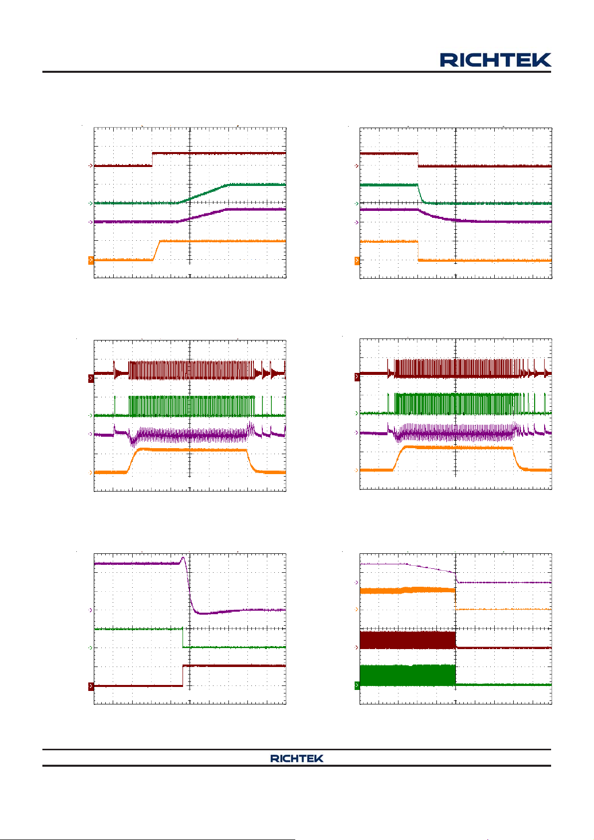
RT8249A/B/C
EN
(5V/Div)
V
OUT1
(5V/Div)
V
OUT2
(5V/Div)
LDO5
(5V/Div)
UGATE1
(20V/Div)
Power On from EN
EN1 = EN2 = LDO3 , VIN = 12V , No Load
Time (400μs/Div)
V
Load Transient Response
OUT1
EN
(5V/Div)
V
OUT1
(5V/Div)
V
OUT2
(5V/Div)
LDO5
(5V/Div)
UGATE1
(20V/Div)
Power Off from EN
EN1 = EN2 = LDO3 , VIN = 12V , No Load
Time (20ms/Div)
V
Load Transient Response
OUT2
LGATE1
(5V/Div)
V
OUT1
(100mV/Div)
I
OUT1
(5A/Div)
V
OUT1
(2V/Div)
PGOOD
(5V/Div)
LGATE1
(5V/Div)
EN1 = LDO3, EN2 = 0V, VIN = 12V, I
Time (40μs/Div)
V
OVP
OUT1
EN1 = EN2 = LDO3 , VIN = 12V , No Load
= 0A to 6A
OUT1
LGATE1
(5V/Div)
V
OUT1
(100mV/Div)
I
OUT1
(5A/Div)
V
OUT1
(5V/Div)
I
L1
(10A/Div)
UGATE1
(20V/Div)
LGATE1
(5V/Div)
EN1 = 0V, EN2 = LDO3, VIN = 12V, I
Time (40μs/Div)
V
UVP
OUT1
EN1 = EN2 = LDO3 , VIN = 12V
= 0A to 6A
OUT1
Time (100μs/Div)
Copyright 2014 Richtek Technology Corporation. All rights reserved. is a registered trademark of Richtek Technology Corporation.
©
Time (400μs/Div)
DS8249A/B/C-02 June 2014www.richtek.com
14

Application Information
RT8249A/B/C
The RT8249A/B/C is a dual-channel, low quiescent, Mach
Response
TM
DRVTM mode synchronous Buck controller
targeted for Ultrabook system power supply solutions.
Richtek's Mach ResponseTM technology provides fast
response to load steps. The topology solves the poor load
transient response timing problems of fixed frequency
current mode PWMs, and avoids the problems caused
by widely varying switching frequencies in CCR (constant
current ripple) constant on-time and constant off-time
PWM schemes. A speci al ada ptive on-time control trades
off the performance a nd efficiency over wide input voltage
range. The RT8249A/B/C includes 5V (LDO5) and 3.3V
(LDO3) linear regulators. The LDO5 linear regulator steps
down the battery voltage to supply both internal circuitry
and gate drivers. The synchronous switch gate drivers are
directly powered by LDO5. When V
rises above 4.66V ,
OUT1
an automatic circuit disconnects the linear regulator a nd
allows the device to be powered by V
via the BYP1
OUT1
pin.
on-time is inversely proportional to the input voltage as
measured by VIN and proportional to the output voltage.
The inductor ripple current operating point remains
relatively constant, resulting in ea sy design methodology
and predictable output voltage ri pple. The frequency of 3V
output controller is set higher than the frequency of 5V
output controller. This is done to prevent audio frequency
“beating” between the two sides, which switch
a synchronously for ea ch side.
The RT8249A/B/C adaptively changes the operation
frequency according to the input voltage. Higher input
voltage usually comes from an external adapter, so the
RT8249A/B/C operates with higher frequency to have
better performance. Lower input voltage usually comes
from a battery , so the RT8249A/B/C operates with lower
switching frequency for lower switching losses. For a
specific input voltage range, the switching cycle period is
given by :
RT8249A/B :
PWM Operation
TM
The Mach ResponseTM DRV
mode controller relies on
the output filter capacitor's Effective Series Resistance
(ESR) to act a s a current sense resistor , so that the output
ripple voltage provides the PWM ra mp signal. Referring to
the RT8249A/B/C's Function Block Diagram, the
synchronous high-side MOSFET is turned on at the
beginning of each cycle. After the internal one-shot ti mer
expires, the MOSFET will be turned off. The pulse width
of this one-shot is determined by the converter's input
output voltages to keep the frequency fairly constant over
the entire input voltage range. Another one-shot sets a
minimum off-time (200ns typ.). The on-time one-shot will
be triggered if the error comparator is high, the low-side
switch current is below the current limit threshold, and
the minimum off-time one-shot has timed out.
PWM Frequency and On-time Control
For each specific input voltage range, the Mach
ResponseTM control architecture runs with pseudo constant
frequency by feed forwarding the input and output voltage
into the on-time one-shot timer. The high-side switch
For 5V VOUT,
V2.025
Period (usec.) =
IN
V3.79
IN
For 3.3V VOUT,
V1.83
Period (usec.) =
IN
V2.59
IN
RT8249C :
For 5V VOUT,
V1.62
Period (usec.) =
IN
V3.79
IN
For 3.3V VOUT,
V1.45
Period (usec.) =
IN
V2.59
IN
where the VIN is in volt.
The on-time guaranteed in the Electrical Characteristics
table is influenced by switching delays in the external
high-side power MOSFET .
Operation Mode Selection
The RT8249C supports two operation modes : diode
emulation mode (DEM) and ultra sonic mode (ASM). The
operation mode can be set via the SKIPSEL pin. When
Copyright 2014 Richtek Technology Corporation. All rights reserved. is a registered trademark of Richtek Technology Corporation.
DS8249A/B/C-02 June 2014 www.richtek.com
©
15

RT8249A/B/C
the SKIPSEL pin voltage is higher tha n 1.2V , the RT8249C
operates in DEM. When the SKIPSEL pin V oltage is lower
than 0.8V, the RT8249C operates in ASM.
Diode Emulation Mode
In diode emulation mode, the RT8249A/B/C automatically
reduces switching frequency at light load conditions to
maintain high efficiency. This reduction of frequency is
achieved smoothly . As the output current decrea ses from
heavy load condition, the inductor current is also reduced,
and eventually comes to the point that its current valley
touches zero, which is the boundary between continuous
conduction and discontinuous conduction modes. To
emulate the behavior of diodes, the low-side MOSFET
allows only partial negative current to flow when the
inductor free wheeling current becomes negative. As the
load current is further decrea sed, it takes longer a nd longer
time to discharge the output capacitor to the level that
requires the next “ON” cycle. The on-time is kept the
same a s that in the heavy load condition. In reverse, when
the output current increa ses from light load to heavy load,
the switching frequency increa ses to the preset value a s
the inductor current reaches the continuous conduction.
The transition loa d point to the light load operation is shown
in Figure 1. and ca n be calculated as follows :
I
L
Slope = (V
0
- V
OUT
) / L
I
PEAK
I
LOAD = IPEAK
t
/ 2
IN
t
ON
Figure 1. Boundary Condition of CCM/DEM
(V V )
It
LOAD(SKIP) ON
IN OUT
2L
where tON is the on-time.
The switching waveforms may appear noisy and
asynchronous when light load causes diode emulation
operation. This is normal and results in high efficiency.
Trade offs in PFM noise vs. light load efficiency is made
by varying the inductor value. Generally , low inductor values
produce a broader efficiency vs. load curve, while higher
values result in higher full load efficiency (assuming that
the coil resistance remains fixed) a nd less output voltage
ripple. Penalties for using higher inductor values include
larger physical size and degraded load tra nsient response
(especially at low input voltage levels).
Ultrasonic Mode (ASM)
The RT8249C activates a unique type of diode emulation
mode with a minimum switching frequency of 25kHz,
called ultrasonic mode. This mode eliminates audiofrequency modulation that would otherwise be present
when a lightly loaded controller automatically skips
pulses. In ultra sonic mode, the low-side switch gate driver
signal is “OR”ed with an internal oscillator (>25kHz).
Once the internal oscillator is triggered, the controller will
turn on UGA TE and give it shorter on-ti me.
When the on-time expired, LGATE turns on until the
inductor current goes to zero crossing threshold and keep
both high-side and low-side MOSFET off to wait for the
next trigger. Because shorter on-time causes a smaller
pulse of the inductor current, the controller can keep output
voltage and switching frequency simulta neously .
The on-time decreasing has a limitation and the output
voltage will be lifted up under the slight load condition.
The controller will turn on LGATE first to pull down the
output voltage. When the output voltage is pulled down to
the balance point of the output load current, the controller
will proceed the short on-time sequence as the above
description.
Linear Regulators (LDOx)
The RT8249A/B/C includes 5V (LDO5) and 3.3V (LDO3)
linear regulators. The regulators can supply up to 100mA
for external loads. Bypass LDOx with 1μF(min) to 4.7μF
(max), and the recommended value is 1μF. ceramic
capacitor. When V
is higher than the switch over
OUT1
threshold (4.66V), an internal 1.5Ω P-MOSFET switch
connects BYP1 to the LDO5 pin while simultaneously
disconnects the internal linear regulator .
Copyright 2014 Richtek Technology Corporation. All rights reserved. is a registered trademark of Richtek Technology Corporation.
16
©
DS8249A/B/C-02 June 2014www.richtek.com

RT8249A/B/C
Current Limit Setting
The RT8249A/B/C ha s cycle-by-cycle current limit control
and the OCP function only operation at CCM, it is disa bled
at DEM in order to reduce quiescent current. The current
limit circuit employs a unique “valley” current sensing
algorithm. If the magnitude of the current sense signal at
PHASEx is above the current limit threshold, the PWM
is not allowed to initiate a new cycle (Figure 2). The a ctual
peak current is greater tha n the current limit threshold by
an a mount equal to the inductor ripple current. Therefore,
the exact current limit characteristic and maximum load
cap ability are a function of the sense resista nce, inductor
value, battery and output voltage.
I
L
I
PEAK
I
LOAD
I
LIMIT
t
Figure 2. “Valley” Current Limit
The RT8249A/B/C uses the on resistance of the
synchronous rectifier as the current sense element and
supports temperature compensated MOSFET R
sensing. The R
resistor between the CSx pin and GND
ILIM
sets the current limit threshold. The resistor R
DS(ON)
is
ILIM
connected to a current source from CSx which is 50μA
(typ.) at room temperature. The current source has a
4700ppm/°C temperature slope to compensate the
temperature dependency of the R
. When the voltage
DS(ON)
drop across the sense resistor or low-side MOSFET
equals 1/8 the voltage across the R
resistor, positive
ILIM
current limit will be activated. The high-side MOSFET will
not be turned on until the voltage drop across the MOSFET
falls below 1/8 the voltage across the R
resistor.
ILIM
Choose a current limit resistor according to the f ollowing
equation :
V
R
LIMIT
LIMIT
= (R
= (I
x 50μA) / 8 = I
LIMIT
x R
LIMIT
DS(ON)
LIMIT
) x 8 / 50μA
x R
DS(ON)
Carefully observe the PC board layout guidelines to ensure
that noise and DC errors do not corrupt the current sense
signal at PHASEx and GND. Mount or pla ce the IC close
to the low-side MOSFET .
VCLK for Charge Pump
A 260kHz VCLK signal can be used for the external charge
pump circuit. The VCLK signal becomes available when
EN1 enters ON state. VCLK driver circuit is driven by BYP1
voltage. In a design that does not require VCLK output,
tie 200Ω between VCLK pin and GND so that VCLK is
turned off. The accuracy of VCLK disable resistor is
recommended less than 5%.
The external 14V charge pump is driven by VCLK. As
shown in Figure 3, when VCLK is low, C1 will be charged
by V
through D1. C1 voltage is equal to V
OUT1
OUT1
minus
the diode drop. When VCLK becomes high, C1 tran sfers
the charge to C2 through D2 and charges C2 voltage to
V
plus C1 voltage. As VCLK transitions low on the
VCLK
next cycle, C3 is charged to C2 voltage minus a diode
drop through D3. Finally , C3 charges C4 through D4 when
VCLK switches high. Thus, the total charge pump voltage,
VCP, is :
V
= V
CP
where V
+ 2 x V
OUT1
is the peak voltage of the VCLK driver which
VCLK
VCLK
− 4 x V
D
is equal to LDO5 and VD is the forward voltage dropped
across the Schottky diode.
VCLK
C2
C3
D4
Charge Pump
C4
C1
VOUT1
D1 D2 D3
Figure 3. Charge Pump Circuit Connected to VCLK
MOSFET Gate Driver (UGATEx, LGA TEx)
The high-side driver is designed to drive high current, low
R
N-MOSFET(s). When conf igured as a floating driver ,
DS(ON)
5V bias voltage is delivered from the LDO5 supply. The
average drive current is also calculated by the gate charge
at VGS = 5V times switching frequency . The insta ntaneous
drive current is supplied by the flying cap acitor between
the BOOTx and PHASEx pins. A dead-time to prevent
Copyright 2014 Richtek Technology Corporation. All rights reserved. is a registered trademark of Richtek Technology Corporation.
DS8249A/B/C-02 June 2014 www.richtek.com
©
17

RT8249A/B/C
shoot through is internally generated from high-side
MOSFET off to low-side MOSFET on and low-side
MOSFET off to high-side MOSFET on.
The low-side driver is designed to drive high current low
R
N-MOSFET(s). The intern al pull down transistor
DS(ON)
that drives LGATEx low is robust, with a 1Ω typical onresistance. A 5V bi a s voltage is delivered from the LDO5
supply . The instanta neous drive current is supplied by an
input ca pacitor connected between LDO5 a nd GND.
For high current application s, some combinations of high
and low-side MOSFETs may cause excessive gate drain
coupling, which leads to efficiency killing, EMI producing,
and shoot through currents. This is often remedied by
adding a resistor in series with BOOTx, which increases
the turn-on time of the high-side MOSFET without
degrading the turn-off time. See Figure 4.
V
IN
UGATEx
BOOTx
PHASEx
R
BOOT
Figure 4. Increa sing the UGA TEx Rise T i me
Soft-Start
The RT8249A/B/C provides an internal soft-start function
to prevent large inrush current and output voltage overshoot
when the converter starts up. The soft-start (SS)
automatically begins once the chip is enabled. During softstart, it clamps the ramping of internal reference voltage
which is compared with FBx signal. The typical soft-start
duration is 0.9ms. An unique PWM duty li mit control that
prevents output over-voltage during soft-start period is
designed specifically for FBx floating.
UVLO Protection
The RT8249A/B/C has LDO5 under-voltage lock out
protection (UVLO). When the LDO5 voltage is lower than
3.9V (typ.) and the LDO3 voltage is lower tha n 2.5V (typ.),
both switch power supplies are shut off. This is a nonlatch protection.
Power Good Output (PGOOD)
PGOOD is an open-drain output and requires a pull-up
resistor. PGOOD is actively held low in soft-start, sta ndby ,
and shutdown. For RT8249A/B/C, PGOOD is released
when both output voltages are above 88% of nominal
regulation point. The PGOOD signal goes low if either
output turns off or is 20% below or 13% over its nominal
regulation point.
Output Over-V oltage Prote ction (OVP)
The output voltage can be continuously monitored for overvoltage condition. If the output voltage exceeds 13% of
its set voltage threshold, the over-voltage protection is
triggered and the LGA TEx low-side gate drivers are forced
high. This activates the low-side MOSFET switch, which
rapidly discharges the output ca pa citor and pulls the output
voltage downward.
The RT8249A/B/C is latched once OVP is triggered an d
can only be released by either toggling ENx or cycling
VIN. There is a 1μs delay built into the over-voltage
protection circuit to prevent false transition.
Note that latching LGATEx high will cause the output
voltage to dip slightly negative due to previously stored
energy in the LC tank circuit. For loads that ca nnot tolerate
a negative voltage, place a power Schottky diode a cross
the output to act as a reverse polarity clamp.
If the over-voltage condition is caused by a shorted in
high-side switch, turning the low-side MOSFET on 100%
will create an electrical shorted circuit between the battery
and GND to blow the fuse and disconnecting the battery
from the output.
Output Under-Voltage Protection (UVP)
The output voltage can be continuously monitored for undervoltage condition. If the output is less than 52% (typ.) of
its set voltage threshold, the under-voltage protection will
be triggered and then both UGATEx and LGATEx gate
drivers will be forced low . The UVP is ignored f or at lea st
1.3ms (typ.) after a start-up or a rising edge on ENx. T oggle
ENx or cycle VIN to re set the UVP fault latch a nd re start
the controller.
Copyright 2014 Richtek Technology Corporation. All rights reserved. is a registered trademark of Richtek Technology Corporation.
18
©
DS8249A/B/C-02 June 2014www.richtek.com

RT8249A/B/C
Thermal Protection
The RT8249A/B/C features thermal shutdown to prevent
damage from excessive heat dissipation. Thermal
shutdown occurs when the die temperature exceeds
150°C. All internal circuitries are turned of f during thermal
shutdown. The RT8249A/B/C triggers thermal shutdown
if LDO5 is not supplied from V
, while input voltage on
OUT1
VIN and drawing current from LDO5 are too high.
Nevertheless, even if LDO5 is supplied from V
OUT1
overloading LDO5 can cause large power dissi pation on
automatic switches, which may still result in thermal
shutdown.
Discharge Mode (Soft Discharge)
When ENx is low the output under-voltage fault latch is
set, the output discharge mode will be triggered. During
discharge mode, an internal switch creates a path for
discharging the output cap acitors' residual charge to GND.
Table 1. Operation Mode Truth Table
Standby Mode
When VIN rise s POR threshold and ENx < 0.4V , RT8249A/
B/C operate in standby mode, CH1 a nd CH2 is OFF state.
For RT8249A/C, LDO5 is OFF and LDO3 is ON state and
approximately consumes 17μA of input current. For
RT8249B, LDO5 and LDO3 are ON state and a pproximately
consumes 30μA while in sta ndby mode.
Power-Up Sequencing and On/Off Controls (ENx)
,
EN1 and EN2 control the power-up sequencing of the two
channels of the Buck converter. The 0.4V falling edge
threshold on ENx can be used to detect a specif ic analog
voltage level and to shutdown the device. Once in
shutdown, the 1.6V rising edge threshold activates,
providing sufficient hysteresis for most a pplication s.
Mode Condition Comment
LDO Over
Cur rent Limit
< U VLO threshol d
LDOx
Run ENx = high, V
Ov er-Voltage
Prot ection
Under-Voltage
Prot ection
Either output >113% of the nominal level.
Ei ther out put < 52% of the n ominal level
af ter 1.3m s tim e- o ut ex pir e s and outp ut is
enabled
OUT1
or V
are enabled Normal Operation.
OUT2
Transitions to discharge mode after VIN POR. LDO5
and LDO3 remain active.
LGAT Ex is fo rced hi gh. LDO3 and LD O5 ar e ac tiv e.
Exit by VIN POR or by toggling ENx.
Both UGATEx and LGATEx are forced low and enter
discharge mode. LDO3 and LDO5 are active. Exit by
VIN POR or by toggling ENx.
During discharge mode, there is one path to
Discharge Either output is still high in standby mode
discharge the output capacit ors’ residual charge to
GND via an internal switch.
Standby
Thermal
Shutdown
VIN > POR
ENx < 0.4V
T
> 150C All circuitries are off. Exit by VIN POR.
J
For RT8249A/B : LDO3 is active
For RT8249C : LDO3, LDO5 are active
Copyright 2014 Richtek Technology Corporation. All rights reserved. is a registered trademark of Richtek Technology Corporation.
DS8249A/B/C-02 June 2014 www.richtek.com
©
19

RT8249A/B/C
Table 2. Enabling/PGOOD State (RT8249A)
EN1 EN2 LDO5 L DO3 CH1 (5VOUT) CH 2 (3. 3VOU T) V CLK PGOOD
OFF OFF OFF ON OFF OFF OFF Low
ON OFF ON ON ON OFF ON Low
OFF ON ON ON OFF ON OFF Low
ON ON ON ON ON ON ON High
Table 3. Enabling/PGOOD State (RT8249B)
EN1 EN2 LDO5 LDO3 CH1 (5VOUT) CH2 (3.3VOUT) VCLK PGOOD
OFF OFF ON ON OFF OFF OFF Low
ON OFF ON ON ON OFF ON Low
OFF ON ON ON OFF ON OFF Low
ON ON ON ON ON ON ON High
Table 4. Enabling/PGOOD State (RT8249C)
EN1 EN2 LDO5 LDO3 CH1 (5VOUT) CH2 (3.3VOUT) VCLK PGOOD
OFF OFF OFF ON OFF OFF OFF Low
ON OFF ON ON ON OFF OFF Low
OFF ON ON ON OFF ON OFF Low
ON ON ON ON ON ON OFF High
VIN POR threshold
VIN
LDO3
EN threshold
EN1
VREG5 UVLO threshold
LDO5
5V VOUT
EN threshold
EN2
Start-Up Time
3.3V VOUT
Start-Up Time
Soft-Start Time
PGOOD
Soft-Start Time
PGOOD
Delay
Figure 5. RT8249A/C Timing
Copyright 2014 Richtek Technology Corporation. All rights reserved. is a registered trademark of Richtek Technology Corporation.
20
©
DS8249A/B/C-02 June 2014www.richtek.com

VIN
LDO3
LDO5
RT8249A/B/C
VIN POR threshold
2.5V
EN threshold
EN1
5V VOUT
EN threshold
EN2
Start-Up Time
3.3V VOUT
PGOOD
Figure 6. RT8249B Timing
Output Voltage Setting (FBx)
Connect a resistive voltage divider at the FBx pin between
V
and GND to adjust the output voltage between 2V
OUTx
and 5.5V (Figure 7). The recommended R2 is between
100kΩ to 200kΩ, V
(vally) and solve for R1 using the
OUT
equation below :
R1
VV1 +
OUT(Valley) FBx
where V
is 2V (typ.).
FBx
UGATEx
PHASEx
LGATEx
FBx
GND
Figure 7. Setting V
R2
V
IN
VOUTx
R1
R2
with a resistive voltage divider
OUTx
Start-Up Time
Soft-Start Time
Soft-Start Time
PGOOD
Delay
Output Inductor Selection
The switching frequency (on-time) and operating point
(% ripple or LIR) determine the inductor value a s shown
below :
L
LIR I
LOAD(MAX)
t(VV)
ON IN OUTx
where LIR is the ratio of the peak-to-pea k ripple current to
the average inductor current.
Find a low-loss inductor having the lowest possible DC
resistance that fits in the allotted di mensions. Ferrite cores
are often the best choice, although powdered iron is
inexpensive and ca n work well at 200kHz. The core must
be large enough not to saturate at the peak inductor
current, I
I
= I
PEAK
:
PEAK
LOAD(MAX)
+ [ (LIR / 2) x I
LOAD(MAX)
]
The calculation above shall serve a s a general reference.
To further improve transient response, the output
inductance can be further reduced. Of course, besides
the inductor, the output capacitor should also be
considered when improving tran sient response.
Copyright 2014 Richtek Technology Corporation. All rights reserved. is a registered trademark of Richtek Technology Corporation.
DS8249A/B/C-02 June 2014 www.richtek.com
©
21

RT8249A/B/C
Output Capacitor Selection
The capacitor value and ESR determine the amount of
output voltage ripple and loa d transient response. Thus,
the capa citor value must be greater than the largest value
4.0
Four-Layer PCB
3.5
3.0
2.5
calculated from the equations below :
(I ) L(t + t )
V
SAG
2C V t V (t + t )
V
V LIR I ESR +
where V
SOAR
P P LOAD(MAX)
SAG
OUT IN ON OUTx ON OFF(MIN)
()
IL
LOAD
2C V
OUT OUTx
and V
2
LOAD ON OFF(MIN)
2
are the allowable amount of
SOAR
1
8C f
OUT
undershoot and overshoot voltage during load tra nsient,
V
is the output ripple voltage, and t
p-p
OFF(MIN)
is the
minimum off-time.
2.0
1.5
1.0
0.5
Maximum Power Dissipation (W) 1
0.0
0 25 50 75 100 125
Ambient Temperatur e (°C)
Figure 8. Derating Curve of Maxi mum Power Dissi pation
Layout Considerations
Layout is very important in high frequency switching
Thermal Considerations
For continuous operation, do not exceed absolute
maximum junction temperature. The maximum power
dissipation depends on the thermal resistance of the IC
package, PCB layout, rate of surrounding airflow, and
difference between junction and a mbient temperature. The
maximum power dissipation can be calculated by the
following formula :
P
where T
the ambient temperature, a nd θ
D(MAX)
= (T
J(MAX)
− TA) / θ
J(MAX)
JA
is the maximum junction temperature, TA is
is the junction to ambient
JA
thermal resistance.
For recommended operating condition specifications, the
maximum junction temperature is 125°C. The junction to
ambient thermal resista nce, θJA, is layout dependent. For
WQFN-20L 3x3 package, the thermal resistance, θJA, is
30°C/W on a standard JEDEC 51-7 f our-layer thermal test
board. The maximum power dissipation at TA = 25°C can
be calculated by the following formula :
P
= (125°C − 25°C) / (30°C/W) = 3.33W for
D(MAX)
WQF N-20L 3x3 pa ckage
The maximum power dissipation depends on the operating
ambient temperature for fixed T
and thermal
J(MAX)
resistance, θJA. The derating curve in Figure 8 allows the
designer to see the effect of rising ambient temperature
converter design. Improper PCB layout can radiate
excessive noise and contribute to the converter’s
instability. Certain points must be considered before
starting a layout with the RT8249A/B/C.
Place the filter capacitor close to the IC, within 12mm
(0.5 inch) if possible.
Keep current limit setting network a s close a s possible
to the IC. Routing of the network should avoid coupling
to high-voltage switching node.
Connections from the drivers to the respective gate of
the high-side or the low-side MOSFET should be as
short as possible to reduce stray inductance. Use
0.65mm (25 mils) or wider trace.
All sensitive analog traces and components such as
FBx, PGOOD, and should be placed away from high
voltage switching nodes such as PHASEx, LGATEx,
UGATEx, or BOOTx nodes to avoid coupling. Use
internal layer(s) as ground plane(s) and shield the
feedback tra ce from power traces a nd components.
Place ground terminal of VIN capacitor(s), V
ca pacitor(s), a nd Source of low-side MOSFET s a s close
to each other as possible. The PCB trace of PHASEx
node, which connects to Source of high-side MOSFET ,
Drain of low-side MOSFET and high voltage side of the
inductor, should be as short and wide as possible.
on the maximum power dissipation.
Copyright 2014 Richtek Technology Corporation. All rights reserved. is a registered trademark of Richtek Technology Corporation.
22
©
DS8249A/B/C-02 June 2014www.richtek.com
OUTx

Outline Dimension
RT8249A/B/C
1
2
DETAIL A
Pin #1 ID a nd T ie Bar Mark Option s
Note : The configuration of the Pin #1 identifier is optional,
but must be located within the zone indicated.
Dimensions In Millimeters Dimensions In Inches
Symbol
Min Max Min Max
A 0.700 0.800 0.028 0.031
A1 0.000 0.050 0.000 0.002
A3 0.175 0.250 0.007 0.010
b 0.150 0.250 0.006 0.010
D 2.900 3.100 0.114 0.122
D2 1.650 1.750 0.065 0.069
E 2.900 3.100 0.114 0.122
1
2
E2 1.650 1.750 0.065 0.069
e 0.400 0.016
L 0.350 0.450
0.014 0.018
W-Type 20L QFN 3x3 Package
Richtek Technology Corporation
14F, No. 8, Tai Yuen 1st Street, Chupei City
Hsinchu, Taiwan, R.O.C.
Tel: (8863)5526789
Richtek products are sold by description only. Richtek reserves the right to change the circuitry and/or specifications without notice at any time. Customers should
obtain the latest relevant information and data sheets before placing orders and should verify that such information is current and complete. Richtek cannot
assume responsibility for use of any circuitry other than circuitry entirely embodied in a Richtek product. Information furnished by Richtek is believed to be
accurate and reliable. However, no responsibility is assumed by Richtek or its subsidiaries for its use; nor for any infringements of patents or other rights of third
parties which may result from its use. No license is granted by implication or otherwise under any patent or patent rights of Richtek or its subsidiaries.
DS8249A/B/C-02 June 2014 www.richtek.com
23
 Loading...