


CX 890

PIONEER ELECTRONIC CORPORATION 4-1, Meguro 1-Chome, Meguro-ku, Tokyo 153-8654, Japan
PIONEER ELECTRONICS SERVICE INC. P.O.Box 1760, Long Beach, CA 90801-1760 U.S.A.
PIONEER ELECTRONIC [EUROPE] N.V. Haven 1087 Keetberglaan 1, 9120 Melsele, Belgium
PIONEER ELECTRONICS ASIACENTRE PTE.LTD. 253 Alexandra Road, #04-01, Singapore 159936
C PIONEER ELECTRONIC CORPORATION 1999
K-ZZS. FEB. 1999 Printed in Japan
ORDER NO.
CRT2376
CD MECHANISM MODULE
CX-890
CONTENTS
1. MAIN PARTS LOCATIONS........................................2
2. CIRCUIT DESCRIPTIONS ..........................................3
3. MECHANISM OPERATIONS...................................16
4. DISASSEMBLY ........................................................21
NOTE:
- This Service Manual outlines operations of the CD mechanism module used in the models listed blow.
- For repair, use this Service Manual and the Service Manual of the model used in the system.
Model Service manual CD mechanism module CD mechanism unit
CDX-PD6/UC CRT2372 CXK4701 CXB2700

2
CX-890
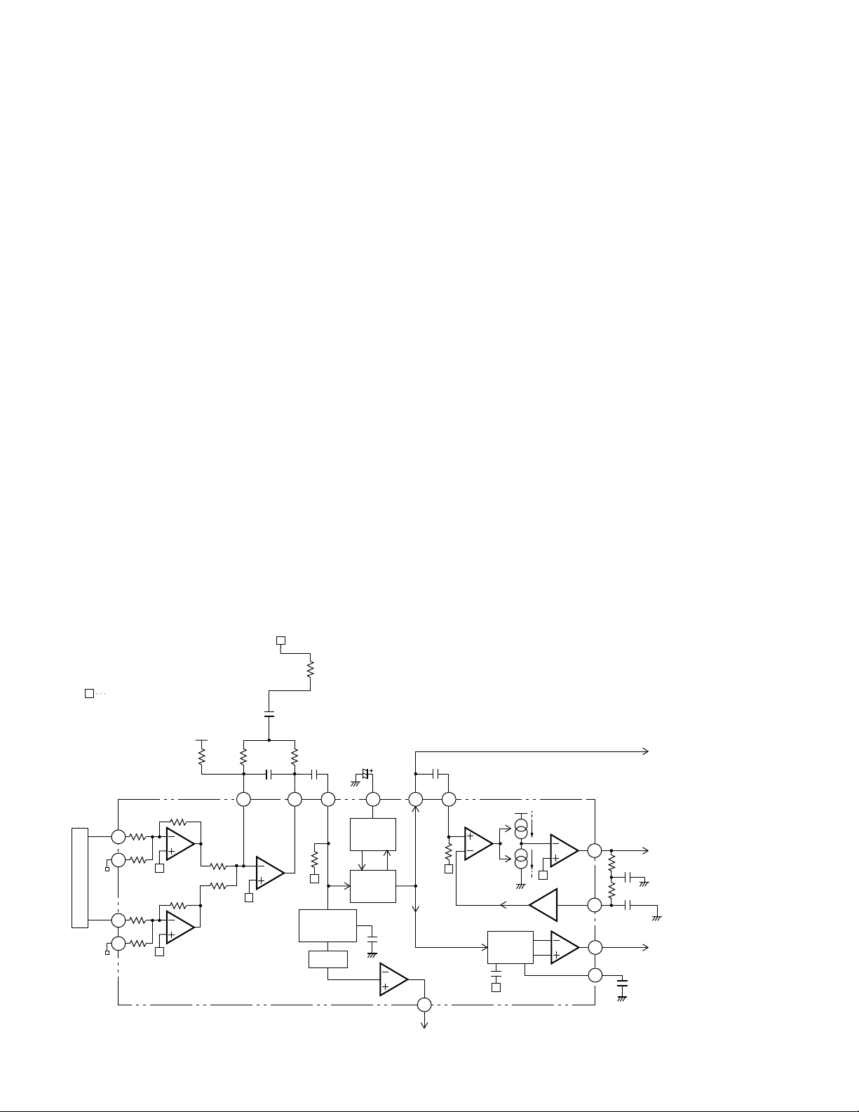
1. MAIN PARTS LOCATIONS
Frame
Stage front side
Carriage motor (M4)
ELV motor (M2)
Cam gear motor (M1)
Photo interrupter (ELV)
Loading motor (M3)
Servo unit
Disc insertion detectors
Disc insertion detectors
Clamp switch
(S887)
ELV HOME switch
(S886)
Disc ejection detectors
Detection switch
(S885)
STS unit
Spindle
motor (M5)
Insertion completion
switch
Mode switch
(S803)
Door switch
(S802)
Load switch
(S801)
Do not hold the upper frame of the disc insertion slot or
the front side of the stage in the CD mechanism module when
servicing to prevent them from being deformed.
- CD Player Service Precautions
1. For pickup unit(CXX1311) handling, please refer
to"Disassembly"(Page 21).
During replacement, handling precautions shall be
taken to prevent an electrostatic discharge(protection
by a short pin).
2. During disassembly, be sure to turn the power off
since an internal IC might be destroyed when a con-
nector is plugged or unplugged.
3
CX-890
2. CIRCUIT DESCRIPTIONS
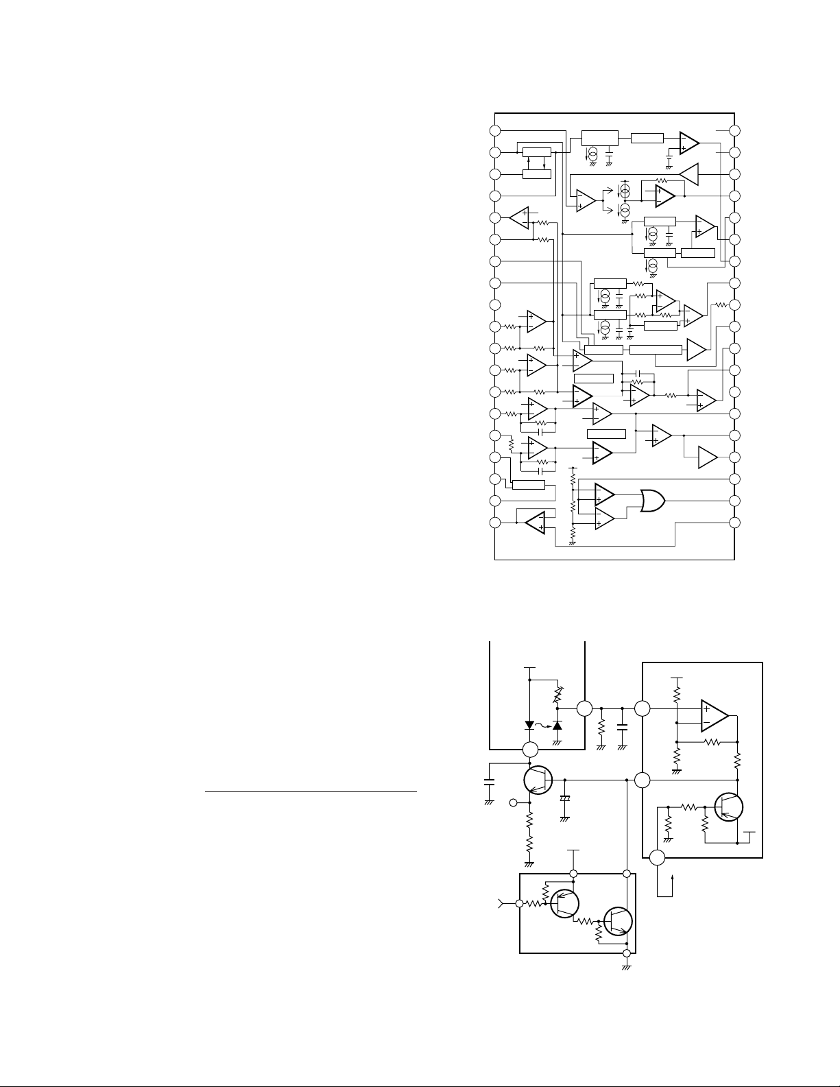
2.1 Preamplifier (UPC2572GS: IC101)
The preamplifier processes pickup output signals to
generate signals to be sent to the servo, demodulator,
and controller. The preamplifier with built-in photode-
tector converts signals from the pickup into intermedi-
ate voltage in the pickup. Then, addition is made in the
RF amplifier (IC101) to obtain RF, FE, TE, and TE zero
cross signals. The system consists of the UPC2572GS
and other components explained below. The system
uses a single power source (+5 V). Therefore, the refer-
ence voltage of IC101 and the reference voltage of the
power unit and servo circuit are REFOUT (+2.5 V). REFO
UT is obtained from REFOUT of servo LSI (IC201:
UPD63702GF) via a buffer, and is output from Pin 19 of
IC101. This REFOUT is used as reference for all mea-
surements.
Note:Do NOT short-circuit REFOUT and GND during
measurement.
1
2
3
4
5
6
7
8
9
10
11
12
13
14
15
16
17
18
19
38
37
36
35
34
33
32
31
30
29
28
27
26
25
24
23
22
21
20
X12
RF
envelope
AGC
Detection
X3
Phase detection
3T detection
Bottom
DC shift
Peak
Control
DC shift
Bottom
Peak
120kΩ
DEFECT circuit
FE
BAL
FE
BAL
Vcc
Mirror circuit
FE
BAL
APC
X2
Vcc
FE-BAL
TE-BAL
ASY
EFM-OUT
C.DEF
DEFECT
RFOK
MIRR
3T-OUT
C.FE
FE-OUT
FE-
GND
TE-
TE-OUT1
TE-OUT2
DET-IN
DET-OUT
VREF-INVREF-OUT
LDON
LD
PD
E
F
D
B
C
A
Vcc
C2.3T
C1.3T
RF-
RF-OUT
RF-IN
C AGC
AGC-OUT
EFM-IN
HPF
TE
BAL
EFM comparator
Control
Fig. 1 Block Diagram of UPC2572GS
1) Automatic Power Control (APC) circuit
Laser diode has negative temperature characteristics
with great optical output when the diode is driven with
constant current. Therefore, current must be controlled
by a monitor diode to ensure constant output. Thus
functions the APC circuit. LD current can be obtained by
measuring the voltage between LD1 and GND. The cur-
rent value is approximately 35 mA.
Vcc (5V)
Vr
LD MD
UPC2572GS
16
PD
17
LD
15
Q101
2SD1664
C124
0.1µF
C101
(100µF/6.3V)
R101
10Ω
LD1
R102
12Ω
5V
CONT
Q102 UMD2N
18
5V
5V
1kΩ
150kΩ
16kΩ
R112
2.2kΩ
C104
0.33µF
5
1kΩ
2.5V
Pickup unit
Fig. 2 APC Circuit
Voltage between LD1 and GND(mv)
LD current(mA) =
10 Ω + 12 Ω
4
CX-890
2) RF amplifier and RF AGC amplifier
Photodetector outputs (A+C) and (B+D) are added,
amplified and equalized in IC101, and output to the RFI
terminal as RF signal. (Eye pattern can be checked at
this terminal.)
Low-frequency components of voltage RFI is:
RFI = ((A + C) + (B + D)) x 3.22
where R111 is offset resistor to keep RFI signal within
the output range of the preamplifier. RFI signal is goes
under AC coupling, and is input to Pin 4 (RFIN termi-
nal).
IC101 contains an RF AGC circuit. RFO output from Pin
2 is maintained to a constant level (1.2 ±0.2 Vp-p). The
RFO signal is used in the EFM, DFCT, and MIRR circuits.
3) EFM circuit
The EFM circuit converts RF signal into digital signals of
"0" and "1". RFO signal after AC coupling is input to Pin
1, and supplied to the EFM circuit.
Asymmetry caused during manufacturing of discs can-
not be eliminated solely by AC coupling. Therefore, the
system controls the reference voltage ASY of the EFM
comparator by using the fact that probability to gener-
ate "0" and "1" is 50% in EFM signal. This reference volt-
age ASY is generated by output from the EFM com-
parator through L.P.F. EFM signal is output from Pin 35.
As signal level, amplification is 2.5 Vp-p around
REFOUT.
4) DFCT (defect) circuit
DFCT signal detects mirror defect in discs, and is output
from Pin 33. The system outputs "H" when a mirror
defect is detected.
If disc is soiled, the system determines it as lack of mir-
ror. Therefore, the system inputs the DFCT signal out-
put to the HOLD terminal of servo LSI. Focus and track-
ing servo drives change to Hold status only when DFCT
output is in "H" so that performance of the system upon
detection of defect can be improved.
5) RFOK circuit
The RFOK circuit outputs signal to show the timing of
focus closing servo, as well as the status of focus clos-
ing during playback. The signal is output from Pin 32.
The system inputs the RFOK signal output to the RFOK
terminal of servo LSI. The servo LSI issues Focus Close
command. The system outputs signal in "H" during
focus closing and playback.
CN101
13
6
DETECT
13
11
10
10kΩ
20kΩ
9.3kΩ
RFI
+5V
R111
27kΩ
Vcc
×12
ASY
12
20kΩ
(RF AGC)
AGC
RF
ENVELOPE
HPF
VDC
RFOK
20kΩ
33
36
35
34
PEAK
DEFECT
EFM
UPC2572GS
A+C
10kΩ
B+D
9.3kΩ
20kΩ
10kΩ
10kΩ
R105
6.8kΩ
C125 5pF
C105
24pF
R125
0R0
R104
8.2kΩ
RFIN
C107
4.7µF/35V
C122
0.1µF
C106
RFO
REFOUT (+2.5V)
DEFECT
BOTTOM
R107 8.2kΩ
R106 18kΩ
C111 3300pF
C110
C112 0.047µF
6 54 3 21
32
0.1µF
2200pF
HOLD
Fig. 3 RF AMP, RF AGC, EFM, DFCT, RFOK Circuit
5
CX-890
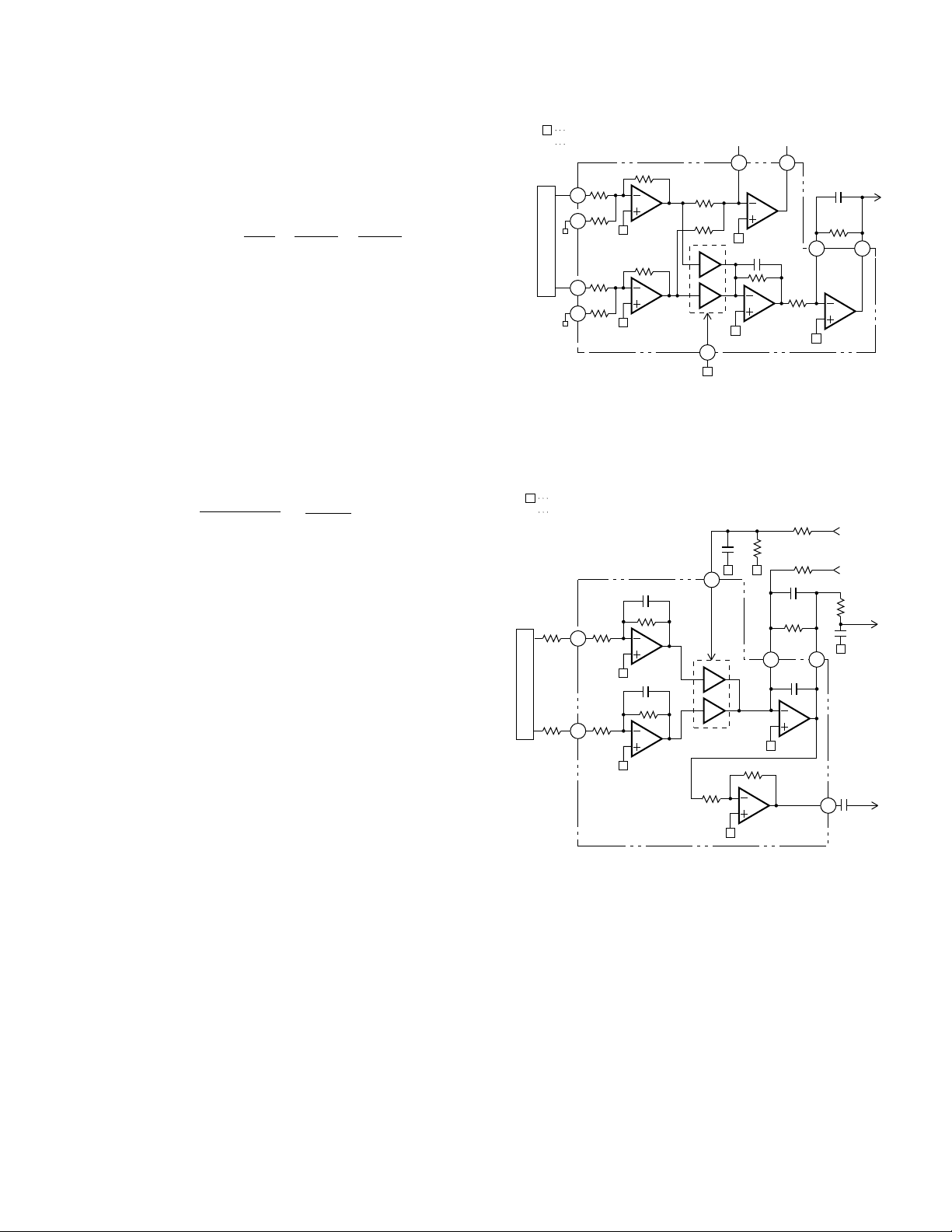
6) Focus-error amplifier
The system outputs photodetector output (A+C) and
(B+D) as FE signal (A+C)-(B+D) from Pin 28 via the dif-
ference amplifier, then via the error amplifier.
Low-frequency components of voltage FEY is:
An S curve equivalent to approximately 1.6 Vp-p is
obtained at FE output (Pin 28) by using REFO as refer-
ence. The cut-off frequency of the amplifier of the last
layer is 12.4 kHz.
7) Tracking-error amplifier
Outputs E and F from the photodetector are output as
TE signal (E-F) from Pin 24 via the difference amplifier,
then via the error amplifier.
Low-frequency components of voltage TEY is:
TE waveforms equivalent to approximately 1.5 Vp-p are
obtained at TE output (Pin 24) by using REFO as refer-
ence. The cut-off frequency of the amplifier of the last
layer is 19.5 kHz.
8) Tracking zero-cross amplifier
Tracking zero-cross signal (TEC signal) is generated by
amplifying TE waveforms (voltage at Pin 24) by a factor
of four. The signal is used for detecting the zero-cross
point of tracking error in the servo LSI UPD63702AGF.
The purposes of detecting the zero-cross point are as
follows:
(1)To be used for counting tracks for carriage move and
track jump.
(2)To be used for detecting the direction of lens move-
ment when tracking is closed. (To be used in the
tracking brake circuit mentioned later.)
The frequency range of TEC signal is from 500 Hz to
19.5 kHz.
Voltage TEC = TE level x 4
In other words, the TEC signal level is calculated as 6
Vp-p. This level exceeds the D range of the operation
amplifier, resulting in the signal to clip. However,
there shall be no problem, since the servo LSI uses
only zero-cross point.
65
9.3kΩ
9.3kΩ
20kΩ
10kΩ
10kΩ
6
13
13
12
10kΩ
10kΩ
20kΩ
FE VCA
38
REFOUT
C114
390pF
FE
R108
33kΩ
28
27
17.2kΩ
50pF
gm=1/68.8kΩ
90kΩ
10
11
CN101
A+C
B+D
F.BAL
REFOUT (+2.5V)
gm CONDUCTANCE
UPC2572GS
Fig. 4 Focus-error amplifier
Fig. 5 Tracking-error amplifier,
Tracking zero-cross amplifier
CN101
R117
16kΩ
R116
16kΩ
14
15
9
11
31kΩ
31kΩ
50pF
63kΩ
C123
4.7nF
R114
10kΩ
R113
10kΩ
TBAL
C115
120pF
R109
68kΩ
R115
1kΩ
C126
15nF
TE
4R
R
F
E
23
TEC
C116
6.8nF
TE VCA
gm=1/17kΩ
63kΩ
37
24
5pF
TOFST
R110
130kΩ
50pF
25
REFOUT (+2.5V)
gm CONDUCTANCE
UPC2572GS
63kΩ 68kΩ
TEY=(E-F) X X
(31kΩ+16kΩ) 17kΩ
: (TE level of pickup unit x 5.36)
20kΩ 90kΩ R108
FEY=(A+C)-(B+D)X X X
10kΩ 68.8kΩ 17.2kΩ
: (FE level of pickup unit x 5.02)
6
CX-890
9) MIRR (mirror) circuit
MIRR signal shows ON and OFF track information. The
signal is output from Pin 31.
The status of MIRR signal is as follows:
Laser beam ON track: MIRR = "L"
Laser beam OFF track: MIRR = "H"
The signal is used in the brake circuit mentioned later.
10) 3T OUT circuit
The system detects flickering of RF signal when distur-
bance is input to the focus servo loop, and outputs the
difference of phase between FE signal and RF-level
fluctuation signal from Pin 30. The resulting signal is
obtained through L.P.F. with a fc of 40 Hz. This signal is
used for automatic adjustment of FE bias.
MIRR
COMP
DC
shift
PeakAGC
Bottom
RFO
Detection
A
1.5V
UPC2572GS
(Peak) – (Bottom)
4
31
RFIN
B
Z
C
RFO
PEAK HOLD
BOTTOM HOLD
MIRROR
1
A
0
False MIRR caused by dirt
True MIRR
OFF TRACK
Dirt, etc.
B
C
Z
Ø
3T-OUT
FE signal
RFIN
UPC2572GS
C113
10nF
FEY
3T detection
C117
0.033µF
120kΩ
L.P.F
Phase detection
8
+
H.P.F
10kΩ
10kΩ
1kΩ
C2.3T
C109
100pF
C1.3T
C108
0.027µF
8
7
30
29
4
AGC
Differential
rectification
3T LEVEL ENVELOPE
DETECTOR
Phase
comparison
Fig.6 MIRR Circuit
Fig. 7 MIRR Circuit
Fig. 8 3T OUT Circuit
7
CX-890
2.2 Servo (UPD63702AGF: IC201)
The servo consists of mainly two parts. The first part is
the servo processing unit to equalize error signals and
control track jump, carriage move, in focus, etc. The
second part is the signal processing unit to perform
data decoding, error correction, and interpolation.
The system converts FE and TE signals from analog to
digital in IC201, then outputs drive signals of the focus,
tracking, and carriage systems via the servo block. The
EFM signal input from the preamplifier is decoded by
the signal processing unit, and eventually output as
audio signal after conversion into analog from digital
signals via the DA converter (IC201 contains audio
DAC). Then, the system generates error signal for the
spindle servo in the decoding process, sends the signal
to the spindle servo to generate drive signal for spin-
dle.
After that, drive signals for focus, tracking, carriage,
and spindle are amplified in IC301 and BA5986FM, and
supplied to respective actuators and motors.
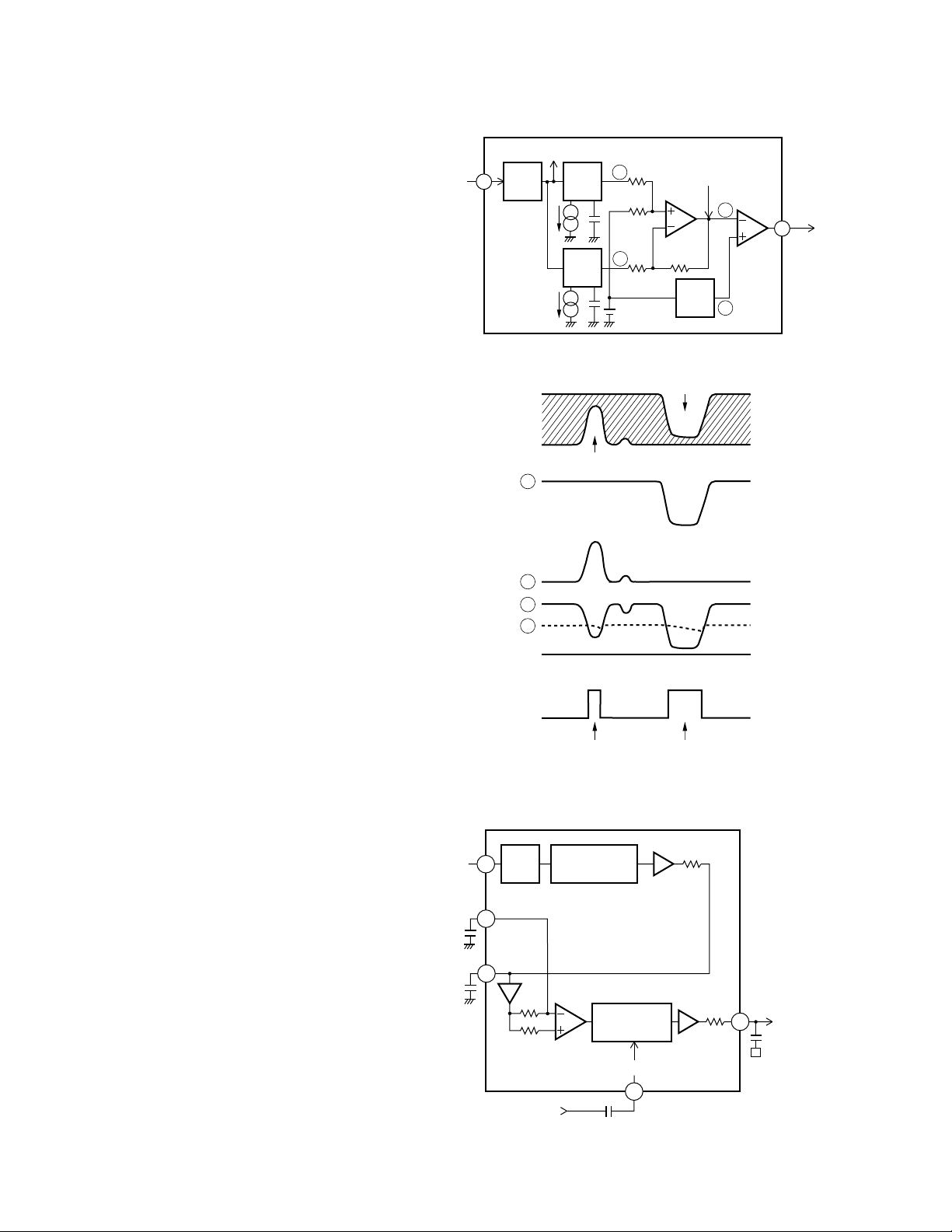
1) Focus servo system
The main equalizer of focus servo is located in the
UPD63702AGF. Fig. 9 shows block diagram of the focus
servo.
For the focus servo system, the lens must be posi-
tioned within the focusing range in order to perform
focus closing. To achieve this, the system moves the
lens upward/downward by focus-search voltage of tri-
angular waveform to detect the focusing point. During
searching, the system kicks the SPDL motor to main-
tain rotation speed to set speed.
The servo LSI monitors FE and RFOK signals so that
focus closing is performed automatically at an appro-
priate point.
Focus closing is performed when the following four
conditions are satisfied:
(1)When the lens moves nearer to the disc.
(2)RFOK = "H"
(3)FZD signal (in IC) is latched to "H"
(4)FE = 0 (REFOUT as reference)
FOCUS
ERROR
D/A
FD
FIN
DRIVER
FOP
FOM
IC301
BA5986FM
LENS
IC 201 UPD63702AGF
76
64
2
4
3
14
13
FOCUS SEARCH
TRIANGULAR WAVE
GENERATOR
DAC
DIGITAL
EQUALIZER
CONTROL
A/D
R301
10kΩ
R302
15kΩ
Fig. 9 Focus servo block diagram
8
CX-890
When the conditions mentioned above are satisfied and
focus is closed, the XSO terminal changes from "H" to
"L". Then, the microcomputer starts monitoring RFOK
signal through L.P.F after 40 ms.
If the system judges RFOK signal as "L", the microcom-
puter takes actions, including protection.
Fig. 10 shows operations related to focus closing. (The
illustration shows when the system cannot perform
focus closing.) S curve, search voltage, and actual lens
behavior can be checked by pressing the Focus Close
button when "01" is shown in Focus Mode Select in Test
mode.
REFOUT
FD
LENS POSITION
RELATIVE TO DISC
NEAR
FAR
"JUST FOCUSED"
SIN
REFOUT
Expanding around "Just Focused Point"
REFOUT
RFI
FOK
FEX
FZD
THRESHOLD
LEVEL
FZD
(INTERNAL SIGNAL)
Focus closing would normally take place at these points
XSO
(IN THE EVENT
FOCUS IS
CLOSED)
LEVEL
Fig. 10 Sequence of Focus Closing
 Loading...