


CX-3158
PIONEER CORPORATION 4-1, Meguro 1-Chome, Meguro-ku, Tokyo 153-8654, Japan
PIONEER ELECTRONICS (USA) INC. P.O.Box 1760, Long Beach, CA 90801-1760 U.S.A.
PIONEER EUROPE NV Haven 1087 Keetberglaan 1, 9120 Melsele, Belgium
PIONEER ELECTRONICS ASIACENTRE PTE.LTD. 253 Alexandra Road, #04-01, Singapore 159936
C PIONEER CORPORATION 2004
K-ZZA. DEC. 2004 Printed in Japan
ORDER NO.
CRT3394
CD MECHANISM MODULE(S10.1AAC)
CX-3158
Model Service Manual CD Mechanism Module
DEH-P770MP/XN/UC CRT3333 CXK5617
DEH-P7700MP/XN/EW CRT3334 CXK5663
DEH-P670MP/XN/UC CRT3335 CXK5663
DEH-3730MP/XN/EW CRT3395 CXK5663
DEH-3700MP/XN/EW
DEH-2750MP/XN/GS CRT3396 CXK5663
DEH-2790MP/XN/ID
DEH-2770MP/XN/CS
DEH-3700MP/XU/UC CRT3397 CXK5668
DEH-4700MP/XU/EW CRT3398 CXK5668
DEH-4700MPB/XU/EW
DEH-3750MP/XU/GS CRT3399 CXK5668
DEH-3770MP/XU/CS CXK5669
DEH-3750MP/XU/CN
DEH-P470MP/XM/UC CRT3400 CXK5668
DEH-P4700MP/XM/UC
DEH-P4750MP/XM/GS CRT3401 CXK5668
DEH-P4790MP/XM/ID
DEH-P4770MP/XM/CS
DEH-P3700MP/XU/UC CRT3402 CXK5668
- This service manual describes the operation of the CD mechanism module incorporated in models list-
ed in the table below.
- When performing repairs use this manual together with the specific manual for model under repair.
CONTENTS
1. CIRCUIT DESCRIPTIONS ...........................................2
2. MECHANISM DESCRIPTIONS.................................19
3. DISASSEMBLY .........................................................21
2
1
234
12
34
F
E
D
C
B
A
CX-3158
1. CIRCUIT DESCRIPTIONS
Recently, most CD LSI's have included DAC, RF amplifier and other peripheral circuits, as well as the core circuit DSP.
This series of mechanisms employ a multi-task LSI UPD63763GJ, which has CD-ROM decoder and MP3/WMA decoder
in addition to the CD block as shown in the Fig.1.0.1. This enables to reproduce a CD-ROM where MP3/WMA data is
recorded.
Fig.1.0.1 Block diagram of CD LSI UPD63763GJ
A-F
UPD63763GJ Audio output
Digital servo
RF amplifier
CD-ROM
decoder
EFM
Signal
processor
Microcomputer
SRAM(1Mbit)
Buffer memory
controller(BMC)
DAC
MP3/WMA
decoder
3
5
6
7
8
F
E
D
C
B
A
5
6
7
8
CX-3158
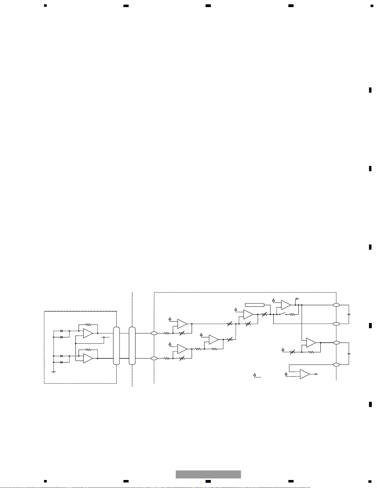
1.1 PREAMPLIFIER BLOCK (UPD63763GJ: IC201)
In the preamplifier block, the pickup output signals are processed to generate signals that are used for the next-stage
blocks: the servo block, demodulator, and control.
After I/V-converted by the preamplifier with built-in photo detectors (inside the pickup), the signals are applied to the
preamplifier block in the CD LSI UPD63763GJ (IC201). After added by the RF amplifier in this block, these signals are
used to produce necessary signals such as RF, FE, TE, and TE zero-cross signals.
The CD LSI employs a single power supply system of + 3.3V. Therefore, the REFO (1.65V) is used as the reference volt-
age both for this CD LSI and the pickup. The LSI produces the REFO signal by using the REFOUT via the buffer amplifi-
er and outputs from the pin 133. All the measurements should be made based on this REFO.
Caution: Be careful not to short the REFO and GRD when measuring.
1.1.1 APC (Automatic Power Control)
A laser diode has extremely negative temperature characteristics in optical output at constant-current drive. To keep
the output constant, the LD current is controlled by monitor diodes. This is called the APC circuit. The LD current is
calculated at about 30mA, which is the voltage between LD1 and V3R3D divided by 7.5 (ohms).
Fig. 1.1.1 APC
PICKUP UNIT CD CORE UNIT
MD
VR
LD-
LD+
5
7
15
14
5
7
15
14
R1
100/16
2SB1132
2R4 x 2
2R7
+
+
-
+
-
+
-
PD
VREF
REG 1.25V
APN
LDS
UPD63763GJ
LD
143
142
6R5K
1K
6R5K
1K
110K
100K
100K
3P
4
1
234
12
34
F
E
D
C
B
A
CX-3158
1.1.2 RF and RFAGC amplifiers
The photo-detector outputs (A + C) and (B + D) are added, amplified, and equalized inside this LSI, and then provided
as the RF signal from the RFI terminal. The RF signal can be used for eye-pattern check.
The low frequency component of the RFO voltage is:
RFO = (A + B + C + D) x 2
The RFO is used for the FOK generation circuit and RF offset adjustment circuit.
The RFI output from the pin 119 is A/C-coupled outside this LSI, and returned to the pin 118 of this LSI. The signal is
amplified in the RFAGC amplifier to obtain the RFAGC signal. This LSI is equipped with the RFAGC auto-adjustment
function as explained below. This function automatically controls the RFO level to keep at 1.5V by switching the feed-
back gain for the RFAGC amplifier.
The RFO signal is also used for the EFM, DFCT, MIRR, and RFAGC auto-adjustment circuits.
Fig. 1.1.2 RF/AGC/FE
PICKUP UNIT
P3
A+C
13
6
13
6
VREF
VREF
125
10K
15R2K
15R2K
R2
VREF
For RFOK generation
To DEFECT/A3T detection
FE A/D
RFOFF setup
61K
61K
8R8K
35K
111K
8R8K
10K
10K
10K
127
128
126
A
B
D
C
B+D
P8
P4
P2
P9
P7
CD CORE UNIT
UPD63763GJ
+
-
+
-
+
-
+
-
RFOFF setup
+
-
136
FEO
135
FE-
+
-
+
-
20K 11R2K
119
RFO
118
AGCI
7R05K
10K 10K
1R2K
5P
5R6K
4R7K
1R2K
33P
56P
123
RF-
122
RF2-
116
AGCO
121
EQ1
120
EQ2
5
5
6
7
8
F
E
D
C
B
A
5
6
7
8
CX-3158
1.1.3 Focus error amplifier
The photo-detector outputs (A + C) and (B + D) are applied to the differential amplifier and the error amplifier to obtain
the (A + C - B - D) signal, which is then provided from the pin 91 as the FE signal.
The low frequency component of the FE voltage is:
FE = (A + C - B - D) x 8.8/10k x 111k/61k x 160k/72k
= (A + C - B - D) x 3.5
The FE output shows 1.5Vp-p S-shaped curve based on the REFO. For the next-stage amplifiers, the cutoff frequency
is 14.6kHz.
1.1.4 RFOK
The RFOK circuit generates the RFOK signal, which indicates focus-close timing and focus-close status during the play
mode, and outputs from the pin 55. This signal is shifted to "H" when the focus is closed and during the play mode.
The DC level of the RFI signal is peak-held in the digital block and compared with a certain threshold level to generate
the RFOK signal. Therefore, even on a non-pit area or a mirror-surface area of a disc, the RFOK becomes "H" and the
focus is closed.
This RFOK signal is also applied to the microcomputer via the low-pass filer as the FOK signal, which is used for pro-
tection and RF amplifier gain switching.
1.1.5 Tracking error amplifier
The photo-detector outputs E and F are applied to the differential amplifier and the error amplifier to obtain the (E - F)
signal, and then provided from the pin 136 as the TE signal.
The low frequency component of the TE voltage is:
TEO = (E - F) x 63k/112k x 160k/160k x 181k/45.4k x 160k/80k
= (E - F) x 4.48
The TE output provides the TE waveform of about 1.3Vp-p based on the REFO. For the next-stage amplifiers, the cut-
off frequency is 21.1kHz.
Fig. 1.1.3 TE
P5
VERF
E
11
F
E
F
9
11
9
P6
P1
P10
130
112K
160K
129
112K
160K160K
63K
80K
161K
45R36K
45R36K
+
-
63K
+
-
+
-
VREF
TEOFF setup
TE A/D
+
-
+
-
+
-
+
-
60K
20K
Inside TEC
139
TEO
138
TE-
140
TE2
141
TEC
47P
6800P
CD CORE UNIT
PICKUP UNIT
UPD63763GJ
6
1
234
12
34
F
E
D
C
B
A
CX-3158
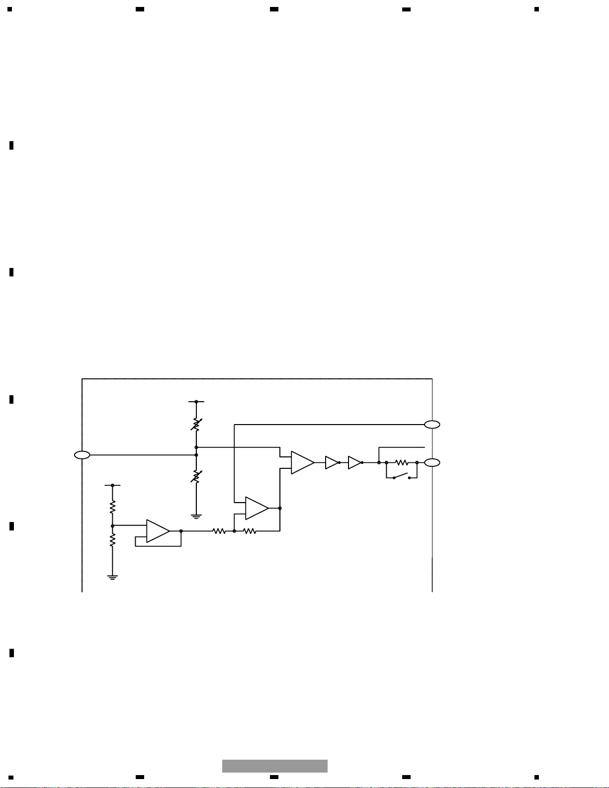
1.1.6 Tracking zero-cross amplifier
The tracking zero-cross signal (hereinafter TEC signal) is obtained by amplifying the TE signal 4 times, and used to
detect the tracking-error zero-cross point.
By using the information on this point, the following two operations can be performed:
1. Track counting in the carriage move and track jump modes
2. Sensing the lens-moving direction at the moment of the tracking close (The sensing result is used for the tracking
brake circuit as explained below.)
The frequency range of the TEC signal is between 300Hz and 20kHz.
TEC voltage = TE level x 4
The TEC level can be calculated at 4.62V. This level exceeds the D range of the operational amplifier, and the signal
gets clipped. However, it can be ignored because the CD LSI only uses the signal at the zero-cross point.
1.1.7 EFM
The EFM circuit converts the RF signal into a digital signal expressed in binary digits 0 and 1. The AGCO output from
the pin 116 is A/C-coupled in the peripheral circuit, fed back to the LSI from the pin 114, and sent to the EFM circuit
inside the LSI.
On scratched or dirty discs, part of the RF signal recorded may be missing. On other discs, part of the RF signal
recorded may be asymmetric, which was caused by dispersion in production quality. Such lack of information cannot
be completely eliminated by this AC coupling process. Therefore, by utilizing the fifty-fifty occurrence ratio of binary
digits (0 and 1) in the EFM signal, the EFM comparator reference voltage ASY is controlled, so that the comparator
level always stays around the center of the RFO signal. The reference voltage ASY is made from the EFM comparator
output via the low-pass filter. The EFM signal is put out from the pin 111.
Fig. 1.1.4 EFM
114
2K
7R5K1R5K
40K
40K
VDD
VDD
+
-
+
-
+
-
RFI
UPD63763GJ
EFM signal
111
EFM
112
ASY
7
5
6
7
8
F
E
D
C
B
A
5
6
7
8
CX-3158
1.2 SERVO BLOCK (UPD63763GJ: IC201)
The servo block controls the servo systems for error signal equalizing, in-focus, track jump and carriage move and so
on. The DSP block is a signal-processing block, where data decoding, error correction, and compensation are per-
formed.
After A/D-converted, the FE and TE signals (generated in the preamplifier block) are applied to the servo block and
used to generate the drive signals for the focus, tracking, and carriage servos.
The EFM signal is decoded in the DSP block, and finally sent out as the audio signal after D/A-converted. In this
decoding process, the spindle servo error signal is generated, supplied to the spindle servo block, and used to gener-
ate the spindle drive signal.
The drive signals for focus, tracking, carriage, and spindle servos (FD, TD, SD, and MD) are provided as PWM3 data,
and then converted to the analog data by the low-pass filter embedded in the driver IC BA5835FP (IC301). These ana-
log drive signals can be monitored by the FIN, TIN, CIN, and SIN signals respectively. Afterwards, the signals are
amplified and applied to each servo's actuator and motor.
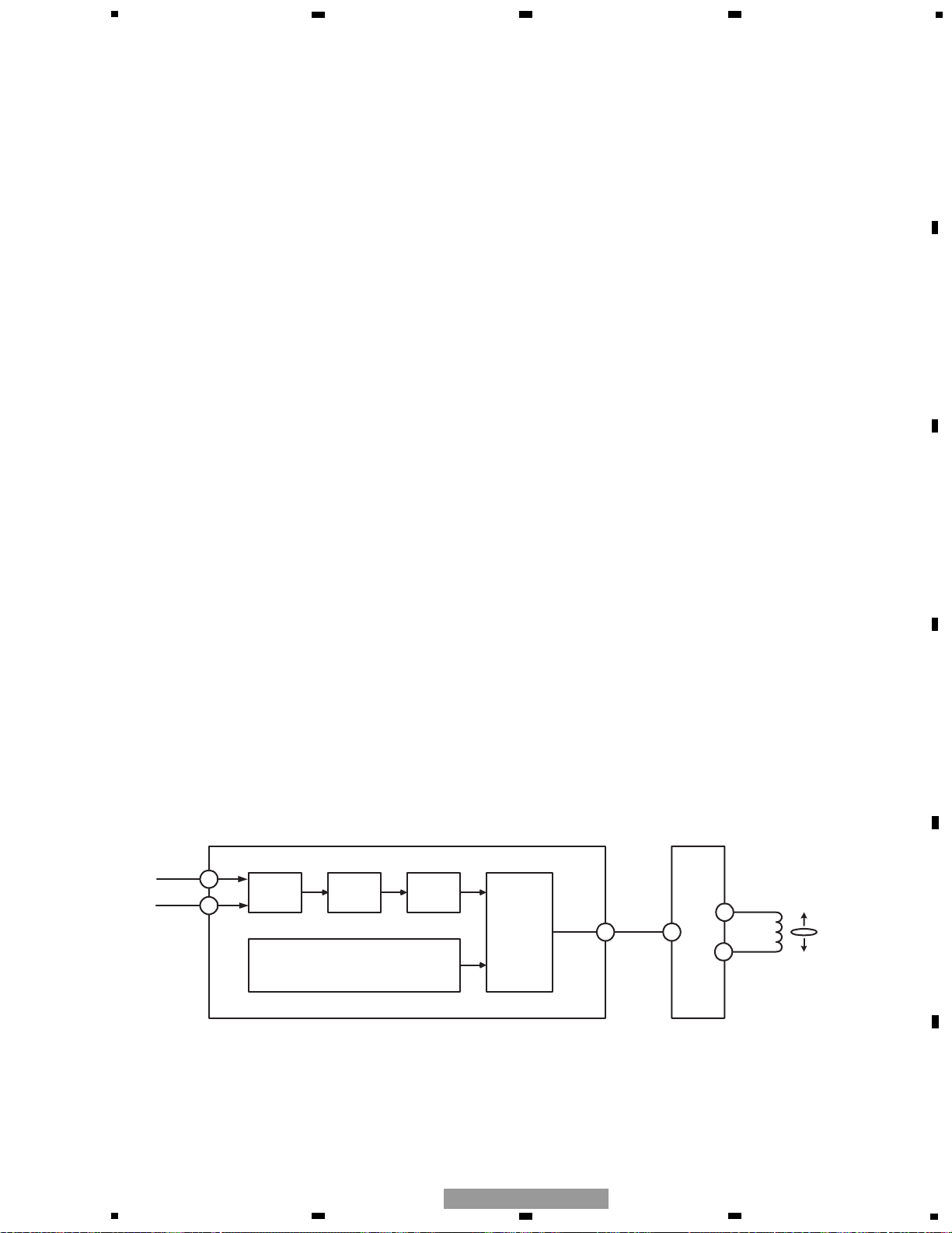
1.2.1 Focus servo system
In the focus servo system, the digital equalizer block works as its main equalizer. The figure 1.2.1 shows the block dia-
gram of the focus servo system.
To close the focus loop circuit, the lens should be moved to within the in-focus range. While moving the lens up and
down by using the focus search triangular signal, the system tries to find the in-focus point. In the meantime, the spin-
dle motor rotation is kept at the prescribed one by using the kick mode.
The servo LSI monitors the FE and RFOK signals and automatically performs the focus close operations at an appropri-
ate timing. The focus loop will close when the following three conditions are satisfied at the same time:
1) The lens moves toward the disc surface.
2) The RFOK signal is shifted to "H".
3) The FE signal is zero-crossed. At last, the FE signal comes to the zero level (or REFO).
When the focus loop is closed, the FSS bit is shifted from "H" to "L". The microcomputer starts monitoring the RFOK
signal obtained through the low-pass filter 10msec after that.
If the RFOK signal is detected as "L", the microcomputer will take several actions including protection.
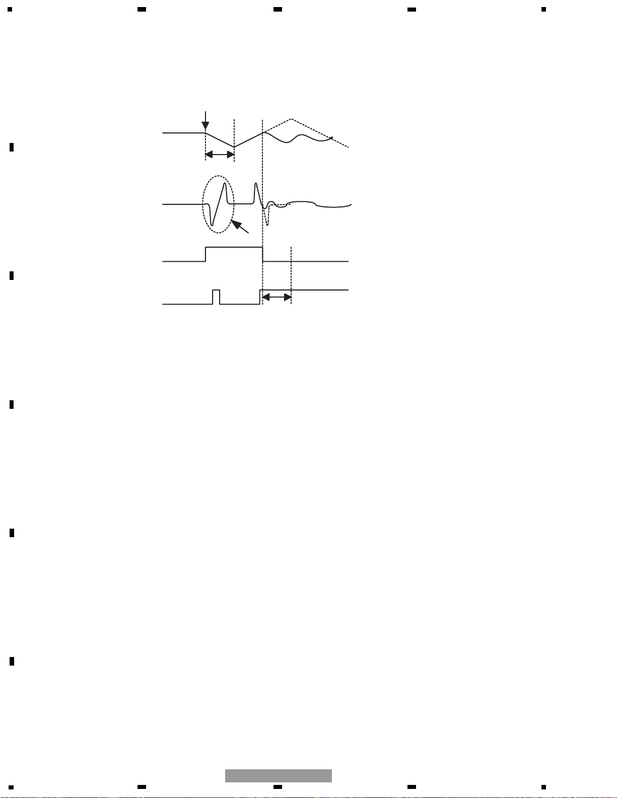
The timing chart for focus close operations is shown in fig. 1.2.2.
(This shows the case where the system fails focus close.)
In the test mode, the S-shaped curve, search voltage, and actual lens movement can be confirmed by pressing the
focus close button when the focus mode selector displays 01.
Fig. 1.2.1 Block diagram of the focus servo system
FE
AMP
A/D
DIG.
EQ
FOCUS SEARCH
TRIANGULAR
WAVE GENERATOR
CONTROL
125
128
A+C
B+D
PWM
FD
UPD63763GJ
6
11
12
FOP
FOM
LENS
BA5835FP
101
8
1
234
12
34
F
E
D
C
B
A
CX-3158
Fig. 1.2.2 Timing chart for focus close operations
1.2.2 Tracking servo system
In the tracking servo system, the digital equalizer block is used as its main equalizer. The figure 1.2.3 shows the block
diagram of the tracking servo system.
(a) Track jump
Track jump operation is automatically performed by the auto-sequence function inside the LSI with a command from
the microcomputer. In the search mode, the following track jump modes are available: 1, 4, and 100
In the test mode, 1, 32, and 32*3 track jump modes, and carriage move mode are available and can be switched by
selecting the mode.
For track jumps, first, the microcomputer sets about half the number of tracks to be jumped as the target. (Ex. For 10
track jumps, it should be 5 or so.) Using the TEC signal, the microcomputer counts up tracks. When the counter
reaches the target set by the microcomputer, a brake pulse is sent out to stop the lens. The pulse width is determined
by the microcomputer. Then, the system closes the tracking loop and proceeds to the normal play. At this moment, to
make it easier to close the tracking loop, the brake circuit is kept ON for 50msec after the brake pulse, and the tracking
servo gain is increased.
In the normal operation mode, the FF/REW operation is realized by continuously repeating single jumps about 10
times faster than the normal single jump operation.
(b) Brake circuit
The brake circuit stabilizes the servo-loop close operation even under poor conditions, especially in the setting-up
mode or track jump mode. This circuit detects the lens-moving direction and emits only the drive signal for the oppo-
site direction to slow down the lens. Thus, this makes it easier to close the tracking servo loop. The off-track direction
is detected from the phases of the TEC and MIRR signals.
FE controlling signals
FSS bit of SRVSTS1 resistor
RFOK signals
Output from FD terminal
A blind period
Search start
You can ignore this for blind periods.
The broken line in the figure is assumed in the case
without focus servo.
The status of focus close is judged from the statuses
of FSS and RFOK after about 10mS.
 Loading...