


TC-P42S2
2010 Plasma TV Technical Guide
2010-Plasma FHD TV – S2 Series (13
Applies to models:
TC-P42S2
th
Generation)
Panasonic National Training
Panasonic Service and Technology Company
TTG100218CP
Prepared by N. Kuge, J. Mizukami, and
Cesar Perdomo.
Edited by Cesar Perdomo
"HDMI, the HDMI logo and High-Definition Multimedia Interface are trademarks or registered trademarks of HDMI Licensing LLC.“
Copyright © 2010 by Panasonic
All rights reserved. Unauthorized copying and distribution is a violation of law.
Warning
This service information is designed for experienced repair technicians only and is not designed for use by the
general public. It does not contain warnings or cautions to advise non-technical individuals of potential dangers in
attempting to service a product. Products powered by electricity should be serviced or repaired only by
experienced professional technicians. Any attempt to service or repair the product or products dealt with in this
service information by anyone else could result in serious injury or death.
Slide 2
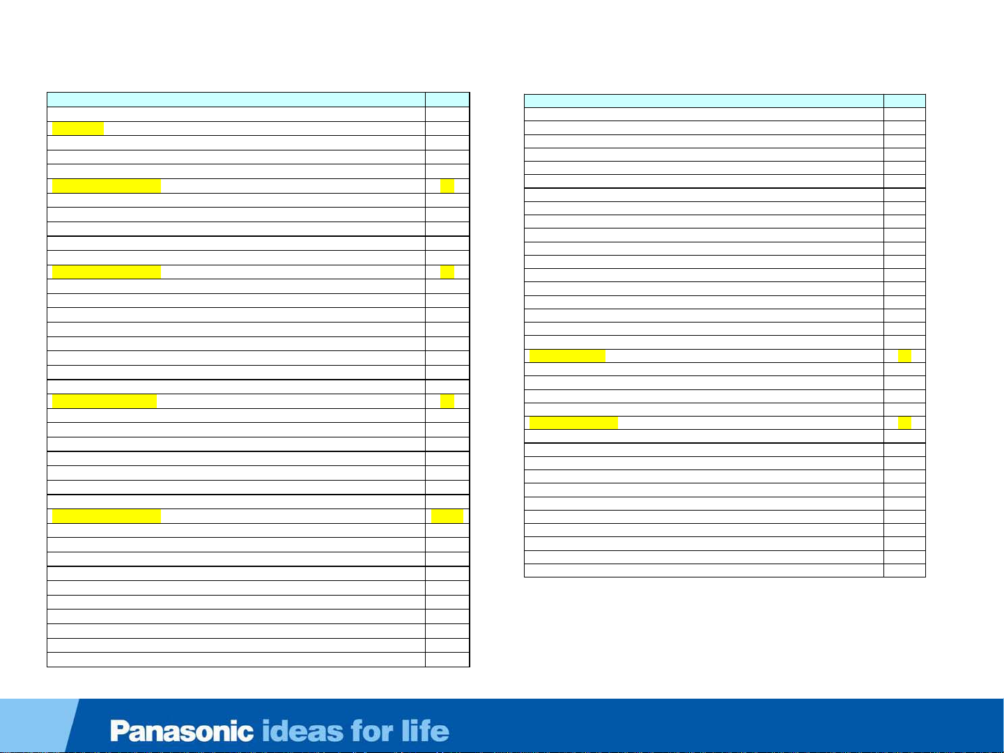
Table of Content
Subject Slide
Table of Contents
Features 5
Series Line up 6
New Features 7
Specifications 8-10
Model Comparison 11
2009/2010 Models Comparison 12-13
Connectors Location (TC-P42S2) 14
Boards Description 15
TC-P42S2 (FHD Model) 16
Technical Changes 17
Start-up Operation 18
Standby/Power On 19
Standby Operation 20
Power On Operation 21
Power On Circuit Explanation 22
CPU Commands Explanation 23
Supply Voltages (SUB Voltages) For Video Processing Circuit 24-28
Overview of Voltage Distribution 29-31
Troubleshooting “No Power” Symptom 32
Signal Processing 33
Signal Process Circuit Comparison between 2009 and 2010 34
Signal Process Circuit 35
Signal Process Circuit Explanation 36
Audio Signal Processing Circuit 37
SOS Detect (Shutdown) 38
Protection circuit block diagram 39
Power LED Error Code Definition 40-41
SOS Detect Circuit 42-43
Panel Drive SOS Detect Block Diagram 44
SOS Detect Circuit 45-46
1 Blink Error Code 47
Troubleshooting 1 Blink Failure 48
2 Blinks Error Code 49
4 Blinks Error Code 56-57
Troubleshooting 4 Blinks Failure (Flowchart) 58
5 Blinks Error Code 59
Troubleshooting 5 Blinks Failure 60-61
Troubleshooting 5 Blinks Failure (Flowchart) 62
6 Blinks Error Code 63
6 Blinks Error Code Circuit Explanation 64
P15V and P5V Test Points (SC Board) 65
Troubleshooting 6 Blinks Failure (Flowchart) 66
7 Blinks Error Detect Circuit 67-68
Troubleshooting 7 Blinks Failure 69
8 Blinks Error Code 70
8 Blinks Error Code Circuit 71
Troubleshooting 8 Blinks Failure (Flowchart) 72
9 Blinks Error Code 73
10 Blinks Error Code 74
10 Blinks Error Detect Circuit 75
Troubleshooting 10 Blinks Failure (Flowchart) 76
Service Notes 77
Service Mode 78
Self Check/Reset 79
Mirror Function 80-81
Vsus Adjustment with Remote Control 82-83
Troubleshooting 84
1st Step Resistance Test – VFG and VFO 85
1st Step Resistance Test – 5V_F and VFG 86
2nd Step – SC Resistance Test 87
2nd Step – SC Resistance Test VFG and TPSC1 88
2nd Step – SC Resistance Test VFG and TPSC1 89
3rd Step SM Resistance 90
3rd Step SM Resistance Test VFG and VFO 91
3rd Step SM Resistance Test VFG and 5V_F 92
SM Board Isolation Procedure 93-95
TV’s Behavior After Connectors Removal 96
Glossary 97-99
Subject Slide
Troubleshooting 2 Blinks Failure 50
Troubleshooting 2 Blinks Failure (Flowchart) 51
3 Blinks Error Code 52
Troubleshooting 3 Blinks Failure 53-54
Troubleshooting 3 Blinks Failure (Flowchart) 55
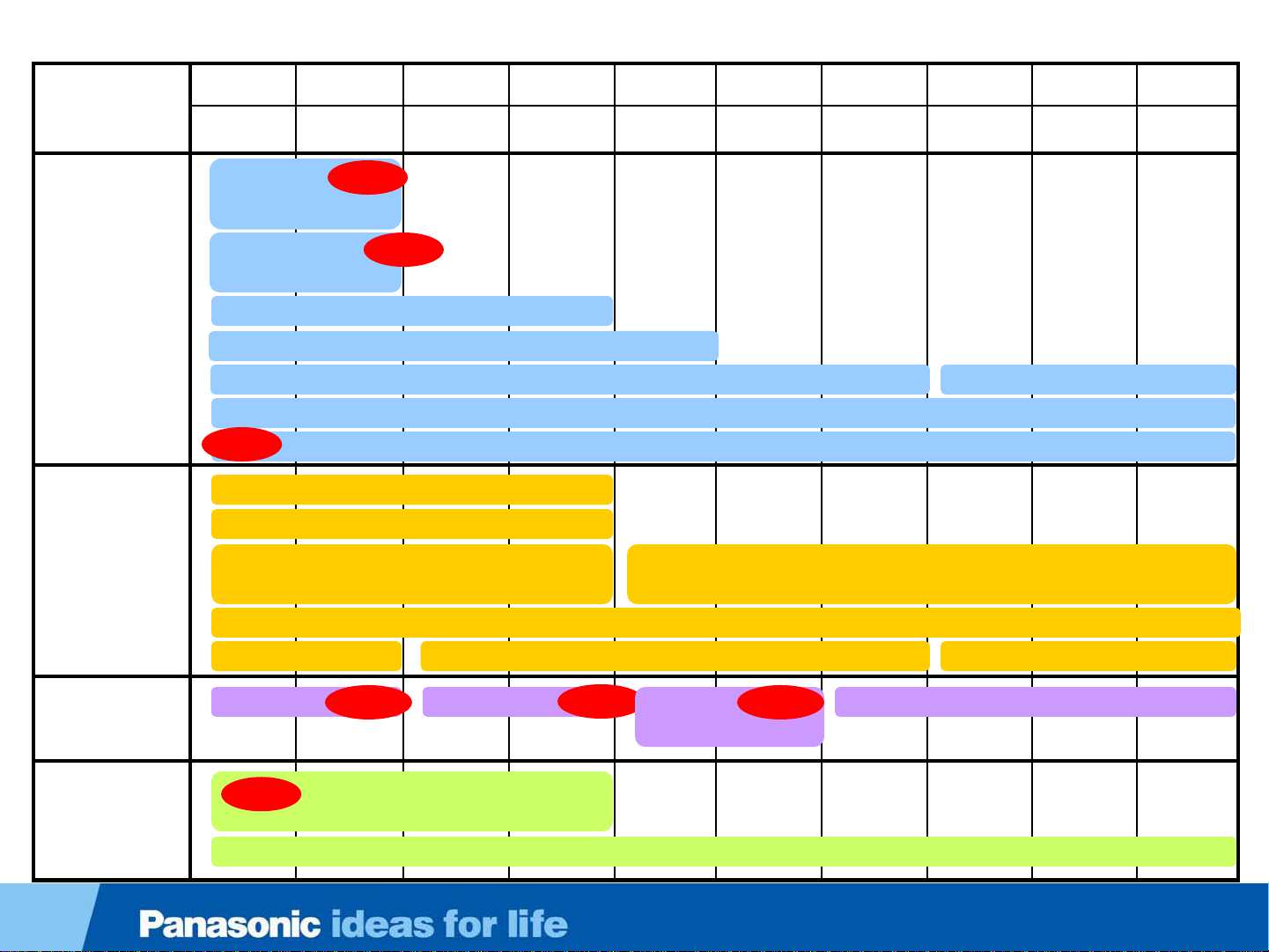
Slide 3

Content
1 - Features
Series Lineup
New Features
Specifications
2 - Models Comparison
Boards Layout
Boards Part Number
Connectors Location
Technical Changes
3 - Start-up Operation
STB Operation
Power On Operation
4 - SOS Detect Circuit with Troubleshooting Flowcharts
5 - Video Signal Process Circuit/Panel Drive Operation
6 - Service Notes
Service Mode
Self-check
Reset
Aging Mode
7 - Troubleshooting
Boards Isolation Procedure
TV’s Behavior After Connectors Removal
Slide 4

Features
Slide 5

Series Line up
SERIES MODELS
42” 46” 50” 54” 58” 65”
VT SERIES
(FHD Premium 3D)
G SERIES
(FHD Core)
S SERIES
(FHD Leader)
PS,U SERIES
(FHD Entry)
X SERIES
(HD Leader)
PX,C SERIES
(HD Entry)
TC-P50VT25
TC-P50VT20
TC-P50G25
TC-P42G25 TC-P46G25
TC-P42S2 TC-P46S2 TC-P50S2 TC-P54S2 TC-P58S2 TC-P65S2
TC-P42U2
TC-P42X2 TC-P50X2
TC-42PX24
TC-P42C2
TC-P46C2
TC-P50G20
TC-50PS24
TC-P50U2
TC-50PX24
TC-P50C2
TC-P54VT25 TC-P58VT25 TC-P65VT25
TC-P54G25
TC-P54G20
TC-58PS24 TC-65PS24
Slide 6
New Features
VT25 VT20 G25 G20 S2 PS24 U2 X2 PX24 C2
Clubs Clubs
High
Picture
Quality
Smart
Networking
FHD 3D
NEW
Dual Scan
Short Stroke
Phosphor
NEW
THX Certified
Moving Picture 1080 Lines
1080p 720p
600Hz Sub-field Drive
NEW
Infinite Black Plus (Native CR > 2 Mil:1)
Viera Cast IPTV
Wi-Fi Ready (USB)x2
VIERA Image Viewer
Image Viewer (Photo only)
(Movie & Photo)
VIERA Link
4 HDMI 3 HDMI 2 HDMI
Stylish
Design
Environmen
tally
Friendly
Metallic
NEW
NEW
Buck Cut
Energy Saving
(Louver Filter)
Mercury & Lead Free + 100,000 hrs + Eco Mode
Slide 7
NEW
Glossy
NEW
& Pattern Texture
Glossy
Slide 7
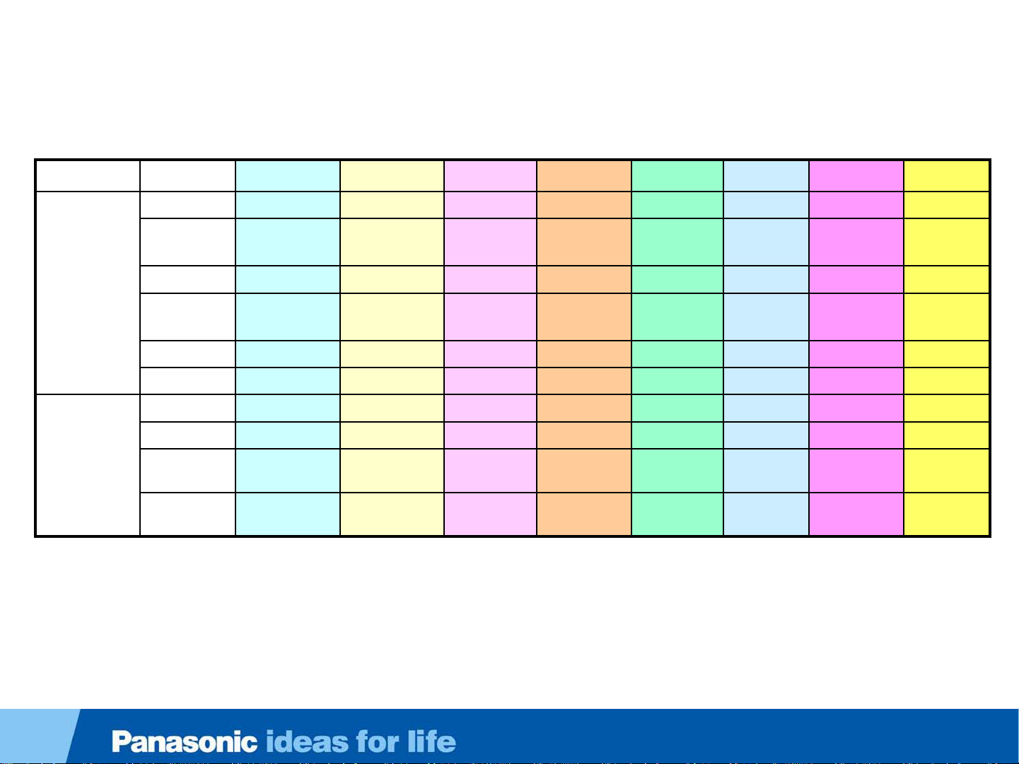
Specifications (1 of 3)
VT SERIES G SERIES S SERIES PS SERIES U SERIES X S E RIES PX SERIES C SERIES
Main
Specification
Picture Deep Color
Resolution
Contrast
(Native)
Gradation
Filter
Remote
THX
X.V. Color
Game
Mode
Motion
Reality
1920X1080 1920X1080 1920X1080 1920X1080 1920X1080 1024X768 1024X768 1024X768
Infinite:1 Infinite:1 Infinite:1 Infinite:1 Infinite:1 Infinite:1 Infinite:1 Infinite:1
6144 6144 6144 6144 6144 6144 6144 6144
Louver
(Direct filter)
w/ Viera Cast w/ Viera Cast - - - - - Y Y N N N N N N
Y Y Y Y Y Y Y Y
Y Y Y Y Y Y Y Y
Y Y Y N Y Y N N
1080 lines 1080 lines 1080 lines 900 lines 720 lines 720 lines 720 lines 720 lines
Louver
(Direct filter)
AR AR - AR AR -
Slide 8

Specifications (2 of 3)
VT SERIES G SERIES S SERIES PS SERIES U SERIES X SERIES PX SERIES C SERIES
Sound Surround
Sound Control
BBE
Balance Control
Lip Sync
Improvement
Terminal
Input
AV1 Type
(Position)
AV2 Type
(Position)
Component1
Type (Position)
Component2
Type (Position)
HDMI1 Position
HDMI2 Position
HDMI3 Position
Y Y Y Y Y Y Y Y
Y Y Y Y Y Y Y Y
Y N N N N N N N
Y Y Y Y Y Y Y Y
Y Y Y Y Y Y Y Y
RCA/S
(Rear)
RCA
(Side)
RCA
(Rear)
RCA
(Rear)
Rear Rear Rear Rear Rear Rear Rear Rear
Rear Rear Rear Rear Rear Rear Rear Rear
Rear Side Side Side Side - - -
RCA/S
(Rear)
RCA
(Side)
RCA
(Rear)
RCA
(Rear)
RCA/S
(Rear)
RCA
(Side)
RCA
(Rear)
RCA
(Rear)
RCA/S
(Rear)
RCA
(Side)
RCA
(Rear)
RCA
(Rear)
RCA/S
(Rear)
RCA
(Side)
RCA
(Rear)
RCA
(Rear)
RCA/S
(Rear)
RCA
(Side)
RCA
(Rear)
RCA
(Rear)
RCA/S
(Rear)
RCA
(Side)
RCA
(Rear)
RCA
(Rear)
RCA/S
(Rear)
RCA
(Side)
RCA
(Rear)
RCA
(Rear)
HDMI4 Position
PC Input
Terminal
Output
Network Ethernet
Digital Audio
Out
Side - - - - - - 1 1 - 1 - 1 Y Y Y Y Y Y Y Y
1 1 - - - - - -
Slide 9
Specifications (3 of 3)
VT SERIES G SERIES S SERIES PS SERIES U SERIES X SERIES PX SERIES C SERIES
Card I/F SD Card Slot
SD Card LED Color
SD Function
Other I/F USB
(Wi-Fi Ready)
RS-232C
Function DLNA
IPTV
Y Y Y Y Y Y Y Y
Blue - - - - - - Movie &
Photo
2 2 - - - - - -
1 - - - - - - -
- - - - - - - Viera Cast Viera Cast - - - - - -
Movie &
Photo
Photo Photo Photo Photo Photo Photo
Slide 10

Models Comparison
Slide 11
2009/2010 Models Comparison (1 of 2)
2009 model 2010model New features Remarks
3D Added(120kHz frame sequential)
Panel NeoPDPeco Panel
Native contrast Infinite:1
TC-P**V10 TC-P**VT25/20
TC-P**G10/15 TC-P**G25/20
TC-P**S1 TC-P**S2
Screen coating Louver (Direct filter, No front glass)
USB Added (Wi-Fi Ready)
Power Consumption -40%
Panel NeoPDPeco Panel
Native contrast Infinite:1
Screen coating Louver (Direct filter, No front glass)
Power Consumption -40%
Panel NeoPDPeco Panel
Native contrast Infinite:1
X.V. Color Added
Power Consumption -40%
TC-**PS14 TC-**PS24
Panel NeoPDPeco Panel
Native contrast Infinite:1
Gradation 6,144
X.V. Color Added
Power Consumption -40%
Slide 12
2009/2010 Models Comparison (2 of 2)
2009 model 2010model New features Remarks
Panel NeoPDPeco Panel
Native contrast Infinite:1
Gradation 6,144
TC-P**U1 TC-P**U2
X.V. Color Added
Game mode Added
Power Consumption -40%
TC-P**X1 TC-P**X2
TC-P**X14 TC-P**PX24
TC-P**C1 TC-P**C2
Panel NeoPDPeco Panel
Resolution 1024X768 (*1)
Native contrast Infinite:1
Gradation 6,144
X.V. Color Added
HDMI input 2 (*2)
Power Consumption -40%
Panel NeoPDPeco Panel
Resolution 1024X768 (*1)
Native contrast Infinite:1
Gradation 6,144
X.V. Color Added
Power Consumption -40%
Panel NeoPDPeco Panel
Resolution 1024X768 (*1)
Native contrast Infinite:1
Gradation 6,144
Power Consumption -40%
(*1)2009
model is
1,366 x 768.
(*2)2009
model is 3.
(*1)2009
model is
1,366 x 768.
(*1)2009
model is
1,366 x 768.
Slide 13

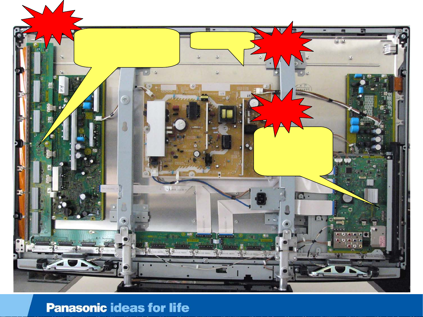
Connectors Location (TC-P42S2)
Slide 14
Boards Description
Board Description Board Description
A Speaker out, Sound Processor, AV Terminal, AV
Switch, DC-DC Converter, Digital Signal
Processor, Microcomputer, HDMI Interface, SD
card slot, Format-Converter, Plasma AI, Sub-
Field Processor, ( Newly Added Key Switch )
C1 Data Drive ( Right ) SC Scan Drive
C2 Data Drive ( Left ) SU Scan Out ( Upper )
K Remote Receiver, Power LED SD Scan Out ( Lower )
P Power Supply
42” SM
Boards comparison between 2009 S1 series and 2010 S2 series
2009
⇒
S1 series
SU + SD SM ( only 42inch )
⇒
2010
S2 series
Board
GK + S Delete ( on A board )
⇒
Slide 15
New
TC-P42S2 (FHD Model)
( 42inch only )
SU and SD board are
integrated to SM board
No fans
New
New
Power SW and
Key Input are
now on the A
board
Slide 16

Technical Changes
The resolution of the 50” HD models has been reduced from 1,366x768 to 1024x768 (Same as the 42”
HD models).
TC-P42S2
The Power Switch is located on the A board (G20 and S2 models). The U2, X2, and C2 models still
have the power switch on the S board.
The SU and SD boards are now just one board (SM). The TC-P42X2 model combines the SU, SD, and
SC boards into just on board (SN).
Instead of 30V, SUB5V is used as the Tuner +B. The tuner has a built-in DC-DC Converter.
P5V is produced in the A board. (Not in the P board.)
The Main CPU and the Front end processor circuit are built into one IC. (Nile-TCON IC8001).
IC8001 uses STB3.3V and STB1.2V as VCC.
Vset is no longer used on the SC board.
P25/A25 connector is deleted
G20/25, VT20 Series
No front glass is used on these models.
Slide 17

Start-up Operation
Standby/Power On
Slide 18
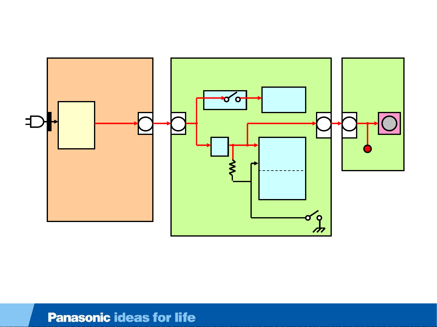
Standby Operation
P9
P
P
Circuit
STB
STB5V
P7
1 1
5V
A7
3.3V
REG
STB5V
3.3V
REG
3.3V
3.3V
POWER SWITCH
IC9003
PANEL
Vcc
Vcc
Processing
CPU
STB3.3V
MAIN
CPU
Signal
IC8001
A
A
A1 K1
3 3
K
K
REMOTE
REC.
LED
Slide 19

Standby Circuit Explanation
When the TV is plugged in:
AC is applied to the standby circuit in the power supply to produce STB5V.
The STB5V is provided to the A board via connectors P7 (Pin 1).
The STB5V from pin1 of connector P7 is applied to a 3.3V regulator to power the Main CPU
(IC8001) on the A board. This energizes and prepare the microprocessor (CPU) for program
execution.
The 3.3V from the voltage regulator besides being applied to the CPU, is also applied to the
remote control receiver and the power LED on the K board through connector A1/K1 (pin 3).
If the STB5V is missing, the TV is dead (No power)
Slide 20
Power On Operation
P9
P
P
RELAY
STB
Circuit
Vsus, Vda
STB5V
Power
CPU
F15V
P15V
P7 A7
7 7
55
3.2V
3.2V
TV_SUB_ON
SUB3.3V,
1.8V,1.2V
3.2V
5V
1 1
P6 A6
77
88
PA4701
99
14.6V
F15V
PANEL_MAIN_ON
IC9004
3.3V
REG
PANEL_STB_ON
STB5V
IC4700(A)
3.3V
REG
IC5606
IC5610
3.3V
STB3.3V
3.3V
10 blinks
SOS Detect
SUB1.8V
SUB1.2V
SUB5V
IC9003
PANEL
Vcc
Vcc
KEY_INPUT
Processing
CPU
IC8001
MAIN
Signal
IC4700(B)
IC4700(B)
Detect
A
CPU
TUNER
A
A1 K1
3 3
6
5 5
Voltage Drop
Error Detect
K
K
6
POWER
SWITCH
REMOTE
REC.
LED
IC5608
SUB3.3V
SUB3.3V
Slide 21

Power On Circuit Explanation
The power command from the power switch on the A board or the remote control
receiver on the K board is provided to the Main CPU on the A board (IC8001).
The CPU on the A board outputs the “TV_SUB_ON” Command (3.2V) and the
PANEL_STB_ON” command (3.2V).
The “TV_SUB_ON” command is provided to pin 5 of connector P7 of the power supply
to develop the F+15V. At this time, the relays on the power supply are triggered and a
“click” sound can be heard.
The F+15V from the P board is applied to several voltage regulator (IC5608- IC5610, and
IC5606) on the A board. The voltage output from these ICs are SUB5V, SUB1.8V,
and SUB1.2V respectively. They are used by various circuits on the A board.
To avoid catastrophic failures, they are monitored by an SOS Detect circuit (IC4700) for
over-voltage and over-current conditions. Any abnormalities of the SUB5V,
SUB1.8V, or SUB1.2V triggers the SOS circuit. The TV shuts down and the power LED
blinks 10 times.
The “PANEL_STB_ON” is used to turn on the 3.3V regulator (IC9004) on the A board.
The output voltage is applied to the “Panel CPU” on the A board. The Panel CPU on the
A board outputs the “PANEL_MAIN_ON” Command (3.2V) to pin 7 of connector P7 on
the P board. The “PANEL MAIN ON” command turns on the power supply circuit that
outputs the Vsus, Vda, and 15V.
Slide 22
CPU Commands Explanation
TV SUB ON (F-STBY-ON), PANEL-STB-ON, PANEL MAIN ON, and DISPEN.
The “TV Sub On”
The CPU on the A board outputs the
“TV_SUB_ON” Command (3.2V) when the
power is turned on. This command is used to
turn on the circuit in the power supply that
generates the F+15V.
The F+15V is provided to the A to generate the
Sub-voltages used by the signal process
circuit.
When the output of the Sub-voltages is
confirmed by the system MPU, it outputs the
“Panel STB On” command.
The “Panel STB On” (3.2V) command is used
to energize the panel MPU IC. When the panel
MPU is energized, it outputs the “Panel Main
On” command.
A7
A
5
7
PANEL_MAIN_ON
TV_SUB_ON
IC9004
RESET
RESET
3.3V
3.3V
IIC-SW
IIC-SW
P_ON/OFF
IC9003
panel
pane
uCOM
uCOM
l
IC8001-2
Nile-
Nile-
TCON
TCON
(SYSTE
(SYSTE
M CPU)
M CPU)
DISPEN
The “Panel Main On” (3.2V) command is
applied to the power supply to turn on the
circuits that generate the Vsus, Vda, P15V.
The “Dispen” (Display Enable) command is
applied to the Discharge Control/Sub-field
Conversion IC (IC9300) to begin panel drive
operation and video display.
PANEL_STBY_ON
PANEL_VCC_ON
Slide 23

P
STB5V
P7
Supply Voltages (Sub Voltages) For Video Processing Circuit
A7
5
5
IC4700
1
1
STB5V
1
RESET
RESET
3.3V
3.3V
TV_SUB_ON
MCU_XRST (STB_RST )
3
2
STB3.3V
IC5601
STB reset
STB reset
5
4
IC8001-1
Nile-TCON
Nile-TCON
(SYSTEM
(SYSTEM
CPU)
CPU)
A
F+15V
P6
5V
IC8004
EEPROM
EEPROM
IC8502
Flash ROM
Flash ROM
IC8002
DDR2
DDR2
SUB5V
IC5609
3.3V
IC5607
3.3V
IC5605
3.3V
IC5613
3.3V
Power
Switch
DDR_VCC_POST
=SUB1.8V
SUB1.2V
SUB3.3V_A
3.3V
SUB3.3V_HDMI
3.3V
SUB3.3V
3.3V
SUB3.3V_SD
3.3V
SUB5V
STB3.3V
SUB3.3V
IC2106-1
AMP
AMP
IC8503
EEPROM
EEPROM
IC4701
TEMP sense
TEMP se
JK8502
4
TU8302
TUNER
TUNER
LED/
Remote
A1
3
1
nse
SD card
SLOT
IC9004
RESET
A6
A6
7
7
8
8
9
9
#
= Steps
F+15V
6
RESET
3.3V
3.3V
IIC-SW
IIC-SW
PA4701
(Fuse)
F15V
IC5610
1.8V
1.8V
IC5606
1.2V
1.2V
IC5608
5V
SUB5V /
SUB5V_TUNER
Sub-Voltages Distribution Explanation
AC is applied to the standby circuit in the power supply to produce STB5V when the TV is plugged in.
The STB5V is provided to the A board via connectors P7 (Pin 1).
1
2
3
The power command from the power switch on the A board or the remote control receiver
4
The CPU on the A board outputs the “TV_SUB_ON” Command (3.2V)
5
The F+15V from the P board is applied to several voltage regulator (IC5608- IC5610, and
6
The STB5V from pin1 of connector P7 is applied to a 3.3V regulator to power the Main
CPU (IC8001) on the A board. This energizes and prepare the microprocessor (CPU)
for program execution.
The 3.3V from the voltage regulator besides being applied to the CPU, is also applied to the
remote control receiver and the power LED on the K board through connector A1/K1 (pin 3).
The reset pulse from IC4700 is applied to the Main CPU (IC8001) for program execution.
on the K board (Not shown on the schematic) is provided to the Main CPU on the A board
(IC8001).
The “TV_SUB_ON” command is provided to pin 5 of connector P7 of the power supply
to develop the F+15V. At this time, the relays on the power supply are triggered and a
“click” sound can be heard.
IC5606) on the A board. The voltage output from these ICs are SUB5V, SUB1.8V,
and SUB1.2V respectively. These voltages are used by the signal processing circuit in the
A board.
The circuit responsible for processing the signal is now ready. All the necessary voltages are present.
Slide 25
P
STB5V
SND15V
P15V
11a
11b
VSUS
Vda
Supply Voltage (P15V) For 1
A7
P7
5
5
IC4700
RESET
RESET
3.3V
IC9004
RESET
RESET
3.3V
3.3V
IIC-SW
IIC-SW
3.3V
3.3V
CE(STB_D3.3V output)
DCDC_OE
13
P6
1
1
7
7
A6
1
1
2
2
3
3
A20
29
30
1
STB5V
IC2106-2
AMP
AMP
P15V
P15V
P15V
P5V
10
PANEL_MAIN_ON
SND15V
11
st
Stage of Panel Drive Circuit
TV_SUB_ON
MCU_XRST (STB_RST )
STB3.3V
IC9003
9
12
NRST
P_ON/OFF
STB_D3.3V
uCOM
8
IC9001
EEPROM
EEPROM
IC9803
3.3V
3.3V
IC9800
1.2V
1.2V
IC9801
5V
5V
P5V /
P5V_DCDC
panel
panel
uCOM
P3.3V
P3.3V
P1.2V
PANEL_READY
XRST
DRVRST
PANEL_STBY_ON
P3.3V
IC9400
Buffer
Buffer
IC9401
Buffer
IC8001-2
16
14
15
/PANEL_VCC_ON
IC9304
EEPROM
EEPROM
IC9300
Discharge control
Discharge control
Sub-field Conv.
Sub-field Conv.
IC9402
Buffer
Buffer
Buffer
Nile-
Nile-
TCON
TCON
(SYSTEM
(SYSTEM
CPU)
CPU)
7
DISPEN
17
Panel drive /
Picture signal
18
A
A31
66
67
68
66
68
A32
Panel Drive Circuit Supply Voltages
When the output of the Sub-voltages is confirmed by the system MPU,
7
The System CPU outputs the “Panel STB On/Panel VCC On” command to IC9004.
8
9
10
11
12
13
14
15
When Panel STB On command is applied to IC9004, STB3.3V is developed.
Reset (NRST) is also generated by IC9004
When STB3.3V and Reset are applied to the Panel CPU (IC9003), the PANEL MAIN
ON command is output to the power supply.
P15V is output from the power supply when it receives the PANEL MAIN ON command.
Vsus and Vda are also output at this point.
11b11a
Right after the PANEL MAIN ON command is output from IC9003, the P_ON/OFF
command is also output to IC9004.
IC9004 outputs the ENABLE command to the voltage regulators IC9800, 9801, 9803 to
output 3.3V, 1.2V, and 5V respectively.
IC9003 also outputs XRST
IC9003 outputs DRVRST (Drive Reset) to reset the drive section of IC9300 and begin
panel drive operation.
16
17
18
PANEL READY from the Panel CPU is output to the System CPU to signal the
beginning of panel drive operation.
IC8001 outputs the DISPEN (Display Enable) command to IC9300 to begin panel drive
and picture drive operation.
IC9300 outputs the pulses and data necessary to drive the panel and generate video.
Slide 27

Supply voltages (Vsus and Vda) for 2
When the Vsus, Vda, and P15V and all its derivates voltages are present, the panel drive circuit starts to
operate.
AC in
nd
Stage of Panel Drive Circuit
TC-P42S2
Relay
Power factor
control
SC SS
Vsus
P35
Vda
Vda
1
2
P11
1
SS11
1
SC2
Vsus
P2
11
VSUS
11a
Vda
11b
C1
Vda
C10 C20
1-5
16-20
Vsus
Vda
C25
Vda
1-2
C2
Slide 28
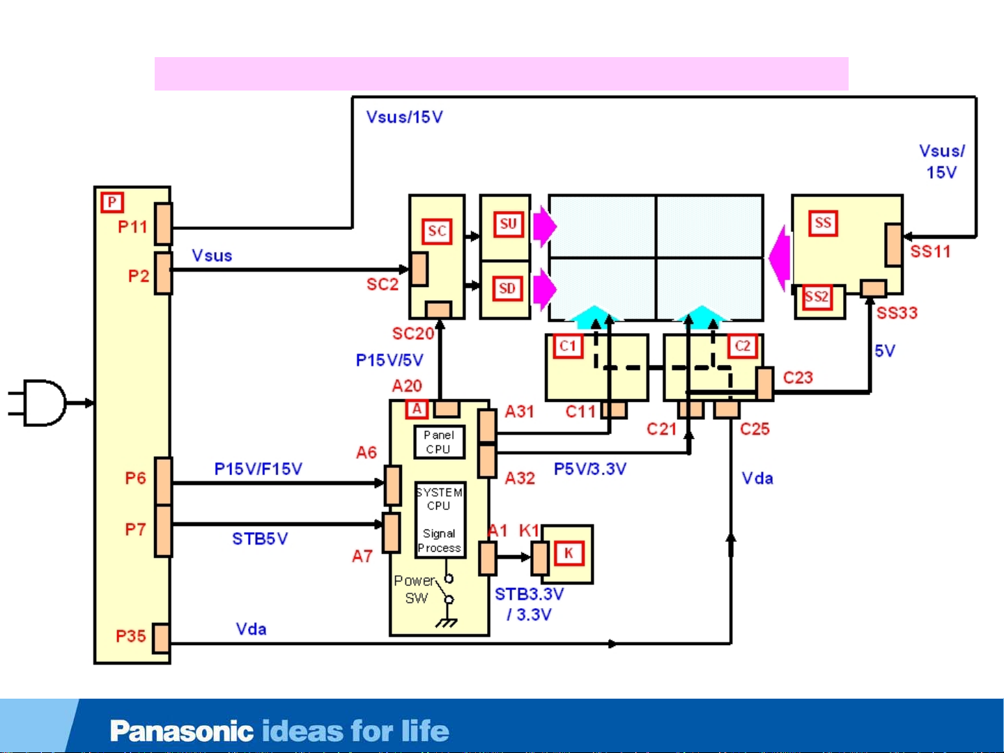
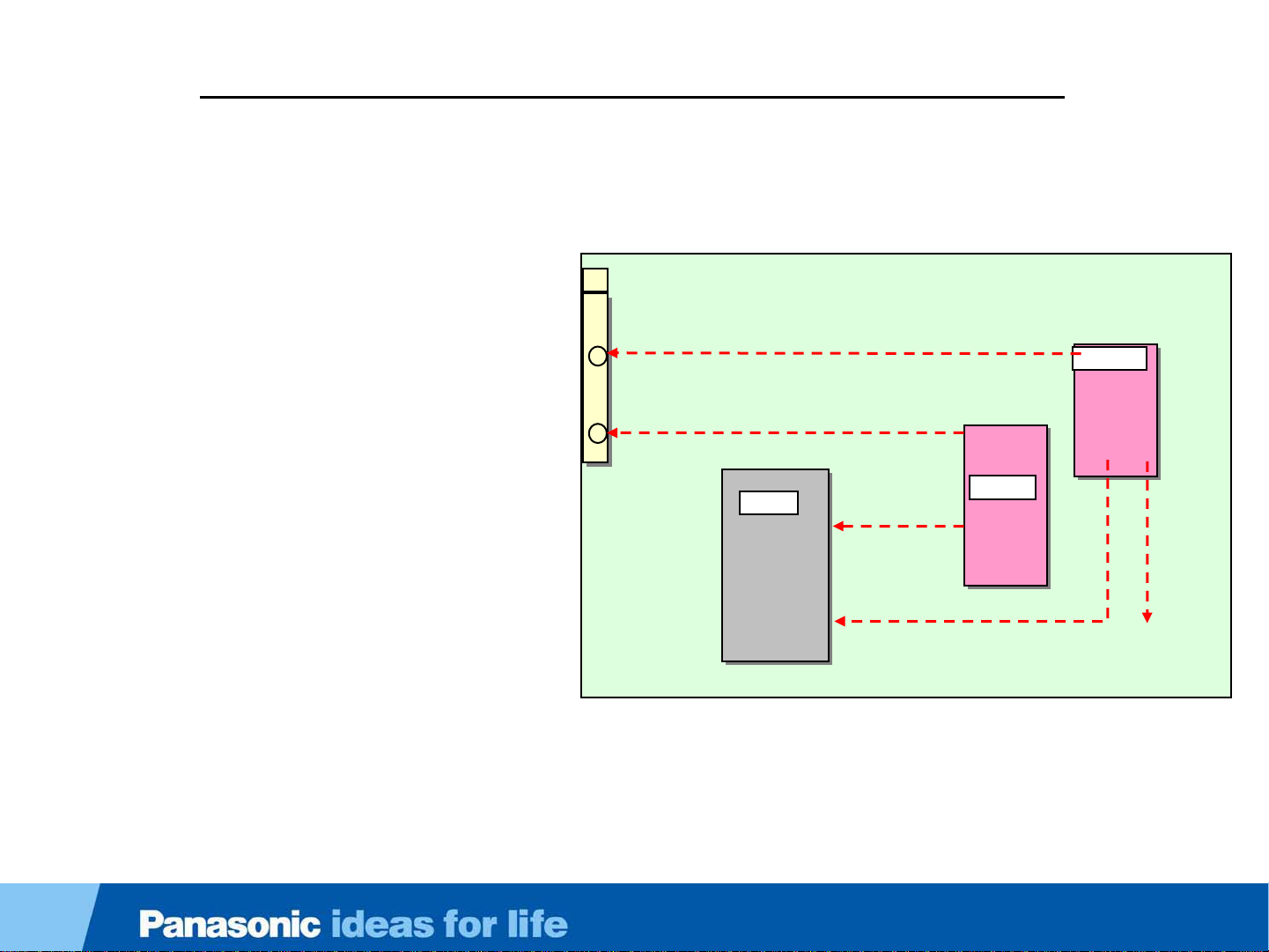
Overview of Voltage Distribution
The voltage distribution to all the boards is illustrated in this block diagram
P3.3V
Drawing is
46inch
50inch: C1-C2 → C1-C3
42inch: SU+SD → SM )
Slide 29

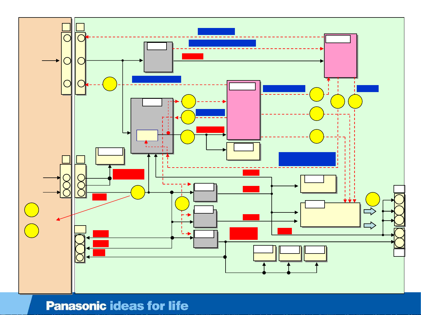
AC input
SU
TC-P42S2
The voltage distribution
to all the boards is
illustrated in this block
diagram
SC
DCDC
DCDC
DCDC
5V
SC2
Vsus
(P34)
P6
A6
Power
uCOM
F_STBY
F15V
Stand-by
power
REG
15V
P7
A7
STB5V
STB 5V
Relay
Power factor
control
15V
DC/DC
15V
Vsus
Vsus
Vda
P35
Vda
P11P2
15V
SC11
SS
DCDC
5V
SD
C1
SC20
15V
5V
A20
F15V
A31
C11
5V
3.3V
3.3V
3.3V
STB3.3V
A32
5V
C21
A
Vda
C25
SS33
5V
C23
C2
Slide 30
 Loading...