


Panasonic Service and Technology Company
Technical Guide
TC-32LX70/700, TC37LZ85, and TC-32LX85 LCD Display Television
National Training

Prepared by
Jean Magloire
Panasonic Service and Technology Company
National Training
Copyright © 2008 by Panasonic Services Company
All rights reserved. Unauthorized copying and distribution is a violation of law.
Warning
This service information is designed for experienced repair technicians only and is not designed for use by the general public. It does not contain warnings or cautions to advise non-technical individuals of potential dangers in attempting to service a product. Products powered by electricity should be serviced or repaired only by experienced professional technicians. Any attempt to service or repair the product or products dealt with in this service information by anyone else could result in serious injury or death.

Table of Contents
|
Subject |
Page # |
Subject |
Page # |
|
|
|
|
|
Topics |
|
5 |
Self-Check Menu |
38 |
|
|
|
|
|
2007 LCD TV Specifications |
7 |
Check Point |
39 |
|
|
|
|
|
|
P.C.B Layout (LX700) |
8 |
Serviceman Mode |
40 |
|
|
|
|
|
|
P.C.B Layout |
(LX70) |
9 |
Serviceman Mode Menu and Navigation |
41 |
|
|
|
|
|
P.C.B Layout |
(LX700 Pictorial) |
10 |
Adjustment Data |
42 |
|
|
|
|
|
P.C.B Layout |
(LX700 Connectors) |
11 |
SRV-TOOL |
43 |
|
|
|
|
|
P.C.B Layout |
(LX700 LVDS Connector) |
12 |
Voltage chart of AP-board |
45 |
|
|
|
|
|
TC-32LX700 Board Description |
13 |
Voltage chart of P and A boards |
46 |
|
|
|
|
|
|
P Board – Main Power Board |
15 |
Voltage chart of DT board |
47 |
|
|
|
|
|
|
Main MPU (Power On Commands) |
17 |
Troubleshooting Signal Problems |
49 |
|
|
|
|
|
|
Standby Operation |
19 |
Picture NG and Sound OK (LX700/LX70 ) |
50 |
|
|
|
|
|
|
SUB Voltages and Over-voltage Protection |
21 |
Picture OK and Sound NG (LX700/LX70) |
51 |
|
|
|
|
|
|
Main Voltages and Over-voltage Protection |
22 |
Picture NG and Sound NG (LX700/LX70 ) |
52 |
|
|
|
|
|
|
Inverter_On Command and Protection |
23 |
No Picture from TV Reception |
53 |
|
|
|
|
|
|
Video Process Block Diagram |
25 |
No Picture |
54 |
|
|
|
|
|
|
Audio Process Block Diagram |
27 |
No Video, Dark Blue Screen |
55 |
|
|
|
|
|
|
MPU SOS Inputs and Blink Codes |
29 |
No Audio |
57 |
|
|
|
|
|
|
Over-Current Protection Circuit |
31 |
No Power |
58 |
|
|
|
|
|
|
Over-Current Protection Circuit 2 |
33 |
Power LED Blinks One Time (INV_SOS) |
60 |
|
|
|
|
|
|
Power LED Timing Table |
35 |
Power LED Blinks Three Times (TV_SOS) |
61 |
|
|
|
|
|
|
Self-Check and Reset Function |
37 |
Power LED Blinks Four Times |
62 |
|
|
|
|
|
|
3

TablePurposelyof ContentsLeft Blank
2008 LCD Television Models |
63 |
|
|
Full HD TC-LZ85 & HD TC-LX85 Series |
64 |
|
|
Chassis structure (37 Full HD type) |
65 |
|
|
Chassis structure (37 HD type) |
66 |
|
|
Signal Circuit Block Diagram |
67 |
|
|
TC-32LX85 / TC37LZ85 Signal Circuit Block Diagram |
68 |
|
|
TC37LZ85 Signal Circuit Block Diagram |
69 |
|
|
TC32LX85 Signal Circuit Block Diagram |
71 |
|
|
TC37LZ85 Audio Circuit Block Diagram |
73 |
|
|
TC32LX85 Audio Circuit Block Diagram |
75 |
|
|
Power Supply Overview |
77 |
|
|
Power Supply Description |
78 |
|
|
Self-Check and Reset Function |
80 |
|
|
SOS and Power LED Indication |
81 |
|
|
Power LED Blinks 1 Time |
82 |
|
|
Power LED Blinks 3 Times |
83 |
|
|
Power LED Blinks 4 or 5 Times |
84 |
|
|
Power LED Blinks 6 or 7 Times |
85 |
|
|
Power LED Blinks 8 or 9 Times |
86 |
|
|
Power LED Blinks 1 Time (TC-32LX85) |
87 |
|
|
Power LED Blinks 3 Times (TC-32LX85) |
88 |
|
|
Power LED Blinks 4 or 5 Times (TC-32LX85) |
89 |
|
|
Power LED Blinks 6 or 7 Times (TC-32LX85) |
90 |
|
|
Power LED Blinks 8 or 9 Times (TC-32LX85) |
91 |
|
|
Picture Defect) |
92 |
|
|
Sound Defect |
104 |
|
|
Service Information for 2008 models |
105 |
|
|
Internal Pattern generator |
106 |
|
|
Copy from the TV to the SD Card |
109 |
|
|
Copy Data from the SD Card to the TV |
115 |
|
|
Copy Self Check Data to the SD Card |
117 |
|
|
Local maintenance |
120 |
|
|
Picture Refresh Mode |
128 |
|
|
4

Topics
1.Models Comparison
2.Boards Layout
3.Power supply/Standby/Power on
4.Troubleshooting
5.SOS Circuit
6.Video/Audio Processing Circuit
7.Panel Drive Circuit
8.Service Man Mode
9.Self-Check
10.Reset
11.Adjustments
12.Service Information for 2008 models
5

Purposely Left Blank
Purposely left blank
6

2007 LCD TV Specifications
|
TC-32LX700 |
TC-32LX70 |
|
|
|
VIDEO |
|
|
Screen Size Diagonal (inches) |
32 |
32 |
Aspect Ratio |
16:9 |
16:9 |
Number of Pixels |
1,049,088 (1,366 x 768) |
1,049,088 (1,366 x 768) |
Brightness (Panel Luminance) |
500 cd/m2 |
500 cd/m2 |
Display Capability (1080p, 1080i, 720p, 480P) |
Y |
Y |
Motion Picture Pro |
Y |
— |
AUDIO |
|
|
Speakers |
Slim squawker x 2, woofer x 2 (L, R) |
Full-range x 2 (L, R) |
Audio Output |
20 W (10% THD) |
20 W (10% THD) |
JACKS |
|
|
Integrated ATSC Tuner |
Y |
Y |
SD Memory Card Slot |
Y (SDHC Compatible) |
— |
HDMI Input |
2 |
2 |
Composite Video Input |
3 (1 side) |
3 (1 side) |
S-Video Input |
2 |
2 |
Component Video Input (Y, PB, PR) |
1 |
1 |
Monitor Output |
1 |
1 |
Digital Audio Output |
1 |
1 |
Headphone Jack |
1 |
1 |
|
|
|
7
P.C.B Layout (LX700)
|
|
|
|
32/26LX600 |
|
|
|
|
|
32LX700 |
|
|
|
|
|
|
|
||||||||||||||||||||||
|
|
|
|
|
|
|
|
|
|
|
|
|
|
|
|
|
|
|
|
|
|
|
|
|
|
|
|
|
|
|
|
|
|
|
|
|
|
|
|
|
|
|
|
|
|
|
|
|
|
|
|
|
|
|
|
|
|
|
|
|
|
|
|
|
|
|
|
|
|
KEY Control |
|
|
|
|
|
||||
|
|
|
|
|
|
|
KEY Control |
|
|
|
|
|
|
|
|
|
|
|
|
|
|
|
|
|
|
|
INV |
||||||||||||
|
|
|
|
|
|
|
|
|
|
|
|
|
|
|
|
|
|
|
|
|
|
|
|
|
|
|
|
|
|
|
|
|
|
|
|
||||
|
|
|
|
|
|
|
|
|
|
|
|
|
|
|
|
|
|
|
|
|
|
|
|
|
|
|
AP |
|
|
|
|||||||||
|
|
|
|
|
|
|
|
AP |
|
|
|
|
|
|
|
|
|
|
|
|
|
|
|
|
|
|
|
|
|
|
|||||||||
|
|
|
|
|
|
|
|
|
|
|
|
|
|
|
|
|
|
|
|
|
|
|
|
|
|
|
|
|
|
||||||||||
|
|
|
|
|
|
|
|
|
|
|
|
|
|
|
|
|
|
|
|
|
SP |
|
|
|
|
|
|
|
|
|
|
|
|
|
|
|
|
|
SP |
|
SP |
|
|
|
|
|
|
|
|
|
|
|
|
|
|
|
|
SP |
|
|
|
|
|
|
|
|
|
|
|
|
|
|
|
|
|
|
|
||
|
|
|
A |
|
|
|
|
|
|
|
|
|
|
|
|
|
A |
|
|
|
|
|
|
|
P |
|
|||||||||||||
|
|
|
|
|
|
|
|
|
|
|
|
|
|
|
|
|
|
|
|
|
|
|
|
|
|
|
|
|
|
|
|
|
|
|
|
||||
|
|
|
|
|
|
DT |
|
|
|
|
P |
|
|
|
|
GS |
|
|
|
|
DT |
|
|
|
|
|
|
|
|
||||||||||
|
|
|
|
|
|
|
|
|
|
|
|
|
|
|
|
|
|
|
|
|
|
|
|
|
|
|
|
|
|
|
|
|
|||||||
|
|
|
|
|
|
|
|
|
|
|
|
|
|
|
|
|
|
|
|
|
G |
|
|
|
|
|
|
|
|
|
|
|
|
|
|
|
|
|
|
|
|
|
|
|
|
|
|
|
|
|
|
|
|
|
|
|
|
|
|
|
|
|
|
|
|
|
|
|
|
|
|
|
|
|
|
|
|
||
|
G |
|
|
|
|
(HDMI) |
|
|
|
|
|
|
|
|
|
|
|
|
|
|
|
|
|
|
|
|
|
|
|
|
|
|
|
|
|
||||
|
|
|
|
|
|
|
|
|
|
|
|
|
|
|
|
|
|
|
|
(HDMI) |
|
|
|
|
|
|
|
|
|
|
|||||||||
|
|
|
|
|
|
|
|
|
|
|
|
|
|
|
|
|
|
|
|
|
|
|
|
|
|
|
|
|
|
|
|
|
|
|
|
|
|
|
|
|
|
|
|
|
|
|
|
|
|
|
|
|
|
|
|
|
|
|
|
|
|
|
|
|
|
|
|
|
|
|
|
|
|
|
|
|
|
|
|
|
|
|
|
|
|
|
|
|
|
|
|
|
|
|
|
|
|
|
|
|
|
|
|
|
|
|
|
|
|
|
|
|
|
|
|
|
|
|
|
|
|
|
|
|
|
|
|
|
|
|
|
|
|
|
|
|
|
|
|
|
|
|
|
|
|
|
|
|
|
|
|
|
|
|
|
|
|
|
|
|
|
|
|
SP |
|
|
|
|
|
SP |
|
|
|
|
|
|
|
SP |
|
|
|
|
|
|
|
|
SP |
|
|
||||||||||
|
|
|
|
|
|
|
|
|
|
|
|
|
|
|
|
|
|
|
|
|
|
|
|
|
|
|
|
|
|
|
|
|
|
|
|
|
|
||
|
|
|
|
|
|
|
|
|
|
|
|
|
|
|
|
|
|
|
|
|
|
|
|
|
|
|
|
|
|
|
|
|
|
|
V |
|
|||
|
|
|
|
|
|
|
|
|
|
|
|
|
|
|
V |
|
|
|
|
|
|
|
|
|
|
|
|
|
|
|
|
|
|
|
|
||||
|
|
|
|
|
|
|
|
|
|
|
|
|
|
|
|
|
|
|
|
|
|
|
|
|
|
|
|
|
|
|
|
|
|
|
|
|
|||
Differences from LX600:
GS board for SD card slot is added.
The inverter PCB of the LX700 is visible.
8

P.C.B Layout (LX70)
32/26LX60 |
32/26LX70 |
 KEY Control
AP
A
DT P
G
(HDMI)
SP |
SP V |
Differences from LX60:
Board structure is almost same.
 KEY Control
AP
A
DT P
G
(HDMI)
SP |
SP V |
9

P.C.B Layout (LX700 Pictorial)
Key Control
GS Board
 V Board
G Board 
 A Board
 AP Board
 DT Board
 P Board Inverter PCB
10
P.C.B Layout (LX700 Connectors)
|
|
|
|
|
|
|
|
|
|
|
|
|
|
|
|
P5 |
|
|
|
|
|
|
|
|
|
|
|
|
|
|
|
|
|
|
|
|
|
|
|||||||
|
|
|
|
|
|
|
|
|
||||||||||||||
|
|
AP3/A3 |
|
|
AP4/A4 |
|
|
|
|
|
|
|
|
|
|
|||||||
|
|
|
|
|
|
|
|
|
|
|
|
|
|
|
|
|
|
|
|
|
|
|
|
|
|
|
|
|
|
|
|
|
|
|
|
|
|
|
|
|
|
|
|
|
|
|
|
|
|
|
|
|
|
|
|
|
|
|
|
|
|
P6 |
|
|
|
|
|
|
GS8 |
|
|
|
|
|
|
|
|||||||||||||||
|
|
|
|
|
|
|
|
|
|
|
|
|
|
|
|
|
|
|
|
|||
|
|
|
|
|
|
|
|
|
|
|
|
|
|
|
|
|
|
|
|
|||
|
|
|
|
|
A7 |
|
|
|
|
|
|
|
|
|
|
|
|
|
|
|
|
|
|
|
|
|
|
|
|
|
|
|
|
|
|
|
CN501 |
||||||||
|
|
|
|
|
|
|
|
|
|
|
|
|
|
|
|
|
|
|
|
|
||
|
|
|
|
|
|
|
|
|
|
|
|
|
|
|
|
|
|
|
||||
|
|
|
|
|
|
|
|
|
|
|
|
|
|
|
|
|
|
|
|
|
|
|
|
|
A8 |
|
|
|
|
|
|
|
|
|
|
|
P3 |
|
|
|
|
|
|||
|
|
|
|
|
|
|
|
|
|
|
|
|
|
|
|
|
|
|||||
|
|
A5 |
|
|
|
|
|
|
|
|
|
|
|
|
|
|
|
|
|
|
|
|
|
|
|
|
|
|
|
|
|
|
|
|
|
|
|
|
|
|
|
|
|
|
|
|
|
|
|
|
|
|
|
|
|
|
|
|
|
|
|
|
|
CN1 |
|
|
|
|
|
|
|
|
|
|
|
|
|
|
|
A6 |
|
|
|
|
|
|
|
|
|
|
|
|
|
|
|
|
|
|
|
|
|
|
|
|
|
|
|
|
|
|
|
|
|
|
|
|
|
|
|
|
|
|
|
|
|
|
|
A9 |
|
|
|
|
|
|
|
|
|
|
|
|
|
|
|
|
|
|
|
|
|
|
|
|
|
|
||||||
|
|
|
|
|
|
|
|
|
|
|
|
|||||||||||
|
|
|
|
|
|
|
|
|
|
|
|
|
|
|
|
|
|
|
|
|
|
|
|
|
|
|
|
|
G4 |
|
|
|
|
|
|
|
|
|
|
To |
|
||||
|
|
|
|
|
|
|
|
|
|
|
|
|
|
|
|
|
|
|
Panel |
|
||
|
|
|
|
|
|
|
|
|
|
|||||||||||||
|
|
|
|
|
|
|
|
|
|
|
|
|
|
|
|
|
|
|
CCFLTs |
|
||
|
|
|
|
|
|
|
|
|
|
|
|
|
|
|
|
|
|
|
|
|
|
|
11

P.C.B Layout (LX700 LVDS Connector)
Remove the 4 Screws and the metal plate to expose the LVDS Connector.
A2 |
A2 |
|
LVDS Connector |
||
LVDS Connector |
||
|
12

TC-32LX700 Board Description
Board |
Description |
Part Number |
|
|
|
A-Board |
Main (Rear Terminal, AV Switch, MCU, Audio & |
TNPH0683S |
|
Video Processor, LVDS) (Exchange Only) |
|
AP-Board |
DC-DC, Power Switch |
TNPA4155ABS |
|
|
|
DT-Board |
Digital Tuner (Exchange Only) |
TNAG172S |
|
|
|
G-Board |
Video 3, Headphone Jack |
TNPA4266S |
|
|
|
GS-Board |
SD Card Slot |
TNPA4206S |
|
|
|
V-Board |
Remote Receiver, LED |
TNPA4152ADS |
|
|
|
P-Board |
Power (AC/DC) (Exchange Only) |
TZRXN010MRR |
|
|
|
Control Panel |
Control Button (Non-Serviceable, Control Panel |
K0RB00600004 |
ASSY |
Assembly should be exchanged for service.) |
|
13

Differences from Current models
LX600 |
LX700 |
LX60 |
LX70 |
A
VCTP
AUDIO
SWITCH
HDMI |
(CEC) |
FPGA |
DT ATSC |
Peaks Lite
Differences from LX600/60:
A |
HQ1L(*) |
LVDS TX(*) |
|
||
AUDIO |
|
|
SWITCH |
Peaks Lite2 |
|
|
|
|
VIDEO |
DT |
|
SWITCH |
ATSC |
|
|
|
|
HDMI |
|
|
(CEC) |
|
|
* 32LX700 only
1.Peaks Lite2 and VIDEO SW are introduced instead of VCTP, FPGA and Peaks Lite .
2.For LX700, HQ1L and LVDS TX are introduced for Motion Picture Pro.
3.HQ1L and LVDS TX are used to convert the picture frames from 60 to 120. This process helps to reduce after-images.
4.The DT board of the 32LX700 provides Channel Data output only. The MPEG2 and AC3 (Peaks Lite2) decoders are now part of the A board.
14

P Board – Main Power Board
T801
D821
15

P Board – Main Power Board
When AC is applied to the TV, the Standby circuit of the P board outputs 5Vdc to the AP board. The STB5V passes through the AP board and enters the A board. On the A board The STB5V is converted to 3.3V to power the system control circuit for standby operation. The STB3.3V is also applied to the Remote Control receiver and the power LED on the V board. The MPU (IC1100) of the A board outputs the SUB_ON command to provide a ground connection to relay RL802 of the power supply board. On the AP board, the SUB_ON command is used to turn on a circuit (not shown in the diagram) that provides STB5V to relay RL802 via pin 15 of connector AP2/P2. When the relay is closed, DC voltage from the rectifier, approximately 105Vdc, is supplied to the LCD panel for conversion into 24Vdc. The output of the 24V generator passes through the P board and enters the AP board for conversion into SUB_5V, DTV9V (SUB_9V), and HQ3.3V.
If the power button (main unit or remote control) is not pressed within 25 seconds after applying AC to the unit, the SUB_ON command goes low to disengage the power relay. When the power button is pressed, the SUB_ON command goes high to repeat the same operation. The voltages remain present until the unit is turned off.
When the unit is turned on, the LCD panel’s inverter circuit uses the 24Vdc source to generate the 120Vac to illuminate the CCFLTs. The INV_ON command and the 12Vdc source enter the panel’s drive circuit via the connector AP2/P2 and P5 of the P board. The inverter circuit is monitored for abnormality. When a defect is detected, a SOS (High) output is provided to the A board MPU (IC1100) via Connectors P5 and P2/AP2.
Caution: The P board is not to be repaired by you. It is to be exchanged only.
16
Main MPU (Power On Commands)
17

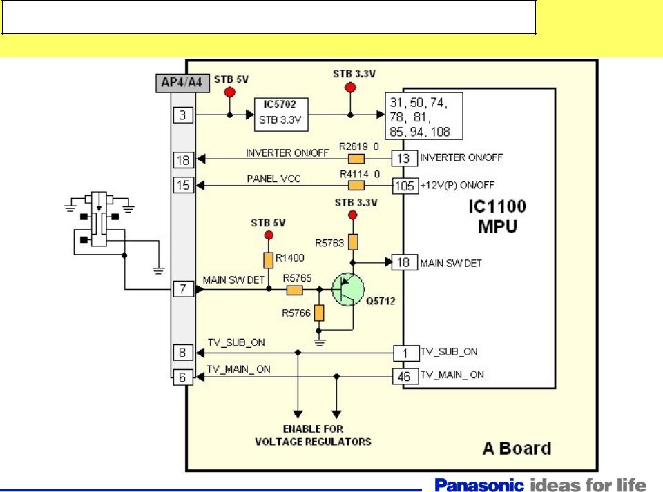
Main MPU (Power On Commands)
The STB 5V output of the P board passes through the AP board and enters the A board when the unit is plugged into the AC outlet. IC5702 of the A board converts the STB 5V to 3.3V to power the system control circuit.
Activation of the power switch causes transistor Q5712 to turn off and output STB 3.3V to pin 18 of the MPU. Upon receiving the STB 3.3V, the MPU (IC1100) outputs the TV-SUB-ON command via pin 8 of connector A4/AP4. The TVSUB_ON command is routed to the P board to provide a ground connection for relay RL802 of the power supply board. On the AP board, The TV_SUB_ON command is used to turn on a circuit (not shown in the diagram) on the A board that provides STB_5V to relay RL802. As a result , the switch of relay RL802 on the P board closes to allow the output of 105Vdc to the LCD panel. The TV_Main_ON signal issued by IC1100 appears on pin 6 of connector AP4/A4 to enable the output of the sound+12V DC/DC converter. Pin 105 of IC1100 outputs the PANEL VCC command to the AP board to turn on the 12V DC/DC converter. The 12V output is provided to the panel via the P board.
Caution: Measure the 105Vdc source between pin 1 and 3 of connector P3. Hot ground must be used.
18
Standby Operation
19

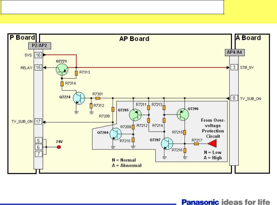
Standby Operation
When the main power switch is activated, it is sensed on the A board by the MPU IC1100. The TV_SUB_ON signal is subsequently issued in response on pin 8 of connector A4/AP4. It turns on the transistors Q7224 and Q7223 to output the “Relay voltage on pin 15 of connector AP2/P2. The TV Sub_On signal is also provided to the relay via the resistor R7208 and pin 17 of connector AP2/P2. This pulls the contacts of the AC relay on the P board. The AC input is rectified and provided to the LCD panel for conversion into 24Vdc. The 24V is then provided to the inverter circuit of the LCD panel to produce the 120Vac that powers the backlight CCFLTs. The same 24V passes through the P board and enters the AP board for conversion into other voltages.
The over-voltage protection circuitry affiliated with each of the regulators located on the AP board monitors for over-voltage conditions. It is designed to turn off the AC power by disabling the SUB_ON command that turns on the AC relay.
When an over-voltage condition is detected on the AP board, the voltage at the base of transistor Q7207 goes “high” to turn on Q7207, Q7206, Q7205, and Q7204. The TV_SUB_ON voltage at pin 17 of connector A2/AP2 is now grounded through Q7204 and the unit shuts down. To turn the unit back on, disconnect and reconnect the AC cord before pressing the power button.
20
SUB Voltages and Over-voltage Protection
The AP Board is responsible for the regulation, distribution and dissemination of all secondary voltages derived from the 24V output of the P Board. During standby operation, the 24V output of the P board biases the transistor Q7208 into operation, causing its collector to become “low”. The low at the collector of Q7208 causes the transistors Q7226, Q7227, and Q7450 to turn off. As a result, IC7205, IC7209, and IC7233 go into operation to immediately provide the Sub_5V, DT9V, BT30V, and HQ 3.3V output.
The over-voltage protection circuitry affiliated with each of the regulators monitors for excessive current and overvoltage conditions. It is designed to turn off the AC power by disabling the SUB_ON signal needed to turn on the AC
relay.
21

Main Voltages and Over-voltage Protection
When the unit is turned on, the TV_Main_On command (high) of IC1100 biases the transistor Q7212 into operation, causing its collector to go “low”. The low at the collector of Q7212 causes the transistor Q7225 to turn off. As a result, IC7215 goes into operation to provide the Sound_15V output.
When the Panel_VCC_On command is issued, transistor Q7702 turns on causing Q7701 to turn off.
Consequently, IC7212 turns on and outputs 12V. This voltage enters the A board via the connector AP4/A4. It is also provided to the LCD panel via the connector AP2/A2, the P board, and the connector P5 (not shown in the diagram).
The over-voltage protection circuitry affiliated with each of the regulators monitors for excessive current and over-voltage conditions. It is designed to turn off the AC power by disabling the SUB_ON signal needed to turn on the AC relay.
22
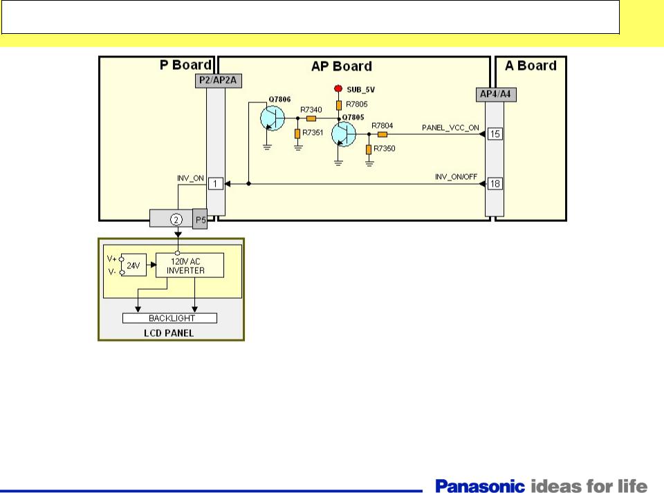
Inverter_On Command and Protection
The INV_ON/OFF command (high) of the MPU, IC1100 of the A board, passes through the AP and P boards before entering the LCD panel. On the LCD panel, it triggers the operation of the inverter to produce the 120V AC that powers the backlight CCFLTs.
To avoid catastrophic failures, when the Panel_VCC_ON pin of the MPU goes “low”, Q7805 turns off. Consequently, Q7806 turns on to disable the operation of the inverter.
23

Purposely Left Blank
Purposely left blank

Video Process Block Diagram
25

Video Process Block Diagram
The main function of the A board is to select and process one of the incoming video signals. Video inputs, component video Input, and the composite video output of the tuner are all connected to IC3001 for selection. The video output signal of the switch can be in any of the three formats: Video, Y/C, or Y, Pb, Pr. The selected output enters IC4510, the HDMI IF Receiver/Decoder IC, for A/D conversion. The comb filter inside IC4510 converts the composite video signal of the main picture to Y and C (luminance and chrominance) signals. S-Video, which is already Y/C separated, simply passes through the comb filter. The chrominance data is then applied to the Chroma Demodulator circuit to separate the color signal into Pb and Pr data. At the completion of this process, the format of the composite or S-Video signal is now the same as a digital 480i component signal. If the incoming video is in the 480p, 720P, or 1080i format, the Y, Pb, and Pr signals undergo A/D (analog to digital) conversion only. The 10 bit YUV data is provided to a video switch. The HDMI receiver section of
IC4510 converts the incoming HDMI signals to a YUV video signal. The Video interface circuit selects between the two HDMI sources and outputs the YUV signal to the switch. The output of the switch is provided to the PEAKS LITE IC, IC8001.
Digital television reception of the tuner is output in the form of a transport stream (CHODATA). The transport stream enters the DTV I/F (Interface) section of IC8001 where the video signal is extracted and converted to YUV data. The output is provided to the Video Input switch for selection. The JPEG data of the GS board enters the JPEG I/F section of
IC8001 for conversion into YUV data and output to the video switch. The video switch outputs the selected picture data to the
Video Process circuit.
The Video Process section of the IC performs all picture control operations such as brightness, contrast, color, tint, etc. The output signal is then applied to the HQ1L circuit (IC4200) for frame doubling operation. IC4200 is the circuit responsible for the Motion Picture Pro operation that reduces afterimage by 50%. On Screen Display data such as channel numbers, Digital TV closed caption, and picture adjustments are mixed with the video data. The output of IC4200 is provided to the LVDS transmitter (IC4207). The transmitter distributes signals with low-jitter, while creating little noise. It reduces power consumption and the generated noise from data transmission. Another benefit of the LVDS standard is minimal concern for cable length.
The main MCU (IC1100) controls the entire operation of the A board. It serves as the controller that monitors all operations of the TV section (not display) of the unit. When watching digital television or viewing pictures from an SD card, the video process section of IC8001 converts the digital video into analog composite video signal for output at the monitor out jack.
26

Audio Process Block Diagram
27

Audio Process Block Diagram
IC3101 of the A board handles the audio selection of most inputs. Analog audio of the tuner and audio signals from composite, component, and DVI inputs are connected to IC3101 for selection. The output of IC3101 enters IC2106 and undergoes analog to digital conversion. The serial data output is provided to the audio DSP (Digital Signal Processor).
Volume, bass, treble, and balance adjustments of the audio signal are performed by this circuit. The output is two channel
PWM data that are applied to IC2301 and IC2302 for amplification. The PWM output signals of the power amplifiers are output to the right and left channel speakers for sound reproduction. The HDMI receiver section of IC4510 converts the incoming HDMI audio into serial data. The Audio interface circuit selects between the two HDMI audio and outputs the SD (serial Data) to the switch located inside IC2106. Two outputs are provided, one for the digital audio output jack, the other for the speakers. Digital television reception of the tuner is output in the form of a transport stream that contains MPEG2 video and AC3 audio. The transport stream enters the DTV I/F section of IC8001 where the audio signal is extracted and converted to serial data. Two outputs are provided to IC2106. One output consists of the AC3 audio that will be provided to the digital audio output jack. The other output consists of left and right audio that will be used to drive the speakers. Speaker output of the DTV and HDMI audio is selected and converted to analog. The analog audio is then output to an audio amplifier (IC2011) and then applied to the audio selector (IC3101). The optical jack audio signal is also selected and processed inside IC2106. Q2303 is a muting transistor that applies a low to IC2106 when a headphone jack is connected to the unit. Q2302 applies a low to IC2106 when the mute function of the unit is active.
28

MPU SOS Inputs and Blink Codes
29

MPU SOS Inputs and Blink Codes
One Blink: One blink of the power LED indicates a problem in the inverter circuit located on the LCD panel. The inverter board is not to be repaired in the field. Therefore a replacement is required.
Three Blinks: Three blinks of the power LED indicates an over-current or over-voltage condition in one of the DC supplies of the AP board. The AP board is repairable. Therefore the use of an ohmmeter and peak-hold-voltmeter is required to determine the cause of the shutdown. An over-voltage condition is definitely a defect of the AP board. An over-current condition may be due to a short circuit located in the AP board, A board, or the LCD panel.
Five, Seven, or Eight Blinks: The A board is responsible for five, seven or eight blinks of the power LED. The MAIN +3.3V, MAIN +5V, and MAIN +9V sources are all produced on the A board. The detection input pins of the MPU, IC1100, monitor for their presence.
Four or Six Blinks: The AP board is responsible for four or six blinks of the power LED. The DTV9V, and SUB_5V
sources are produced on the AP board. The MPU IC1100 monitors for their presence when the unit is connected to AC Power. A short or open circuit on the A board may also be responsible for their absence.
Nine Blinks: Nine blinks of the power LED is due a short circuit in the audio output circuit (s) of the unit. The audio output circuit is located on the A board. Confirm the status of the speakers. If defective, perform a replacement. If ok, replace the A board.
Ten Blinks: Ten blinks of the power LED indicates a malfunction of IC4200, the frame converter. This IC resides on the A board. Therefore ten blinks of the power LED requires the replacement of the A board.
30
 Loading...