

Page 1

Nokia Customer Care
2112 (RH-57) Series Transceivers
System Module
Issue 1 07/2004 Company Confidential ©2004 Nokia Corporation
Page 2

2112 (RH-57)
System Module Nokia Customer Care
Contents Page
Introduction ..................................................................................................................................................... 3
Baseband Module ........................................................................................................................................ 3
UEM .............................................................................................................................................................. 4
BB-RF Interface Connections ...................................................................................................................6
UPP................................................................................................................................................................ 9
NOR Flash Memory and SRAM .......................................................................................................... 10
User Interface Hardware .........................................................................................................................10
LCD............................................................................................................................................................. 10
Keyboard................................................................................................................................................... 11
Power Key ................................................................................................................................................ 11
Lights......................................................................................................................................................... 11
Flashlight.................................................................................................................................................. 11
Vibra .......................................................................................................................................................... 11
Audio Hardware .........................................................................................................................................12
Earpiece .................................................................................................................................................... 12
Microphone ............................................................................................................................................. 12
MIDI Speaker........................................................................................................................................... 12
Audio Amplifier Interface.................................................................................................................... 12
Battery ..........................................................................................................................................................12
Battery Connector ................................................................................................................................. 13
Accessories Interface ................................................................................................................................14
System Connector.................................................................................................................................. 14
Charger IF................................................................................................................................................. 16
Test Interfaces ............................................................................................................................................16
Production Test Pattern ....................................................................................................................... 16
General Information About Testing ......................................................................................................19
Phone Operating Modes ...................................................................................................................... 19
RF Module ....................................................................................................................................................19
Requirements .......................................................................................................................................... 19
Antenna .................................................................................................................................................... 19
Transmitter .............................................................................................................................................. 20
Synthesizer .............................................................................................................................................. 22
Receiver ................................................................................................................................................... 24
Page 2 ©2004 Nokia Corporation Company Confidential Issue 1 07/2004
Page 3

2112 (RH-57)
Nokia Customer Care System Module
Introduction
The 2112 is available as a CDMA single-band engine (800 MHz CDMA). There are several
different operational modes, which have different states controlled by the cellular SW.
Some examples include:
• Idle State (on ACCH)
• Camping (on DCCH)
• Scanning
•Conversation
• No Service Power Save (NSPS)
In the power-off mode, only the circuits needed for power-up are supplied.
In the idle mode, circuits are powered down and only the sleep clock is running.
In the active mode, all the circuits are supplied with power, although some parts might
be in idle state part of the time.
The charge mode is effective in parallel with all previous modes. The charge mode itself
consists of two different states, the fast charge and the maintenance mode.
The Local Mode is used for alignment and testing.
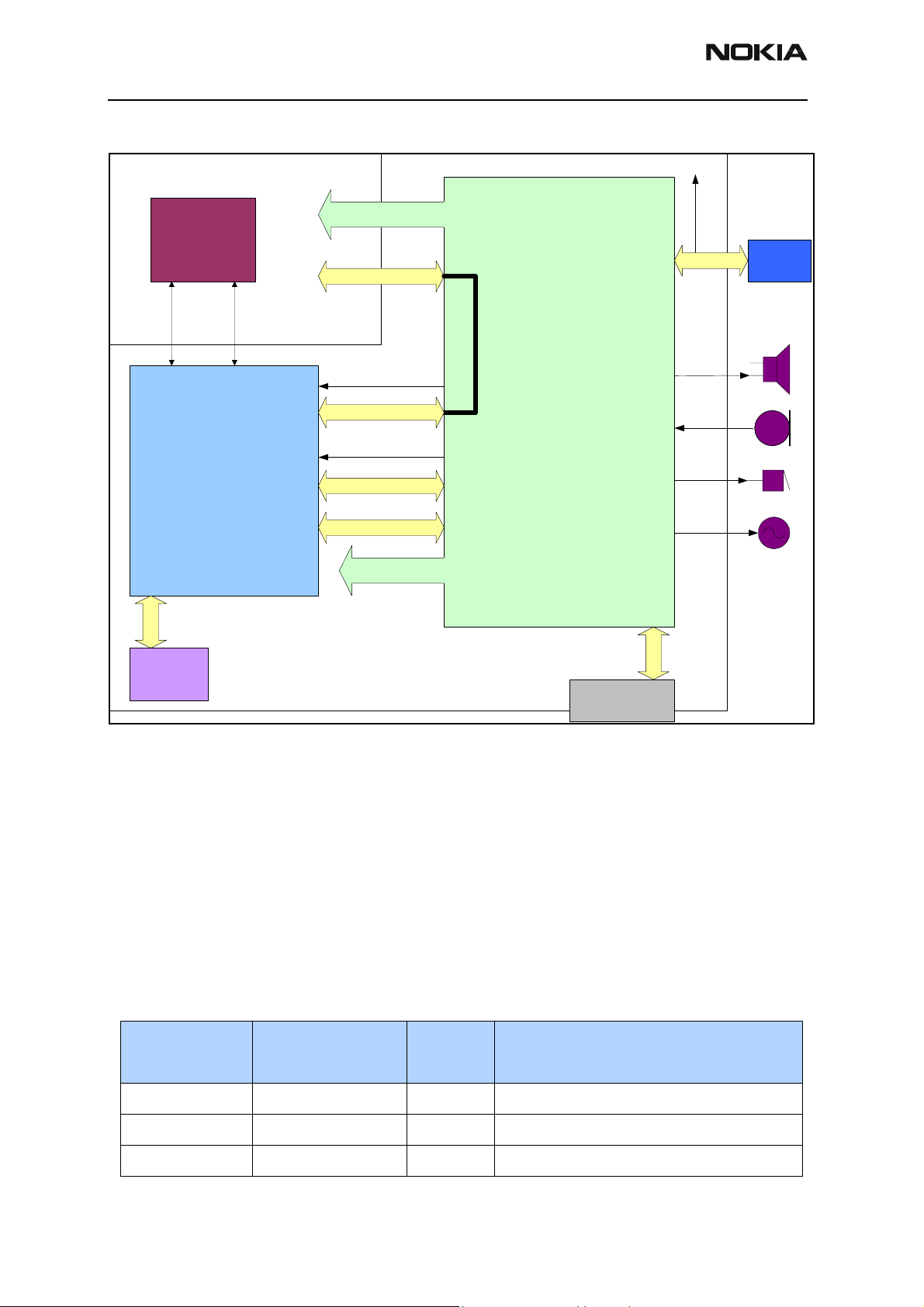
Baseband Module
The baseband module is an 800 MHz CDMA DCT4 transceiver based on the DCT4 Apollo
engine. The baseband consists of three ASICs:
• Universal Energy Management (UEM)
• Universal Phone Processor (UPP)
• 64-megabit FLASH
Issue 1 07/2004 ©2004 Nokia Corporation Company Confidential Page 3
Page 4
2112 (RH-57)
System Module Nokia Customer Care
PA Supply
RF Supplies
Apollo
BATTERY
RF RX/TX
RFIC CTRL 19.2 MHz
UEM
Ear
MIC
Buzzer
Vibra
MEMADDA
MEMCONT
FLASH
UPP
PURX
RF RX/TX
Sleep Clock 32 kHz
CBUS/DBUS
AUDIO
BB Supplies
UEM
External Audio
Charger
Connection
DCT4 System
Connector
Figure 1: Baseband module diagram
The UEM is the Universal Energy Management IC for DCT4 digital handportable phones.
In addition to energy management, it performs all the baseband mixed-signal functions.
Most UEM pins have 2kV ESD protection. Those signals that are considered to be exposed
more easily to ESD have 8kV protection inside the UEM. Such signals are all audio,
headset, BSI, Btemp, Fbus, and Mbus signals.
The baseband is powered from five different UEM regulators.
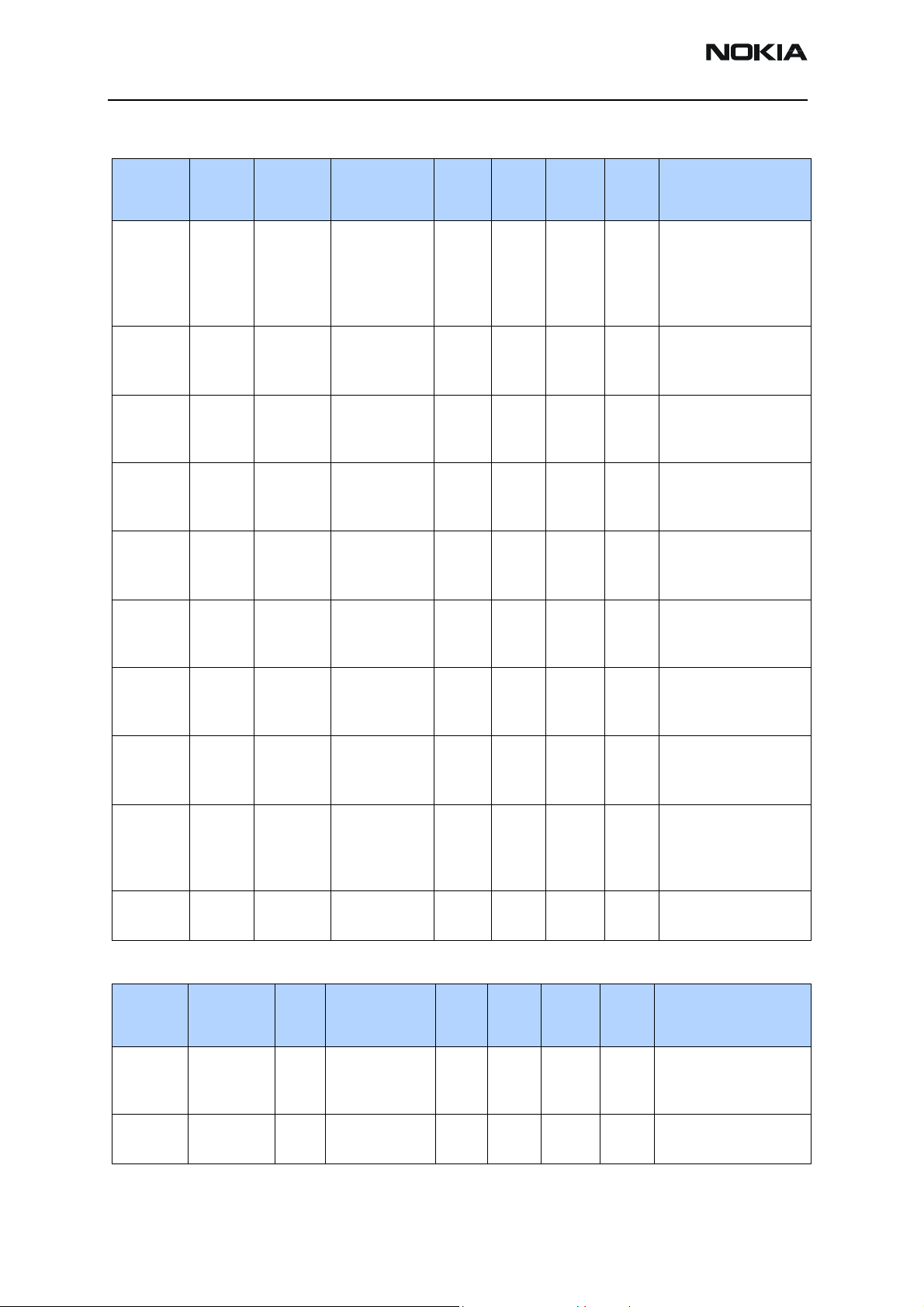
Table 1: Baseband Regulators
Regulator
Maximum
Current (mA)
Vout (V) Notes
VCORE 300 1.57/1.35 Power up default 1.57V and 1.35 in Sleep Mode.
VIO 150 1.8 Enabled always except during power-off mode
VFLASH1 70 2.78 Enabled always except during power-off mode
Page 4 ©2004 Nokia Corporation Company Confidential Issue 1 07/2004
Page 5
2112 (RH-57)
Nokia Customer Care System Module
Table 1: Baseband Regulators (Continued)
Regulator
VFLASH2 40 2.78 Enabled only when data cable is connected
VANA 80 2.78 Enabled only when the system is awake (Off
VSIM 25 3.0 Enabled only when SIM card is used
Maximum
Current (mA)
Vout (V) Notes
during sleep and power off-modes)
Table 2 includes the UEM regulators for the RF.
Table 2: RF Regulators
Regulator
VR1A 10 4.75 Enabled when cell transmitter is on
VR1B 10 4.75 Enabled when the transmitter is on
VR2 100 2.78 Enabled when the transmitter is on
VR3 20 2.78 Enabled when SleepX is high
VR4 50 2.78 Enabled when the receiver is on
Maximum
Current (mA)
Vout (V) Notes
VR5 50 2.78 Enabled when the receiver is on
VR6 50 2.78 Enabled when the transmitter is on
VR7 45 2.78 Enabled when the receiver is on
The charge pump that is used by VR1A is constructed around the UEM. The charge pump
works with the Cbus (1.2 MHz) oscillator and gives a 4.75 V regulated output voltage to
the RF.
RF Interface
In addition to the RF regulators mentioned, the UEM handles the interface between the
baseband and the RF section. It provides A/D and D/A conversion of the in-phase and
quadrature receive and transmit signal paths, and also A/D and D/A conversions of
received and transmitted audio signals to and from the UI section. The UEM supplies the
analog AFC signal to the RF section according to the UPP DSP digital control. It also
converts the PA temperature into real data for the DSP. The UPP controls the RFIC
through the 3-wire RFIC bus. In addition, the UPP provides a PDM regulator for RF
interface (RX/TX AGC control).
Charging Control
The CHACON block of the UEM controls charging. Needed functions for charging controls
are the PWM-controlled battery charging switch, charger-monitoring circuitry, battery
voltage monitoring circuitry, and RTC supply circuitry for backup battery charging. In
Issue 1 07/2004 ©2004 Nokia Corporation Company Confidential Page 5
Page 6
2112 (RH-57)
System Module Nokia Customer Care
addition, external components are needed for EMC protection of the charger input to the
baseband module. The DCT4 baseband is designed to electrically support both DCT3 and
DCT4 chargers.
Digital Interface
Data transmission between the UEM and the UPP is implemented using two serial
connections: DBUS (9.6 MHz) for the DSP and CBUS (1.2 MHz in CDMA) for the MCU. The
UEM is a dual-voltage circuit. The digital parts run from 1.8 V and the analog parts run
from 2.78 V. The Vbat (3.6 V) voltage regulator inputs are also used.
Audio Codec
The baseband supports two external microphone inputs and one external earphone
output. The inputs can be taken from an internal microphone, from a headset
microphone, or from an external microphone signal source through a headset connector.
The output for the internal earpiece is a dual-ended output, and the differential output is
capable of driving 4Vpp to the earpiece with a 60 dB minimum signal to total distortion
ratio. Input and output signal source selection and gain control is performed inside the
UEM ASIC according to control messages from the UPP. Both the buzzer and external
vibra alert control signals are generated by the UEM with separate PWM outputs.
MIDI
The MIDI audio signal generated by the DSP and UEM audio CoDec is routed to the XEAR
output of the UEM. An audio amplifier (LM4890) is used to boost enough power for the
speaker.
UI Drivers
The vibra, display LED, and keyboard LEDs are driven by open collector output drivers
inside the UEM. These drivers can generate PWM square wave signals to these devices.
AD Converters
There is an 11-channel analog-to-digital converter in the UEM. The AD converters are
calibrated in the production line.
BB-RF Interface Connections
All the signal descriptions and properties in the following tables are valid only for active
signals.
Signal
Name
From To Parameter Min Type Max Unit Function
Table 3: PDM Interface
RX_IF_AGC UPP
GenIO 9
Yoda Voltage Min
Max
-------------Clk Rate
(1)
0.0
1.75
------
1.8
----
9.6
0.1
1.86
-----
19.2
V
----MHz
Controls gain of
VGA r in receiver
Page 6 ©2004 Nokia Corporation Company Confidential Issue 1 07/2004
Page 7
2112 (RH-57)
Nokia Customer Care System Module
Table 3: PDM Interface (Continued)
Signal
Name
TX_IF_AGC UPP
TX_RF_AGC UPP
Signal
Name
TX_Gate UPP
From To Parameter Min Type Max Unit Function
GenIO 7
GenIO 26
From To Parameter
Gen IO 8
pullup
Jedi Voltage Min
Max
-------------Clk Rate
Jedi Voltage Min
Max
-------------Clk Rate
Jedi and
PA Gating
Transistors
(1)
(3)
Table 4: General I/O Interface
“0” Transmitter Off
“1” Transmitter On
Timing Accuracy
0.0
1.75
-----
0.0
1.75
------
0.1
1.8
-----
9.6
1.8
-----
9.6
1.86
-----
19.2
0.1
1.86
------
19.2
Input
Characteristics
1.38 1.88 V
0 0.4 V
4 chips, and can be
up to a total of
255 chips
V
----MHz
V
----MHz
Controls gain of
VGA in IF VGA
Controls gain of
TX driver
Function
Punctures the PAs and
the Jedi ASIC
Digital Into RF
D0 UPP
Gen IO 10
D1 UPP
Gen IO 13
D2 UPP
Gen IO 12
Signal
Name
19.2M_UPP Yoda UPP Frequency
AFC UEM VCT
From To Parameter Min Type Max Unit Function
PMIC Voltage Min
PMIC Voltage Min
PMIC Voltage Min
-------------Signal amplitude
Voltage Min
CXO
Max
--------------Settling time
0.4V max
Max
Max
Max
Table 5: VCTCXO Interface
-----
0.5
0.0
2.4
------ -----
(4)
1.72V-1.86V
0.4V max
1.72V-1.86V
0.4V max
1.72V-1.86V
19.2
-----
1.0
--
-----
1.5
0.1
2.55
-----
0.2
Enable PMIC
Set PMIC output voltage
Set PMIC output voltage
MHz
----Vpp
V
----ms
High stability
clock signal for
logic circuits, AC
coupled
sinewave.
Automatic
frequency
control signal for
VCTCXO
Digital Into RF
Issue 1 07/2004 ©2004 Nokia Corporation Company Confidential Page 7
Page 8
2112 (RH-57)
System Module Nokia Customer Care
Table 6: Regulated Supplies from UEM to RF
Signal
Name
VBAT Battery PA &
VR1A UEM PA Vref Voltage
VR2 UEM Jedi Voltage
VR3 UEM VCTCXO,
VR4 UEM Alfred Voltage
VR5 UEM Jedi Voltage
From To Parameter Min Type Max Unit Function
Voltage
UEM,
external
driver
amps
Yoda
-------------
Current
-------------
Current
-------------
Current
Voltage
-------------
Current
-------------
Current
-------------
Current
3.2
----0
4.6
----0
2.70
-----
2.70
-----
2.70
-----
2.70
-----
3.5
-----
-
4.75
----4
2.78
-----
2.78
-----
2.78
-----
2.78
-----
5.1
----2A
peak
4.9
----5
2.86
----100
2.8
----20
V
-----
V
----mA
V
----mA
V
----mA
V
----mA
V
----mA
Battery supply. Lower
limit is to guarantee
regulator PSRR
Charge pump + linear regulator.
Linear regulator
Low noise linear regulator for VCTCXO
Low lq linear
regulator
Low lq linear
regulator
VR6 UEM Yoda Voltage
-------------
Current
VR7 UEM Jedi Voltage
-------------
Current
VIO UEM Jedi,
Yoda
Vref_rf01 UEM Yoda Voltage 1.334 1.35 1.366 V Voltage refer for Yoda
Signal
Name
PA_TEMP Thermistor UEM Input voltage
PWROUT Jedi UEM Input voltage
From To Parameter Min Type Max Unit Function
Voltage 1.70 1.8 1.88
Table 7: Slow A/D Converters
range
range
2.70
------
2.70
------
0 2.78 V PA temperature sen-
0 2.78 V Buffered output of TX
2.78
-----
2.78
-----
-----50
V
----mA
V
----mA
V
----mA
Low lq linear
regulator
Low noise linear regulator for
synthesizer
Supply for RF-BB digital signal interface
and some digital
parts of RF
I/or de-modulator
sor output voltage
Analog Out of RF
output detector
Page 8 ©2004 Nokia Corporation Company Confidential Issue 1 07/2004
Page 9

2112 (RH-57)
Nokia Customer Care System Module
Table 8: RF-BB Analog Signals
Signal
Name
RX_IP_RF
RX_IN_RF
RX_QP_RF
RX_QN_RF
TX_IP_RF
TX_IN_RF
TX_QP_RF
TX_QN_RF
Signal
Name
RF_BUS_CLK
RF_BUS_DATA
RF_BUS_EN1X
From To Parameter Min Type Max Unit Function
Yoda UEM Differential volt-
age swing (static)
--------------DC level
--------------Input Bandwidth
UEM Jedi Differential volt-
age swing (static)
----------------DC level
-----------------
-3 dB Bandwidth
Table 9: RFIC Control
0.3
-----
1.3
-----
0.4
-----
1.65
----650
0.5
-----
1.35
-----
0.8
----
1.7
----
1.0
-----
1.4
----615
1.2
----
1.75
----1950
Vpp
---V
---kHz
Vpp
---V
---kHz
Differential in-phase
and quadrature RX
baseband signal
Analog Out of RF
Differential quadrature phase TX baseband signal for RF
modulator
Analog into RF
From To Parameter Min Type Max Unit Function
UPP Jedi,
Yoda
High-level input
voltage, V
Low-level input
voltage, V
IH
IL
1.72
1.8
1.86
0.4
V
V
Serial Clock =
Digital Into RF
Bidirectional Serial
Date = Digital I/O
UPP
High-level out-
put voltage, V
Low-level out-
put voltage, V
Clock
OH
OL
1.72
1.8
9.6
1.86
0.4
V
V
MHz
Latch enable for
Jedi and Yoda =
Digital Into RF
The 2112 uses a UPP8Mv3.5 ASIC with an 8Mbit RAM size. The UPP ASIC is designed to
operate in a DCT4 engine, and is designed as part of the DCT4 common baseband task
force. The DCT4 processor architecture consists of both DSP and MCU processors.
The UPP is internally partitioned into two main parts: the Brain and the Body.
The Brain consists of the processor and memory system (i.e., processor cores, mega-cells,
internal memories, peripherals, and the external memory interface). The following blocks
are included:
• DSP Subsystem (DSPSS)
• MCU Subsystem (MCUSS)
• Emulation control EMUCtl
Issue 1 07/2004 ©2004 Nokia Corporation Company Confidential Page 9
Page 10

2112 (RH-57)
System Module Nokia Customer Care
• Program/data RAM PDRAM
• Brain Peripherals–subsystem (BrainPer)
The Body consists of the NMP custom cellular logic functions. These contain all
interfaces and functions needed for interfacing with other DCT4 baseband and RF parts.
The following sub-blocks are included:
•MFI
•SCU
•CTSI
•RxModem
• AccIF
•UIF
•Coder
• GPRSCip
•BodyIF
• SIMIF
•PUP
• CDMA (Corona)
NOR Flash Memory and SRAM
This device is a 64Mbit, mixed burst, multi-bank Flash and 8Mbit Muxed fCMOS SRAM
combined in a multi-chip package memory.
The 64Mbit Flash memory is organized as 8M x 16 bit, and the 8Mbit SRAM is organized
as 512K x 16 bit. The Flash memory architecture is designed to divide its memory arrays
into 263 blocks, which provides highly flexible erase and program capability. This device
is capable of reading data from one bank while programming or erasing in the other
banks with multi-bank organization.
The Flash memory performs a program operation in units of 16 bits (Word) and erases in
units of a block. Single or multiple blocks can be erased. The block erase operation is
completed for typically 0.7 sec.
The 8Mbit Muxed fCMOS SRAM supports low data retention voltage for the battery
backup operation with a low data retention current.
User Interface Hardware
LCD
The 2112 uses a black and white, 96 X 65 display. The LCD is controlled by UI SW and
control signals.
Page 10 ©2004 Nokia Corporation Company Confidential Issue 1 07/2004
Page 11
2112 (RH-57)
Nokia Customer Care System Module
Keyboard
The keyboard design is a 4-way scroll with navigation keys, two soft keys, and 12 number
keys. The power key is located on top.
Power Key
All signals for the keyboard come from the UPP ASIC, except the power key signal, which
is connected directly to the UEM. Pressing the power key creates an interrupt and
connects the PWONX to the GND.
Lights
The 2112 has six white LEDs for keyboard lighting purposes. The LEDs for the display are
integrated into the display module.
Display lighting and keyboard lights are controlled by the UEM Klight signal (8-bit
register DriverPWMR, bits 7...4). The Klight output is a Pulse Width Modulation (PWM)
signal, which is used to control the average current going through the LEDs. A step-up
converter and a constant current source are used to ensure that the LEDs provide
uniform intensity.
Flashlight
The flashlight feature is driven by the White LED Driver and controlled by the UEM. The
circuit for the flashlight is driven by TK11851TL. In this situation, the driver is used as a
boost DC/DC. Vout is set using three precision resistors in R300, R316, and 317.
Vout = Vfb * (1+ (R316+R317)/ R300). The TK11851L is an active-high enable device,
whose enable signal is tied to Klight/Dlight signals from the UEM. When Klight goes high
it turns on the TK11851TL driver and the V301 transistor, which allows a path to GND.
Vibra
The vibra is located on the bottom of the D-cover and is connected by spring connectors
on the PWB.
The vibra is controlled by a VIBRA PWM signal from the UEM. This signal allows control
of both frequency and pulse width of the signal. Pulse width is used to control the
current when the battery voltage changes. Frequency control searches for optimum
frequency to ensure silent and efficient vibrating.
Table 10: Vibra Parameters
Parameter Requirement Unit
Rated DC voltage 1.3 V
Rated speed 9500 ± 3000 rpm
Rated current 115 ± 20 mA
Starting current 150 ± 20 mA
Armature resistant 8.6 ohm
Issue 1 07/2004 ©2004 Nokia Corporation Company Confidential Page 11
Page 12

2112 (RH-57)
System Module Nokia Customer Care
Table 10: Vibra Parameters (Continued)
Parameter Requirement Unit
Rated DC voltage available 1.2 to 1.7 V
Starting DC voltage min 1.2 V
Audio Hardware
Earpiece
The 2112 uses the 13 mm speaker capsule that is used in DCT3. The speaker is dynamic,
very sensitive, and capable of producing relatively high sound pressure at low
frequencies. The speaker capsule and surrounding mechanics comprise the earpiece.
Microphone
The microphone is an electric microphone with an omnidirectional polar pattern.
It consists of an electrically polarized membrane and a metal electrode, both of which
form a capacitor. Air pressure changes (i.e., sound) move the membrane, which causes
voltage changes across the capacitor. Since the capacitance is typically 2 pF, a FET buffer
is needed inside the microphone capsule for the signal generated by the capacitor. The
microphone needs bias voltage as a result of the FET.
MIDI Speaker
Musical Instrument Digital Interface (MIDI) defines the data interchange format. By
implementing a MIDI engine, enriched sound effects are achieved, which include ring
tones, UI event sounds, and music for games and entertainment.
The MIDI data stream is a unidirectional, asynchronous bit stream at maximum
31.25 kbits/sec with 10 bits transmitted per byte (a start bit, 8 data bits, and one stop
bit).
MIDI data includes two categories of signals: MIDI tones and Alerting Tones. Both are
generated from the DSP and sent to the MIDI speaker.
Audio Amplifier Interface
Because the audio output from the UEM is not strong enough to produce enough power
for the speaker, an audio amplifier is required. The MIDI audio signal generated by the
DSP and UEM audio CoDec is routed to the XEAR output of the UEM. An audio amplifier
is used to boost enough power for the speaker. GENIO (28) is used to enable/disable the
audio amplifier as needed.
Battery
An 850 mAh Li-ion battery (BL-5C) is standard in the 2112. The battery block contains
BSI resistors for battery identification. The BSI fixed resistor value indicates the
chemistry and default capacity of a battery. This resistor is connected to the BSI pin of
Page 12 ©2004 Nokia Corporation Company Confidential Issue 1 07/2004
Page 13

2112 (RH-57)
Nokia Customer Care System Module
the battery connector. The phone has pull-up resistors (R202) for these lines so that they
can be read by A/D inputs in the phone. There also are spark caps in the BSI line to
prevent ESD. The battery also has internal protection for overvoltage and overcurrent.
Figure 2: Battery interface
Battery Connector
The 2112 uses a spring-type battery connector. This ensures a more reliable connection
between the battery and PWB
Figure 3: Battery pack pin order
Table 11 shows the properties for the battery pack pins.
Table 11: Battery Pin Properties
Signal
Name
1 VBAT (+) (batt.) VBAT I/O
2 BSI BSI (batt.) UEM Out
3 GND GND GND
Connected
From - To
Batt I/O
Signal Properties A/D
Levels Freq/Timing
Description
Issue 1 07/2004 ©2004 Nokia Corporation Company Confidential Page 13
Page 14

2112 (RH-57)
System Module Nokia Customer Care
Accessories Interface
System Connector
The 2112 uses Tomahawk accessories via the Tomahawk connector. The Tomahawk
bottom connector consists of a charging plug socket and a Tomahawk System connector
(see figures that follow). The minimum configuration for the Tomahawk interface
includes charging, mono audio, power out, ACI, and Fbus. The USB and stereo audio out
are optional.
The Tomahawk system connector includes:
• Charging
Pads for 2 -wire charging in cradles
•Audio
• 2 -wire fully differential output audio
• 2-wire differential mic input
•Power out
• 2.78V 70 mA output to accessories
• Detection/controlling
•ACI
• Point to point bi-directional data line
•Fbus
• Standard Fbus
• AT command mode (Nokia Serial Bus)
• Phone message mode
• Fast Fbus, fast data bus to add on modules
Page 14 ©2004 Nokia Corporation Company Confidential Issue 1 07/2004
Page 15

2112 (RH-57)
Nokia Customer Care System Module
Metal shield
Plastic housing
9.50
Figure 4: Tomahawk system connector
Contacts (14 pieces)
Locking holes for
accessories (2 pieces)
6.50
5.70
6.55
5.40
1.00
2.70
21.20
PWB
0.30
Metal
shielding
ACI
Vout
Charge GND
Shielding GND
USB Vbus
USB D+ / Fbus RX
USB D- / Fbus TX
XMIC P
XMIC N
DATA GND
HSEAR P
HSEAR N
HSEAR R P
HSEAR R N
Figure 5: Mechanical dimensions and signals of Tomahawk bottom connectors
An accessory is detected by the ACI-line. All accessories will generate interrupt while
inserted or removed from the phone’s Tomahawk system connector. Insertion of an
accessory will generate HEADINT interrupt by pulling the ACI line down. Vout is enabled
by the UPP. The MBUS line is connected to the HEADINT line. If the HEADINT interrupt
from low to high transition occurs within 20msec, either a more advanced accessory is
connected or a basic headset is connected.
3.50
Shielding GND
Issue 1 07/2004 ©2004 Nokia Corporation Company Confidential Page 15
Page 16

2112 (RH-57)
System Module Nokia Customer Care
Charger IF
The charger connection is implemented through the bottom connector. The DCT-4
bottom connector supports charging with both plug chargers and desktop stand
chargers.
There are three signals for charging. The charger GND pin is used for both desktop and
for plug chargers as well as the charger voltage. The PWM control line, which is needed
for 3-wire chargers, is connected directly to the GND in the PWB so the 2112 engine
does not provide any PWM control to chargers. Charge controlling is done inside the
UEM by switching the UEM internal charger switch on/off.
The fuse (F100) protects from high currents (e.g., when broken or pirate chargers are
used). The L100 protects the engine from RF noises that may occur in a charging cable.
V100 protects the UEM ASIC from reverse-polarity charging and from high-charging
voltage. The C106 is also used for ESD and EMC protection.
Test Interfaces
Production Test Pattern
The interface for 2112 production testing is a 5-pin pad layout in the BB area (see
Figure 6). A production tester connects to these pads using spring connectors. The
interface includes MBUS, USRX, FBUSTX, VPP, and GND signals. The pad size is 1.7mm.
The same pads also are used for AS test equipment, such as a module jig and a service
cable.
Figure 6: 5-pin layout in BB area
Page 16 ©2004 Nokia Corporation Company Confidential Issue 1 07/2004
Page 17

2112 (RH-57)
Nokia Customer Care System Module
Figure 7: Test points (bottom)
Issue 1 07/2004 ©2004 Nokia Corporation Company Confidential Page 17
Page 18

2112 (RH-57)
System Module Nokia Customer Care
Figure 8: Test points (top)
Page 18 ©2004 Nokia Corporation Company Confidential Issue 1 07/2004
Page 19

2112 (RH-57)
Nokia Customer Care System Module
General Information About Testing
Phone Operating Modes
The phone has three different modes for test/repair. Modes can be selected with suitable
resistors connected to BSI lines as follows:
Table 12: Test/Repair Modes
Mode BSI Resistor Notes
Normal 75k
Local 3.3k
Test 6.8k Recommended with baseband testing. Similar to
Local mode, but making a phone call is possible.
The MCU software enters automatically to Local or Test mode at start-up if
corresponding resistors are connected.
Note: The baseband does not wake up automatically when the battery voltage is connected (Normal
Mode).
RF Module
Requirements
The 2112 supports CDMA 800 MHz as described in the following documents:
• IS2000-2-A Physical Layer Standard for CDMA2000 Spread Spectrum Systems
• IS-98D (Draft 4) Recommended Minimum Performance Standard for Spread
Antenna
An internal antenna is used.
Spectrum Mobile Stations
Issue 1 07/2004 ©2004 Nokia Corporation Company Confidential Page 19
Page 20

2112 (RH-57)
System Module Nokia Customer Care
Transmitter
Antenna
Antenna
Antenna
Antenna
I
I
I
From
From
From
From
Baseband
Baseband
Baseband
Baseband
Q
Q
Q
BB I LPF
457.2MHz
VHF LO
VHF LO
VHF LO
VHF LO
÷2/÷4
÷2/÷4
÷2/÷4
÷2/÷4
IQ Modulator
0º
0º
0º
90º
90º
90º
90º
IF VGA
(IF AGC PDM)
UHF LO
UHF LO
UHF LO
0º
0º
0º
0º0º
90º
90º
90º
1052.61-107757MHz
Figure 9: RF transmitter block diagram
Upconverter
0º
0º
0º
0º
0º
0º
0º0º
90º
90º
90º
90º
90º
90º
90º
90º
RF VGA
(RF AGC PDM)
TP1
Bandpass
Tx SAW
To Baseband
To Baseband
To Baseband
PWR Amplifier
TP2 TP3
Power
Power
Power
Power
Detector
Detector
Detector
Detector
Isolator
Isolator
Isolator
TP4
Cell RX
Cell RX
Cell RX
Cell RX
Duplexer
Duplexer
Duplexer
Duplexer
Page 20 ©2004 Nokia Corporation Company Confidential Issue 1 07/2004
Page 21

2112 (RH-57)
Nokia Customer Care System Module
The transmit chain up to the RF driver stage is integrated into one transmit-integrated
circuit (Jedi) with external power amplifiers (PA). The channel spacing is 30 kHz.
All data transmitted on the channel is convolutionally encoded and block-interleaved.
Modulation is 64-ary orthogonal (RC1 and RC2) and the direct sequence is spread by a
quadrature pair of PN sequences at a fixed chip rate. The data is filtered, O-QPSK
modulated, and up-converted to the appropriate transmission frequency. RC3 and RC4
use HPSK modulation at data rates up to 153.6 kBPS (RC3) and 115.2 kBPS (RC4).
The baseband I/Q signals are converted to an IF frequency in the I/Q modulator by
quadrature mixing. The modulated IF signals go through a variable gain amplifier
(IF AGC) and then are routed to the Cell Tx path. The path consists of an upconverter and
a variable gain RF amplifier. The IF signal is converted up to RF with a differential output
upconverter and then fed to the RF amplifier. The RF amplifier has variable gain
capability (RF AGC) with up to 40 dB of dynamic gain control.
The output of Jedi’s Cell RF amplifier is connected to an RF filter to reject TX noise in the
RX band. The output of the RF filter goes to the PA, to an isolator, and finally to the
antenna.
Issue 1 07/2004 ©2004 Nokia Corporation Company Confidential Page 21
Page 22

2112 (RH-57)
System Module Nokia Customer Care
Synthesizer
Figure 10 illustrates the synthesizers and how they interconnect in the system.
CELL:457.2MHz
CELL:457.2MHz
JEDI
JEDI
367.2MHz
367.2MHz
VHF
VHF
counter
counter
Yoda
Yoda
19.2MHz
19.2MHz
VCTCXO
VCTCXO
19.2MHz to
19.2MHz to
UPP
UPP
VHF
VHF
counter
counter
UHF
UHF
counter
counter
Figure 10: Synthesizer system block diagram
CELLl Band UHF VCO
CELLl Band UHF VCO
Page 22 ©2004 Nokia Corporation Company Confidential Issue 1 07/2004
Page 23

2112 (RH-57)
Nokia Customer Care System Module
1st TX VHF LO Synthesizer (Jedi)
The TX VHF synthesizer is integrated within the Jedi RFIC and generates the LO signals
for the IQ-modulator in Jedi. The synthesizer has an internal VCO with an external
resonator. The VCO operates at two times the Cell IF frequencies. A band-switch signal
(VCO_Band) is used to shift the center frequency of the external resonator.
The synthesizer is a dual-modulus prescaler and utilizes a phase detector with a charge
pump that sinks or sources currents, depending on the phase difference between the
detector input signals. The width of the pulses depends on the phase difference between
the signals at input of the phase detector. The main divider, auxiliary divider, and
reference divider are programmable through the serial interface to Jedi.
The TX VHF synthesizer generates 457.2MHz, and the comparison frequency is 30 kHz.
2nd RX VHF LO Synthesizer (Yoda)
The RX VHF synthesizer is integrated within the Yoda RFIC and generates the LO signals
for the IQ demodulator in Yoda. The synthesizer has an internal VCO with an external
resonator. The VCO operates at two times the common 183.6 MHz (367.2 MHz) RX IF
frequency.
The synthesizer is a dual-modulus prescaler and utilizes a phase detector with a charge
pump that signals or sources currents, depending upon the phase difference between the
detector input signals. The width of the pulses depends on the phase difference between
the signals at input of the phase detector. The main divider, auxiliary divider, and
reference divider are programmable through the serial interface to Yoda.
The RX VHF synthesizer generates 367.2 MHz.
VCTCXO - System Reference Oscillator
The VCTCXO provides the frequency reference for all the synthesizers. It is a voltagecontrolled, temperature-compensated, 19.2MHz crystal oscillator that can be pulled over
a small range of its output frequency. This allows for an AFC function to be implemented
for any frequency accuracy requirements. This is done by DSP processing of received I/Q
signals.
Closed loop AFC operation allows very close frequency tracking of the base station to be
done in CDMA mode. This enables the unit to track out aging effects and gives the
required center frequency accuracy in Cell band.
The most practical way of clock distribution is driving the two chips (Yoda and Jedi)
directly from the VCTCXO. An internal buffer is used to drive the UPP in order to isolate
the UPP’s digital noise from the VCTCXO, which prevents contamination of the 19.2 MHz
reference onto the PLL chips of the system. Because the VCTCXO output is a sinewave,
clock distribution does not cause any clock signal integrity problems, even for relatively
long traces (which might occur in the case of a digital square waveform with fast
transition times). The VCTCXO output is AC, coupled to Yoda, Jedi, and the digital ASICs.
Issue 1 07/2004 ©2004 Nokia Corporation Company Confidential Page 23
Page 24

2112 (RH-57)
÷
System Module Nokia Customer Care
Receiver
LNA SW Control
I/Q Down
Converter
CDMA
BB Filter
TX
Antenna
Duplexer
LNA
CELL
SAW
Loop Filter
RFA
UHF VCO
1052.61-1077.57
UHF Synthsizer
JEDI
IFA
IF SAW
VCTCXO
VGA
CDMA
BB Filters
2
BB AMP
To BB
BB AMP
VHF PLL
367.2 MHz
Bias and Control
Reference Clock
To Base-Band
AFC
Figure 11: Receiver block diagram
Page 24 ©2004 Nokia Corporation Company Confidential Issue 1 07/2004
Page 25

2112 (RH-57)
Nokia Customer Care System Module
The receiver is a dual conversion I/Q receiver with a first IF of 183.6 MHz. The front-end
RFIC (Alfred) contains a low noise amplifier (LNA), a radio frequency amplifier (RFA), a
down-converter, an intermediate frequency amplifier (IFA), and a local oscillator
amplifier (LOA). Between the LNA and the RFA is a bandpass filter, which rejects out-ofband spurious and acts as image rejection. The IF filter is between the Alfred IC and the
Yoda IC. The purpose of this filter is to guarantee rejection in adjacent and alternate
channels.
The RX IF ASIC Yoda is used to convert the IF down to baseband I and Q. The ASIC
contains a VGA section, an IQ demodulator, and baseband filters (BBFIL) for CDMA. Fix
gain baseband amplifier (BBAMP), and RX VHF PLL. The I/Q BB signals are output to the
UEM chip for analog-to-digital conversion and further signal processing.
Issue 1 07/2004 ©2004 Nokia Corporation Company Confidential Page 25
Page 26

2112 (RH-57)
System Module Nokia Customer Care
This page intentionally left blank.
Page 26 ©2004 Nokia Corporation Company Confidential Issue 1 07/2004
 Loading...