

Page 1

Nokia Customer Care
2112 (RH-57) Series Transceivers
Troubleshooting — BB
Issue 1 07/2004 Company Confidential ©2004 Nokia Corporation
Page 2

2112 (RH-57)
Troubleshooting — BB Nokia Customer Care
Contents Page
Baseband Troubleshooting........................................................................................................................... 4
2112 Baseband Module Overview .......................................................................................................... 4
Baseband and RF Architecture ................................................................................................................5
Power Up and Reset ....................................................................................................................................6
Power Up - Power Key............................................................................................................................. 8
Power Up - Charger ................................................................................................................................. 8
Power Up - RTC Alarm............................................................................................................................. 9
Power Off .......................................................................................................................................................9
Power Consumption and Operation Modes ......................................................................................... 9
Power Distribution ....................................................................................................................................10
Clock Distribution ......................................................................................................................................12
RFClk (19.2 MHz Analog)..................................................................................................................... 12
RFConvClk (19.2 MHz digital)............................................................................................................ 14
CBUS Clk Interface ................................................................................................................................ 15
DBUS Clk Interface ................................................................................................................................ 15
SleepCLK (Digital) .................................................................................................................................. 16
SleepCLK (Analog).................................................................................................................................. 16
Flash Programming ...................................................................................................................................17
Connections to Baseband.................................................................................................................... 17
Baseband Power Up .............................................................................................................................. 17
Flash Programming Indication ........................................................................................................... 17
Flashing..................................................................................................................................................... 18
Flash Programming Error Codes ........................................................................................................ 20
Charging Operation ...................................................................................................................................21
Battery ...................................................................................................................................................... 21
Charging Circuitry ................................................................................................................................. 21
Charger Detection.................................................................................................................................. 22
Charge Control ....................................................................................................................................... 23
Audio .............................................................................................................................................................23
Display and Keyboard ...............................................................................................................................23
Flashlight.................................................................................................................................................. 24
Accessories ..................................................................................................................................................24
Charging ................................................................................................................................................... 25
Tomahawk Headset Detection ........................................................................................................... 26
FBus Detection........................................................................................................................................ 27
Accessory Detection Through ACI..................................................................................................... 28
SIM CAR .......................................................................................................................................................29
Test Points ...................................................................................................................................................31
Troubleshooting .........................................................................................................................................33
Top Troubleshooting Map ........................................................................................................................34
Phone is Totally Dead ........................................................................................................................... 36
Flash Programming Does Not Work ................................................................................................. 37
Power Does Not Stay on or the Phone is Jammed ....................................................................... 39
Charger ..................................................................................................................................................... 41
Audio Faults............................................................................................................................................. 42
Display Faults.......................................................................................................................................... 46
Keypad Faults.......................................................................................................................................... 48
Page 2 ©2004 Nokia Corporation Company Confidential Issue 1 07/2004
Page 3

2112 (RH-57)
Nokia Customer Care Troubleshooting — BB
Flashlight.................................................................................................................................................. 50
Issue 1 07/2004 ©2004 Nokia Corporation Company Confidential Page 3
Page 4

2112 (RH-57)
Troubleshooting — BB Nokia Customer Care
Baseband Troubleshooting
2112 Baseband Module Overview
The baseband module of the 2112 transceiver is a CDMA single-band engine. The
baseband architecture is based on the DCT4 Apollo engine.
The 2112 cellular baseband consists of three ASICs: Universal Energy Management
(UEM), Universal Phone Processor (UPP), and a 64 megabit FLASH.
The baseband architecture supports a power-saving function called sleep mode. Sleep
mode shuts off the VCTCXO, which is used as the system clock source for both the RF and
the baseband. During sleep mode, the system runs from a 32 kHz crystal and all the RF
regulators (VR1A, VR1B, VR2, … VR7) are off. The sleep time is determined by network
parameters. Sleep mode is entered when both the MCU and the DSP are in standby mode
and the normal VCTCXO clock is switched off. The phone is waken up by a timer running
from this 32 kHz clock supply. The period of the sleep/wake up cycle (slotted cycle) is
1.28N seconds, where N= 0, 1, 2, depending on the slot cycle index.
2112 supports standard Nokia 2-wire and 3-wire chargers (ACP-x and LCH-x). However,
the 3-wire chargers are treated as 2-wire chargers. The PWM control signal for
controlling the 3-wire charger is ignored. UEM ASIC and EM SW control charging.
BL-5C Li-ion battery is used as main power source and has nominal capacity of 850 mAh.
Page 4 ©2004 Nokia Corporation Company Confidential Issue 1 07/2004
Page 5
2112 (RH-57)
Nokia Customer Care Troubleshooting — BB
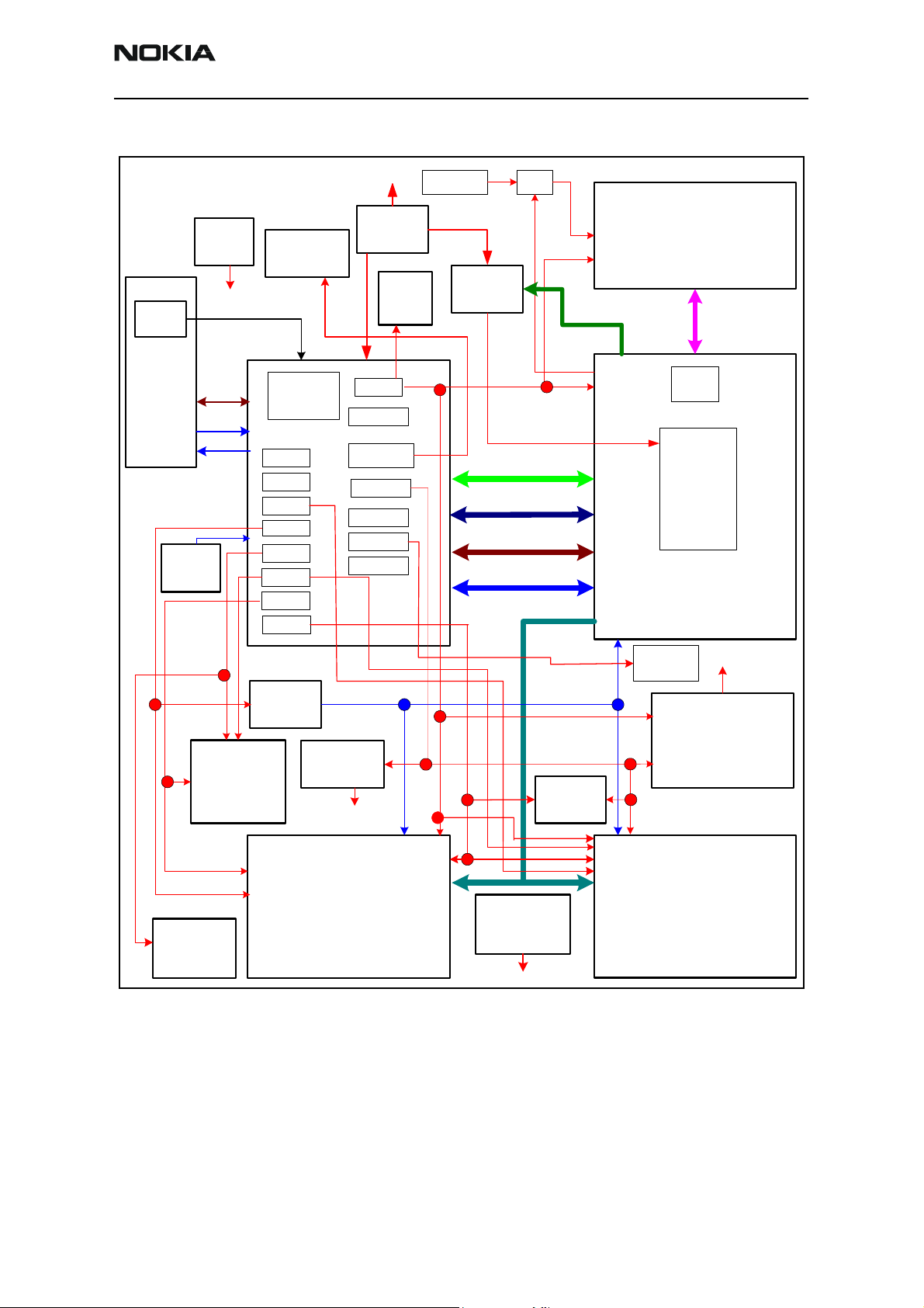
Baseband and RF Architecture
Charger
Bottom
Conn.
Sleep Clk
32 KHz
Audio
MBus
FBusRx
FBusT
x
SIM Reader
UEM
VR1A
VR1B
VR2
VR3
VR4
VR5
VR6
VR7
VBatt
Battery
JTAG
VIO
VANA
V SIM
Vflash1
Vflash2
Dlight
Klight
DC/DC
VPPPRODTP
CBus
u
B
D
MBus
FBus
GenIO
Control
s
Flash
C
ExtBus
UPP
Core
Alfred
Front
End
VCTCXO
19.2 MHz
RF
System
Connector
V Bat
Bus
UHF
SYNTH
Yoda
PA
VBatt
Figure 1: 2112 Power Distribution Diagram
Flashlight
V Bat
LCD/Key
Jedi
Issue 1 07/2004 ©2004 Nokia Corporation Company Confidential Page 5
Page 6

2112 (RH-57)
Troubleshooting — BB Nokia Customer Care
Power Up and Reset
Power up and reset are controlled by the UEM ASIC. The baseband can be powered up in
the following ways:
• Pressing the Power button, which means grounding the PWRONX pin of the UEM
• Connecting the charger to the charger input
• Initiating the RTC Alarm, when the RTC logic has been programmed to give an
alarm
After receiving one of the above signals, the UEM counts a 20 ms delay and then enters
reset mode. The watchdog starts, and if the battery voltage is greater than Vcoff+, a
200 ms delay is started to allow references (etc.) to settle. After this delay elapses, the
VFLASH1 regulator is enabled. Then, 500 us later, the VR3, VANA, VIO, and VCORE are
enabled. Finally, the Power Up Reset (PURX) line is held low for 20 ms. This reset (PURX)
is sent to the UPP. Resets are generated for the MCU and the DSP. During this reset
phase, the UEM forces the VCTCXO regulator on — regardless of the status of the sleep
control input signal to the UEM. The FLSRSTx from the UPP is used to reset the flash
during power up and to put the flash in power down during sleep. All baseband
regulators are switched on when the UEM is powered on. The UEM internal watchdogs
are running during the UEM reset state, with the longest watchdog time selected. If the
watchdog expires, the UEM returns to the power off state. The UEM watchdogs are
internally acknowledged at the rising edge of the PURX signal to always give the same
watchdog response time to the MCU.
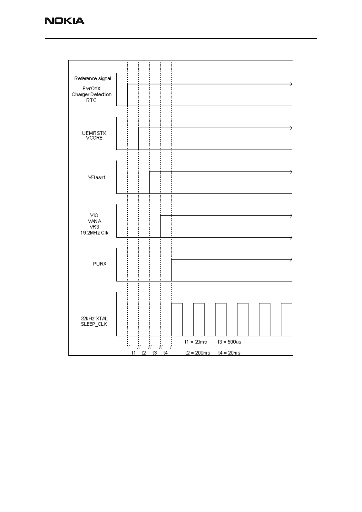
The following timing diagram represents the UEM start-up sequence from reset to
power-on mode.
Page 6 ©2004 Nokia Corporation Company Confidential Issue 1 07/2004
Page 7
2112 (RH-57)
Nokia Customer Care Troubleshooting — BB
Figure 2: Power-on sequence and timing
Issue 1 07/2004 ©2004 Nokia Corporation Company Confidential Page 7
Page 8
2112 (RH-57)
Troubleshooting — BB Nokia Customer Care
Power Up - Power Key
When the power key is pressed, the UEM enters the power-up sequence. Pressing the
power key causes the PWRONX pin on the UEM to be grounded. The UEM PWRONX
signal is not part of the keypad matrix. The power key is only connected to the UEM. This
means that when pressing the power key an interrupt is generated to the UPP that starts
the MCU. The MCU then reads the UEM interrupt register and notices that it is a
PWRONX interrupt. The MCU reads the status of the PWRONX signal using the UEM
control bus (CBUS). If the PWRONX signal stays low for a certain time the MCU accepts
this as a valid power-on state and continues with the SW initialization of the baseband.
If the power key does not indicate a valid power-on situation, the MCU powers off the
baseband.
Power Up - Charger
In order to be able to detect and start charging in cases where the main battery is fully
discharged (empty) and hence UEM has no supply (NO_SUPPLY or BACKUP mode of
UEM), charging is controlled by start-up charging circuitry.
Whenever the VBAT level is detected to be below the master reset threshold (V
charging is controlled by START_UP charge circuitry. Connecting a charger forces the
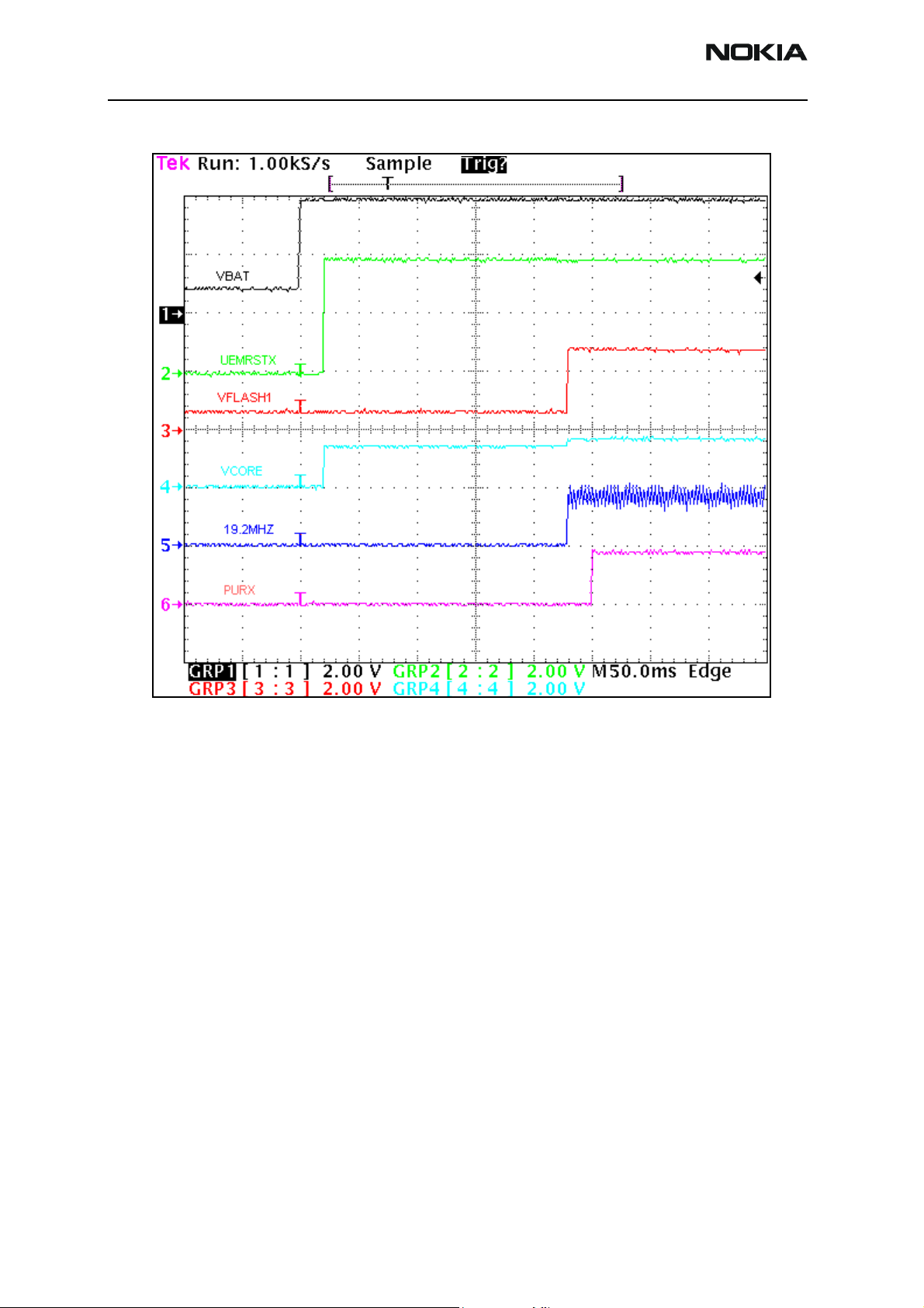
Figure 3: Measured power-on sequence and timing
MSTR-
),
Page 8 ©2004 Nokia Corporation Company Confidential Issue 1 07/2004
Page 9

2112 (RH-57)
Nokia Customer Care Troubleshooting — BB
VCHAR input to rise above the charger detection threshold (VCH
start-up charging is initiated. The UEM generates 100 mA constant output current from
the connected charger’s output voltage. The battery’s voltage rises at it charges, and
when the VBAT voltage level is detected to be higher than master reset threshold limit
(V
), the START_UP charge is terminated.
MSTR+
Monitoring the VBAT voltage level is done by charge control block (CHACON). A
MSTRX=‘1’ output reset signal (internal to the UEM) is given to the UEM’s reset block
when the VBAT>V
If the VBAT is detected to fall below V
cancelled. It will restart if a new rising edge on VCHAR input is detected (VCHAR rising
above VCH
DET+
Power Up - RTC Alarm
If phone is in POWER_OFF mode when RTC alarm occurs, the wake-up procedure occurs.
After the baseband is powered on, an interrupt is given to MCU. When an RTC alarm
occurs during ACTIVE mode, the interrupt is generated to the MCU.
Power Off
).
and the UEM enters into the reset sequence.
MSTR+
during start-up charging, charging is
MSTR
) and by detection,
DET+
The baseband switches to power-off mode if any of following occurs:
• Power key is pressed
• Battery voltage is too low (VBATT < 3.2 V)
• Watchdog timer register expires
The UEM controls the power-down procedure.
Power Consumption and Operation Modes
In POWER-OFF mode, the power (VBAT) is supplied to the UEM, vibra, LED, PA, and PA
drivers (Tomcat and Hornet). During this mode, the current consumption is approximately
35 uA.
In the SLEEP mode, both processors (MCU and DSP) are in stand-by mode. The phone
enters sleep mode only when both processors make this request. When the SLEEPX signal
is detected low by the UEM, the phone enters sleep mode. The VIO and VFLASH1
regulators are put into low quiescent current mode, VCORE enters LDO mode, and the
VANA and VFLASH2 regulators are disabled. All RF regulators are disabled during sleep
mode. When the SLEEPX signal is detected high by the UEM, the phone enters ACTIVE
mode and all functions are activated.
Sleep mode is exited either by the expiration of a sleep clock counter in the UEM or by
some external interrupt (generated by a charger connection, key press, headset
connection, etc.).
Issue 1 07/2004 ©2004 Nokia Corporation Company Confidential Page 9
Page 10

2112 (RH-57)
Troubleshooting — BB Nokia Customer Care
In sleep mode, the VCTCXO is shut down and the 32 kHz sleep clock oscillator is used as
a reference clock for the baseband.
In ACTIVE mode, the phone is in normal operation, scanning for channels, listening to a
base station, transmitting and processing information. There are several sub-states in the
active mode depending on the phone present state of the phone, such as burst reception,
burst transmission, if the DSP is working, etc.
In active mode, SW controls the UEM RF regulators: VR1A and VR1B can be enabled or
disabled. VSIM can be enabled or disabled and its output voltage can be programmed to
be 1.8 V or 3.3 V. VR2 and VR4—VR7 can be enabled or disabled or forced into low
quiescent current mode. VR3 is always enabled in active mode and disabled during Sleep
mode and cannot be control by SW in the same way as the other regulators. VR3 will
only turn off if both processors request to be in sleep mode.
CHARGING mode can be performed in parallel with any other operating mode. A BSI
resistor inside the battery pack indicates the battery type/size. The resistor value
corresponds to a specific battery capacity. This capacity value is related to the battery
technology.
The battery voltage, temperature, size, and charging current are measured by the UEM,
and the charging software running in the UPP controls it.
The charging control circuitry (CHACON) inside the UEM controls the charging current
delivered from the charger to the battery and phone. The battery voltage rise is limited
by turning the UEM switch off when the battery voltage has reached 4.2 V. The charging
current is monitored by measuring the voltage drop across a 220 mOhm resistor.
Power Distribution
In normal operation, the baseband is powered from the phone‘s battery. The battery
consists of one Lithium-Ion cell capacity of 850 mAh and some safety and protection
circuits to prevent harm to the battery.
The UEM ASIC controls the power distribution to the whole phone through the BB and RF
regulators excluding the power amplifier (PA), which has a continuous power rail directly
from the battery. The battery feeds power directly to the following parts of the system:
•UEM
•PA
•Vibra
•Display
• Keyboard lights
The heart of the power distribution to the phone is the power control block inside the
UEM. It includes all the voltage regulators and feeds the power to the whole system. The
UEM handles hardware power-up functions so the regulators are not powered and the
power up reset (PURX) is not released if the battery voltage is less than 3 V.
Page 10 ©2004 Nokia Corporation Company Confidential Issue 1 07/2004
Page 11
2112 (RH-57)
Nokia Customer Care Troubleshooting — BB
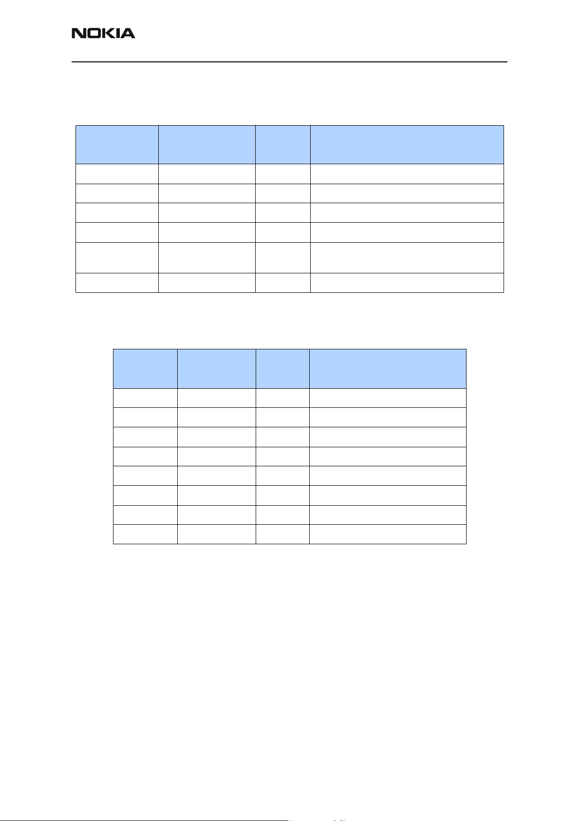
The 2112 baseband is powered from five different UEM regulators (see Table 1).
Table 1: Baseband Regulators
Regulator
VCORE 300 1.57/1.35 Power up default 1.57V and 1.35 in Sleep Mode.
VIO 150 1.8 Enabled always except during power-off mode
VFLASH1 70 2.78 Enabled always except during power-off mode
VFLASH2 40 2.78 Enabled only when data cable is connected
VANA 80 2.78 Enabled only when the system is awake (Off
VSIM 25 3.0 Enabled only when SIM card is used
Maximum
Current (mA)
Vout (V) Notes
during sleep and power off-modes)
Table 2 includes the UEM regulators for the RF.
Table 2: RF Regulators
Regulator
VR1A 10 4.75 Enabled when cell transmitter is on
VR1B 10 4.75 Enabled when the transmitter is on
Maximum
Current (mA)
Vout (V) Notes
VR2 100 2.78 Enabled when the transmitter is on
VR3 20 2.78 Enabled when SleepX is high
VR4 50 2.78 Enabled when the receiver is on
VR5 50 2.78 Enabled when the receiver is on
VR6 50 2.78 Enabled when the transmitter is on
VR7 45 2.78 Enabled when the receiver is on
The charge pump that is used by VR1A is constructed around the UEM. The charge pump
works with the Cbus (1.2 MHz) oscillator and gives a 4.75 V regulated output voltage to
the RF.
Issue 1 07/2004 ©2004 Nokia Corporation Company Confidential Page 11
Page 12
2112 (RH-57)
Troubleshooting — BB Nokia Customer Care
Clock Distribution
RFClk (19.2 MHz Analog)
The main clock signal for the baseband is generated from the voltage and temperature
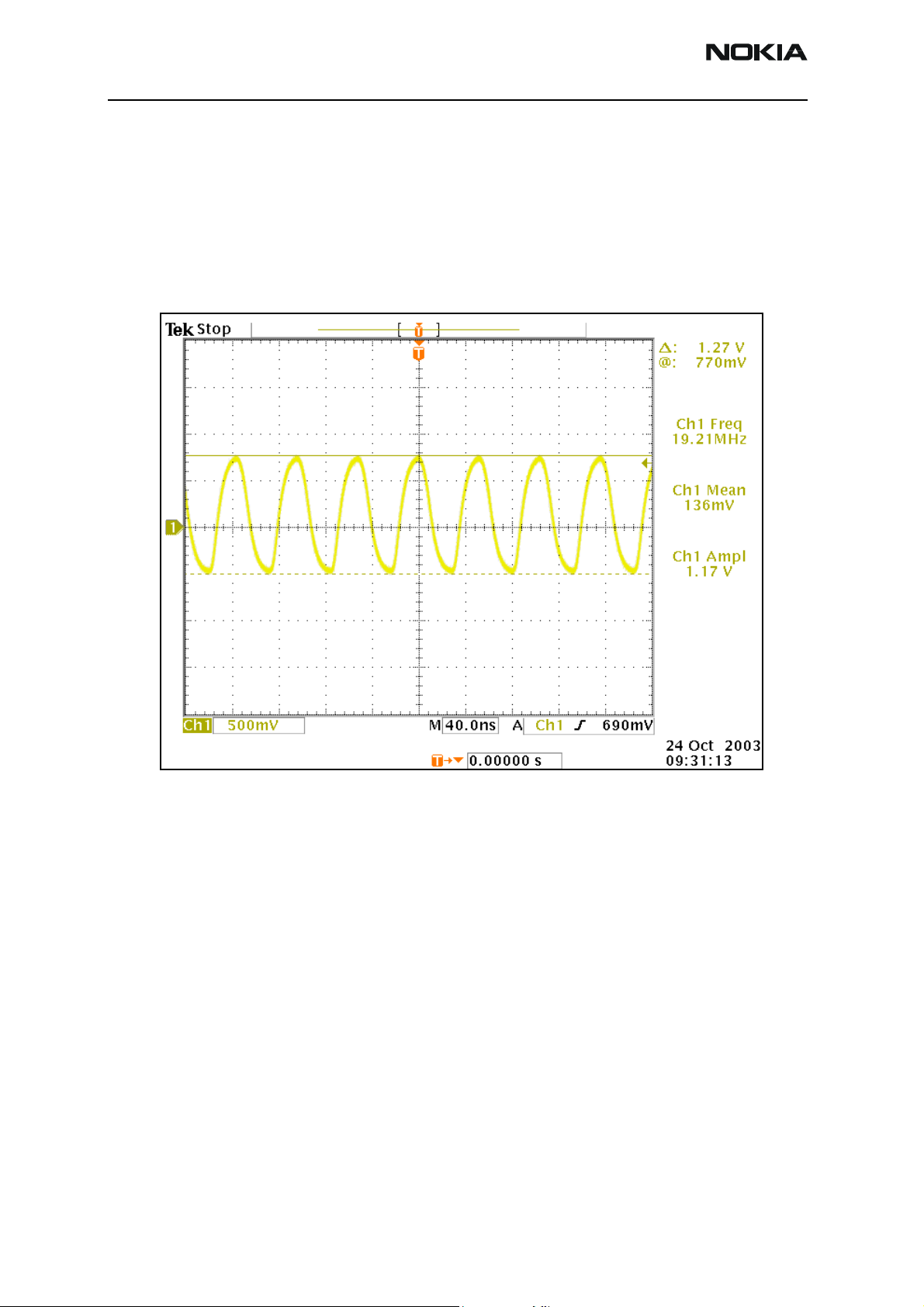
controlled crystal oscillator VCTCXO (G500). This 19.2 MHz clock signal is generated at
the RF and is fed to Yoda pin 18 (TCXO_IN). Yoda then converts the analog sine
waveform to a digital waveform with a swing voltage of 0 tot 1.8 V and sends it to the
UPP from pin 16 at Yoda (19.2 Out) to the UPP pin M5 (RFCLK).
Figure 4: Waveform of the 19.2 MHz clock (VCTCXO) going to the Yoda ASIC
Page 12 ©2004 Nokia Corporation Company Confidential Issue 1 07/2004
Page 13
2112 (RH-57)
Nokia Customer Care Troubleshooting — BB
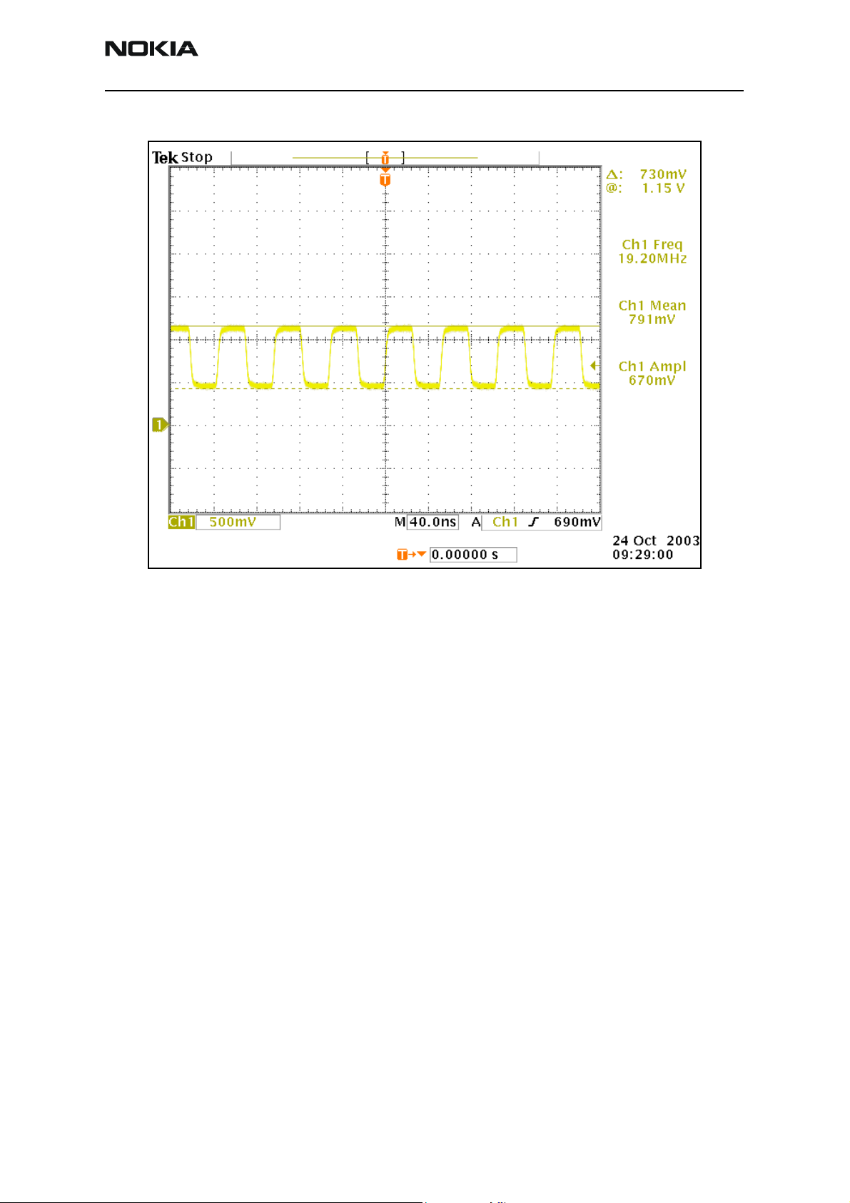
Figure 5 shows the RFCLK signal for the UPP.
Figure 5: Waveform of the 19.2 MHz Clk going to the UPP for Yoda ASIC at C711
Issue 1 07/2004 ©2004 Nokia Corporation Company Confidential Page 13
Page 14
2112 (RH-57)
Troubleshooting — BB Nokia Customer Care
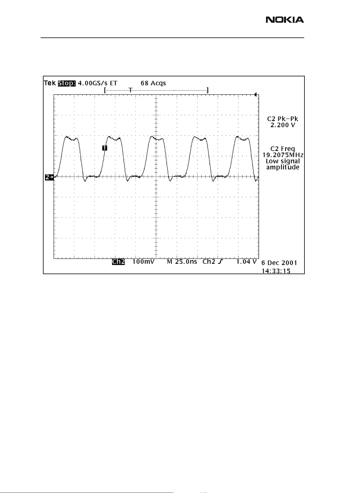
RFConvClk (19.2 MHz digital)
The UPP distributes the 19.2 MHz internal clock to the DSP and MCU, where the SW
multiplies this clock by seven for the DSP and by two for the MCU.
Figure 6: RFCovCLk waveform
Page 14 ©2004 Nokia Corporation Company Confidential Issue 1 07/2004
Page 15
2112 (RH-57)
Nokia Customer Care Troubleshooting — BB
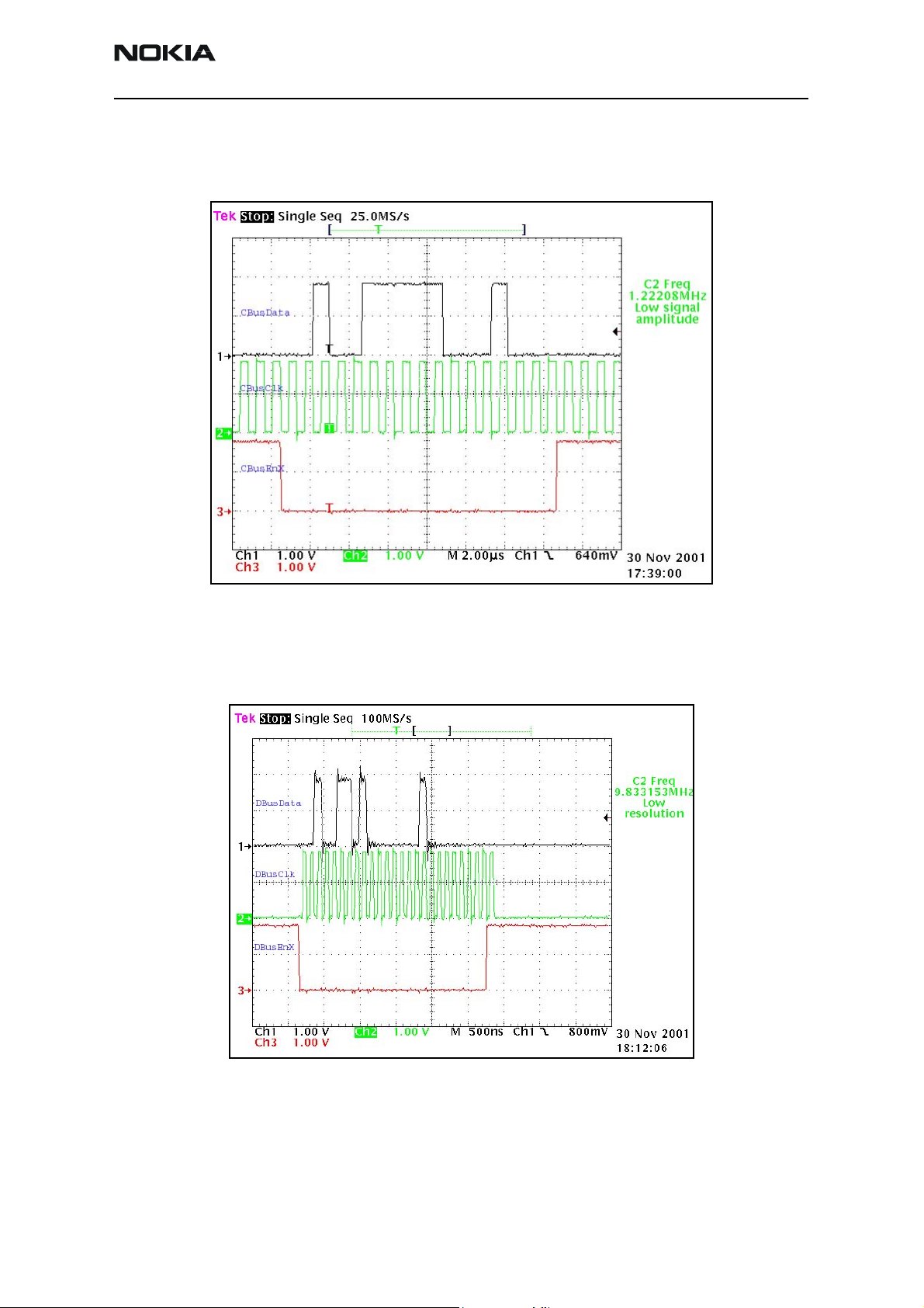
CBUS Clk Interface
A 1.2 MHz clock signal is used for CBUS, which is used by the MCU to transfer data
between the UEM and UPP.
DBUS Clk Interface
A 9.6 MHz clock signal is used for DBUS, which is used by the DSP to transfer data
between the UEM and UPP.
Figure 7: Cbus data transfer
Figure 8: Dbus data transferring
The system clock is stopped during sleep mode by disabling the VCTCXO power supply
(VR3) from the UEM regulator output by turning off the controlled output signal SleepX
from the UPP.
Issue 1 07/2004 ©2004 Nokia Corporation Company Confidential Page 15
Page 16

2112 (RH-57)
Troubleshooting — BB Nokia Customer Care
SleepCLK (Digital)
The UEM provides a 32 kHz sleep clock for internal use and to the UPP, where it is used
for sleep mode timing.
SleepCLK (Analog)
When the system enters sleep mode or power off mode, the external 32 KHz crystal
provides a reference to the UEM RTC circuit to turn on the phone during power off or
sleep mode.
Figure 9: 32 kHz Digital output from UEM
Figure 10: 32 kHz analog waveform at 32 KHz crystal input
Page 16 ©2004 Nokia Corporation Company Confidential Issue 1 07/2004
Page 17

2112 (RH-57)
Nokia Customer Care Troubleshooting — BB
Flash Programming
Connections to Baseband
The flash programming equipment is connected to the baseband using test pads for
galvanic connection. The test pads are allocated in such a way that they can be accessed
when the phone is assembled. The flash programming interface uses the VPP, FBUSTX,
FBUSRX, MBUS, and BSI connections for the connection to the baseband. The connection
is through the UEM, which means that the logic levels corresponding to 2.78 V. Power is
supplied using the battery contacts.
Baseband Power Up
The baseband power is controlled by the flash prommer in production and in
reprogramming situations. The baseband powers up by applying supply voltage to the
battery terminals. Once the baseband is powered, flash programming indication begins
(see the following "Flash Programming Indication" section).
Flash Programming Indication
Flash programming is indicated to the UPP using the MBUSRX signal between the UPP
and UEM. The MBUS signal from the baseband to the flash prommer is used as a clock
for the synchronous communication. The flash prommer keeps the MBUS line low during
UPP boot to indicate that the flash prommer is connected. If the UPP MBUSRX signal is
low on UPP, the MCU enters flash programming mode. In order to avoid accidental entry
to the flash-programming mode, the MCU waits for a specified time to get input data
from the flash prommer. If the timer expires without any data being received, the MCU
continues the boot sequence. The MBUS signal from the UEM to the external connection
is used as a clock during flash programming. This means that the flash-programming
clock is supplied to the UPP on the MBUSRX signal.
The flash prommer indicates flash programming/reprogramming to the UEM by writing
an 8-bit password to the UEM. The data is transmitted on the FBUSRX line and the UEM
clocks the data on the FBUSRX line into a shift register. When the 8 bits have been
shifted in the register, the flash prommer generates a falling edge on the BSI line. This
loads the shift register content in the UEM into a compare register. If the 8 bits in the
compare register matches with the default value preset in the UEM, the flash prommer
pulls the MBUS signal to UEM low in order to indicate to the MCU that the flash
prommer is connected. The UEM reset state machine performs a reset to the system,
PURX low for 20 ms. The UEM flash programming mode is valid until the MCU sets a bit
in the UEM register that indicates the end of flash programming. Setting this bit also
clears the compare register in the UEM, which was loaded at the falling edge of the BSI
signal. The UEM watchdogs are disabled during the flash programming mode. Setting the
bit indicating the end of flash programming enables and resets the UEM watchdog timer
to its default value. Clearing the flash programming bit also causes the UEM to generate
a reset to the UPP.
Issue 1 07/2004 ©2004 Nokia Corporation Company Confidential Page 17
Page 18

2112 (RH-57)
Troubleshooting — BB Nokia Customer Care
The BSI signal is used to load the value into the compare register. In order to avoid
spurious loading of the register, the BSI signal is gated during UEM master reset and
during power on when PURX is active. The BSI signal should not change states during
normal operation unless the battery is extracted. In this case, the BSI signal will be
pulled high. Note that a falling edge is required to load the compare register.
Flashing
Flash programming is done through the VPP, FBUSTX, FBUSRX, MBUS, and BSI signals.
When the phone enters the flash programming mode, the prommer indicates to the UEM
that flash programming will take place by writing an 8-bit password to the UEM. The
prommer sets the BSI value to “1” and then uses FBUSRX for writing and MBUS for
clocking. The BSI is then set back to “0”.
The MCU uses the FBUSTX signal to indicates to the prommer that it has been noticed.
After this, it reports the UPP type ID and is ready to receive the secondary boot code to
its internal SRAM.
FLASH_1
CH1 = BSI
CH2 = MBUS
CH3 = FBUSTX
CH4 = FBUSRX
Measure points
Production test pattern
(J396)
Figure 11: Flashing starts by BSI being pulled up and password being sent to UEM
This boot code asks the MCU to report the phone’s configuration information to the
prommer, including the flash device type. The prommer can then select and send
algorithm code to the MCU SRAM (and SRAM/Flash self-tests can be executed).
Page 18 ©2004 Nokia Corporation Company Confidential Issue 1 07/2004
Page 19

2112 (RH-57)
Nokia Customer Care Troubleshooting — BB
FLASH_2
CH1 = PURX
CH2 = MBUS
CH3 = FBUSTX
CH4 = FBUSRX
Measure points
Produc tio n te s t pa tter n
(J396)
Figure 12: Flashing, continued
Channel 2 (MBUS) is toggled three times for MCU initialization. At Channel 3 (FBUSTX)
low, the MCU indicates that the prommer has been noticed.
FLASH_3
CH1 = PURX
CH2 = MBUS
CH3 = FBUSTX
CH4 = FBUSRX
Measure points
Produc tio n te s t pa tter n
(J396)
Data transfer has
started (Fbus_Rx)
Figure 13: Flashing, continued 2
Issue 1 07/2004 ©2004 Nokia Corporation Company Confidential Page 19
Page 20

2112 (RH-57)
Troubleshooting — BB Nokia Customer Care
Flash Programming Error Codes
The following characteristics apply to the information in Table 3.
• Error codes can be seen from the test results or from Phoenix's flash-tool.
• Underlined information means that the connection under consideration is being
used for the first time.
Table 3: Flash Programming Error Codes
Error Description Not Working Properly
C101 "The Phone does not set FbusTx line high after
the startup."
C102 "The Phone does not set FbusTx line low after
the line has been high. The Prommer generates
this error also when the Phone is not connected to the Prommer."
C103 " Boot serial line fail." Mbus from Prommer->UEM->UPP(MbusRx)(SA1)
C104 "MCU ID message sending failed in the Phone." FbusTx from UPP->UEM->Prommer
C105 "The Phone has not received Secondary boot
codes length bytes correctly."
C106 "The Phone has not received Secondary code
bytes correctly."
C107 "The Phone MCU can not start Secondary code
correctly."
Vflash1
VBatt
BSI and FbusRX from prommer to UEM.
FbusTx from UPP->UEM->Prommer(SA0)
PURX(also to Safari)
VR3
Rfclock(VCTCXO->Safari->UPP)
Mbus from Prommer->UEM->UPP(MbusRx)(SA0)
FbusTx from UPP->UEM->Prommer(SA1)
BSI and FbusRX from prommer to UEM.
FbusRx from Prommer->UEM->UPP
FbusTx from UPP->UEM->Prommer
Mbus from Prommer->UEM->UPP(MbusRx)
FbusRx from Prommer->UEM->UPP
FbusTx from UPP->UEM->Prommer
Mbus from Prommer->UEM->UPP(MbusRx)
FbusRx from Prommer->UEM->UPP
FbusTx from UPP->UEM->Prommer
UPP
C586 "The erasing status response from the Phone
informs about fail."
C686 "The programming status response from the
Phone informs about fail."
Cx81 "The Prommer has detected a checksum error
in the message, which it has received from the
Phone."
Cx82 "The Prommer has detected a wrong ID byte in
the message, which it has received from the
Phone."
Flash
Flash
FbusTx from UPP->UEM->Prommer
FbusTx from UPP->UEM->Prommer
Page 20 ©2004 Nokia Corporation Company Confidential Issue 1 07/2004
Page 21

2112 (RH-57)
Nokia Customer Care Troubleshooting — BB
Table 3: Flash Programming Error Codes (Continued)
Error Description Not Working Properly
A204
Cx83
Cx84
Cx85
Cx87 "Wrong MCU ID." RFClock
Startup
for
flashing
"The flash manufacturer and device IDs in the
existing algorithm files do not match with the
IDs received from the target phone."
"The Prommer has not received phone
acknowledge to the message."
"The phone has generated NAK signal during
data block transfer."
"Data block handling timeout"
Required startup for flashing Vflash1
Flash
UPP
VIO/VANA
Signals between UPP-Flash
Mbus from Prommer->UEM->UPP(MbusRx)
FbusRx from Prommer->UEM->UPP
FbusTx from UPP->UEM->Prommer
UPP(Vcore)
VBatt
Charging Operation
Battery
The 2112 uses a Lithium-Ion cell battery with a capacity of 850 mAh. Reading a resistor
inside the battery pack on the BSI line indicates the battery size. The phone measures the
approximate temperature of the battery on the BTEMP line with an NTC resistor on the
PCB.
The temperature and capacity information are needed for charge control. These resistors
are connected to the BSI pin of the battery connector and the BTEMP of the phone. The
phone has 100 kΩ pull-up resistors for this line so that they can be read by A/D inputs in
the phone.
Charging Circuitry
The UEM ASIC controls charging depending on the charger being used and the battery
size. External components are needed for EMC, reverse polarity, and transient protection
of the input to the baseband module. The charger connection is through the system
connector interface. The baseband is designed to support DCT3 chargers from an
electrical point of view. Both 2- and 3-wire type chargers are supported. However, the
3-wire chargers are treated as a 2-wire charger.
Figure 14: BL-5C battery pack pin order
Issue 1 07/2004 ©2004 Nokia Corporation Company Confidential Page 21
Page 22

2112 (RH-57)
y
Troubleshooting — BB Nokia Customer Care
R200
V100 batter
Charger Detection
Connecting a charger creates voltage on the VCHAR input of the UEM. Charging starts
when the UEM detects the VCHAR input voltage level above 2 V (VCHdet+ threshold).
The VCHARDET signal is generated to indicate the presence of the charger for the SW.
The EM SW controls the charger identification/acceptance. The charger recognition is
initiated when the EM SW receives a ”charger connected” interrupt. The algorithm
basically consists of the following three steps:
1. Check that the charger output (voltage and current) is within safety limits.
2. Identify the charger as a two-wire or three-wire charger.
3. Check that the charger is within the charger window (voltage and current).
If the charger is accepted and identified, the appropriate charging algorithm is initiated.
X102
1
F100
1.5A
Figure 15: Charging circuitry
L1002
________
42R/100MHz
V100
"VCHARIN"
C106
1n0
0
2
CHARGER(4:0)
Figure 16: Charging circuit
Page 22 ©2004 Nokia Corporation Company Confidential Issue 1 07/2004
Page 23

2112 (RH-57)
Nokia Customer Care Troubleshooting — BB
Charge Control
In active mode, charging is controlled by the UEM’s digital part. Charging voltage and
current monitoring is used to limit charging into safe area. For this reason, the UEM has
the following programmable charge cut-off limits:
• VBATLim1=3.6 V (Default)
• VBATLim2L=5.0 V
• VBATLim2H=5.25 V
VBATLim1, 2L, 2H are designed with hystereses. When the voltage rises above VBATLim1,
2L, 2H+ charging is stopped by turning the charging switch off. No change is done in
operational mode. After the voltage has decreased below VBATLim-, charging restarts.
There are two PWM frequencies in use depending on the type of the charger. A 2-wire
charger uses a 1 Hz, while a 3-wire charger uses a 32Hz. The duty cycle range is 0% to
100%. The maximum charging current is limited to 1.2 A.
UEM Pins
N10
R200
VBAT
M10
Audio
.22 Ohms
C201
1uF
Figure 17: Charging circuity at the battery
C202
10nF
The audio control and processing is provided by UEM, which contains the audio codec,
and the UPP, which contains the MCU and DSP blocks. These blocks handle and process
the audio data signals.
The baseband supports three microphone inputs and two earpiece outputs. The
microphone inputs are MIC1, MIC2, and MIC3. MIC1 input is used for the phone's
internal microphone; MIC2 input is used for headsets (HDB-4). MIC3 is not used. Every
microphone input can have either a differential or single-ended AC connection to UEM
circuit. The internal microphone (MIC1) and external microphone (MIC2) for Tomahawk
accessory detection are both differential. The microphone signals from different sources
are connected to separate inputs at UEM. Inputs for the microphone signals are
differential types. Also, MICBIAS1 is used for MIC1 and MICBIAS2 is used for MIC2. The
2112 also supports a hands-free speaker (B301), which is driven by an IHF audio amplifier
(N150).
Display and Keyboard
The 2112 uses LEDs for LCD and keypad illumination. There is one LED for the LCD and
four LEDs for the keypad. KLIGHT is the signal used to drive the LED driver for the LCD
and keyboard. This signal turns on the LED driver (N302).
Issue 1 07/2004 ©2004 Nokia Corporation Company Confidential Page 23
Page 24

2112 (RH-57)
Troubleshooting — BB Nokia Customer Care
The 2112 also uses an IOS LCD. The interface uses a 9-bit data transfer and is quite
similar to the DCT3 type interface, except the Command/Data information is transferred
together with the data.
Flashlight
The flashlight is driven by the white LED driver and controlled by the UEM. The
TK65600B-G is an active-high enable device, which is tied to the DLIGHT signal from the
UEM.
Accessories
The 2112 supports Tomahawk and Universal Headset accessories, differential and singleended, respectively. Detection of the Tomahawk accessories is done through the ACI
signal where the Universal Headset is detected on GenIO (12).
Figure 18: Waveform for the LCD Interface
Figure 19: Tomahawk connector pin out
Page 24 ©2004 Nokia Corporation Company Confidential Issue 1 07/2004
Page 25

2112 (RH-57)
Nokia Customer Care Troubleshooting — BB
The pin out on the Tomahawk connector is as follows:
•Charger
• Charger GND
•ACI
•Vout
•USB Vbus
• USB D+ / Fbus Rx
• USB D- / Fbus Tx
• Data GND
•XMic N
•XMic P
•HSear N
You can perform the following in Tomahawk accessories:
Charging
Charging through Tomahawk is accomplished in the same manner as through the
charger connector. Pin 1 of the Tomahawk is physically connected to the charger
connector. When the phone is connected to a desktop charger (e.g., DCV-15), it charges
in the same manner as it does with the charger connector.
Figure 20 shows the actual charging sequence. The channels on the diagram are:
•HSear P
•HSear R N
•HSear R P
• Charging
• Accessory detection
• FBUS communication
• Fully differential audio interface for mono- and stereo outputs
• CH1 = Charging current across the .22 Ohm (R200) resistor on UEMK
• CH2 = Charger voltage measure at V100
• CH3 = Battery voltage measure at R200
•CH4 = PURX
Issue 1 07/2004 ©2004 Nokia Corporation Company Confidential Page 25
Page 26

2112 (RH-57)
Troubleshooting — BB Nokia Customer Care
In Channel 4, PURX is released, which this indicates when the phone operation goes from
RESET mode to POWER_ON mode.
Tomahawk Headset Detection
Accessory detection on the Tomahawk is done digitally. The pins used for this accessory
detection are:
• Pin 2 (Charge GND)
• Pin 3 (ACI)
•Pin 4 (Vout)
Figure 20: Charging sequence
Page 26 ©2004 Nokia Corporation Company Confidential Issue 1 07/2004
Page 27

2112 (RH-57)
Nokia Customer Care Troubleshooting — BB
FBus Detection
FBus communication in Tomahawk is done through the following lines:
• Pin 2 (Charge GND)
• Pin 3 (ACI)
•Pin 4 (Vout)
• Pin 6 (FBus Rx)
• Pin 7 (FBus Tx)
Figure 21: Waveform showing Tomahawk accessory detection
Issue 1 07/2004 ©2004 Nokia Corporation Company Confidential Page 27
Page 28

2112 (RH-57)
Troubleshooting — BB Nokia Customer Care
Figure 22: Waveform showing Tomahawk FBus communication
Accessory Detection Through ACI
USB and Audio on (mono or stereo)/FM radio communication in Tomahawk is done
through the following signals:
Table 4: Accessory Detection Signals
USB Audio/FM
Pin 5 (USB Vbus) Pin 9 (XMic N)
Pin 6 (USB +) Pin 10 (SMIC P)
Pin 7 (USB -) Pin 11 (HSEAR N)
Pin 8 (Data GND) Pin 12 (HSEAR P)
Pin 13 (HSEAR R N)
Pin 14 (HSEAR R P)
Page 28 ©2004 Nokia Corporation Company Confidential Issue 1 07/2004
Page 29

2112 (RH-57)
Nokia Customer Care Troubleshooting — BB
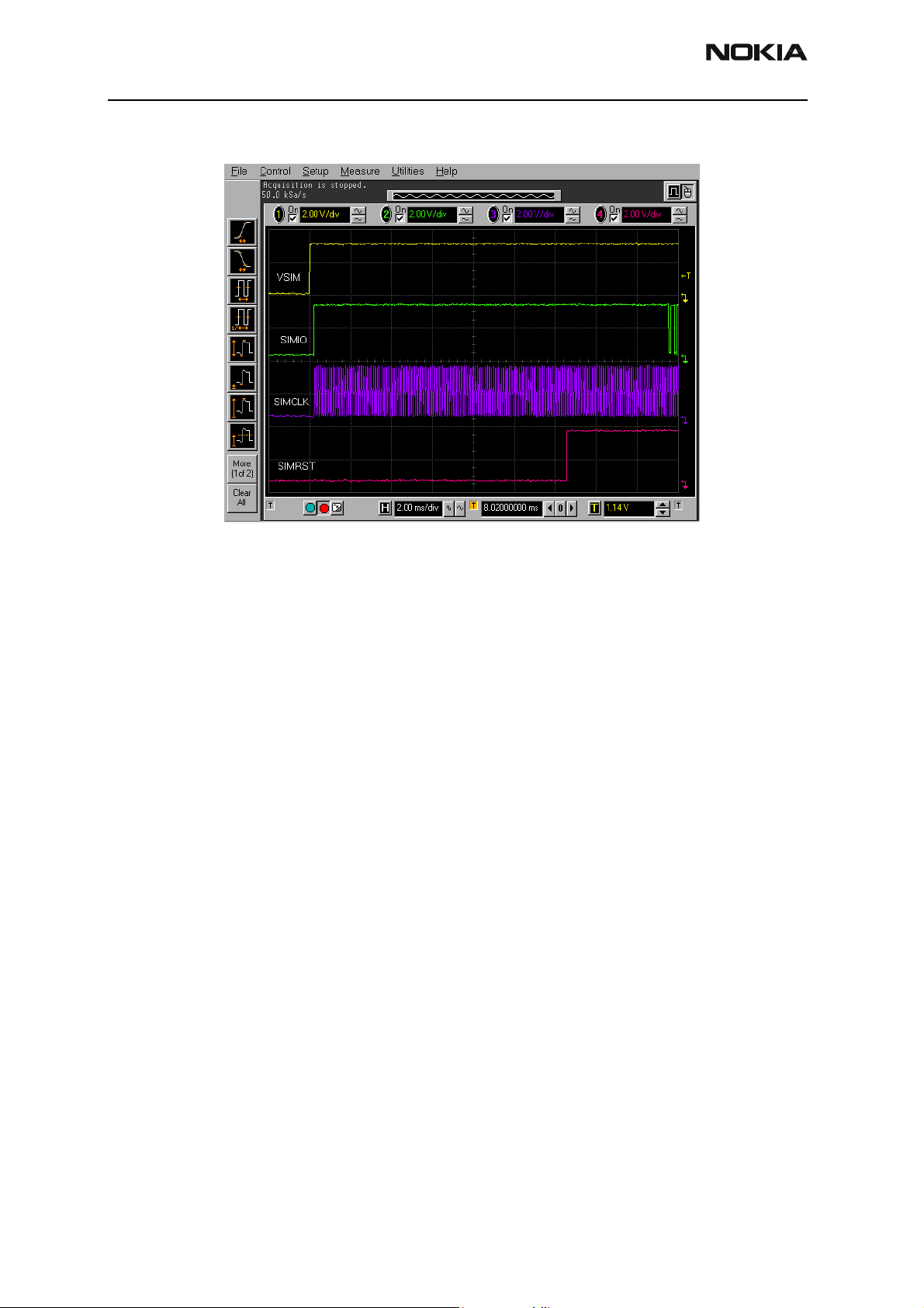
SIM CAR
The 2112 supports SIM CAR. Use the waveform in Figure 24 to verify that the sim_vcc,
sim_i/o, cim_clk, and sim_rst signals are activated in the correct sequence at power up.
This picture may be taken when the SIM CAR is installed on the phone to measure the
signals when the phone is turned on. The figure shows the proper waveforms when the
interface is working. See Figure 26 on page 32 for the test point’s location.
Figure 23: Waveform showing accessory detection through ACI
Issue 1 07/2004 ©2004 Nokia Corporation Company Confidential Page 29
Page 30
2112 (RH-57)
Troubleshooting — BB Nokia Customer Care
Figure 24: RUIM signal waveform
Page 30 ©2004 Nokia Corporation Company Confidential Issue 1 07/2004
Page 31

2112 (RH-57)
Nokia Customer Care Troubleshooting — BB
Test Points
Figure 25: Test points (bottom)
Issue 1 07/2004 ©2004 Nokia Corporation Company Confidential Page 31
Page 32

2112 (RH-57)
Troubleshooting — BB Nokia Customer Care
Figure 26: BB test points (top)
Page 32 ©2004 Nokia Corporation Company Confidential Issue 1 07/2004
Page 33

2112 (RH-57)
Nokia Customer Care Troubleshooting — BB
Troubleshooting
The following hints should help finding the cause of the problem when the circuitry
seems to be faulty. Troubleshooting instructions are divided into the following sections:
• Top troubleshooting map
• Phone is totally dead
• Power does not stay on or the phone is jammed
• Flash programming does not work
• Display is not working
• Audio fault
• Charging fault
First, carry out a through visual check of the module. Ensure in particular that:
• There are no mechanical damages
• Soldered joints are okay
• ASIC orientations are okay
Issue 1 07/2004 ©2004 Nokia Corporation Company Confidential Page 33
Page 34

2112 (RH-57)
Troubleshooting — BB Nokia Customer Care
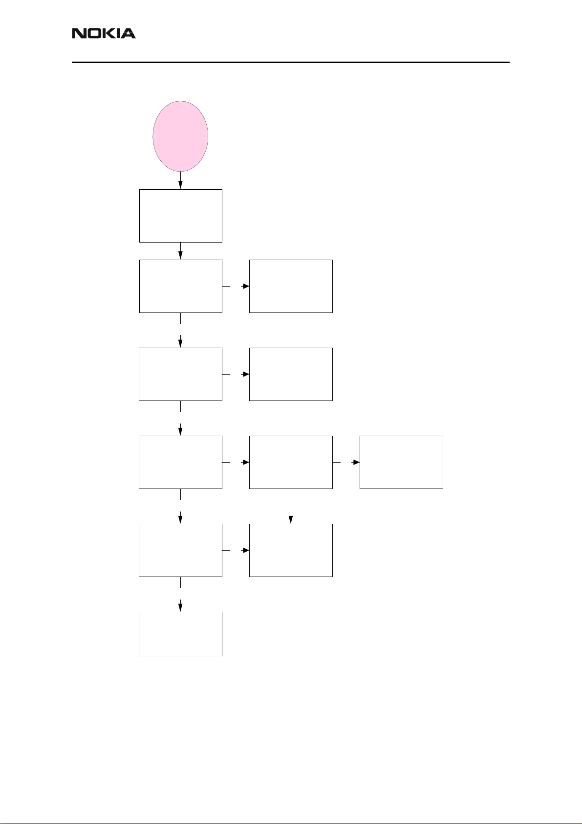
Top Troubleshooting Map
Top
P hone totally dead
NO
Flas h programming
does n't work
NO
P hone does n't start
up or phone is
jammed
NO
YES
YES
YES
Phone
dead
Flash
faults
Phone is
jammed
C harging does n't
work
NO
YES
Top page 2
Charger
faults
Page 34 ©2004 Nokia Corporation Company Confidential Issue 1 07/2004
Page 35

2112 (RH-57)
Nokia Customer Care Troubleshooting — BB
Top 2
Audio faults
NO
Dis play o r L E Ds not
working
NO
Keypad doesn't work
YES
YES
YES
Audio
faults
Dis play
faults
Keypad
faults
END
Issue 1 07/2004 ©2004 Nokia Corporation Company Confidential Page 35
Page 36

2112 (RH-57)
Troubleshooting — BB Nokia Customer Care
Phone is Totally Dead
¾ If current is zero , che ck the battery connector
Phone is
dead
to make sure Vbat makes contact.
¾ If current is too hig h, ch eck for shor ts.
¾ Make sure all BB regulators are at their
respective voltage levels (VANA, VIO,
VCORE, VFlash1, and VR3). See phone's top
view diagram for test point s.
Phone current is
zero or too high?
NO
Phone current is
<=30 mA
NO
Phone current is
35 mA
YES
YES
YES
NO
¾ Make sure the system Cl k i s 19. 2MHz and tha t
the sleep Clk is 32K H z
¾ Make sure PURX and SleepX signals are high
(1.8V)
Is phone flash
programming OK?
NO
YES
Phone is
jammed
Flash
faults
Is phone in Local
Mode?
YES
Check BSI line X103,
NO YES
R202, R206, C100,
C111. Are they OK?
NO
Change UEM
Repair
OK restart
Page 36 ©2004 Nokia Corporation Company Confidential Issue 1 07/2004
Page 37

2112 (RH-57)
Nokia Customer Care Troubleshooting — BB
Flash Programming Does Not Work
Flash
faults
The phone does not
set Flashbus TXD
line high after the
startup
NO
The phone does not
set Flashbus TXD
line low after the line
has been high
Change
UEM
YES
Measure BSI pulse during
YES NO
Flash programming. Is it
OK?
YES
Measure FBusRX (2.78V)
signal during flash
programming from
NO
production pattern. Is it
OK?
YES
Measure test point
FBusTx (J411) (1.8V) and
production pattern signal
NO
FBusTxO (2.78V) during
flash programming. Are
they the same?
YES
Check BSI line X103,
R202, R206, C100,
C111, C240
Reflow or
change UEM
Change UPP
NO
Is there a pulse
on J411?
YES
Is there a pulse
on FBusTx?
NO
Flash
faults,
page 2
YES
Measure MBus (2.78V). Is
it OK?
NO
NO
Reflow or
change UEM
Reflow or
change UEM
Issue 1 07/2004 ©2004 Nokia Corporation Company Confidential Page 37
Page 38

2112 (RH-57)
Troubleshooting — BB Nokia Customer Care
Flash
faults,
page 2
Can you read the
manufacturer ID and
the device ID?
YES
Is the phone totally
dead?
NO
Phone doesn't start
up or the phone is
jammed
NO
Reflow or change
Flash
YES
YES
Phone
dead
Phone is
jammed
NO
Retest
Page 38 ©2004 Nokia Corporation Company Confidential Issue 1 07/2004
Page 39

2112 (RH-57)
Nokia Customer Care Troubleshooting — BB
Power Does Not Stay on or the Phone is Jammed
Phone is
jammed
Measure VIO,
VCORE, VFlash1,
VANA, and VR3
voltages. Are they
OK?
YES
Measure 32kHz
Sleep Clk from
testpoint. Is it OK?
YES
Measure 19.2MHz RF
Clk at testpoint
C510. Is it OK?
Check VBATT, VIO,
VCORE, VFlash1,
VANA, VR3 capacitors.
NO
NO NO
NO
Are they OK?
NO
Measure the 32kHz
Clk crystal. Is it OK?
YES
YES
Check BSI/BTEMP
lines and VBATT
lines. If OK, reflow
or change UEM
Repair
Change B200
Reflow or change
UEM
YES
Measure PURX and
SleepX at test points
J402 and J403. Are
they high (1.8V)?
YES
Phone is
jammed,
page 2
Measure the
19.2MHz Clk coming
from the VCTCXO at
C728 and C711. Is it
NO
OK?
YES
Check G502, C522, C521,
R517, R516. If OK, change
NO
G501. Check C728. If OK,
change N700.
Change UPP
Change UEM
Issue 1 07/2004 ©2004 Nokia Corporation Company Confidential Page 39
Page 40

2112 (RH-57)
Troubleshooting — BB Nokia Customer Care
Phone is
jammed,
page 2
Phone shutdown
after 32 seconds
NO
Measure DBusEN
interface signal at
test point J413. Is it
OK?
YES
YES
NO
Reflow or
change UPP.
Is the ESN present
in the phone?
YES
Has the phone been
fully erased and
reflashed for this
problem?
YES
Measure watchdog
signal at CBusEN
interface at test
point J406. Is it OK?
YES
NO
NO
NO
Rebuild the ESN
Perform a full
erase and reflash
the phone
Reflow or change
UPP and reflash.
Reflow or change
UEM and reflash.
Read phone info. Is
it OK?
YES
Retest
Measure FBusRxO
NO NO
signal during phone
info read. Is it OK?
YES
Measure FBusTx
NO
signal during phone
info read from test
point J411. Is it OK?
YES
Reflow or change
UEM.
Reflow or change
UPP.
Reflow or change
UEM.
Page 40 ©2004 Nokia Corporation Company Confidential Issue 1 07/2004
Page 41
2112 (RH-57)
Nokia Customer Care Troubleshooting — BB
Charger
Charger
fau lts
Connect Charger.
M ake su re battery is
connected.
Battery bar doesn't
w o r k ( s c ro ll)
YES
Measure voltage
o v er V 1 0 0 . Is it >3 .0
Vdc?
YES
Read BT EM P value.
Is it ~ 25C (0 3 19)?
YES
Rem ove (fuse) F100
and m easure
current.
Is it ~ 8 5 0 mA ?
NO
NO
NO
NO
Retest
Check DC jack,
F100, L100, V100,
C106
C h e c k N T C. Is it
OK?
YES
Change UEM
NO
Replace NTC
YES
Retest
Issue 1 07/2004 ©2004 Nokia Corporation Company Confidential Page 41
Page 42

2112 (RH-57)
Troubleshooting — BB Nokia Customer Care
Audio Faults
Audio
faults
Is the earpiece
working?
YES
NO YES
Change earpiece. Is
it working now?
NO
Set phone in Local Mode. Use
Phoenix Troubleshooting >
Phone Control > Phone State
Tab > select Local Mode > click
Execute. Then use Audio Test >
HP microphone in/HP speaker
out > Loop ON to enable the
earpiece. Inject a 1KHz sine
signal 200mVp-p on XMIC.
Is the signal coming
out of the UEM on
NO
EARP and EARN?
Retest
Check R178. If OK,
then change
earpiece.
YES
Check L102, R150,
R152, R155, R151,
Audio
faults,
page 2
C181, C153, C151,
C152, C156. If OK,
change UEM.
Page 42 ©2004 Nokia Corporation Company Confidential Issue 1 07/2004
Page 43

2112 (RH-57)
Nokia Customer Care Troubleshooting — BB
Audio
faults,
page 2
Is the
microphone
working?
YES
Change the
NO YES
microphone. Is it
working now?
NO
Set the phone in Local Mode.
Use Phoenix Troubleshooting >
Phone Control > Phone State
Tab > Select Local Mode >
Execute. Then use Audio Test >
HP microphone in/HP speaker
out > Loop On to enable
earpiece. Talk through the
microphone.
Measure MICB1
voltage from MICP
NO
pads. Is it ~2.1V?
Retest
Check
connections at
C180 and R170. If
OK, change UEM
Audio
faults,
page 3
YES
Is the signal going
to the UEM at MICP
and MICN at R170?
YES
Is the signal going
out of the UEM at
XEAR, pin 11 and 12
on the bottom
connector (X101)?
YES
Check connections
at R171, R172, R173,
NO
C171, C172, C169,
C179, C178. If OK,
change microphone
Check L103, R168,
NO
R105. If OK, change
UEM
Retest
Issue 1 07/2004 ©2004 Nokia Corporation Company Confidential Page 43
Page 44

2112 (RH-57)
Troubleshooting — BB Nokia Customer Care
Audio
faults,
page 3
Is interna l handsfr e e
speaker (IHF)
working?
YES
Select a ring tone
and measure signals
NO YES
at L150 and L151. Is
signal OK?
NO
Measure GenIO28. Is
it OK (1 .8 V )?
YES
NO
Set the phone in Local
Mode. Use Phoenix
Troubleshooting > P ho n e
Control > Phone State Tab >
select Local Mode >
Execute. Then use Audio
test > HP microphone in/Ext
Speaker out > Loop ON. To
enable IHF turn on GenIO
(10). Measure and check IHF
testpoints J150, J151. Is it
OK?
NO
Change B301
Change UPP
Change IHF
YES
Change the UPP
Audio
faults,
page 4
Page 44 ©2004 Nokia Corporation Company Confidential Issue 1 07/2004
Page 45

2112 (RH-57)
Nokia Customer Care Troubleshooting — BB
Audio
faults,
page 4
Measure VBATT
Is Vibra working?
NO NO
voltage pin 1 of
M300. Is it OK?
YES
Check VBATT line
YES
Use UI Menu > Profile > Normal >
Customize > Vibrating Alert > Select On
> then go back to Customize menu >
Ringing Tone > Try any ring tone and
vibra should work.
Measure the UEM
signal on pin 2 of
M300. Is the signal
NO
OK?
YES
Change the UEM
Change Vibra
END
Issue 1 07/2004 ©2004 Nokia Corporation Company Confidential Page 45
Page 46

2112 (RH-57)
Troubleshooting — BB Nokia Customer Care
Display Faults
Display
faults
Are the keyboard
LEDs turned on
when the phone is
turned on or when
making a phone
call?
NO YES
Measure VBATT
voltage at L301. Is it
okay?
NO
Check VBATT line
and C303, C316, and
L300.
YES
Display
faults 2
Measure the driver
signal from UEM at
J336. Is the signal
okay?
YES
NO
Change UEM
Check N302 driver
signal at C304. If not
OK, change N302.
Page 46 ©2004 Nokia Corporation Company Confidential Issue 1 07/2004
Page 47

2112 (RH-57)
Nokia Customer Care Troubleshooting — BB
Display
faults,
page 2
Does the Display
start?
YES
Try changing
NO YES
display module.
Does it work?
NO
Measure VIO and
Flash1.
NO
Check LCD signals
LCDCSX (pin5),
LCDCLK (pin4),
LCDSDA (pin3), and
NO
LCDRESX (pin2) at
X302. Signals OK?
Retest
Change UEM
Change UPP
YES
Change Display
END
Issue 1 07/2004 ©2004 Nokia Corporation Company Confidential Page 47
Page 48

2112 (RH-57)
Troubleshooting — BB Nokia Customer Care
Keypad Faults
Keypad
faults
Is the power key
working?
YES
Keypad
faults,
page 2
NO NO
Measure voltage at
YES
Measure voltage at
S300 when power
key is pressed. Is it
high?
NO
S302. Is it high?
Check S302. Is
YES
it OK?
Change S300
NO
Check S302, C310,
and R306. If OK,
change UEM
YES
Phone is
dead
Phone is
jammed
Page 48 ©2004 Nokia Corporation Company Confidential Issue 1 07/2004
Page 49

2112 (RH-57)
Nokia Customer Care Troubleshooting — BB
Keypad
faults ,
page 2
Are the UI modules
keys working?
YES
END
Change keypads
NO
module. Is it
working?
NO
Measure ROW 0-5
(P10-P15) signals
between UPP and
keypad at J325,
J320, J321, J322,
J323. Are they
~1.8V?
YES
Measure COL 1-5
(P1-P5) signals
between UPP and
keypad at J331,
J324, J337, J326,
J327, J328, J329. A re
they ~1.8V
YES
NO
NO
Retest
Make sure
there are no
shorts on
Z300. If OK,
change UPP
Make sure
there are no
shorts on
Z300. If OK,
change UPP
Issue 1 07/2004 ©2004 Nokia Corporation Company Confidential Page 49
Page 50

2112 (RH-57)
Troubleshooting — BB Nokia Customer Care
Flashlight
Flashlight
faults
Are the flashlight
LEDs turned on
when the phone is
turned and when
pressing the UP
key?
YES
Flashlight
OK
NO
Measure VBATT
voltage at R303. Is it
OK?
YES
Measure the driver
signal DLIGHT at
D301 J336, and
Q301. Is the signal
OK?
YES
Check VBATT line at
NO
the battery
connector
NO
Change the UEM
Check N302, L301,
L300, C316, C304,
R300, R302, R304,
Check solder joints
at D305. If bad,
replace LEDs.
R2310.
YES
Page 50 ©2004 Nokia Corporation Company Confidential Issue 1 07/2004
 Loading...