

Page 1

Nokia Customer Care
2112 (RH-57) Series Transceivers
Troubleshooting - RF
Issue 1 07/2004 Company Confidential ©2004 Nokia Corporation
Page 2

2112 (RH-57)
Troubleshooting - RF Nokia Customer Care
Contents Page
RF Troubleshooting......................................................................................................................................... 3
2112 General Troubleshooting Notes .................................................................................................... 3
Phone Components ..................................................................................................................................... 4
Phone Cannot Make a Call..................................................................................................................... 5
Transmitter Troubleshooting ....................................................................................................................6
Low Tx Power ............................................................................................................................................. 6
Cell Transmitter Setup............................................................................................................................. 7
Cell Transmitter Path ............................................................................................................................... 9
Cell Power Amplifier ............................................................................................................................. 13
Cell PMIC.................................................................................................................................................. 13
Cell IF/RF AGC and PA Control........................................................................................................... 15
Cell Power Detector .............................................................................................................................. 17
Tx System Block Diagram .................................................................................................................... 19
Receiver Troubleshooting ........................................................................................................................20
Rx IF........................................................................................................................................................... 20
Switching the Gain................................................................................................................................ 25
Rx RF.......................................................................................................................................................... 27
Rx AGC (Cell mode) ............................................................................................................................... 29
Receiver Block Diagram ....................................................................................................................... 31
Synthesizer Troubleshooting ..................................................................................................................32
Synthesizer Setup .................................................................................................................................. 32
VCTCXO Tuning....................................................................................................................................... 33
VCTCXO Reference Clock..................................................................................................................... 37
Synthesizer Block Diagram ................................................................................................................. 38
UHF Synthesizer ..................................................................................................................................... 39
Rx VHF....................................................................................................................................................... 40
Tx VHF ....................................................................................................................................................... 41
Tuning Descriptions ..................................................................................................................................43
Page 2 ©2004 Nokia Corporation Company Confidential Issue 1 07/2004
Page 3

2112 (RH-57)
Nokia Customer Care Troubleshooting - RF
RF Troubleshooting
2112 General Troubleshooting Notes
First check the RX AGC PDM value when troubleshooting the receiver. The AGC value
should be close to the typical values in the tables. The Rx AGC tries to keep a constant
amplitude at the output of the receiver chain. If the AGC value indicates an AGC gain
that is substantially higher than normal, the AGC is compensating for extra loss in
another component. If the AGC PDM values are normal but there is still a problem, check
the actual AGC voltages. RF probing at specific locations in the chain can help to
pinpoint the source of the problem.
Likewise, first check the measured output power and AGC values when troubleshooting
the transmitter, which give an indication of where to start probing.
Although the tables in this chapter include power levels for many combinations of AGC
values, it is generally only necessary to check one combination. The additional
information is provided for use in unexpected situations. Likewise, although probing
points and signal-level information are given for each point in the receiver and
transmitter chains, it is not necessary to probe each point on every phone — only the
suspected trouble spots.
Absolute power measurements were made with an Agilent (HP) 85024A active
high-impedance probe. Other probes may be used (make sure the probe is highimpedance so the measurement does not load the circuit), but they may have different
gains. Therefore, adjust the absolute measurements accordingly, especially if you are
using a probe attenuator.
Typically, the higher loss occurs at the band edges where a range is given for loss.
Probing is not a very accurate method to measure absolute power; therefore, you cannot
expect measured results to exactly match the numbers listed.
Power depends on the impedance of the circuit. For example, if a filter has a nominal loss
of 5 dB, straightforward probing on the input and output and then subtracting might not
result in 5 dB because the input impedance could be different from the output
impedance. Most components in the RF section have the same input and output
impedance (50ohms). Where this is not the case, absolute power is noted in the tables in
dBm rather than loss or gain in dB.
Inject a CW tone into the receiver when testing the CDMA receiver. The gains and losses
are the same for a CW signal as for the CDMA.
Note: After opening the shield lids, always replace them with new lids.
Issue 1 07/2004 ©2004 Nokia Corporation Company Confidential Page 3
Page 4
2112 (RH-57)
Troubleshooting - RF Nokia Customer Care
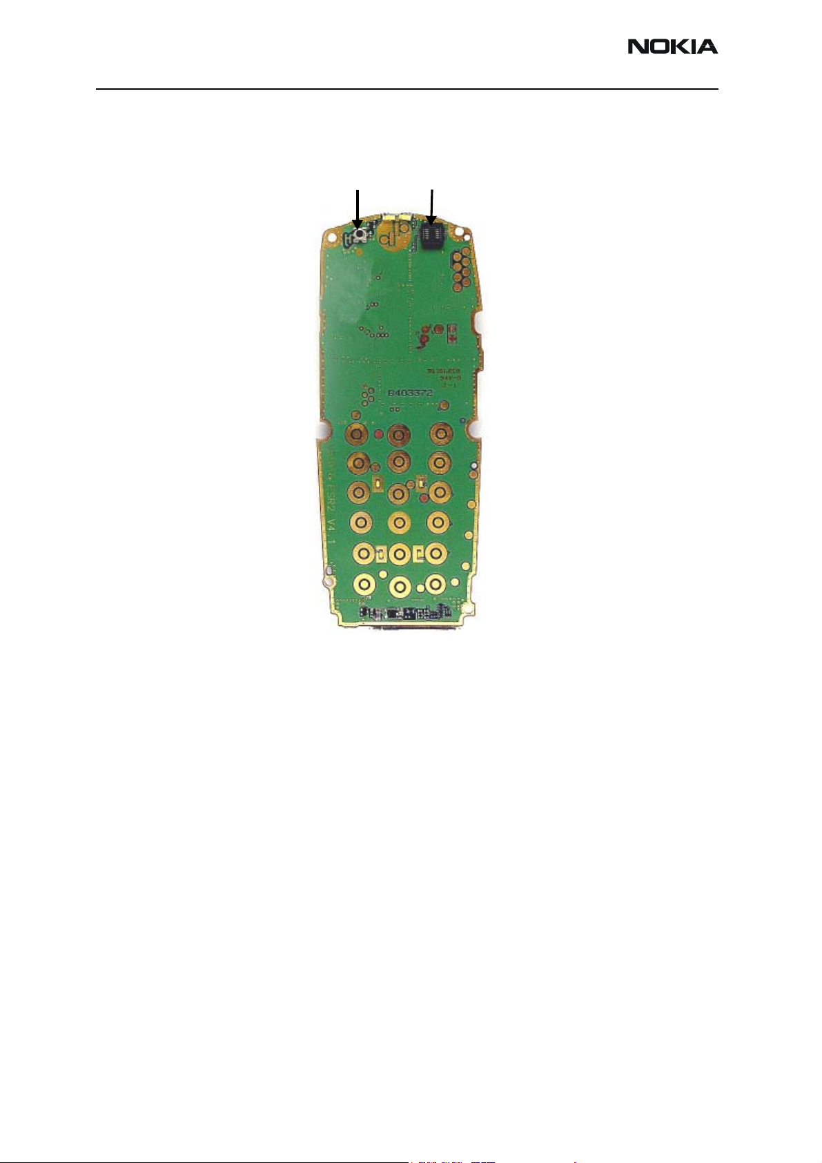
Phone Components
Figure 1 and Figure 2 illustrate the main components of the 2112.
RF connector LCD module connector
Figure 1: RF components (top)
Page 4 ©2004 Nokia Corporation Company Confidential Issue 1 07/2004
Page 5
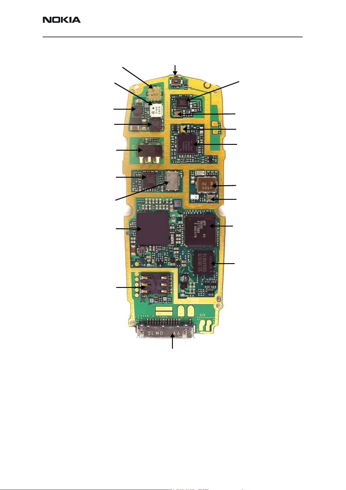
2112 (RH-57)
Nokia Customer Care Troubleshooting - RF
Cell Duplexer
Cell Isolator
PA PMIC DC-DC Converter
Cell Tx PA
Battery Converter
YODA Rx Downconverter
Rx IF CDMA Filter
UEM (B.B)
On/Off Switch
Rx IC “Alfred” LNA+Downconverter
Cell Rx RF SAW Filter
Cell Tx SAW Filter
Jedi Tx Up-Converter
VCO
VCTCXO
UPP (B.B)
SIM Card Connector
Phone Cannot Make a Call
Verify the following if the phone cannot make a call:
• The phone is in normal mode (i.e., the phone is searching for a signal, net server
is on).
• The Preferred Roaming List (PRL) is loaded into the phone.
Flash
Tomahawk Connector
Figure 2: RF components (bottom)
Issue 1 07/2004 ©2004 Nokia Corporation Company Confidential Page 5
Page 6

2112 (RH-57)
Troubleshooting - RF Nokia Customer Care
• The phone is tuned and has passed tuning. (Read the tuning parameters using the
batch tune component in Phoenix; an untuned phone has all zeros in the tuning
file.)
• The call box channel is set for a channel in PRL.
• The SID is correct and entered into the phone.
• The MIN and MDN are entered into the phone.
• The VCTCXO is centered as described in the VCTCXO tuning description on
page 33.
• The transmitter and receiver are working properly in Local Mode.
Transmitter Troubleshooting
Low Tx Power
Use Phoenix to turn on the transmitter in Local Mode, and check the following:
• Verify the current (0.7 - 1A for max power, mode, and channel dependent).
• Use a microscope to visually inspect the PWB for proper placement, rotation, and
soldering of components.
• Look for the presence of a Tx signal on the spectrum analyzer at the correct
frequency:
• If the signal is not on frequency, check in the 100 MHz span.
• If the signal is present but off frequency, check the synthesizer. Most likely,
one of the synthesizers is not locked, or the VCO has no output signal.
• If the signal is not present, or is present but low in amplitude, use the
probing tables to determine where in the chain the fault occurs.
• Verify that the AGC PDMs are set for the desired Tx power as listed in the Tx AGC
Tuning table on page 12, and ensure that the AGC voltages are correct.
• Check the synthesizers for proper frequency and amplitude.
• Ensure that the power supplies to the transmitter have the correct voltage.
Page 6 ©2004 Nokia Corporation Company Confidential Issue 1 07/2004
Page 7
2112 (RH-57)
Nokia Customer Care Troubleshooting - RF
Cell Transmitter Setup
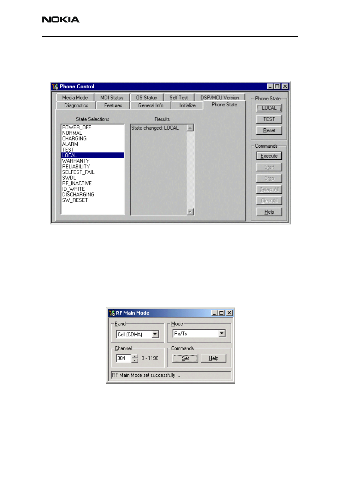
Use the following steps to set up the phone for Tx troubleshooting in Phoenix.
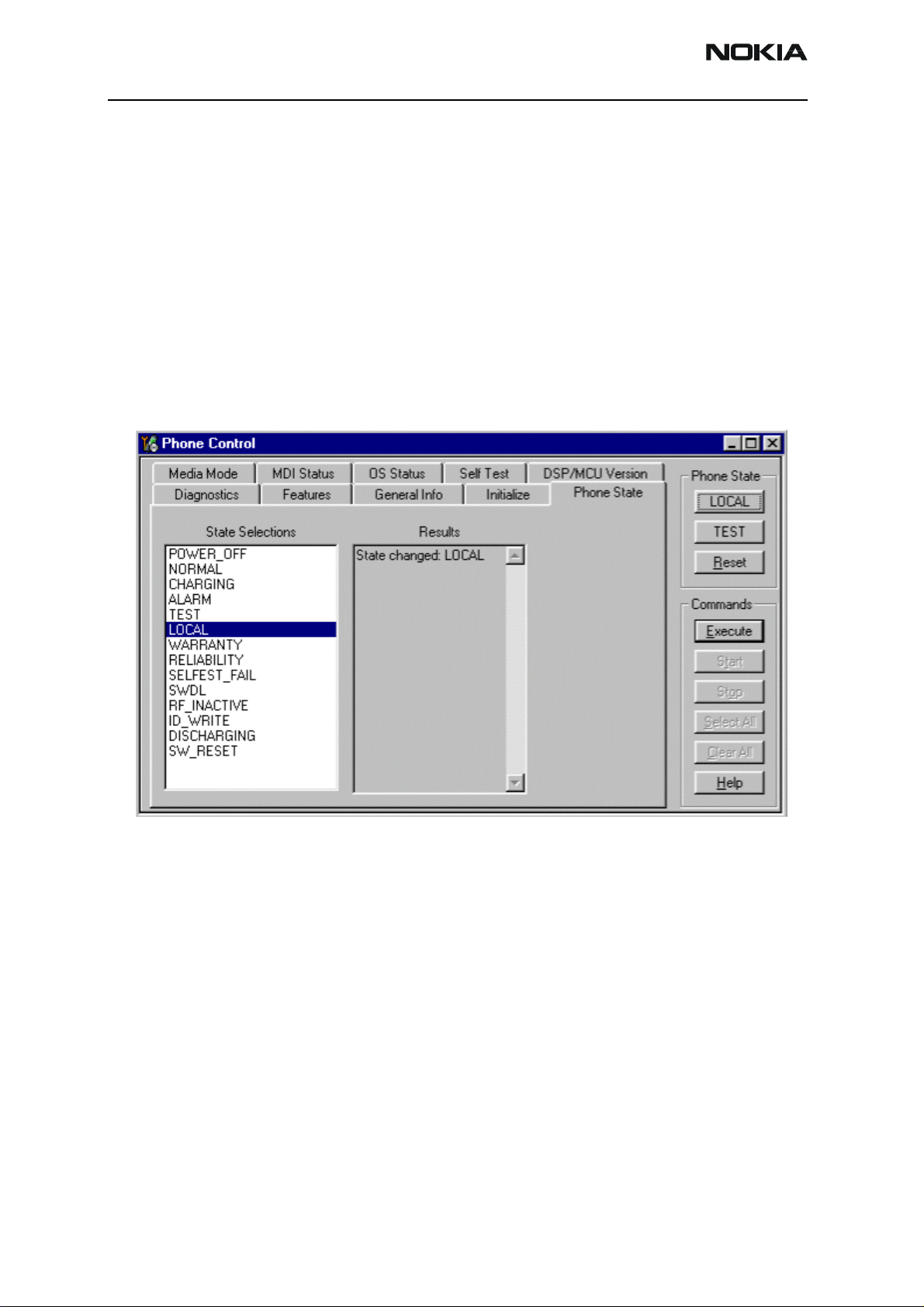
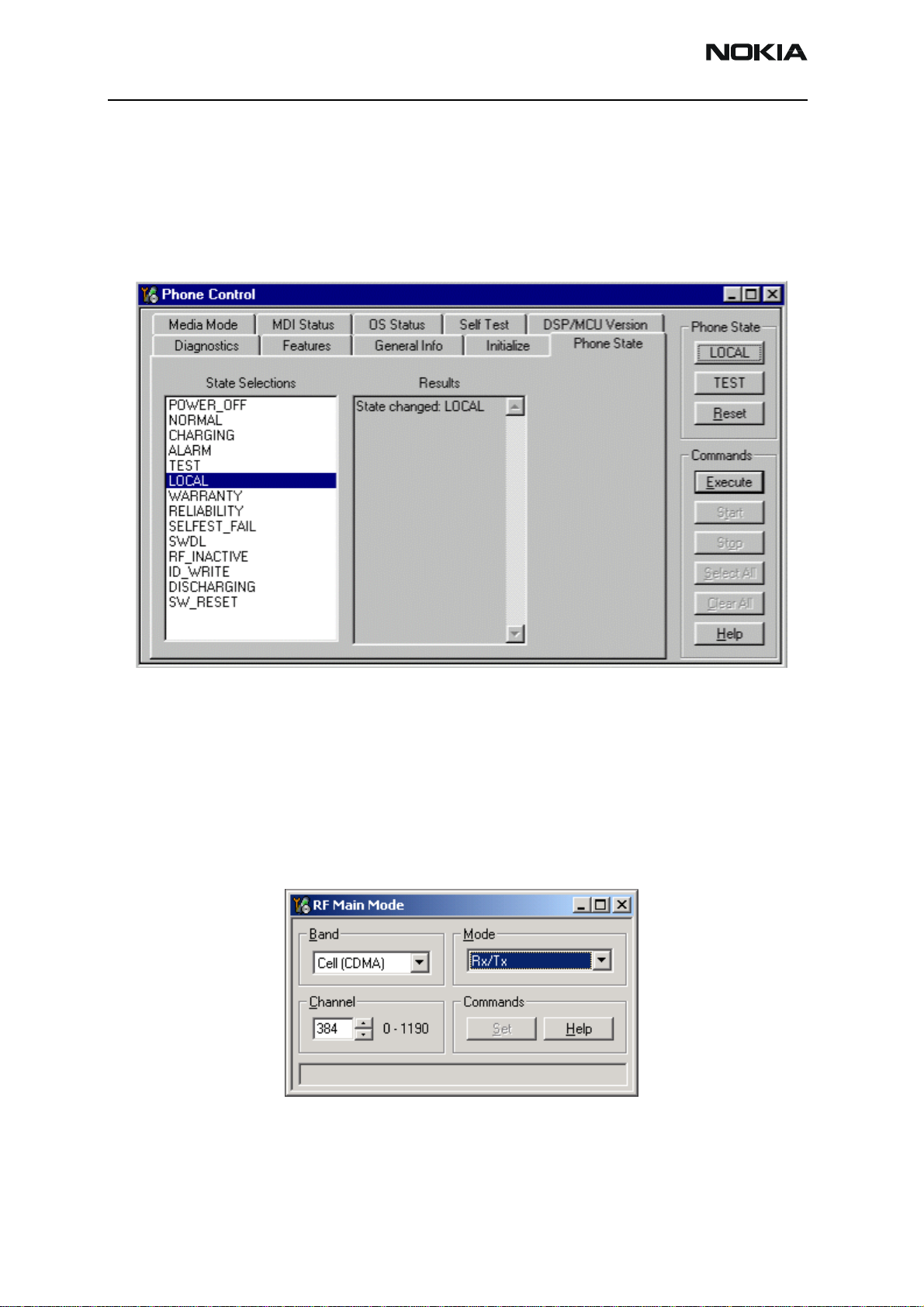
1. Open the Phone Control dialog box.
Figure 3: Phone Control dialog box for Tx troubleshooting
2. Click the LOCAL button in the Phone State area to put the phone into Local
Mode.
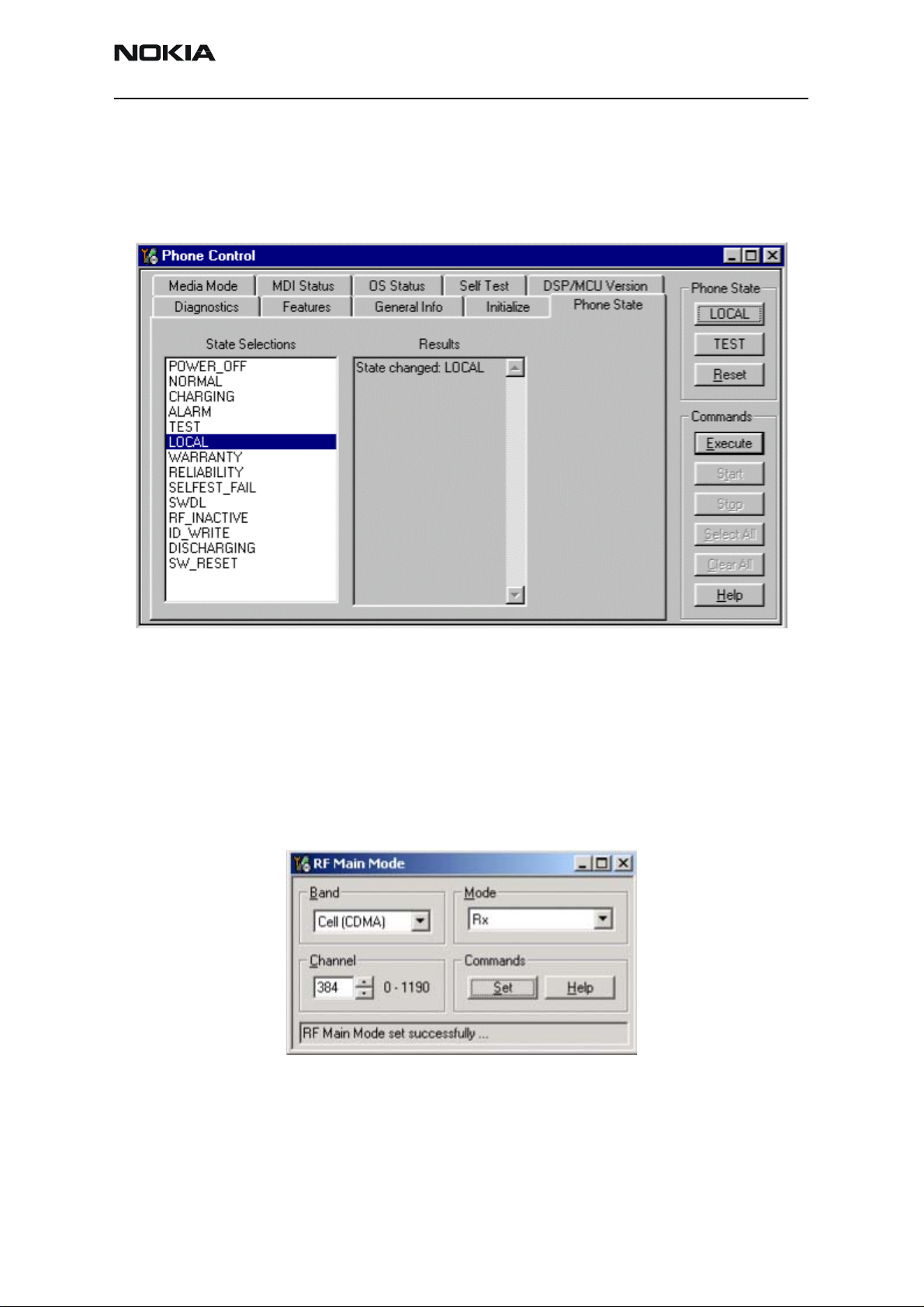
3. Select the following values on the RF Main Mode dialog box:
• Band = Cell (CDMA)
• Channel = 384
• Mode = Rx/Tx
Figure 4: RF Main Mode dialog box for Tx troubleshooting
4. Click Set.
Note: Be sure that the “RF Main Mode set successfully...” message appears in the status bar.
Issue 1 07/2004 ©2004 Nokia Corporation Company Confidential Page 7
Page 8
2112 (RH-57)
Troubleshooting - RF Nokia Customer Care
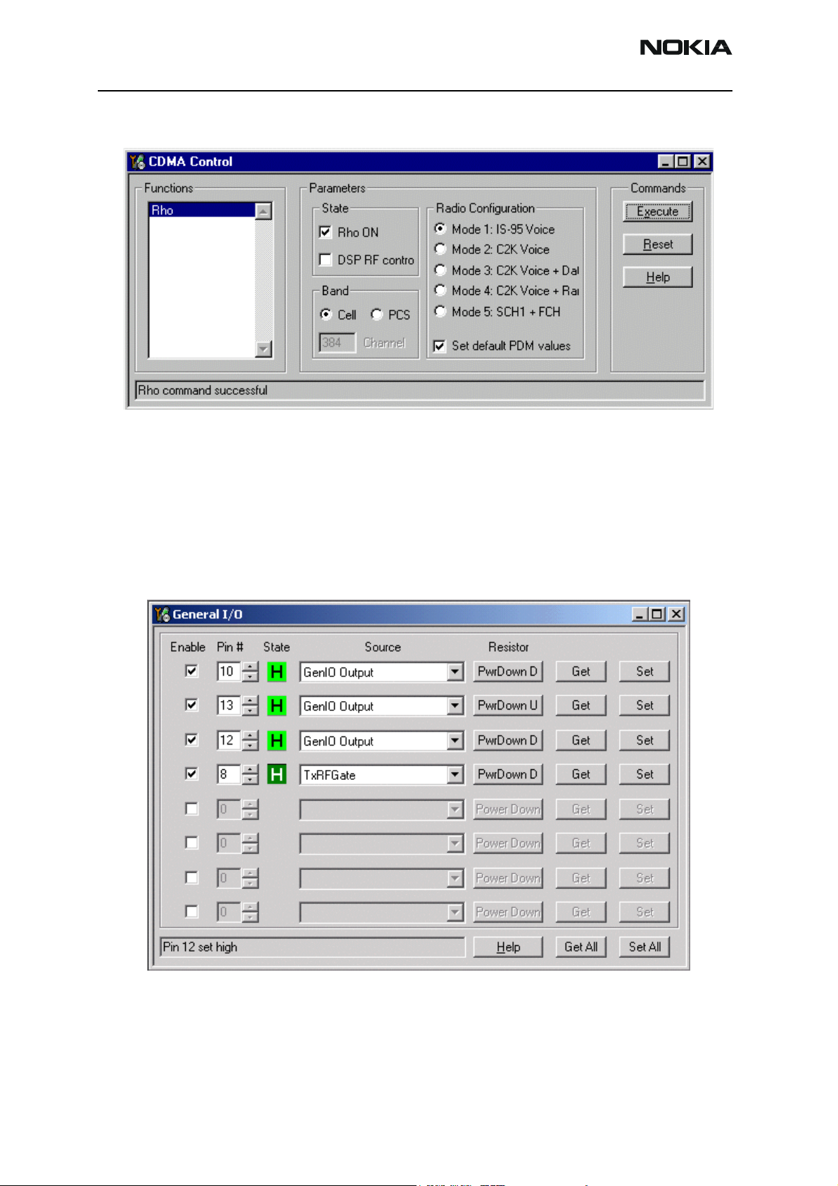
5. Select the Rho ON check box on the CDMA Control dialog box.
Figure 5: CDMA Control dialog box for Tx troubleshooting
6. Click Execute.
7. At this point you should be able to measure Tx Pout at the RF connector. The cell
band Tx Pout =0 to 2 dBm. If you do not see these values, set the AGC PDM for
25 dBm and probe the Tx path to figure out where in the path the fault occurs.
8. Open the General I/O dialog box to set the PA gain state.
9. Enter 10, 13, 12, and 8 in the PIN # fields.
Figure 6: General I/O dialog box for Tx troubleshooting
10. Select the boxes in the Enable column for each pin.
11. Cl i ck t h e Get All button.
Page 8 ©2004 Nokia Corporation Company Confidential Issue 1 07/2004
Page 9
2112 (RH-57)
Nokia Customer Care Troubleshooting - RF
12. Ensure that all of the pins have a value of H in the State column. (Click the L
values to change them to H values.)
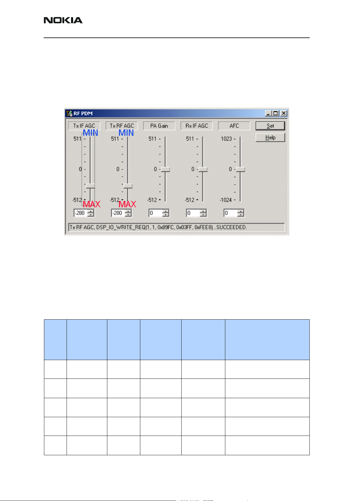
13. Adjust the following PDM field values on the RF PDM dialog box:
• Tx IF AGC = -280
• Tx RF AGC = -280
Figure 7: RF PDM dialog box for Tx troubleshooting
14. Ensure that the Phone Tx Pout = +25dBm and the current = 770-860mA.
Cell Transmitter Path
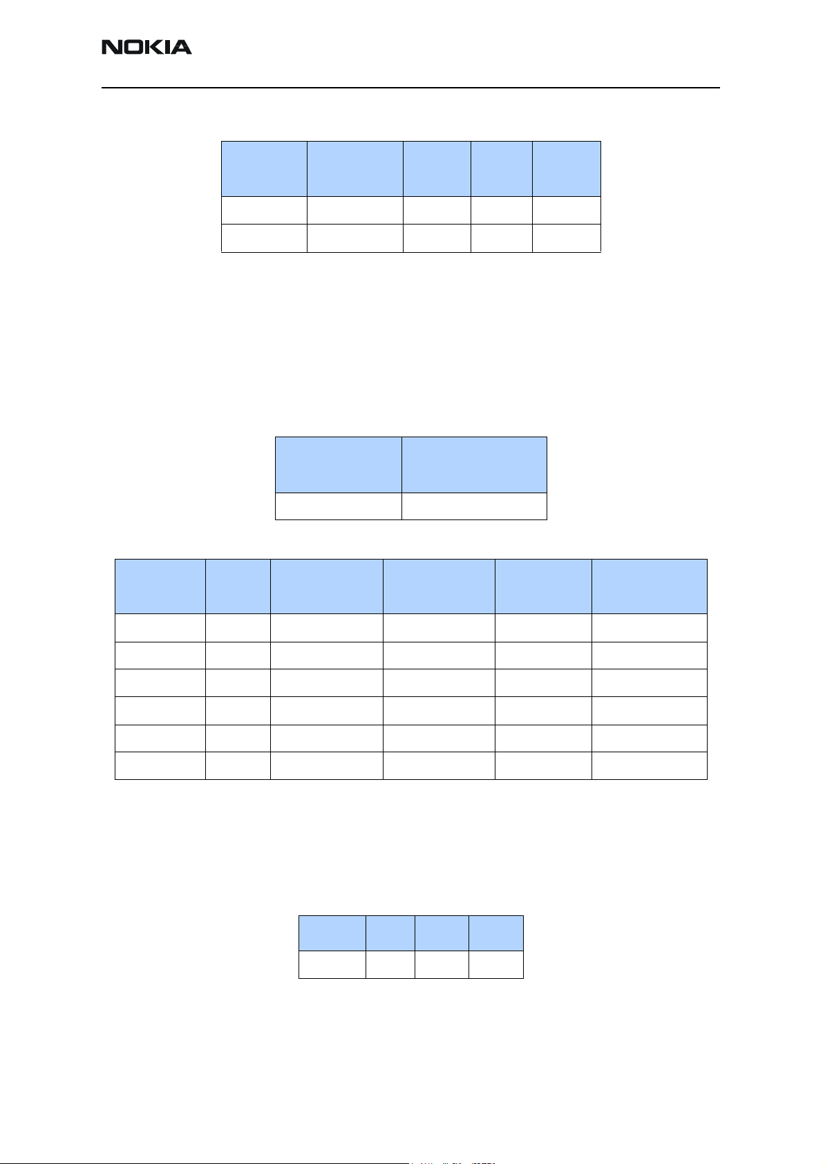
Table 1 indicates the test points (see Figure 8) to probe when troubleshooting the cell
transmitter path. It is recommended that you follow the steps in order. An HP high
frequency probe was used to make the frequency and output power measurements
Table 1: Cell Transmitter Test Points
Typical
Test
Point
Part* Function
Value/
Frequency
HP85024A
T1 Z601 pin1 Jedi-Out -43dBm/
836.52MHz
T2 Z601 pin 3 PA-In -25dBm/
836.52MHz
T3 N803 pin 8 PA-Out 5.0dBm/
836.52MHz
Typical
Value
Frequency
Prod Probe
-13.2dBm/
836.52MHz
-15.4dBm/
836.52MHz
18.3dBm/
836.52MHz
Comments
Output of Jedi Driver, Input to Tx
SAW Filter
Output of Tx SAW, Input to PA
Output of PA, Input to Isolator
T4 Z803T Iso-Out 2.2dBm/
836.52MHz
T5 C603L IF-Out -29dBm/
228.6MHz
10.3dBm/
836.52MHz
-24dBm/
228.6MHz
Output of Isolator, Input to
Duplexer
Tx IF Probing Point at IF Filter
Issue 1 07/2004 ©2004 Nokia Corporation Company Confidential Page 9
Page 10
2112 (RH-57)
Troubleshooting - RF Nokia Customer Care
Table 1: Cell Transmitter Test Points (Continued)
Typical
Test
Point
Part* Function
Value/
Frequency
HP85024A
T6 C638T, C654T,
C633R,
C635R,
C603LR
T7 C655R VR7 2.7V dc UHF PLL Supply from UEM
T8 C636L, C624T,
L609B, C612L,
C630B, L607B
T9 C605R, C606R VAGC-Tx 0.2 to 1.8V dc Tx AGC Control Voltage from
T10 C658R, C600T VIO-Tx 1.8V dc Supply for Digital circuits from
T11 C805B, C810T,
C816R
VR5 2.7V dc VHF VCO/PLL, IQ modulator
VR2 2.7V dc Mixer, driver, and IF supply from
VBAT 3.6V dc Battery Voltage
Typical
Value
Frequency
Prod Probe
Comments
supply from UEM
UEM
UPP.
0.2V = Max Gain
1.8V = Min Gain
UEM
(Nominal Voltage 3.6V dc)
T12 C802L, C813L VPA 3.6V dc
(High Gain)
T13 C814R VG 1.8V dc
(Enable)
* The R, L, T, and B values at the end of the part names indicate the Right, Left, Top, and Bottom side
of the part respectively in Figure 8 and Figure 9.
Main PA Supply Voltage from
PMIC. Lgain=0.8V,
Mgain=-1.25V, Hgain=Vbat
PA Gate Voltage (Enable/Disable)
Disable=0V
Page 10 ©2004 Nokia Corporation Company Confidential Issue 1 07/2004
Page 11
2112 (RH-57)
Nokia Customer Care Troubleshooting - RF
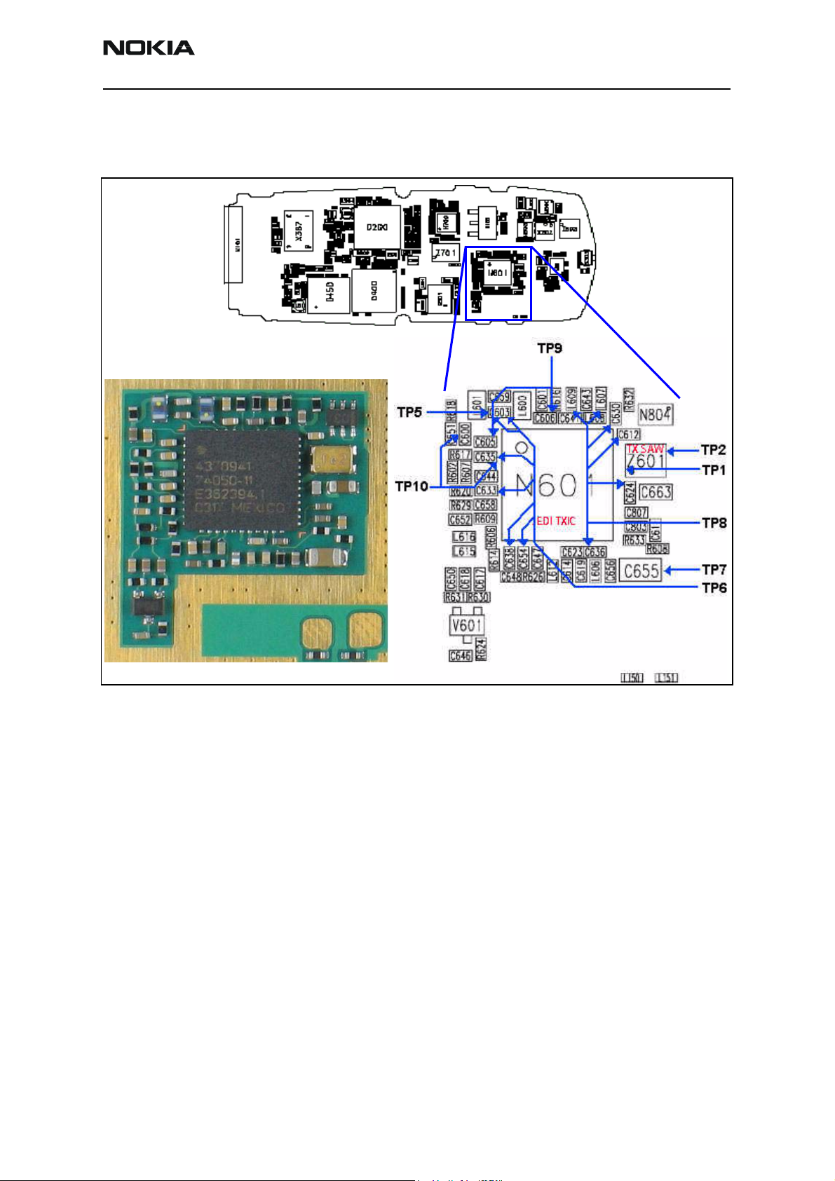
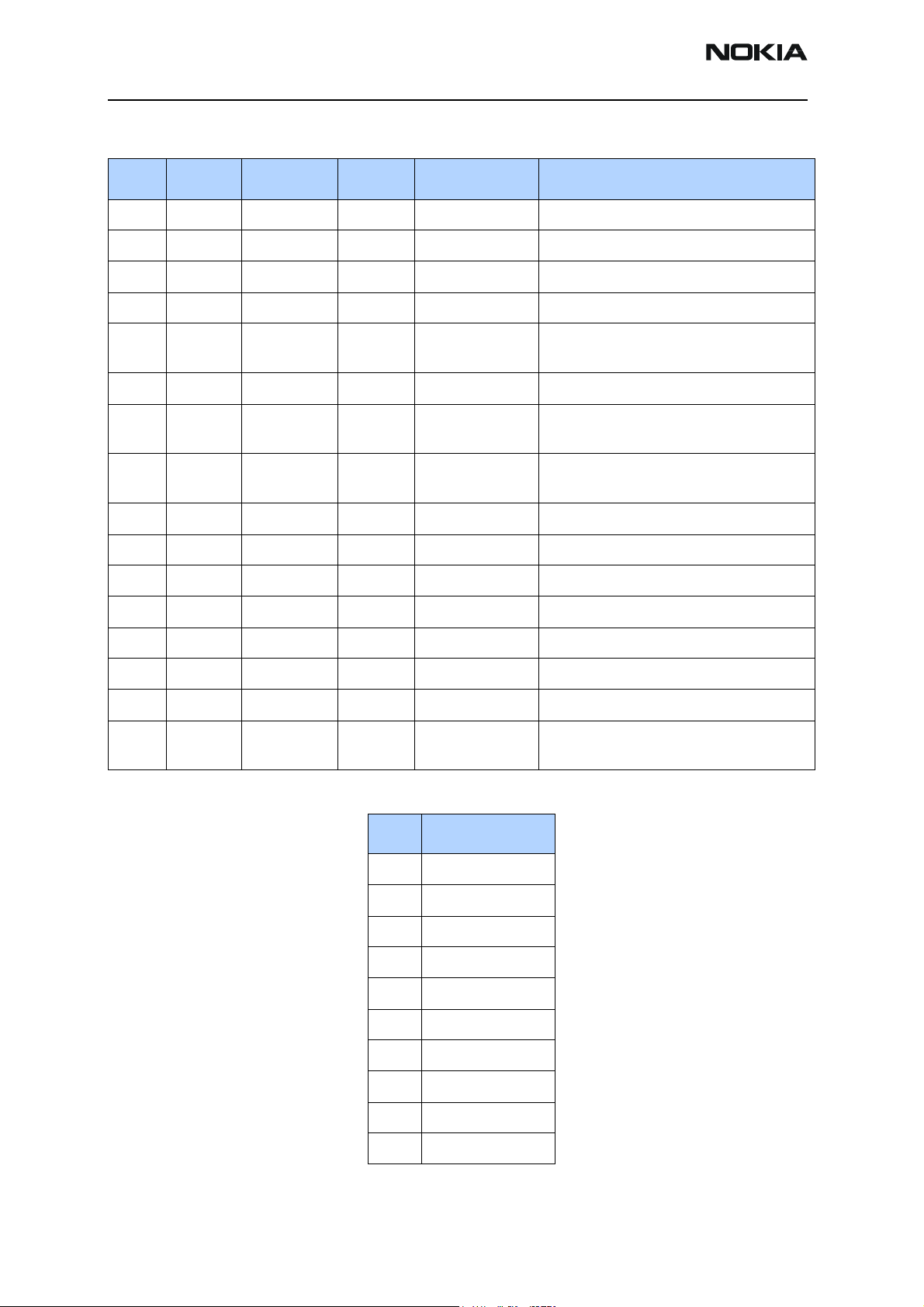
Figure 8 shows each test point for the Jedi TXIC section from Table 1, “Cell Transmitter
Test Points,” on page 9. Always attach a 20 dB pad (11881-60001) when probing with an
HP85024A high frequency probe.
Figure 8: (Top) PWB. (Bottom left) A zoomed view of the testing points on the Jedi TXIC section.
(Bottom right) A zoomed view of the Jedi TXIC section with part numbers.
Issue 1 07/2004 ©2004 Nokia Corporation Company Confidential Page 11
Page 12
2112 (RH-57)
Troubleshooting - RF Nokia Customer Care
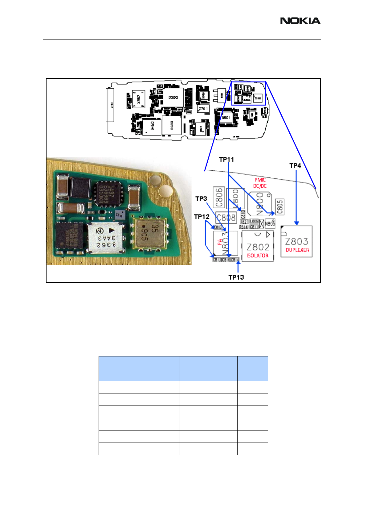
Figure 9 shows each testing point for the PA section from Table 1, “Cell Transmitter Test
Points,” on page 9. Always attach a 20 dB pad (11881-60001) when probing with an
HP85024A high frequency probe.
Figure 9: (Top) PWB. (Bottom left) A zoomed view of the testing points on the PA section.
Tx AGC Tuning
Tx power versus IF/RF PDM can be verified against FlaLi specification limits. Make sure
that the PA is set in high gain mode (GenIO bits 10, 13, and 12 are set to H).
(Bottom right) A zoomed view of the PA section with part numbers.
Table 2: Tx AGC Tuning Steps
Tx Tuning
AGC Step
Tx AGC (0) 308 -46 -55 -37
Tx AGC (1) 130 -24 -34 -14
Tx AGC (2) 85 -15 -25 -6
Tx AGC (3) 51 -4.5 -14 5
Tx AGC (4) 19 2.5 -7 12
Tx AGC (5) -5 6 -3 15
Tx AGC
PDM Value
Target
Power
Low
Limit
High
Limit
Page 12 ©2004 Nokia Corporation Company Confidential Issue 1 07/2004
Page 13
2112 (RH-57)
Nokia Customer Care Troubleshooting - RF
Table 2: Tx AGC Tuning Steps (Continued)
*Not an actual FlaLi tuning PDM. The PDM produces approximately 25dBm at the antenna
connector.
Cell Power Amplifier
The power amplifier (PA) has the DC/DC converter (PMIC device), which controls the
transmitter. The following tables show the circuits that have an effect on the transmitter
path and how to troubleshoot them.
Tx Tuning
AGC Step
Tx AGC (6) -94 15 6 24
Tx AGC (7)* -280* 25 21 27
Tx AGC
PDM Value
Table 3: PA Power and Gain Measurements
Power Amp
Input Test Point
pin3-Z601 left-R814
Table 4: PA Power and Gain Specifications
Target
Power
Low
Limit
Power Amp
Output Test Point
High
Limit
Mode Name
Gain mode 0 V0 up to 6 23.8 0.75- 0.88 C806
Gain mode 1 V1 6 to 11 25.2 1.125- 1.375 C806
Gain mode 3 V2 Not used Not used 2 - 2.5 C806
Gain mode 2 Bypass 11 up 29 3 - 4 C806
Gain mode 0 V0 up to 6 23.8 0.75- 0.88 C806
Gain mode 1 V1 6 to 11 25.2 1.125- 1.375 C806
*Not an actual FlaLi tuning PDM. PDM to produce approximately 25dBm at antenna connector.
Power Output
Range
Nominal Gain Vcc Range Vcc Test Point
Cell PMIC
The following tables show the PMIC troubleshooting information.
Table 5: PMIC Setup
Mode Tx Rx Band
Local On On CELL
Issue 1 07/2004 ©2004 Nokia Corporation Company Confidential Page 13
Page 14
2112 (RH-57)
Troubleshooting - RF Nokia Customer Care
Table 6: PMIC Measurements
Pin Label Test Point Units Depends On Comments
1 EP Pin 1 1.8 UPP IC enable = GenIO 10
2 M0 Pin 2 1.8 UPP Control 0 = GenIO 12
3 M1 Pin 3 1.8 UPP Control 1 = GenIO 13
4NC NC NC NC NC
5 FB Pin 5 0.75 - 4 M0, M1 See PA worksheet. Output to flyback
inductor.
6 FB Pin 6 0.75 - 4 M0, M1 Shares PWB pad with pin 5
7 BYPVout bottom-
C808
8 VDD right-L810 VBATT VBATT Digital DC supply, shared with pin 12,
9 VSS GND GND GND Digital GND, shared gnd with pin 13
10 NC NC NC NC NC
11 Vbgap NC NC NC Bandgap voltage output
12 VDD right-L810 VBATT VBATT Digital DC supply
13 Vss GND GND GND Digital GND, shared gnd with pin 9
14 Vsw right-L810 VBATT VBATT Switcher supply
15 Vsw right-L810 VBATT VBATT Switcher supply
16 Gsw GND GND GND Switcher GND, does not share with pin 9
0.75 - 4 M0, M1 PMIC bypass output used at
Pout > 12 dBm
14, and 15
and pin 13
Table 7: Good Phone PMIC Resistances
Pin Resistance
160k
275k
380k
41.59M
51.6M
62M
72M
82M
90.1
10 100
Page 14 ©2004 Nokia Corporation Company Confidential Issue 1 07/2004
Page 15
2112 (RH-57)
Nokia Customer Care Troubleshooting - RF
Table 7: Good Phone PMIC Resistances (Continued)
Pin Resistance
11 11 5k
12 60k
13 0.2
14 1.3M
15 1.18M
16 0.1
Cell IF/RF AGC and PA Control
Table 8, “Cell CDMA Channel 384 (Skyworks PA),” on page 16 illustrates the PDM values
and their typical values for the IF AGC, RF AGC Jedi Pout, gain steps, and the PA VCC
levels. This table also shows the typical power output at the RF connector.
Issue 1 07/2004 ©2004 Nokia Corporation Company Confidential Page 15
Page 16

2112 (RH-57)
Troubleshooting - RF Nokia Customer Care
Table 8: Cell CDMA Channel 384 (Skyworks PA)
Tx RF AGC Tx IF AGC Jedi Po PA Gain Step PA Vcc
Conn RF
PDM
Typical
Value
Test
Point
PDM
Typical
Value
Test
Point
Typical
Value
Test
Point
Gen IO 12 Gen IO 13
Typical
Value
Test
Point
PA
Gain
Pout
-290 0.45 Bottom
C606
-196 0.59 -196 0.59 -2 H H 3.61 28 20
-95 0.75 -95 0.75 -9.2 H H 3.67 28 13.2
-95 0.75 -95 0.75 -9.2 H L 1.2 26 11
-48 0.83 -48 0.83 -13 H L 1.2 25.8 7
-48 0.83 -48 0.83 -13 L L 0.82 24.5 6
17 0.93 17 0.93 -19 L L 0.82 0
80 1.04 80 1.04 -29 L L 0.82 -10
120 1.11 120 1.11 -39 L L 0.82 -20
168 1.19 168 1.19 -49 L L 0.82 -30
249 1.32 249 1.32 -59 L L 0.82 -40
324 1.49 324 1.49 -69 L L 0.82 -50
-290 0.45 Top
C605
3pin 1
Z601
H H 3.47 C806 DM 25
Page 16 ©2004 Nokia Corporation Company Confidential Issue 1 07/2004
Page 17

2112 (RH-57)
Nokia Customer Care Troubleshooting - RF
Cell Power Detector
The following tables illustrate the measurements required for troubleshooting the cell
power detector.
Table 9: Cell Power Setup
Mode Tx Rx Band Chnn Rho
Local On On CELL 384 On
Input Chnn Tx Freq Rx Freq
384 836.52 881.52
Table 10: Cell Power Measurements: Cell, Channel 384
Tx ADC
RF/IF
pdm
324 L L -50 -86.3 Right
142 L L -25 -63 2 235
17 L L 0 -41 1.998 235
-48 L L 6 -30 1.967 250
-48 H L 7 -29 1.957 268
-95 H L 11 -26 1.93 286
-95 H H 13.2 -23.5 1.9 435
-146 H H 17 -21.5 1.86 486
-178 H H 19 -19 1.812 550
PA Gain
Step
GIO 12GIO
13
Conn
RF Pout
Pout at
Detector
Power Detector Comments
Test
Point
R814
Det
Out
2Left
Test
Point
C807
mA
235 CELL band and
Det=Detector
Po=Power
detector
coupling is about
22 dB
-214 H H 21 -17 1.745 630
-252 H H 23 -15 1.667 730
-290 H H 25 -12 1.547 860
-316 H H 26 -11.5 1.485 950
-328 H H 26.5 -11 1.44 1000
-351 H H 27.5 -10 1.36 1095
none dBm dBm/
30kHz
VDC dBm only refers
to total power
measured
Issue 1 07/2004 ©2004 Nokia Corporation Company Confidential Page 17
Page 18
2112 (RH-57)
Troubleshooting - RF Nokia Customer Care
Table 11: Detector Reference and DC Supply
label Test Point Typical Value
Det Ref left-C803 2
Det Supply bottom-C257 2.8
VDC
Page 18 ©2004 Nokia Corporation Company Confidential Issue 1 07/2004
Page 19
2112 (RH-57)
Nokia Customer Care Troubleshooting - RF
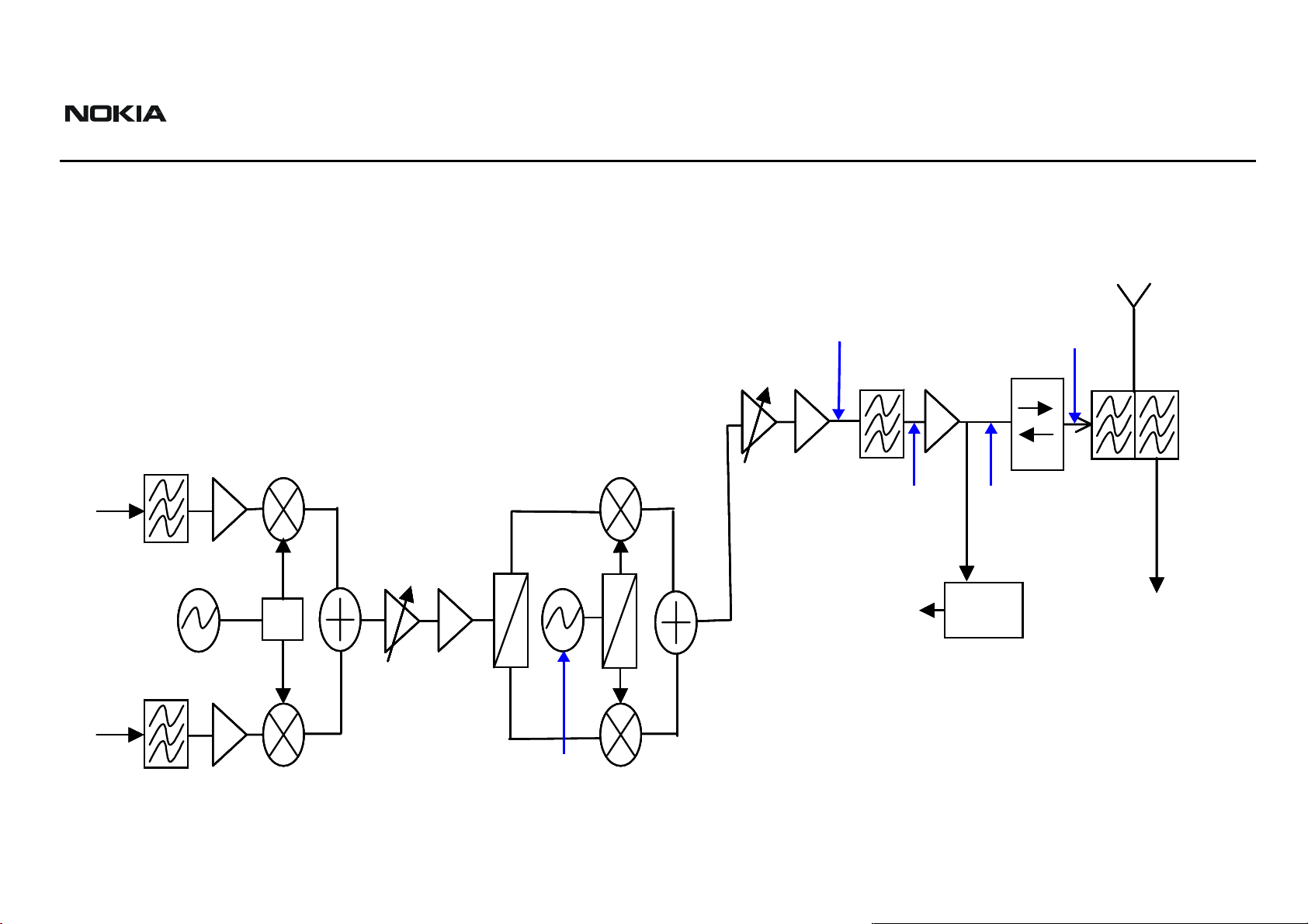
Tx System Block Diagram
Note: See the Schematics chapter for a 2112 transmitter schematic.
Antenna
Antenna
Antenna
Antenna
I
I
I
From
From
From
From
Baseband
Baseband
Baseband
Baseband
Q
Q
Q
BB I LPF
457.2MHz
VHF LO
VHF LO
VHF LO
VHF LO
÷2/÷4
÷2/÷4
÷2/÷4
÷2/÷4
90º
90º
90º
90º
IQ Modulator
0º
0º
0º
IF VGA
(IF AGC PDM)
UHF LO
UHF LO
UHF LO
0º
0º
0º
0º0º
90º
90º
90º
1052.61-107757MHz
Upconverter
0º
0º
0º
0º
0º
0º
0º0º
90º
90º
90º
90º
90º
90º
90º
90º
RF VGA
(RF AGC PDM)
TP1
Bandpass
Tx SAW
To Baseband
To Baseband
To Baseband
PWR Amplifier
TP2 TP3
Power
Power
Power
Power
Detector
Detector
Detector
Detector
Isolator
Isolator
Isolator
TP4
Cell RX
Cell RX
Cell RX
Cell RX
Duplexer
Duplexer
Duplexer
Duplexer
Figure 10: Tx system block diagram
Issue 1 07/2004 ©2004 Nokia Corporation Company Confidential Page 19
Page 20
2112 (RH-57)
Troubleshooting - RF Nokia Customer Care
Receiver Troubleshooting
Rx IF
Use Phoenix to perform the following steps for troubleshooting the receiver. Together
with the VCO frequency and level verification, this test should be the first test for a nonworking receiver. This test verifies the entire receiver chain, from input connector to
baseband output.
1. Inject a CW signal 881.82MHz or 881.22MHz (CH-384 offset by 300KHz) at a
fixed –75dBm power level. If you do not have a signal generator, use the CALL
BOX in AMPS mode on Channel 374 or 394 (10 channels away from
channel 384).
2. Open the Phone Control dialog box.
Figure 11: Phone Control dialog box for Rx IF troubleshooting
3. Click the LOCAL button in the Phone State area to put the phone into Local
Mode.
4. Select the following values on the RF Main Mode dialog box:
• Band = Cell (CDMA)
• Channel = 384
• Mode = Rx
Page 20 ©2004 Nokia Corporation Company Confidential Issue 1 07/2004
Page 21

2112 (RH-57)
Nokia Customer Care Troubleshooting - RF
Figure 12: RF Main Mode dialog box for Rx IF troubleshooting
5. Click Set.
Note: Be sure that the “RF Main Mode set successfully...” message appears in the status bar.
6. Use a spectrum analyzer to test TP3 (I+,I-, Q+, Q-). Set the S.A to 300KHz center
frequency, 200KHz SPAN, and +10dBm reference level. The spectrum analyzer
should read –8dBm without any settings to the PDM.
7. Use the following CDMA Generator Code Domain Setup table to configure the
CDMA generator code domain.
Table 12: CDMA Generator Code Domain Setup
Channel Power Walsh Code
Pilot -7dB 0
Paging -12dB 1
Traffic -15.6dB 10
Sync -16dB 32
Table 13 shows the steps for Rx IF troubleshooting. See Figure 13 on page 23 for an
illustration of the corresponding test points.
Step # Part Function
Table 13: Rx IF Troubleshooting
Typical
Value/
Frequency
HP85024A
Typical
Value
Frequency
Prod Probe
Comments
TP1 L702R IF-IN +1.3 dBm/
183.6MHz
TP2 L701L/R SAW Out -16 dBm/
183.6MHz
-12/-27 dBm
183.6MHz
-35/-50 dBm
183.6MHz
I.F Input to Z701 (I.F filter).
NOT 50 ohm
Differential outputs of Z701.
NOT 50 ohm
Issue 1 07/2004 ©2004 Nokia Corporation Company Confidential Page 21
Page 22

2112 (RH-57)
Troubleshooting - RF Nokia Customer Care
Table 13: Rx IF Troubleshooting (Continued)
Typical
Step # Part Function
Value/
Frequency
HP85024A
TP3 I+, I-, Q+, Q- I/Q outputs
of Yoda N700
TP4 C728T 19.2MHz In +6.5 dBm
TP5 C711T 19.2MHz Out +4 dBm
TP6 L708R (L708R
for Prod
Probe)
TP7 C731T VREF 1.35Vdc System reference voltage
VHF VCO +1.0 dBm
300KHz tone
for input:
881.22MHz
19.2MHz
19.2MHz
367.2MHz
Typical
Value
Frequency
Prod Probe
-69/-84 dBm
300KHz
-22 dBm
19.2MHz
-25 dBm
19.2MHz
-61 dBm
367.2MHz
Comments
Baseband differential outputs of the IF IC (N700). To
test: set the input to 881.22
or 881.82MHz/-75dBm to
get a 300KHz tone when
receiver is on channel 384
(881.52MHz)
Sine wave input to N700
from VCTCXO.
Square wave output of N700
to baseband.
Rx VHF VCO - Fixed at
367.2MHz (Be careful not to
load the circuit with the
probe.)
1.35Vdc from UEM.
TP8 R702L
(C703R)
TP9 R703T (R701L,
R715T)
TP10 C734B VR3 2.7Vdc VCTCXO buffer supply from
TP11 C712R, C744R VR6 2.7Vdc Main supply to N700, from
TP12 C710T, C704B VIO 1.8Vdc Digital circuits supply from
* The R, L, T, and B values at the end of the part numbers indicate the Right, Left, Top, and Bottom
side of the part respectively in Figure 13.
RX_IF_AGC 0.2 to 1.8 Vdc AGC control Voltage. 0.2V =
Max Gain, 1.8V = Minimum
Gain
VR7 2.7Vdc VHF VCO Supply from UEM
UEM.
UEM.
UEM.
Page 22 ©2004 Nokia Corporation Company Confidential Issue 1 07/2004
Page 23

2112 (RH-57)
Nokia Customer Care Troubleshooting - RF
Figure 13 shows each test point as listed in Table 13.
Figure 13: (Top) PWB. (Bottom left) A zoomed view of the testing points on the Rx IF section.
(Bottom right) A zoomed view of the Rx IF section with part numbers.
Issue 1 07/2004 ©2004 Nokia Corporation Company Confidential Page 23
Page 24

2112 (RH-57)
Troubleshooting - RF Nokia Customer Care
Figure 14 shows an alternate part orientation. Notice that Pin 1 is rotated 180 degrees
compared to the first filter as shown in Figure 13 on page 23. All test points and values
are the same.
Figure 14: Alternate part orientation with pin 1 rotated 180 degrees
Page 24 ©2004 Nokia Corporation Company Confidential Issue 1 07/2004
Page 25
2112 (RH-57)
Nokia Customer Care Troubleshooting - RF
Switching the Gain
Use the following steps if the receiver is not working properly and you need to switch the
Rx gain state.
1. Open the Phone Control dialog box.
Figure 15: Phone Control dialog box for switching the Rx gain state
2. Click the LOCAL button in the Phone State area to put the phone into Local
Mode.
3. Select the following values on the RF Main Mode dialog box:
• Band = Cell (CDMA)
• Channel = 384
• Mode = Rx
Figure 16: RF Main Mode dialog box for switching the Rx gain state
4. Click Set.
Note: Be sure that the “RF Main Mode set successfully...” message appears in the status bar.
Issue 1 07/2004 ©2004 Nokia Corporation Company Confidential Page 25
Page 26

2112 (RH-57)
Troubleshooting - RF Nokia Customer Care
5. Connect a signal generator in CW mode (881.52MHz, -25dBm) to the RF
connector. If you do not have a generator, use the Call Box Amps Mode RF
Generator, Channel 384, -25dBm and set the FM modulation to 100Hz, deviation
400Hz.
6. To switch the Rx gain states, open the RF Register R/W dialog box. Two gain
states (Hi and Lo) are available in the receiver.
High gain state
Figure 17: RF Register R/W dialog box for switching Rx gain states
7. Select the appropriate gain states from Register #6. The following values apply:
• Bit 0=1, means a Hi gain state.
• Bit 0=0, means a Lo gain state.
Page 26 ©2004 Nokia Corporation Company Confidential Issue 1 07/2004
Page 27

2112 (RH-57)
Nokia Customer Care Troubleshooting - RF
Rx RF
The following Rx RF Troubleshooting table indicates the test points to probe when
troubleshooting the Rx RF. It is recommended that you follow the steps in order. See
Figure 18 on page 28 for an illustration of the test points.
Table 14: Rx RF Troubleshooting
Typical
Step # Part Function
Value/
Frequency
HP85024A
R1 L802R (Top
side of the
PWB)
R2 L906L LNA-In -35dBm/
R3 C903L LNA-Out -13/-31dBm
R4 Z901-R-Bot-
tom, N901Pin16
R5 C906R Mixer-out -5/-21dBm
R6 C912B/R914R IF Output to
R7 R912B/R911L L.O Input to
RF-IN -25dBm/
881.52MHz
881.52MHz
881.52MHz
RF Filter Output
Mixer-In
N700
N901
-18/-35dBm
881.52MHz
183.6 MHz
+1.5/-15dBm
183.6MHz
-2.5dBm
1065.12MHz
Typical
Value
Frequency
Prod Probe
-42dBm
881.52MHz
-42dBm
881.52MHz
-29/-45dBm
881.52MHz
-30/-45dBm
881.52MHz
-23/-38dBm
183.6MHz
-12/-29dBm
183.6MHz
-18dBm
1065.12MHz
Comments
Input Connector reference
level
Test Duplexer insertion Loss
(Without DC Block)
Test LNA gain ~ 13dB
Test RF Filter Insertion loss
(Without DC Block)
Test Output on Downconverter on N901
Test Alfred output to Yoda
IF-IC (N700)
Test VCO output to Alfred
(N901) Levels are for Channel 384
R8 R9056T,
L909L, L901T,
R910B
R9 R902B Rx-SW1 H.G = 2.7V
* The R, L, T, and B values at the end of the part names indicate the Right, Left, Top, and Bottom side
of the part respectively in Figure 18.
VR4 2.7V dc Power supply to Alfred
L.G = 0V
(N901)
LNA gain control, on the
Alfred side, High Gain >
2.5V dc
Issue 1 07/2004 ©2004 Nokia Corporation Company Confidential Page 27
Page 28

2112 (RH-57)
Troubleshooting - RF Nokia Customer Care
Antennae
Connector
(top side)
R1
Figure 18: (Top left) PWB. (Top right) The antenna connector on the opposite side of the PWB, (Bottom left)
A zoomed view of the testing points on the Rx RF section. (Bottom right) A zoomed view of the Rx RF section
with part numbers.
Page 28 ©2004 Nokia Corporation Company Confidential Issue 1 07/2004
Page 29

2112 (RH-57)
Nokia Customer Care Troubleshooting - RF
Rx AGC (Cell mode)
The following Rx RF AGC PDM vs. AGC Voltage table shows the Rx RF AGC PDM vs. AGC
voltages in local mode on channel 384.
Table 15: Rx RF AGC PDM vs. AGC Voltage
PDM Typical Value Test Point
-512 0.08 right R702
-400 0.260
-300 0.436
-200 0.597
-100 0.753
00.913
100 1.076
200 1.24
300 1.403
350 1.494
400 1.570
500 1.740
511 1.761
UNITS VDC
Table 16: Rx AGC vs. RF Pin for CELL Band
Conn RF Pin CELL RF AGC Comments
-25 1.492
-35 1.298
-45 1.159 In Normal mode, the phone will adjust RF RX AGC
-55 1.019 Rx power is coming in, the I and Q will be about 0.5Vpp and 1.3V
-65 0.861
-75 0.705 Approximately 1pdm per 1mV
-85 0.530
-92 0.425
-95 0.633 Note the reduced delta because the LNA is switched on
-100 0.594
-105 0.524
Issue 1 07/2004 ©2004 Nokia Corporation Company Confidential Page 29
Page 30

2112 (RH-57)
Troubleshooting - RF Nokia Customer Care
Table 16: Rx AGC vs. RF Pin for CELL Band (Continued)
Conn RF Pin CELL RF AGC Comments
-107 0.470
UNITS VDC
Page 30 ©2004 Nokia Corporation Company Confidential Issue 1 07/2004
Page 31

2112 (RH-57)
÷
Nokia Customer Care Troubleshooting - RF
Receiver Block Diagram
Note: See the Schematics chapter for a 2112 receiver schematic.
LNA SW Control
I/Q Down
Converter
CDMA
BB Filter
TX
Antenna
Duplexer
LNA
CELL
SAW
Loop Filter
RFA
UHF VCO
1052.61-1077.57
UHF Synthsizer
JEDI
IFA
IF SAW
VCTCXO
VGA
CDMA
BB Filters
2
BB AMP
To BB
BB AMP
VHF PLL
367.2 MHz
Bias and Control
Reference Clock
To Base-Band
AFC
Figure 19: Receiver block diagram
Issue 1 07/2004 ©2004 Nokia Corporation Company Confidential Page 31
Page 32

2112 (RH-57)
Troubleshooting - RF Nokia Customer Care
Synthesizer Troubleshooting
Faulty synthesizers can cause both Rx and Tx failures during tuning, in addition to the
VCTCXO tuning. The following synthesizers are incorporated into the 2112 (RH-57):
• UHF (cell) PLL inside Jedi IC (N601)
• Tx VHF (457.2MHz) with PLL in Jedi IC in Cell Mode
• Tx VHF (527.2MHz) with PLL in Jedi IC in PCS Mode
• Rx VHF (367.2MHz) with PLL in Yoda IC
Synthesizer Setup
Use the following steps to set up the phone for Tx troubleshooting in Phoenix.
1. Open the Phone Control dialog box.
Figure 20: Phone Control dialog box for Tx troubleshooting
2. Click the LOCAL button in the Phone State area to put the phone into Local
Mode.
3. Use the following settings for the Band, Channel, and Mode fields on the RF
Main Mode dialog box:
• UHF: Use the Rx/Tx mode and channel 384 in Cell band. This allows you to
check power in both the Rx and Tx circuits.
• Rx VHF: Use the Rx mode. One band is enough.
• Tx VHF: Use the Rx/Tx mode in Cell band.
Page 32 ©2004 Nokia Corporation Company Confidential Issue 1 07/2004
Page 33

2112 (RH-57)
Nokia Customer Care Troubleshooting - RF
Figure 21: RF Main Mode dialog box for synthesizer troubleshooting
4. Click Set.
Note: Be sure that the “RF Main Mode set successfully...” message appears in the status bar.
5. Read register templates Jedi(0) bits 10 and 11 for the UHF and Tx VHF lock
condition on the RF Register R/W dialog box.
Figure 22: RF Register R/W dialog box for synthesizer setup
6. Read register templates Yoda(0) bit 11 for the RX VHF lock condition.
VCTCXO Tuning
The VCTCXO can be manually tuned to verify failed tuned phones, or to verify if a phone
cannot make a call. This can be done with the phone in Local Mode and generating a CW
signal. The frequency accuracy of the VCTCXO can be measured using an HP8960 callbox
Issue 1 07/2004 ©2004 Nokia Corporation Company Confidential Page 33
Page 34
2112 (RH-57)
Troubleshooting - RF Nokia Customer Care
in AMPS mode, an HP4406 Tx tester, or a spectrum analyzer (preferably using a lab
system 10MHz source as equipment reference). Replace the VCTCXO if the VCTCXO AFC
DAC value does not meet the tuning requirements after tuning.
Use the following steps to manually tune the VCTCXO:
1. Open the Phone Control dialog box.
Figure 23: Phone Control dialog box for VCTCXO troubleshooting
2. Click the LOCAL button in the Phone State area to put the phone into Local
Mode.
3. Select the following values on the RF Main Mode dialog box:
• Band = Cell (CDMA)
• Channel = 384
• Mode = Rx/Tx
Figure 24: RF Main Mode dialog box for VCTCXO troubleshooting
4. Do not use CDMA control to turn on Rho.
5. Open the BB General I/O dialog box to set the CW signal.
Page 34 ©2004 Nokia Corporation Company Confidential Issue 1 07/2004
Page 35

2112 (RH-57)
Nokia Customer Care Troubleshooting - RF
6. Type 10, 13, 12, and 8 in the fields in the PIN # column.
Figure 25: General I/O dialog box for VCTCXO tuning
7. Click the Get All button.
8. Change the value for Pin 8 in the Source column to GenIO Output.
9. Ensure that all of the pins have a value of H in the State column. (Click the L
values to change them to H values.)
10. The next step depends on the type of measurement equipment you are using:
• HP4406 or a spectrum analyzer: Set the center frequency to 836.52MHz and
the span to 2MHz. Also, establish a marker at 836.52MHz.
• HP8960: Set the callbox state to AMPS, and set the channel to 384. Use the
Frequency Accuracy measurement to center the VCTCXO.
Issue 1 07/2004 ©2004 Nokia Corporation Company Confidential Page 35
Page 36

2112 (RH-57)
Troubleshooting - RF Nokia Customer Care
11. Adjust the AFC value to center the VCTCXO on the RF PDM dialog box. The
tuning range is approximately +/- 10kHz.
Figure 26: Manually adjusting the AFC to center VCTCXO
12. Adjust the AFC value so that the output signal is within +/- 100Hz. If you are
using an HP4406 or a spectrum analyzer, narrow the span to 1kHz or less.
Page 36 ©2004 Nokia Corporation Company Confidential Issue 1 07/2004
Page 37

2112 (RH-57)
Nokia Customer Care Troubleshooting - RF
VCTCXO Reference Clock
Figure 27 shows the 19.2 MHz VCTCXO reference clock.
Figure 27: (Top) PWB. (Bottom left) A zoomed view of the testing points on the 19.2 MHz VCTCXO reference
clock. (Bottom right) A zoomed view of the 19.2 MHz VCTCXO reference clock with part numbers.
Issue 1 07/2004 ©2004 Nokia Corporation Company Confidential Page 37
Page 38

2112 (RH-57)
Troubleshooting - RF Nokia Customer Care
Synthesizer Block Diagram
Note: See the Schematics chapter for an 2112 (RH-57) synthesizer schematic.
CELL:457.2MHz
CELL:457.2MHz
JEDI
JEDI
367.2MHz
367.2MHz
VHF
VHF
counter
counter
Yoda
Yoda
19.2MHz
19.2MHz
VCTCXO
VCTCXO
19.2MHz to
19.2MHz to
UPP
UPP
VHF
VHF
counter
counter
UHF
UHF
counter
counter
CELLl Band UHF VCO
CELLl Band UHF VCO
Figure 28: Synthesizer block diagram
Page 38 ©2004 Nokia Corporation Company Confidential Issue 1 07/2004
Page 39
2112 (RH-57)
Nokia Customer Care Troubleshooting - RF
UHF Synthesizer
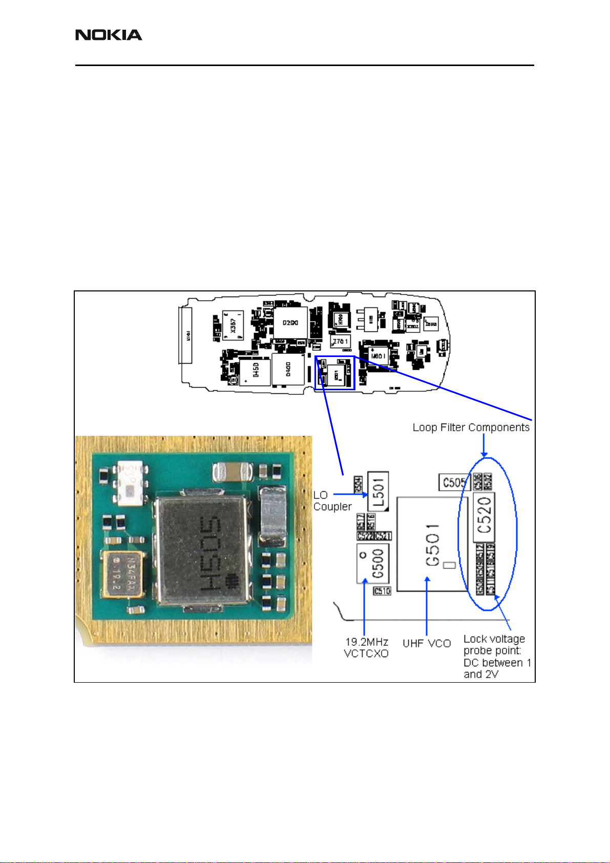
Following are possible causes for an incorrect UHF frequency:
• Orientation of Jedi
• Power supplies to Jedi PLL (N601) are missing or low (VR7)
• Loop filter components are missing or incorrectly installed
• Matching components to Jedi TxLO/PLL input are missing or incorrectly installed
• 19.2MHz reference clock is missing or low
• Programming is incorrect
• Component failure (VCO or PLL portion of Jedi)
Figure 29 and Figure 30 show the UHF synthesizer layout.
Figure 29: (Top) PWB. (Bottom left) A zoomed view of the testing points on the UHF synthesizer layout.
(Bottom right) A zoomed view of the UHF synthesizer layout with part numbers.
Issue 1 07/2004 ©2004 Nokia Corporation Company Confidential Page 39
Page 40

2112 (RH-57)
Troubleshooting - RF Nokia Customer Care
Figure 30: (Top) PWB. (Bottom left) A zoomed view of the Jedi LO/PLL input match components on the UHF
synthesizer layout (Bottom right) A zoomed view of the Jedi LO/PLL input match components UHF synthesizer
layout with part numbers.
Rx VHF
Following are possible causes for an incorrect Rx VHF frequency:
• Power supplies to the PLL portion of Yoda IC (N700) are missing or low (VR7)
• Loop filter or resonator components are missing or incorrectly installed
• 19.2MHz reference clock is missing or low (C510)
• Programming is incorrect
Note: See the Schematics chapter for an Rx VHF schematic.
Page 40 ©2004 Nokia Corporation Company Confidential Issue 1 07/2004
Page 41

2112 (RH-57)
Nokia Customer Care Troubleshooting - RF
Figure 31 shows the layout for the Rx VHF.
Figure 31: (Top) PWB. (Bottom left) A zoomed view of the testing points on the Rx VHF section.
(Bottom right) A zoomed view of the Rx VHF section with part numbers.
Tx VHF
Following are possible causes for an incorrect Tx VHF frequency:
• Power supplies to the PLL portion of Jedi IC (N601) missing or low (VR5)
• Loop filter or resonator components are missing or incorrectly installed
• 19.2MHz reference clock is missing or low (C510)
• Programming is incorrect
• Component failure (Jedi IC)
Note: See the Schematics chapter for a Tx VHF schematic.
Issue 1 07/2004 ©2004 Nokia Corporation Company Confidential Page 41
Page 42

2112 (RH-57)
Troubleshooting - RF Nokia Customer Care
Figure 32 shows the layout for the Tx VHF.
Figure 32: (Top) PWB. (Bottom left) A zoomed view of the testing points on the Tx VHF section.
(Bottom right) A zoomed view of the Tx VHF section with part numbers.
Page 42 ©2004 Nokia Corporation Company Confidential Issue 1 07/2004
Page 43

2112 (RH-57)
Nokia Customer Care Troubleshooting - RF
Tuning Descriptions
Tuning Title Description Troubleshooting
Tx Detector This is one of the phone's self-tests
which gives either a pass or fail result
only. The phone transmits at several
power levels and checks the ADC value
of the power detector. The ADC value is
measured first for a set of AGC values,
then each AGC value is changed one at
a time to make sure that the ADC
changes as each AGC is changed individually.
Cell PA Temp This is one of the phone's self tunings,
which reads the ADC voltage of a thermistor R821, and checks to make sure
the phone is at room temperature. The
reason for this is that a phone should
not be tuned while it is hot or cold.
Check the AGC voltages and components of
the associated PDMs. For problems with the
IF or RF AGC, also check Jedi and supporting
components. For PA AGC problems, also
check the PA and supporting components. If
all of the above cases fail, troubleshoot the
Tx chain. If all the output powers are passing, then perhaps the test is failing because
the ADC voltage is wrong (which at this
point we cannot read, so we are measuring
the actual output power). If the voltages are
wrong, then check the power detector at
N805, C803, C807, and also Jedi. If the voltages are correct and it still fails, check the
UEM (D200).
If the phone was recently transmitting in
Cell band at full power for an extended
period of time, it is probably hot for that
reason. Let it cool down for a few minutes,
then try again. If it still fails, there may
either be a short on the board or else a
problem with the PA Temp circuitry. To
check PA Temp circuitry, check R821 and
D200. If a short is suspected, check the cell
PA first. If an infrared camera is available,
this is one of the easiest methods to detect
a short.
Cell Rx DC Offset I
(or Q)
Tx Start-up Current This test turns on the transmitter and
Tx Start-up Amplitude This test turns on the transmitter and
This is one of the phone's self tunings,
which measures and adjusts the cell
band CDMA receiver DC offsets until
they are within the limits.
measures current of the whole phone,
which can detect some assembly errors.
checks for the presence of a Tx signal
with an amplitude within a specified
range. A wide range is allowed since the
transmitter is not yet tuned.
Check Yoda (N701) and supporting components.
If current is very high, there may be a short
circuit on the phone caused by a solder
bridge, a failed component that is internally
shorted, a component placed with the
wrong rotation which shorts two nodes that
should not be, or some other reason. A visual inspection can find solder bridges or
wrong component rotations. A failed component can be found by functional tests of
the phone's sub-blocks.
Check proper placement, rotation, and soldering of the components in the Tx chain.
Check for the presence of LO tones. Check
for the presence of a Tx signal at each point
in the Tx chain.
Issue 1 07/2004 ©2004 Nokia Corporation Company Confidential Page 43
Page 44
2112 (RH-57)
Troubleshooting - RF Nokia Customer Care
Tuning Title Description Troubleshooting
VCTCXO Frequency The purpose of this tuning is to deter-
mine what the AFC DAC value needs to
be in order to center the VCTCXO frequency. The transmitter is turned on and
no Tx baseband modulation is provided.
The carrier is then centered in frequency.
This is done to the carrier after it has
been mixed up to 836.52MHz, since it's
easier to measure the tolerance of 1ppm
at 836.52MHz than it is at 19.2MHz.
Additionally, the tone at 836.52MHz can
be measured without taking the phone
apart.
1) If there is no tone, probe pin 3 of G501
for a tone at 19.2 MHz. If this is not present,
check power supplies, particularly ensure
2.7v on VCTCXO Vcc pin, pin 4 of G501. Also
check the control pin, pin 1 of G501, for a
voltage between 0.4 and 2.7v. If the voltages are correct, and soldering of all G501
terminals is correct, replace G501. If 19.2
MHz tone is present but tone at
836.52 MHz is not, troubleshoot cell Tx
chain.
2) If the carrier is present but the PDM
needed to center it is outside of the +/- 150
range, or if it cannot be centered, there is a
hardware problem.
3) In the following procedure, performing
frequency centering on the RF carrier at
836.52MHz will detect frequency errors due
to the VCTCXO and supporting hardware,
which will account for the majority of the
problems, but will not detect frequency
errors due to the hardware that mixes the
VCTCXO tone at 19.2MHz up to 836.52MHz.
In order to troubleshoot this hardware, frequency centering should be performed on
the 19.2MHz tone to +/- 19.2Hz on pin 3 of
G501 using a frequency counter, then the
VHF and UHF LOs should be checked.
Because this will be time-consuming and
will probably only account for a small percentage of the failures, it is not recommended unless the situation justifies the
time spent. The VHF LO is inside the Jedi IC
(N601) and troubleshooting of the cell UHF
LO is required.
4) If the carrier can be centered but the
PDM is out of range, check the control voltage on pin 1 of G501. If it is 2.2v, (and pin 4
is at 2.7v, and pin 2 at 0v), then the VCTCXO
(G501) is working correctly but the circuit
that delivers the control voltage is not.
Check soldering of all G501 terminals, also
check R510, R511, C503, and D200. If the
control voltage on pin 1 of G501 is not 2.2v,
but the carrier is centered, then there is a
problem with the VCTCXO G501. If there is
2.7v on pin 4 and the soldering is correct,
then replace G501.
Page 44 ©2004 Nokia Corporation Company Confidential Issue 1 07/2004
Page 45

2112 (RH-57)
Nokia Customer Care Troubleshooting - RF
Tuning Title Description Troubleshooting
5) If the carrier cannot be centered, check
to see if you can adjust to 2.2v on pin 1 of
G501. If you can, within the PDM range of
+/- 150, then the circuitry that delivers the
voltage is working correctly, and the
VCTCXO has a problem. Troubleshoot it as
described in the previous section. If you
cannot adjust to 2.2v within the accepted
range, then the AFC circuitry has a problem.
Troubleshoot it as described in the previous
section.
6) If there is a fault with both the AFC circuitry and the VCTCXO, then several combinations of the previously described
conditions are possible. Start by ensuring
2.2v on pin 1 of G501 using a PDM within
the range +/- 150, then center the tone.
PA Gain Cell Po(0)Po(3)
Tx AGC This tuning characterizes the AGC curve
These tunings model the cell PA gain
curve by setting the PA AGC PDM to
several values and measuring output
power. First, the Tx PA AGC and the Tx
RF AGC are set to (approximately) their
maximum used values (not the maximum possible values, but the maximum
of the range over which they are used).
Then the Tx IF AGC is set so that the
transmit power on the antenna connector is approximately +11dBm (this power
is reported in the next tuning). Then, six
PDM values are written to the PA AGC
and the output power is measured for
each. These values are reported in this
tuning. The software then performs
curve fitting to interpolate between the
measured data points.
by entering PDM values to the RF AGC
and measuring the output power.
If the power readings are low, check the
AGC voltages. You can also probe on the PA
input to find out if the power level is low
going into the PA, or if the power level is
correct going into the PA but the PA gain is
too low. If the power level going into the PA
is too low, probe the Tx chain at all the
other points prior to the PA listed in the
table to see where the gain is lacking. When
that point is identified, check the soldering
of all related components, and replace components until the fault is found. If the
power on the PA input is not low and the PA
AGC voltage is correct, similarly probe the
power at all points after the PA to find the
fault, being extremely careful not to short
the probing point to ground because this
will instantly destroy the PA. Visually check
soldering first, and probe on PA output as a
last resort.
Check Jedi (N601). Also check D400, which
generates the PDM signals. Check AGC PDM
voltages. Troubleshoot the rest of the cell
transmitter if needed.
Issue 1 07/2004 ©2004 Nokia Corporation Company Confidential Page 45
Page 46

2112 (RH-57)
Troubleshooting - RF Nokia Customer Care
Tuning Title Description Troubleshooting
Tx Gain Comp This tuning ensures that the value of
TxdBCtr correctly corresponds to the
absolute Tx output power. On the mid
channel, with TxdBCtr set to a specified
value, G_Offset is adjusted so that the
output power is -8dBm, and that value
of G-Offset is recorded (which is an
absolute value) in the next tuning. The
output power in dBm is recorded in this
tuning.
TN G_Offset See description of previous tuning. This
step reports G_Offset.
Tx Limiting Cell This tuning provides an upper limit on
the transmit power while in Cell IS95
mode. The reason for this is to ensure
that the phone never goes above the
maximum transmit power level. After
this is done on the mid channel, the
channel is changed to each of the other
channels, and detector offset is
reported.
Set the phone to local mode and program it
to Cellular CDMA Rx/Tx mode on channel
384, using the Main Mode window. Using
the Phoenix RF Tuning window, choose
mode = RF Tuning, and choose this test.
Adjust G_Offset in the "Values” dialog box
line until the Tx output power (measured on
the RF connector with a spectrum analyzer)
is equal to -8.0dBm +/- 0.5dB. Use the
G_Offset limit range as a guide to which
values to enter.
If G_Offset is not within the limits, troubleshoot the Cell Tx.
If the maximum cannot be reached, either a
component in the transmitter has too much
loss, or not enough gain. Troubleshoot the
transmitter, with the phone set to the same
channel as the failed channel. Once this is
done on the center channel, change to each
of the other channels, and record the power.
Do not adjust G_Offset on the other channels, just record the power. It should be
within the limits listed in the tuning results
file.
Channel Cell Power
Low 1013 22.86-23.06
LowMid 125 23.61-23.81
MidLow 225 24.16-24.36
Mid 384 25.03-25.23
MidHigh 558 24.83-25.03
HighMid 750 24.60-24.80
High 777 24.57-24.77
Rx IF AGC Rx dB Ctr This tuning calibrates the Rx IF AGC
curve. The tuner injects three known
signal power levels into the phone's
receiver, and for each one the phone's
AGC algorithms, adjusts the RX_IF_AGC
to get the same amplitude at the output
of Yoda, although different amplitudes
are going in. From these three points,
curve fitting is used to interpolate
between measurement points.
LNA Gain This tuning records RxdBCtr (which is
automatically adjusted to produce the
same amplitude on the receiver output
no matter what the input is) for the
receiver with the LNA in high gain mode,
and again with the LNA in low gain
mode.
While injecting a signal into the receiver,
check the values of RX_IF_AGC PDM value
and, if needed, voltage. RSSI should be
within +/- 2 dB of the actual power in dBm
on the RF connector. The AGC will try to
keep the same amplitude on Yoda output;
therefore, if the AGC value is larger than
normal, then the AGC is compensating for
loss in the chain prior to the variable gain
amplifier.
Check Alfred and supporting components.
Page 46 ©2004 Nokia Corporation Company Confidential Issue 1 07/2004
 Loading...