

DATA SHEET
NPN SILICON RF TWIN T RANSISTOR
NPN SILICON EPITAXIAL TWIN TRANSISTOR
(WITH BUILT-IN 2
FLAT-LEAD 6-PIN THIN -TYPE ULTRA SUPER MINIMOLD
FEATURES
• Low noise and high gain
• Operable at low voltage
re
• Small feedback capacitance: C
• Flat-lead 6-pin thin-type ultra super minimold package
• Built-in 2 transistors (2 × 2SC5010)
ORDERING INFORMATION
= 0.4 pF TYP.
2SC5010)
××××
µµµµ
PA826TC
Part Number Package Quantity Supplying Form
µ
PA826TC Loose products
µ
PA826TC-T1
Remark
ABSOLUTE MAXIMUM RATINGS (TA = +25
Parameter Symbol Ratings Unit
Collector to Base Voltage V
Collector to Emitter Voltage V
Emitter to Base Voltage V
Collector Current I
Total Power Dissipation
Junction Temperature T
Storage Temperature T
Flat-lead 6-pin
thin-type ultra
super minimold
To order evaluation samples, please contact your local NEC sales office. (Part number for sample order:
PA826TC. Unit sample quantity is 50 pcs).
µ
P
(50 pcs)
Taping products
(3 kp/reel)
CBO
CEO
EBO
C
Note
T
180 in 1 element
230 in 2 elements
j
stg
−
Embossed tape 8 mm wide.
Pin 6 (Q1 Base), Pin 5 (Q2 Emitter), Pin 4 (Q2 Base) face to perforation
side of the tape.
C)
°°°°
9V
6V
2V
30 mA
mW
150 °C
65 to 150 °C
Mounted on 1.08 cm
Note
The information in this document is subject to change without notice. Before using this document, please
confirm that this is the latest version.
Not all devices/types available in every country. Please check with local NEC representative for
availability and additional information.
Document No. P14553EJ1V0DS00 (1st edition)
Date Published November 1999 N CP(K)
Printed in Japan
2
× 1.0 mm glass epoxy substrate.
Caution Electro-static sensitive devices
1999©
ELECTRICAL CHARACTERISTICS (TA = +25 °C)
Parameter Symbol Conditions MIN. TYP. MAX. Unit
µµµµ
PA826TC
Collector Cutoff Current I
Emitter Cutoff Current I
DC Current Gain h
Gain Bandwidth Product f
Feedback Capacitance C
Insertion Power Gain |S
CBO
EBO
21e
VCB = 10 V, IE = 0
VEB = 1 V, IC = 0
FE
T
VCE = 3 V, IC = 7 mA
VCE = 3 V, IC = 7 mA, f = 1 GHz 10.0 12.0
VCB = 3 V, IE = 0, f = 1 MHz
re
2
|
VCE = 3 V, IC = 7 mA, f = 1 GHz 7.0 8.5
Note 1
Noise Figure NF VCE = 3 V, IC = 7 mA, f = 1 GHz
Notes 1.
Pulse Measurement: PW ≤ 350
Capacitance between collector and base measured with a capacitance meter (auto−balancing bridge
2.
s, Duty Cycle ≤ 2%
µ
method). Emitter should be connected to the guard pin of capacitance meter.
hFE CLASSIFICATION
Rank KB
Marking 83
hFE Value 75 to 150
Note 2
−−
−−
75
−
−
−
0.4 0.7 pF
1.5 2.5 dB
0.1
0.1
150
−
−
A
µ
A
µ
GHz
dB
2
Data Sheet P14553EJ1V0DS00
µµµµ
PA826TC
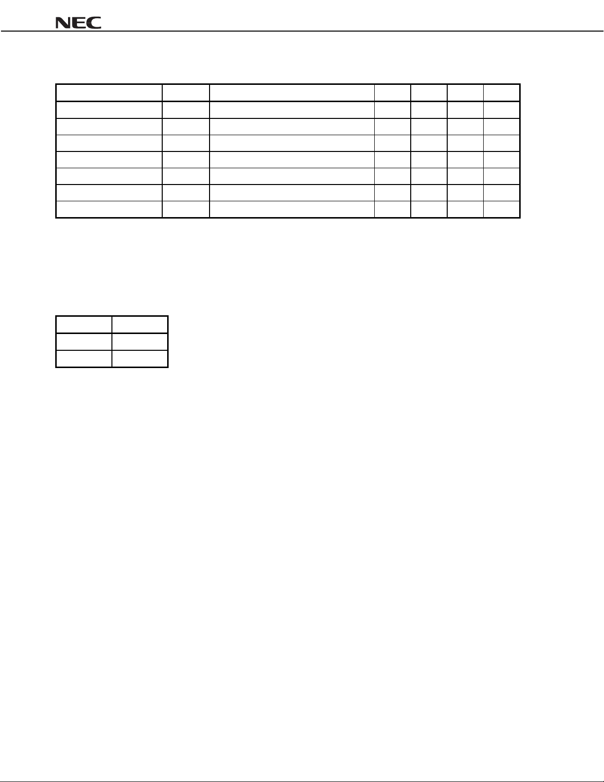
TYPICAL CHARACTERISTICS (TA = +25
TOTAL POWER DISSIPATION vs.
AMBIENT TEMPERATURE
230
200
180
100
Total Power Dissipation PT (mW)
20
16
12
Collector Current IC (mA)
0
8
4
0
2 Elements in total Free Air
Per
Element
0 50 100 150
Ambient Temperature TA (°C)
COLLECTOR CURRENT vs.
COLLECTOR TO EMITTER VOLTAGE
IB = 160 A
IB = 140 A
IB = 120 A
IB = 100 A
IB = 80 A
IB = 60 A
IB = 40 A
IB = 20 A
0123456
Collector to Emitter Voltage VCE (V)
C)
°°°°
COLLECTOR CURRENT vs.
DC BASE VOLTAGE
50
VCE = 3 V
40
30
20
10
Collector Current IC (mA)
0
0 0.5 1.0
DC Base Voltage VBE (V)
DC CURRENT GAIN vs.
COLLECTOR CURRENT
1 000
µ
µ
µ
µ
µ
µ
µ
µ
100
DC Current Gain hFE
10
0.1 1 10 100
Collector Current IC (mA)
VCE = 3 V
GAIN BANDWIDTH PRODUCT vs.
COLLECTOR CURRENT
18.00
VCE = 3 V
f = 2 GHz
16.00
14.00
12.00
10.00
Gain Bandwidth Product fT (GHz)
8.00
1 10 100
Collector Current IC (mA)
12.00
(dB)
2
10.00
8.00
6.00
4.00
Insertion Power Gain S21e
2.00
Data Sheet P14553EJ1V0DS00
INSERTION POWER GAIN vs.
COLLECTOR CURRENT
VCE = 3 V
f = 2 GHz
1 10 100
Collector Current IC (mA)
3
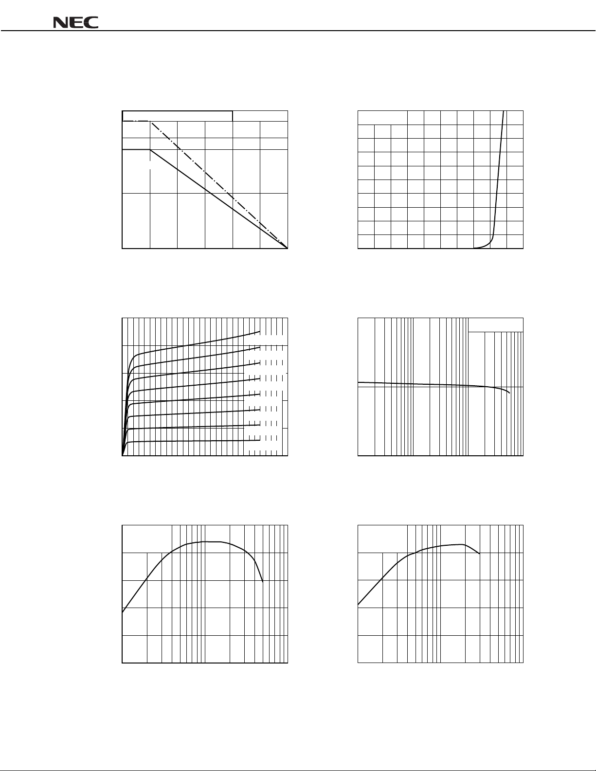
NOISE FIGURE vs. COLLECTOR CURRENT
10.00
VCE = 3 V
f = 2 GHz
8.00
6.00
4.00
0.400
(pF)
re
0.300
0.200
FEEDBACK CAPACITANCE vs.
COLLECTOR TO BASE VOLTAGE
f = 1 MHz
µµµµ
PA826TC
Noise Figure NF (dB)
2.00
0.00
1 10 100
Collector Current IC (mA)
INSERTION POWER GAIN vs. FREQUENCY
30.0
VCE = 3 V
C
= 10 mA
I
25.0
(dB)
2
21e
20.0
15.0
10.0
5.0
Insertion Power Gain S
0.0
0.1 1.0 10.0
Frequency f (GHz)
0.100
Feedback Capacitance C
0.000
1 10 100
Collector to Base Voltage VCB (V)
4
Data Sheet P14553EJ1V0DS00

µµµµ
PA826TC
S-PARAMETERS Q1
CE
= 3 V, IC = 1 mA
V
FREQUENCY S
GHz MAG.ANG.MAG.ANG.MAG.ANG.MAG.ANG.
11
21
S
12
S
S
22
0.1 0.962
0.2 0.939
0.3 0.925
0.4 0.900
0.5 0.887
0.6 0.841
0.7 0.809
0.8 0.774
0.9 0.737
1.0 0.695
1.1 0.656
1.2 0.622
1.3 0.591
1.4 0.557
1.5 0.528 176.8 2.491 11.1 0.178
1.6 0.501 164.3 2.414 1.0 0.185
1.7 0.477 151.6 2.333
1.8 0.453 139.1 2.267
1.9 0.434 126.6 2.196
2.0 0.416 114.2 2.120
2.1 0.400 100.9 2.060
2.2 0.389 88.4 1.988
2.3 0.381 75.3 1.930
2.4 0.372 62.9 1.866
2.5 0.364 50.9 1.801
2.6 0.369 39.1 1.753
2.7 0.371 27.4 1.706
2.8 0.374 16.2 1.662
2.9 0.380 5.3 1.622
3.0 0.387
14.0 3.900 166.5 0.031 34.7 1.012
−
25.6 3.769 154.0 0.044 70.0 0.986
−
38.2 3.657 142.4 0.058 61.6 0.980
−
51.3 3.558 130.1 0.075 48.7 0.965
−
63.0 3.505 118.5 0.089 39.6 0.941
−
75.3 3.365 106.7 0.105 30.7 0.918
−
88.2 3.262 94.8 0.115 20.4 0.889
−
100.0 3.176 83.8 0.127 10.5 0.865
−
111.6 3.064 72.8 0.140 3.2 0.838
−
123.9 2.954 61.9 0.144
−
135.9 2.843 51.6 0.155
−
147.4 2.760 41.1 0.162
−
159.8 2.660 30.8 0.170
−
171.5 2.579 21.0 0.175
−
8.7 0.186
−
18.1 0.191
−
27.3 0.196
−
37.0 0.196
−
46.1 0.197
−
55.7 0.199
−
64.5 0.197
−
73.7 0.200
−
82.2 0.200
−
90.6 0.203
−
99.1 0.202
−
107.7 0.204
−
115.8 0.203
5.7 1.575
−
−
124.6 0.207
−
6.4 0.806
−
15.5 0.775
−
23.4 0.753
−
30.9 0.726
−
38.4 0.705
−
46.0 0.679
−
53.6 0.655
−
61.2 0.635
−
68.4 0.613
−
75.6 0.594
−
82.6 0.573
−
89.9 0.557
−
95.5 0.535 176.8
−
102.9 0.515 169.2
−
108.7 0.494 161.7
−
115.5 0.478 154.7
−
119.5 0.468 147.9
−
126.2 0.465 140.3
−
132.3 0.456 131.9
−
138.6 0.445 124.1
−
144.4 0.438 115.8
−
VCE = 3 V, IC = 3 mA
FREQUENCY S
GHz MAG.ANG.MAG.ANG.MAG.ANG.MAG.ANG.
11
21
S
12
S
S
9.6
−
19.1
−
28.7
−
38.0
−
47.0
−
56.1
−
64.7
−
73.4
−
82.0
−
90.6
−
98.6
−
106.5
−
114.6
−
122.4
−
130.1
−
137.7
−
145.6
−
153.2
−
160.6
−
168.1
−
175.3
−
22
0.1 0.897
0.2 0.852
0.3 0.811
0.4 0.753
0.5 0.693
0.6 0.630
0.7 0.572
0.8 0.520
0.9 0.477
1.0 0.430
1.1 0.396
1.2 0.364
1.3 0.338 173.4 4.206 17.2 0.129
1.4 0.313 160.3 3.973 8.1 0.133
1.5 0.298 147.3 3.765
1.6 0.281 133.4 3.574
1.7 0.271 120.0 3.416
1.8 0.262 106.3 3.252
1.9 0.258 93.2 3.122
2.0 0.255 80.2 2.976
2.1 0.258 66.4 2.868
2.2 0.260 54.1 2.743
2.3 0.265 42.4 2.644
2.4 0.275 31.1 2.548
2.5 0.280 19.4 2.455
2.6 0.293 9.2 2.380
2.7 0.301
2.8 0.312
2.9 0.324
3.0 0.335
19.4 9.548 161.9 0.017 64.0 0.985
−
34.6 8.940 146.2 0.038 62.6 0.955
−
50.0 8.404 131.7 0.059 54.4 0.918
−
66.7 7.863 117.0 0.066 44.1 0.864
−
81.0 7.381 103.8 0.072 36.3 0.804
−
94.7 6.795 91.1 0.082 25.6 0.754
−
109.1 6.304 78.9 0.088 14.9 0.707
−
121.6 5.842 67.8 0.095 7.6 0.662
−
135.0 5.452 56.8 0.107 2.4 0.623
−
147.6 5.076 46.4 0.110
−
160.5 4.745 36.3 0.117
−
173.4 4.475 26.7 0.122
−
0.9 0.137
−
9.9 0.144
−
18.8 0.147
−
27.4 0.154
−
36.0 0.159
−
44.6 0.165
−
52.9 0.168
−
61.4 0.172
−
69.6 0.176
−
77.8 0.183
−
85.9 0.188
−
94.1 0.194
1.5 2.301
−
11.1 2.223
−
20.5 2.163
−
29.5 2.090
−
−
101.8 0.198
−
109.9 0.203
−
117.8 0.208
−
125.7 0.214
−
−
−
−
−
−
−
−
−
5.0 0.587
−
12.0 0.559
−
18.8 0.529
−
26.4 0.504
−
32.3 0.481
−
38.6 0.463
−
44.6 0.443
−
50.0 0.425
−
56.2 0.406
−
63.2 0.393
−
68.0 0.376
−
75.3 0.361
−
81.5 0.348 173.0
−
87.4 0.334 165.3
−
93.4 0.321 157.6
−
99.6 0.308 149.7
−
104.8 0.298 141.6
−
110.8 0.285 133.8
−
118.0 0.274 125.6
−
123.6 0.266 116.6
−
129.9 0.257 108.0
−
−
100.0
−
107.5
−
114.8
−
122.1
−
129.2
−
136.2
−
143.5
−
150.7
−
157.9
−
165.3
−
172.0
−
179.6
−
13.5
25.7
37.0
48.0
58.1
67.8
76.1
84.3
92.6
Data Sheet P14553EJ1V0DS00
5

VCE = 3 V, IC = 5 mA
FREQUENCY S
11
GHz MAG.ANG.MAG.ANG.MAG.ANG.MAG.ANG.
21
S
12
S
S
µµµµ
PA826TC
22
0.1 0.826
0.2 0.768
0.3 0.698
0.4 0.621
0.5 0.550
0.6 0.481
0.7 0.424
0.8 0.378
0.9 0.337
1.0 0.301
1.1 0.271
1.2 0.248 172.7 5.042 20.6 0.112
1.3 0.232 159.0 4.697 11.6 0.116
1.4 0.217 145.0 4.423 2.9 0.124
1.5 0.210 131.7 4.184
1.6 0.200 115.3 3.921
1.7 0.200 102.9 3.724
1.8 0.199 88.9 3.544
1.9 0.202 75.8 3.400
2.0 0.207 62.7 3.229
2.1 0.216 49.7 3.095
2.2 0.223 38.6 2.968
2.3 0.233 28.1 2.860
2.4 0.244 17.2 2.751
2.5 0.254 6.4 2.652
2.6 0.266
2.7 0.281
2.8 0.290
2.9 0.301
3.0 0.317
21.1 14.048 158.2 0.034 61.3 0.983
−
41.4 12.791 140.1 0.038 63.4 0.917
−
59.8 11.643 123.8 0.048 50.7 0.848
−
76.6 10.439 108.1 0.054 41.1 0.770
−
92.4 9.468 94.4 0.062 35.2 0.699
−
105.8 8.453 81.9 0.075 23.9 0.643
−
120.4 7.645 70.2 0.077 16.2 0.590
−
134.0 6.978 59.2 0.085 13.4 0.549
−
146.8 6.337 49.0 0.092 5.2 0.514
−
159.9 5.839 39.1 0.099
−
173.9 5.407 29.6 0.103
−
5.7 0.130
−
14.2 0.135
−
22.7 0.143
−
31.1 0.152
−
38.9 0.156
−
47.3 0.162
−
55.3 0.168
−
63.7 0.174
−
71.4 0.180
−
79.4 0.187
−
87.3 0.193
2.5 2.567
−
11.9 2.471
−
20.6 2.392
−
29.6 2.321
−
37.3 2.251
−
−
95.1 0.199
−
102.7 0.206
−
110.5 0.212
−
118.3 0.218
−
125.9 0.225
−
1.0 0.484
−
6.9 0.455
−
12.8 0.435
−
19.1 0.415
−
24.5 0.396
−
30.4 0.383
−
36.9 0.365
−
43.1 0.349
−
49.2 0.335
−
55.4 0.322
−
61.6 0.312
−
68.4 0.296
−
73.7 0.283 173.5
−
80.5 0.272 166.3
−
87.0 0.261 158.1
−
92.9 0.247 149.5
−
99.3 0.238 141.5
−
105.5 0.228 132.0
−
112.9 0.221 123.1
−
118.4 0.209 114.6
−
125.7 0.203 104.7
−
VCE = 3 V, IC = 10 mA
FREQUENCY S
11
GHz MAG.ANG.MAG.ANG.MAG.ANG.MAG.ANG.
21
S
12
S
S
15.5
−
29.2
−
42.4
−
53.7
−
63.0
−
72.1
−
79.7
−
87.0
−
94.7
−
101.5
−
108.4
−
114.4
−
121.9
−
128.5
−
135.8
−
142.3
−
149.7
−
156.6
−
163.7
−
171.0
−
178.7
−
22
0.1 0.733
0.2 0.629
0.3 0.531
0.4 0.433
0.5 0.368
0.6 0.314
0.7 0.270
0.8 0.237
0.9 0.210
29.0 21.168 152.6 0.019 22.5 0.956
−
52.2 18.320 130.8 0.033 55.6 0.842
−
73.1 15.647 112.6 0.046 47.9 0.739
−
91.9 13.294 96.9 0.046 38.3 0.638
−
107.2 11.506 83.8 0.049 39.7 0.564
−
122.4 9.992 71.9 0.065 28.2 0.514
−
137.0 8.802 61.3 0.068 23.4 0.469
−
152.3 7.864 51.2 0.073 15.0 0.432
−
165.9 7.091 41.6 0.085 11.8 0.408
−
1.0 0.188 178.6 6.459 32.4 0.090 6.1 0.386
1.1 0.171 163.3 5.944 23.5 0.095 0.4 0.368
1.2 0.160 148.5 5.495 15.0 0.108
1.3 0.160 133.4 5.104 6.4 0.110
1.4 0.153 117.1 4.780
1.5 0.158 102.8 4.493
1.6 0.163 89.3 4.226
1.7 0.168 76.9 4.010
1.8 0.175 64.2 3.788
1.9 0.186 52.7 3.622
2.0 0.196 41.6 3.433
2.1 0.209 30.7 3.296
2.2 0.220 20.8 3.152
2.3 0.231 11.5 3.031
2.4 0.245 2.5 2.913
2.5 0.258
2.6 0.270
2.7 0.284
2.8 0.293
2.9 0.305
3.0 0.321
6.2 2.803
−
14.0 2.711
−
22.6 2.615
−
30.2 2.529
−
38.8 2.453
−
45.8 2.367
−
1.8 0.116
−
9.9 0.123
−
18.5 0.133
−
26.2 0.142
−
34.4 0.147
−
41.8 0.150
−
50.0 0.162
−
57.9 0.168
−
65.9 0.176
−
73.5 0.180
−
81.1 0.189
−
88.9 0.197
−
96.4 0.203
−
104.1 0.212
−
111.6 0.216
−
119.2 0.222
−
126.8 0.232
−
6.2 0.352
−
12.2 0.337
−
18.5 0.323
−
25.1 0.309
−
30.2 0.298
−
37.7 0.286
−
42.9 0.277
−
50.5 0.264
−
56.5 0.253
−
63.1 0.241
−
69.6 0.230 174.4
−
75.9 0.217 166.3
−
82.3 0.209 158.1
−
89.4 0.197 148.9
−
96.1 0.188 139.2
−
101.9 0.177 130.3
−
108.9 0.172 121.0
−
115.3 0.161 110.5
−
122.2 0.154 100.0
−
−
−
−
−
−
−
−
−
−
−
106.8
−
113.0
−
119.9
−
126.2
−
133.5
−
140.5
−
148.0
−
155.0
−
162.5
−
169.5
−
177.5
−
19.9
36.2
49.3
59.6
67.2
74.7
80.8
87.6
94.1
99.7
6
Data Sheet P14553EJ1V0DS00

µµµµ
PA826TC
S-PARAMETERS Q2
CE
= 3 V, IC = 1 mA
V
FREQUENCY S
GHz MAG.ANG.MAG.ANG.MAG.ANG.MAG.ANG.
11
21
S
12
S
S
22
0.1 0.970
0.2 0.946
0.3 0.926
0.4 0.902
0.5 0.878
0.6 0.847
0.7 0.802
0.8 0.769
0.9 0.737
1.0 0.700
1.1 0.664
1.2 0.633
1.3 0.606
1.4 0.574
1.5 0.545 179.3 2.519 11.9 0.173
1.6 0.526 167.4 2.445 1.9 0.179
1.7 0.500 156.0 2.361
1.8 0.479 144.8 2.291
1.9 0.464 133.0 2.224
2.0 0.445 121.5 2.152
2.1 0.428 109.3 2.091
2.2 0.418 98.5 2.028
2.3 0.408 87.2 1.970
2.4 0.401 75.6 1.916
2.5 0.392 64.4 1.862
2.6 0.393 52.9 1.814
2.7 0.388 42.2 1.763
2.8 0.387 32.0 1.715
2.9 0.385 21.2 1.671
3.0 0.387 10.9 1.628
13.8 4.079 166.5 0.029 51.6 1.002
−
25.9 3.922 153.7 0.040 68.9 0.984
−
38.7 3.809 142.2 0.053 60.3 0.974
−
51.6 3.696 129.7 0.069 49.1 0.960
−
64.1 3.620 117.8 0.088 40.2 0.931
−
76.1 3.484 106.0 0.101 30.8 0.906
−
88.4 3.363 94.4 0.112 22.0 0.880
−
100.4 3.229 83.4 0.122 12.2 0.850
−
112.0 3.120 72.5 0.137 3.4 0.824
−
123.5 3.018 62.0 0.141
−
135.2 2.897 51.5 0.151
−
146.6 2.810 41.3 0.156
−
158.3 2.706 31.3 0.164
−
169.4 2.617 21.6 0.168
−
7.5 0.182
−
16.5 0.184
−
25.9 0.188
−
35.1 0.192
−
44.2 0.191
−
53.4 0.194
−
62.0 0.196
−
70.8 0.197
−
79.5 0.200
−
88.1 0.202
−
96.8 0.204
−
105.1 0.207
−
113.3 0.207
−
121.8 0.210
−
4.9 0.794
−
12.8 0.767
−
21.6 0.738
−
30.1 0.716
−
37.7 0.690
−
45.0 0.665
−
51.8 0.642
−
58.7 0.623
−
65.7 0.601
−
73.4 0.580
−
79.5 0.568
−
87.0 0.543
−
92.4 0.532 178.7
−
99.0 0.511 171.2
−
105.2 0.498 163.5
−
111.9 0.482 155.8
−
117.3 0.469 147.8
−
122.7 0.456 139.9
−
129.6 0.444 132.4
−
135.3 0.430 124.4
−
140.8 0.421 116.1
−
VCE = 3 V, IC = 3 mA
FREQUENCY S
GHz MAG.ANG.MAG.ANG.MAG.ANG.MAG.ANG.
11
21
S
12
S
S
9.5
−
19.3
−
29.0
−
38.3
−
47.3
−
56.1
−
64.7
−
73.5
−
82.0
−
90.0
−
98.2
−
105.9
−
113.9
−
121.2
−
129.1
−
136.5
−
144.4
−
151.9
−
159.2
−
166.5
−
173.5
−
22
0.1 0.884
0.2 0.854
0.3 0.811
0.4 0.747
0.5 0.695
0.6 0.631
0.7 0.575
0.8 0.531
0.9 0.484
1.0 0.449
1.1 0.414
1.2 0.386
1.3 0.362 178.3 4.232 17.9 0.127
1.4 0.339 166.5 4.008 8.9 0.131
1.5 0.324 154.5 3.795
1.6 0.309 142.0 3.602
1.7 0.301 130.0 3.440
1.8 0.286 118.9 3.274
1.9 0.280 106.7 3.143
2.0 0.277 94.6 3.014
2.1 0.274 82.5 2.893
2.2 0.273 71.2 2.788
2.3 0.276 60.5 2.685
2.4 0.276 49.5 2.587
2.5 0.279 38.2 2.502
2.6 0.287 28.6 2.423
2.7 0.289 17.9 2.350
2.8 0.297 8.4 2.273
2.9 0.303
3.0 0.313
18.2 9.862 161.4 0.025 51.3 0.990
−
34.8 9.160 145.9 0.033 71.8 0.950
−
50.9 8.603 131.2 0.056 47.3 0.914
−
66.6 8.001 116.6 0.057 44.8 0.853
−
81.2 7.497 103.4 0.075 36.0 0.798
−
94.9 6.889 90.5 0.083 28.0 0.739
−
108.5 6.360 78.5 0.087 18.2 0.692
−
121.2 5.887 67.6 0.099 9.6 0.648
−
133.6 5.475 57.0 0.102 1.8 0.609
−
145.6 5.118 46.6 0.106
−
158.0 4.781 36.7 0.113
−
169.8 4.498 27.2 0.121
−
0.1 0.135
−
9.0 0.141
−
17.7 0.149
−
25.9 0.150
−
34.6 0.157
−
43.0 0.162
−
51.3 0.166
−
59.7 0.174
−
67.7 0.178
−
75.9 0.182
−
83.9 0.189
−
91.9 0.193
−
99.9 0.201
−
107.8 0.207
0.8 2.208
−
10.1 2.145
−
−
115.5 0.210
−
123.3 0.220
−
−
−
−
−
−
−
−
−
3.9 0.574
−
9.9 0.543
−
18.4 0.516
−
22.6 0.493
−
29.9 0.468
−
35.5 0.448
−
41.7 0.429
−
48.2 0.413
−
54.2 0.392
−
59.9 0.379
−
65.5 0.364
−
73.1 0.346
−
78.3 0.334 177.5
−
84.6 0.319 170.4
−
90.5 0.305 163.3
−
96.3 0.292 155.4
−
102.4 0.279 147.8
−
108.7 0.267 139.4
−
115.0 0.257 131.4
−
120.8 0.243 123.9
−
127.3 0.235 114.8
−
−
−
105.7
−
112.7
−
119.6
−
126.5
−
133.2
−
140.5
−
147.4
−
153.8
−
160.8
−
167.8
−
174.6
−
13.2
25.5
37.0
48.2
58.0
66.8
75.3
83.3
91.3
98.2
Data Sheet P14553EJ1V0DS00
7

VCE = 3 V, IC = 5 mA
FREQUENCY S
11
GHz MAG.ANG.MAG.ANG.MAG.ANG.MAG.ANG.
21
S
12
S
S
µµµµ
PA826TC
22
0.1 0.844
0.2 0.781
0.3 0.714
0.4 0.635
0.5 0.573
0.6 0.506
0.7 0.454
0.8 0.406
0.9 0.371
1.0 0.340
1.1 0.310
1.2 0.286 179.3 5.038 21.9 0.108
1.3 0.273 166.3 4.710 12.9 0.116
1.4 0.257 154.4 4.429 4.3 0.120
1.5 0.248 141.9 4.176
1.6 0.238 129.3 3.957
1.7 0.236 117.4 3.764
1.8 0.232 105.0 3.582
1.9 0.233 93.6 3.431
2.0 0.229 81.8 3.262
2.1 0.233 69.7 3.133
2.2 0.236 59.9 3.007
2.3 0.242 48.8 2.896
2.4 0.246 38.0 2.793
2.5 0.250 28.1 2.688
2.6 0.262 18.8 2.606
2.7 0.271 8.8 2.530
2.8 0.279 0.1 2.447
2.9 0.289
3.0 0.299
22.4 13.863 158.4 0.032 25.1 0.989
−
41.1 12.602 140.6 0.032 63.4 0.916
−
58.5 11.489 124.4 0.046 50.1 0.846
−
76.3 10.332 108.8 0.057 42.6 0.775
−
91.3 9.395 95.1 0.062 33.1 0.696
−
105.5 8.394 82.7 0.072 28.2 0.642
−
119.5 7.618 71.0 0.077 18.4 0.591
−
132.3 6.913 60.0 0.084 10.4 0.548
−
144.2 6.330 50.2 0.093 8.1 0.512
−
156.8 5.828 40.4 0.099
−
169.6 5.402 30.8 0.102
−
4.2 0.130
−
12.9 0.133
−
21.2 0.141
−
29.4 0.146
−
37.6 0.154
−
45.5 0.162
−
53.7 0.165
−
61.9 0.174
−
69.6 0.180
−
77.6 0.185
−
85.3 0.191
−
93.3 0.199
−
101.1 0.205
−
108.7 0.212
9.4 2.366
−
17.6 2.298
−
−
116.8 0.217
−
124.2 0.224
−
0.7 0.480
−
5.6 0.453
−
12.4 0.429
−
17.8 0.411
−
24.7 0.391
−
29.9 0.373
−
36.7 0.355
−
42.0 0.340
−
48.4 0.329
−
54.6 0.314
−
60.1 0.301
−
67.4 0.284
−
72.8 0.272 179.8
−
79.0 0.255 171.7
−
85.5 0.246 165.3
−
92.6 0.234 157.2
−
98.4 0.222 149.1
−
104.1 0.211 140.4
−
111.3 0.201 132.6
−
117.1 0.187 124.7
−
123.5 0.181 115.3
−
VCE = 3 V, IC = 10 mA
FREQUENCY S
11
GHz MAG.ANG.MAG.ANG.MAG.ANG.MAG.ANG.
21
S
12
S
S
16.2
−
29.6
−
42.4
−
53.2
−
62.8
−
71.0
−
78.8
−
85.6
−
92.9
−
99.8
−
106.5
−
112.6
−
119.6
−
125.9
−
132.9
−
138.9
−
146.5
−
152.7
−
159.6
−
166.4
−
173.4
−
22
0.1 0.722
0.2 0.625
0.3 0.535
0.4 0.443
0.5 0.388
0.6 0.330
0.7 0.291
0.8 0.263
0.9 0.236
1.0 0.215
28.8 21.436 152.5 0.023 23.1 0.955
−
52.9 18.522 130.8 0.036 60.5 0.836
−
73.7 15.755 112.8 0.038 46.3 0.726
−
91.6 13.325 97.0 0.047 41.9 0.630
−
108.2 11.605 83.9 0.052 33.9 0.555
−
121.2 10.044 72.5 0.062 32.8 0.506
−
136.6 8.855 61.4 0.066 21.3 0.461
−
149.1 7.909 51.6 0.075 15.9 0.424
−
162.4 7.131 42.3 0.083 12.1 0.402
−
175.4 6.521 33.2 0.088 7.1 0.375
−
1.1 0.205 171.2 5.982 24.4 0.095 0.2 0.356
1.2 0.194 157.8 5.546 15.9 0.102
1.3 0.187 145.7 5.160 7.6 0.110
1.4 0.182 133.0 4.823
1.5 0.183 120.7 4.518
1.6 0.182 108.1 4.283
1.7 0.185 97.0 4.049
1.8 0.188 85.5 3.842
1.9 0.196 74.2 3.670
2.0 0.202 64.0 3.508
2.1 0.207 53.0 3.356
2.2 0.215 43.4 3.207
2.3 0.225 34.3 3.092
2.4 0.233 24.5 2.977
2.5 0.240 15.2 2.869
2.6 0.254 6.7 2.764
2.7 0.263
2.8 0.274
2.9 0.282
3.0 0.292
1.8 2.669
−
10.0 2.587
−
18.0 2.507
−
26.1 2.432
−
0.6 0.116
−
8.8 0.123
−
16.8 0.128
−
24.7 0.140
−
32.6 0.145
−
40.4 0.151
−
48.5 0.160
−
56.2 0.167
−
64.3 0.173
−
71.8 0.182
−
79.4 0.189
−
87.0 0.195
−
94.8 0.202
−
102.3 0.209
−
109.9 0.218
−
117.3 0.223
−
125.0 0.231
−
5.7 0.337
−
10.8 0.323
−
18.0 0.308
−
23.1 0.299
−
30.1 0.281
−
35.9 0.271
−
41.3 0.259
−
48.9 0.246
−
55.0 0.234
−
62.4 0.222
−
68.3 0.210
−
74.4 0.195 176.5
−
81.1 0.187 169.8
−
87.5 0.173 161.8
−
94.5 0.161 152.6
−
100.5 0.150 144.6
−
107.5 0.140 136.2
−
113.3 0.124 128.6
−
120.3 0.119 118.4
−
−
−
−
−
−
−
−
−
−
−
103.4
−
109.3
−
116.2
−
121.3
−
128.5
−
134.7
−
142.0
−
148.0
−
154.8
−
161.9
−
168.6
−
175.6
−
21.3
36.4
49.2
58.7
66.8
73.1
79.8
85.8
91.8
97.2
8
Data Sheet P14553EJ1V0DS00

PACKAGE DIMENSIONS
FLAT-LEAD 6 PIN THIN-TYPE ULTRA SUPER MINIMOLD (UNIT: mm)
(Top View)
B1
E2
B2
µµµµ
PA826TC
0.96
1.50±0.1
0.480.48
0.55±0.05
1.50±0.1
1.10±0.1
123
83
+0.1
–0.05
0.20
654
+0.1
0.11
–0.05
PIN CONNECTIONS
1. Collector (Q1)
2. Emitter (Q1)
3. Collector (Q2)
6
Q1 Q2
1
C1
2
E1
4
5
3
C2
4. Base (Q2)
5. Emitter (Q2)
6. Base (Q1)
Data Sheet P14553EJ1V0DS00
9

[MEMO]
µµµµ
PA826TC
10
Data Sheet P14553EJ1V0DS00

[MEMO]
µµµµ
PA826TC
Data Sheet P14553EJ1V0DS00
11

µµµµ
PA826TC
• The information in this document is subject to change without notice. Before using this document, please
confirm that this is the latest version.
• No part of this document may be copied or reproduced in any form or by any means without the prior written
consent of NEC Corporation. NEC Corporation assumes no responsibility for any errors which may appear in
this document.
• NEC Corporation does not assume any liability for infringement of patents, copyrights or other intellectual property
rights of third parties by or arising from use of a device described herein or any other liability arising from use
of such device. No license, either express, implied or otherwise, is granted under any patents, copyrights or other
intellectual property rights of NEC Corporation or others.
• Descriptions of circuits, software, and other related information in this document are provided for illustrative
purposes in semiconductor product operation and application examples. The incorporation of these circuits,
software, and information in the design of the customer's equipment shall be done under the full responsibility
of the customer. NEC Corporation assumes no responsibility for any losses incurred by the customer or third
parties arising from the use of these circuits, software, and information.
• While NEC Corporation has been making continuous effort to enhance the reliability of its semiconductor devices,
the possibility of defects cannot be eliminated entirely. To minimize risks of damage or injury to persons or
property arising from a defect in an NEC semiconductor device, customers must incorporate sufficient safety
measures in its design, such as redundancy, fire-containment, and anti-failure features.
• NEC devices are classified into the following three quality grades:
"Standard", "Special", and "Specific". The Specific quality grade applies only to devices developed based on a
customer designated "quality assurance program" for a specific application. The recommended applications of
a device depend on its quality grade, as indicated below. Customers must check the quality grade of each device
before using it in a particular application.
Standard: Computers, office equipment, communications equipment, test and measurement equipment,
audio and visual equipment, home electronic appliances, machine tools, personal electronic
equipment and industrial robots
Special: Transportation equipment (automobiles, trains, ships, etc.), traffic control systems, anti-disaster
systems, anti-crime systems, safety equipment and medical equipment (not specifically designed
for life support)
Specific: Aircraft, aerospace equipment, submersible repeaters, nuclear reactor control systems, life
support systems or medical equipment for life support, etc.
The quality grade of NEC devices is "Standard" unless otherwise specified in NEC's Data Sheets or Data Books.
If customers intend to use NEC devices for applications other than those specified for Standard quality grade,
they should contact an NEC sales representative in advance.
M7 98. 8
 Loading...