PRELIMINARY DATA SHEET
HIGH-FREQUENCY LOW-NOISE AMPLIFIER
NPN SILICON EPITAXIAL TWIN TRANSISTOR
(WITH BUILT-IN 6-PIN 2
SILICON TRANSISTOR
PPPP
PA828TF
2SC5184) THIN-TYPE SMALL MINI MOLD
uuuu
FEATURES
•Low noise
NF = 1.3 dB TYP. @ VCE = 2 V, IC = 3 mA, f = 2 GHz
NF = 1.3 dB TYP. @ VCE = 1 V, IC = 3 mA, f = 2 GHz
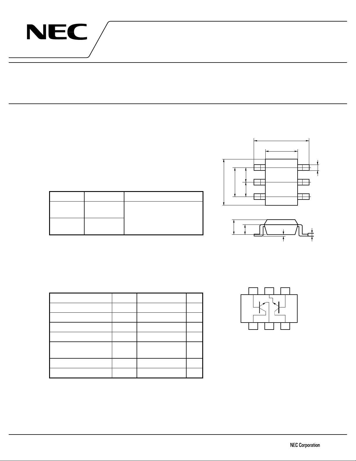
•6-pin thin-type small mini mold package adopted
•Built-in 2 transistors (2 u 2SC5184)
ORDERING INFORMATION
Part Number Quantity Packing Style
P
PA828TF Loose products
(50 pcs)
P
PA828TF-T1 Taping products
(3 kpcs/reel)
Remark
If you require an evaluation sample, please contact
an NEC Sales Representative (Unit sample quantity
is 50 pcs).
Embossed tape 8 mm wide.
Pin 6 (Q1 Base), Pin 5 (Q2
Emitter), Pin 4 (Q2 Base) face to
perforation side of the tape.
ABSOLUTE MAXIMUM RATINGS (TA = 25
PACKAGE DRAWINGS (Unit: mm)
2.10±0.1
1.25±0.1
+0.1
–0.05
0.22
0.13±0.05
1.30
2.00±0.2
0.60±0.1
0.65
0.65
0.45
R86
321
456
0 to 0.1
PIN CONFIGURATION (Top View)
C)
qqqq
B1
E2 B2
Parameter Symbol Rating Unit
Collector to Base Voltage V
Collector to Emitter Voltage V
Emitter to Base Voltage V
Collector Current I
Total Power Dissipation P
Junction Temperature T
Storage Temperature T
Caution is required concerning excess input, such as from static electricity, due to the high-precision
fabrication processes used for this device.
Document No. P12693EJ1V0DS00 (1st edition)
Date Published July 1997 N
Printed in Japan
CBO
CEO
EBO
C
T
90 in 1 element
180 in 2 elements
j
stg
The information in this document is subject to change without notice.
5V
3V
2V
30 mA
mW
150 °C
ð
65 to +150 °C
PIN CONNECTIONS
1. Collector(Q1)
2. Emitter(Q1)
3. Collector (Q2)
654
Q1 Q2
321
C1 E1 C2
4. Base (Q2)
5. Emitter(Q2)
6. Base (Q1)
1997©

PPPP
PA828TF
ELECTRICAL CHARACTERISTICS (T
A = 25°C)
Parameter Symbol Condition MIN. TYP. MAX. Unit
Collector Cutoff Current I
Emitter Cutoff Current I
DC Current Gain h
Gain Bandwidth Product (1) f
Gain Bandwidth Product (2) f
Feedback Capacitance C
Insertion Power Gain (1) |S
Insertion Power Gain (2) |S
CBO
EBO
21e
21e
VCB = 5 V, IE = 0 0.1
VEB = 1 V, IC = 0 0.1
VCE = 2 V, IC = 20 mA
FE
T
VCE = 2 V, IC = 20 mA, f = 2 GHz 9 11 GHz
T
VCE = 1 V, IC = 10 mA, f = 2 GHz 7 9 GHz
VCB = 2 V, IE = 0, f = 1 MHz
re
2
|
VCE = 2 V, IC = 20 mA, f = 2 GHz 7 8.5 dB
2
|
VCE = 1 V, IC = 10 mA, f = 2 GHz 6 7.5 dB
Note 1
Note 2
70 140
0.4 0.8 pF
Noise Figure (1) NF VCE = 2 V, IC = 3 mA, f = 2 GHz 1.3 2 dB
Noise Figure (2) NF VCE = 1 V, IC = 3 mA, f = 2 GHz 1.3 2 dB
hFE Ratio h
Notes 1.
Pulse measurement P
Capacitance between collector and base measured with a capacitance meter (auto-balancing bridge
2.
FE1/hFE2
VCE = 2 V, IC = 20 mA
FE
1 = smaller hFE value among Q1 and Q2
h
FE
2 = larger hFE value among Q1 and Q2
h
W
d 350 Ps, Duty cycle d 2%
0.85
method). Emitter should be connected to the guard pin of capacitance meter.
A
P
A
P
hFE CLASSIFICATION
Rank KB
Marking R86
hFE value 70 to 140
2

PPPP
PA828TF
TYPICAL CHARACTERISTICS (T
A = 25
C)
qqqq
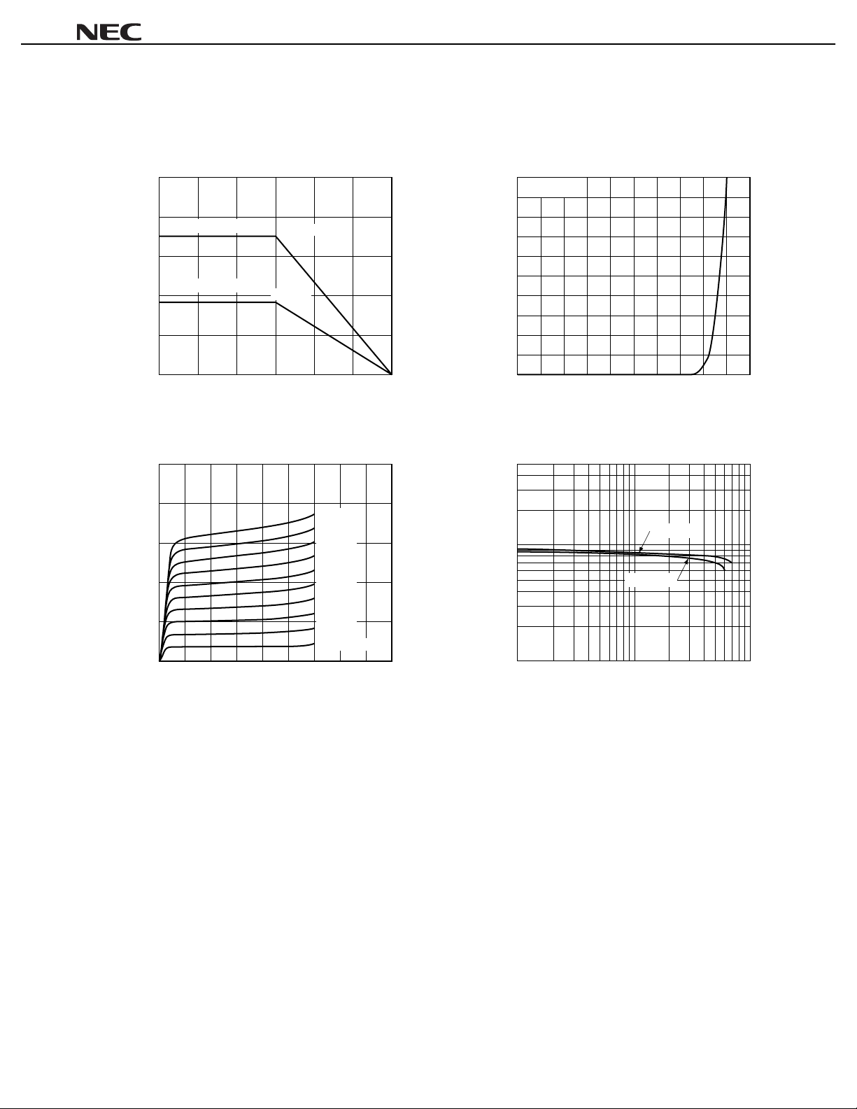
Total Power Dissipation vs. Ambient Temperature Collector Current vs. DC Base Voltage
50
VCE = 2 V
200
(mW)
T
100
Total Power Dissipation P
2 Elements in Total
Per Element
180 mW
90 mW
0 50 100 150
Ambient Temperature T
A
(˚C)
40
(mA)
C
30
20
10
Collector Current I
0 0.5 1.0
DC Base Voltage V
Collector Current vs. Collector to Emitter Voltage DC Current Gain vs. Collector Current
25
500
BE
(V)
20
(mA)
C
15
10
Collector Current I
5
0 1.0 2.0 3.0
Collector to Emitter Voltage V
µ
200 A
µ
180 A
µ
160 A
µ
140 A
µ
120 A
µ
100 A
µ
80 A
µ
60 A
40 A
µ
IB = 20 A
CE
µ
(V)
200
FE
VCE = 2 V
100
50
DC Current Gain h
VCE = 1 V
20
10
1 2 5 10 20 50 100
Collector Current I
C
(mA)
3

PPPP
PA828TF
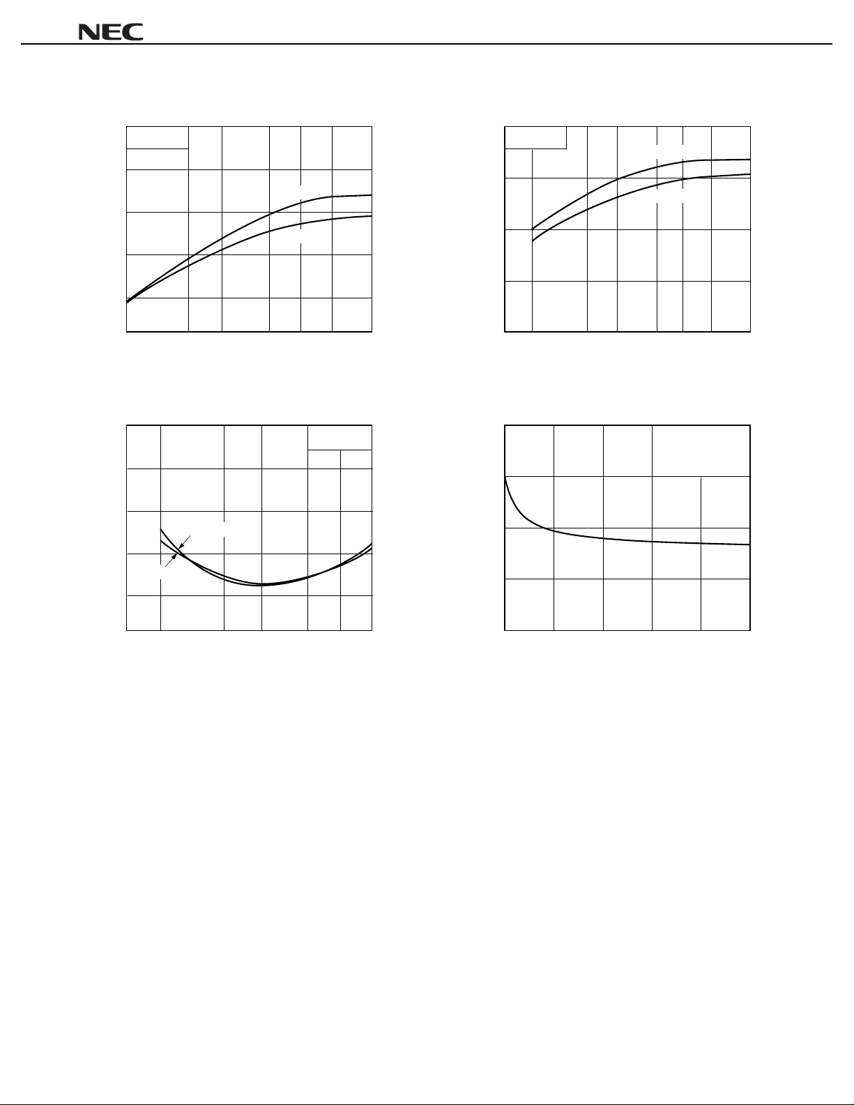
Gain Bandwidth Product vs. Collector Current Insertion Power Gain vs. Collector Current
15
f = 2 GHz
(GHz)
T
VCE = 2 V
10
VCE = 1 V
5
Gain Bandwidth Product f
123571020
Collector Current IC (mA)
Noise Figure vs. Collector Current Feedback Capacitance vs. Collector to Base Voltage
3
f = 2 GHz
2
VCE = 2 V
10
f = 2 GHz
(dB)
2
|
21e
5
Insertion Power Gain |S
0
123571020
Collector Current IC (mA)
0.8
(pF)
re
0.6
0.4
VCE = 2 V
V
CE
= 1 V
f = 1 MHz
Noise Figure NF (dB)
VCE = 1 V
1
1235710
Collector Current I
C
(mA)
0.2
Feedback Capacitance C
0 2.0 4.0 6.0 8.0 10.0
Collector to Base Voltage V
CB
(V)
4

S PARAMETER Q1
VCE = 2 V, IC = 1 mA, Z0 = 50
PPPP
PA828TF
:
FREQUENCY S
GHz MAG. ANG. MAG. ANG. MAG. ANG. MAG. ANG.
.10 .98
.20 .96
.30 .95
.40 .92
.50 .90
.60 .87
.70 .83
.80 .80
.90 .76
1.00 .72
1.10 .68
1.20 .64
1.30 .60
1.40 .56
1.50 .53
1.60 .50
1.70 .47
1.80 .45
1.90 .44
2.00 .43
2.10 .42
2.20 .41
2.30 .42 173.21 1.66 56.62 .20 20.78 .48
2.40 .42 165.82 1.61 53.39 .20 20.36 .47
2.50 .43 158.63 1.57 50.02 .20 20.11 .46
2.60 .44 152.11 1.52 47.07 .20 20.00 .45
2.70 .45 146.49 1.47 43.96 .20 19.86 .43
2.80 .46 140.70 1.43 41.06 .20 20.11 .43
2.90 .47 135.62 1.39 38.16 .20 20.18 .42
3.00 .48 131.49 1.35 35.61 .20 20.44 .41
11
6.87 2.42 171.77 .02 84.43 .99
ð
13.71 2.40 164.17 .04 79.61 .99
ð
20.79 2.42 157.17 .07 74.54 .97
ð
27.69 2.39 150.27 .09 69.50 .95
ð
34.82 2.39 143.98 .10 65.17 .92
ð
42.10 2.36 138.23 .12 60.29 .90
ð
49.35 2.34 132.19 .14 56.25 .87
ð
56.87 2.32 126.78 .15 52.12 .84
ð
64.78 2.32 120.75 .16 48.48 .81
ð
72.15 2.26 115.35 .17 45.16 .77
ð
80.50 2.25 110.20 .18 41.64 .75
ð
88.71 2.22 104.80 .18 38.79 .72
ð
97.33 2.16 99.84 .19 35.82 .69
ð
106.17 2.13 94.75 .19 33.51 .66
ð
115.63 2.10 89.64 .20 31.12 .63
ð
124.41 2.04 84.89 .20 29.04 .61
ð
133.52 1.99 80.39 .20 27.37 .59
ð
142.93 1.93 75.97 .20 25.64 .57
ð
152.17 1.87 71.81 .20 24.28 .55
ð
161.16 1.81 68.21 .20 23.31 .53
ð
170.55 1.77 63.89 .20 22.18 .51
ð
179.15 1.72 60.35 .20 21.50 .50
ð
21
S
12
S
22
S
4.42
ð
8.84
ð
12.97
ð
17.23
ð
21.05
ð
25.13
ð
28.47
ð
32.22
ð
34.98
ð
38.02
ð
40.84
ð
43.16
ð
45.68
ð
47.79
ð
49.93
ð
51.89
ð
53.75
ð
55.61
ð
57.34
ð
59.13
ð
60.65
ð
62.47
ð
64.18
ð
66.09
ð
67.98
ð
69.96
ð
72.10
ð
74.42
ð
76.70
ð
79.07
ð
5

S PARAMETER Q1
VCE = 2 V, IC = 3 mA, Z0 = 50
PPPP
PA828TF
:
FREQUENCY S
GHz MAG. ANG. MAG. ANG. MAG. ANG. MAG. ANG.
.10 .92
.20 .88
.30 .83
.40 .78
.50 .71
.60 .65
.70 .58
.80 .51
.90 .45
1.00 .40
1.10 .36
1.20 .32
1.30 .30
1.40 .27
1.50 .26
1.60 .25
1.70 .25
1.80 .26 174.75 2.95 67.58 .17 42.46 .35
1.90 .26 166.25 2.82 64.50 .17 41.71 .34
2.00 .27 158.59 2.69 61.59 .18 41.41 .32
2.10 .28 151.33 2.58 58.69 .19 40.78 .31
2.20 .29 145.02 2.47 56.03 .19 40.10 .30
2.30 .31 139.72 2.36 53.27 .20 39.55 .29
2.40 .32 134.63 2.28 50.82 .20 39.01 .28
2.50 .34 130.11 2.20 48.23 .21 38.47 .27
2.60 .35 126.08 2.12 45.78 .21 37.90 .26
2.70 .37 122.46 2.04 43.24 .22 37.28 .25
2.80 .38 119.06 1.97 41.09 .22 36.67 .24
2.90 .40 115.90 1.91 38.67 .23 35.90 .23
3.00 .41 113.18 1.85 36.49 .23 35.19 .22
11
10.76 6.79 166.90 .02 81.64 .97
ð
21.14 6.51 156.23 .04 74.96 .94
ð
31.82 6.40 146.87 .06 68.78 .88
ð
42.04 6.16 138.45 .07 63.27 .82
ð
52.43 5.95 130.70 .09 59.72 .76
ð
62.50 5.66 123.90 .10 55.61 .70
ð
72.69 5.43 116.65 .10 53.36 .65
ð
82.82 5.17 110.41 .11 51.17 .61
ð
92.60 4.88 104.31 .12 49.32 .57
ð
102.47 4.60 98.90 .12 48.24 .53
ð
112.48 4.34 94.04 .13 47.06 .50
ð
122.73 4.09 89.32 .14 46.16 .47
ð
133.29 3.85 85.28 .14 45.46 .45
ð
144.06 3.64 81.23 .15 44.88 .43
ð
155.19 3.45 77.48 .15 44.14 .41
ð
165.56 3.26 74.10 .16 43.48 .39
ð
175.58 3.10 70.82 .16 42.97 .37
ð
21
S
12
S
22
S
8.65
ð
16.65
ð
23.55
ð
29.88
ð
34.56
ð
39.19
ð
42.35
ð
45.67
ð
48.15
ð
50.32
ð
52.49
ð
54.24
ð
56.10
ð
57.94
ð
59.86
ð
61.58
ð
63.35
ð
65.35
ð
67.39
ð
69.29
ð
71.31
ð
73.78
ð
76.10
ð
78.86
ð
81.85
ð
84.98
ð
88.17
ð
91.66
ð
95.45
ð
99.22
ð
6
 Loading...