

Motorola SN54LS42J, SN74LS42D, SN74LS42N Datasheet
5-53
FAST AND LS TTL DATA
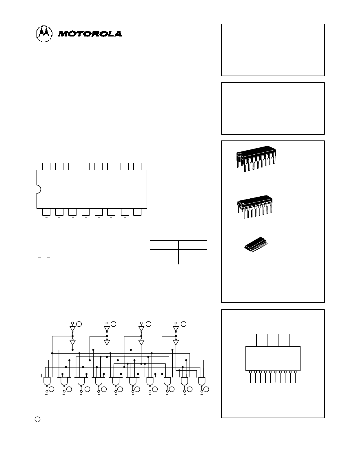
ONE-OF-TEN DECODER
The LSTTL/MSI SN54/74LS42 is a Multipurpose Decoder designed to accept four BCD inputs and provide ten mutually exclusive outputs. The LS42
is fabricated with the Schottky barrier diode process for high speed and is
completely compatible with all Motorola TTL families.
• Multifunction Capability
• Mutually Exclusive Outputs
• Demultiplexing Capability
• Input Clamp Diodes Limit High Speed Termination Effects
14 13 12 11 10 9
1 2 3 4 5 6
V
CC
7
16 15
8
A0A1A2A39
8 7
0 1 2 3 4 5 6 GND
NOTE:
The Flatpak version has the
same pinouts (Connection
Diagram) as the Dual In-Line
Package.
CONNECTION DIAGRAM DIP (TOP VIEW)
PIN NAMES LOADING (Note a)
HIGH
LOW
A0 – A
3
0
to 9
Address Inputs
Outputs, Active LOW (Note b)
0.5 U.L.
10 U.L.
0.25 U.L.
5(2.5) U.L.
NOTES:
a) 1 TTL Unit Load (U.L.) = 40 µA HIGH/1.6 mA LOW.
b) The Output LOW drive factor is 2.5 U.L. for Military (54) and 5 U.L. for Commercial (74)
Temperature Ranges.
3
LOGIC DIAGRAM
14
4 5 10 11
121315
1 2
6 7 9
1 2 3 4 5 60
A
0
A
1
A
2
A
3
987
VCC = PIN 16
GND = PIN 8
= PIN NUMBERS
SN54/74LS42
ONE-OF-TEN DECODER
LOW POWER SCHOTTKY
J SUFFIX
CERAMIC
CASE 620-09
N SUFFIX
PLASTIC
CASE 648-08
16
1
16
1
ORDERING INFORMATION
SN54LSXXJ Ceramic
SN74LSXXN Plastic
SN74LSXXD SOIC
16
1
D SUFFIX
SOIC
CASE 751B-03
LOGIC SYMBOL
VCC = PIN 16
GND = PIN 8
15 14 13 12
0 1 2 3 4 5 6 7 8 9
1 2 3 4 5 6 7 9 10 11
A0A1A2A
3
5-54
FAST AND LS TTL DATA
SN54/74LS42
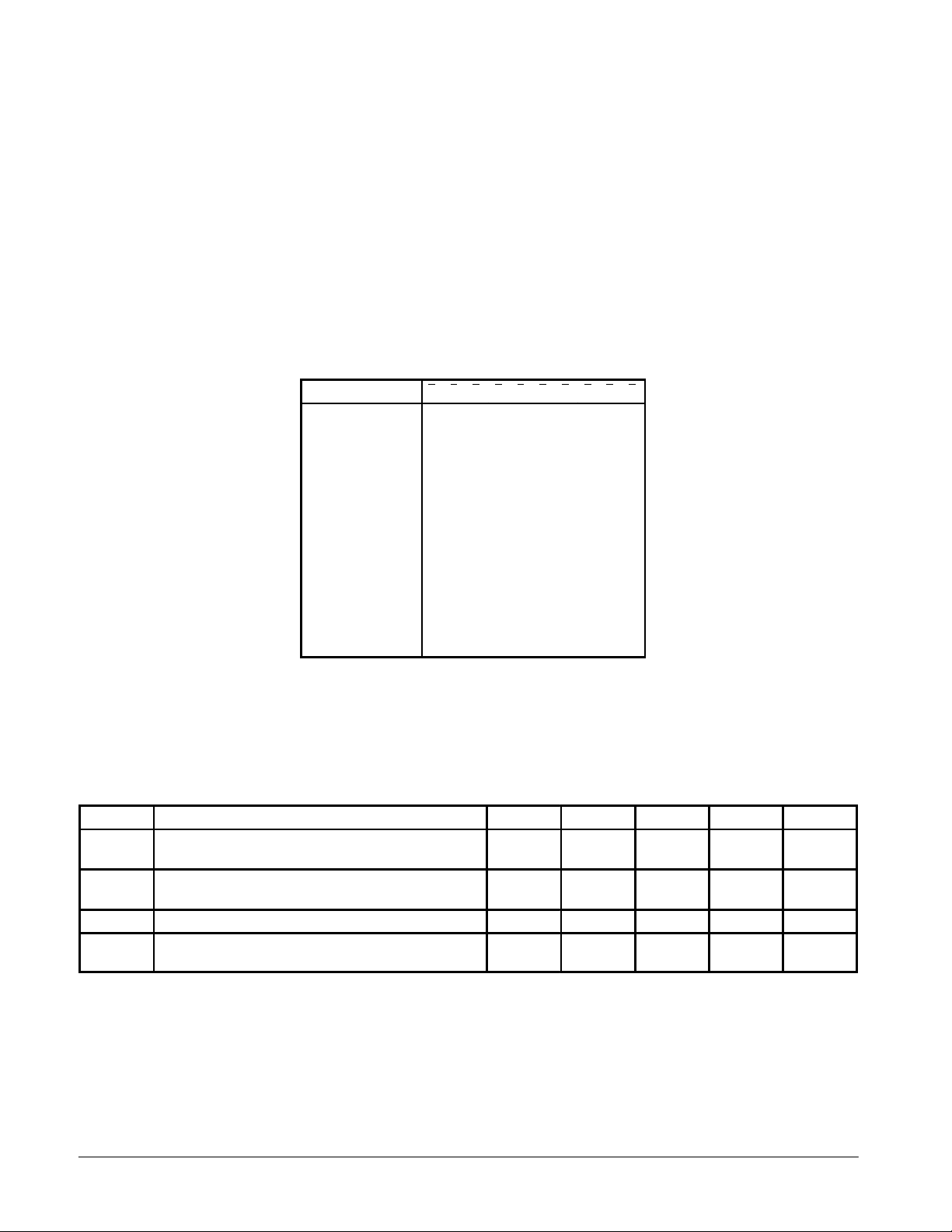
FUNCTIONAL DESCRIPTION
The LS42 decoder accepts four active HIGH BCD inputs
and provides ten mutually exclusive active LOW outputs, as
shown by logic symbol or diagram. The active LOW outputs
facilitate addressing other MSI units with LOW input enables.
The logic design of the LS42 ensures that all outputs
are HIGH when binary codes greater than nine are applied
to the inputs.
The most significant input A3 produces a useful inhibit func-
tion when the LS42 is used as a one-of-eight decoder. The A
3
input can also be used as the Data input in an 8-output
demultiplexer application.
TRUTH TABLE
A0A1A2A30 1 2 3 4 5 6 7 8 9
L
H
L
H
L
H
L
H
L
H
L
H
L
H
L
H
L
L
H
H
L
L
H
H
L
L
H
H
L
L
H
H
L
L
L
L
H
H
H
H
L
L
L
L
H
H
H
H
L
L
L
L
L
L
L
L
H
H
H
H
H
H
H
H
L
H
H
H
H
H
H
H
H
H
H
H
H
H
H
H
H
L
H
H
H
H
H
H
H
H
H
H
H
H
H
H
H
H
L
H
H
H
H
H
H
H
H
H
H
H
H
H
H
H
H
L
H
H
H
H
H
H
H
H
H
H
H
H
H
H
H
H
L
H
H
H
H
H
H
H
H
H
H
H
H
H
H
H
H
L
H
H
H
H
H
H
H
H
H
H
H
H
H
H
H
H
L
H
H
H
H
H
H
H
H
H
H
H
H
H
H
H
H
L
H
H
H
H
H
H
H
H
H
H
H
H
H
H
H
H
L
H
H
H
H
H
H
H
H
H
H
H
H
H
H
H
H
L
H
H
H
H
H
H
H = HIGH Voltage Level
L = LOW Voltage Level
GUARANTEED OPERATING RANGES
Symbol Parameter Min Typ Max Unit
V
CC
Supply Voltage 54
74
4.5
4.75
5.0
5.0
5.5
5.25
V
T
A
Operating Ambient Temperature Range 54
74
–55
0
25
25
125
70
°C
I
OH
Output Current — High 54, 74 –0.4 mA
I
OL
Output Current — Low 54
74
4.0
8.0
mA
 Loading...