

Motorola MC100LVEL16, MC100LVEL16D, MC100LVEL16DR2 Datasheet
MOTOROLA
SEMICONDUCTOR TECHNICAL DATA
Differential Receiver
The MC100L VEL16 is a differential receiver. The device is functionally
equivalent to the EL16 device, operating from a low voltage supply. The
LVEL16 exhibits a wider CMR range than its EL16 counterpart. With
output transition times and propagation delays comparable to the EL16
the L VEL16 is ideally suited for interfacing with high frequency sources at
3.3V supplies.
The L VEL16 provides a VBB output for either single-ended use or as a
DC bias for AC coupling to the device. The VBB pin should be used only
as a bias for the LVEL16 as its current sink/source capability is limited.
Whenever used, the VBB pin should be bypassed to ground via a 0.01µf
capacitor.
Under open input conditions, the Q input will be pulled down to Vee and
the Q
input will be biased to VCC/2. This condition will force the Q output
low.
MC100LVEL16
8
1
• 300ps Propagation Delay
• High Bandwidth Output Transitions
• 75kΩ Internal Input Pulldown Resistors
• >2000V ESD Protection
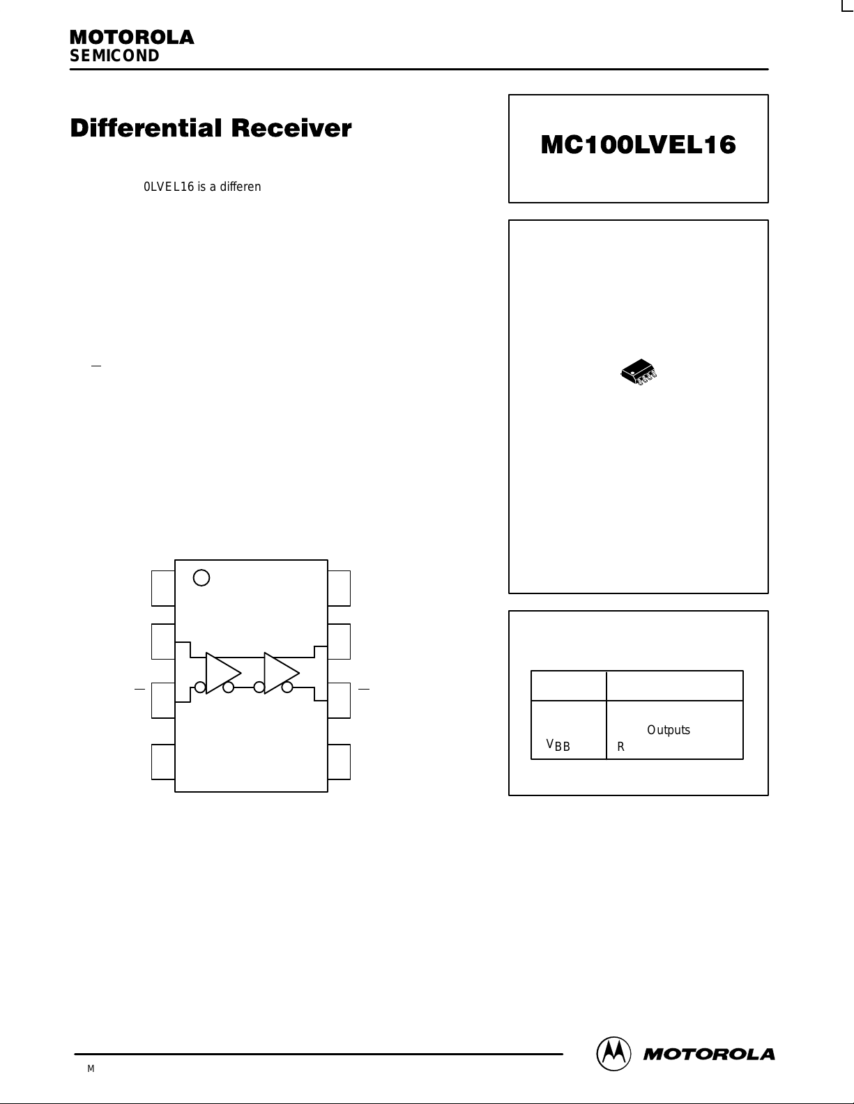
LOGIC DIAGRAM AND PINOUT ASSIGNMENT
1
NC
2
D
3
D
V
45
BB
V
8
CC
7
Q
6
Q
V
EE
D SUFFIX
PLASTIC SOIC PACKAGE
CASE 751-05
PIN DESCRIPTION
PIN FUNCTION
D Data Inputs
Q Data Outputs
V
BB Ref. Voltage Output
5/96
Motorola, Inc. 1996
4–1
REV 0

MC100LVEL16
DC CHARACTERISTICS (VEE = VEE(min) to VEE(max); VCC = GND)
–40°C 0°C 25°C 85°C
Symbol Characteristic Min Typ Max Min Typ Max Min Typ Max Min Typ Max Unit
I
EE
V
BB
V
EE
I
IH
I
IL
AC CHARACTERISTICS (VEE = VEE(min) to VEE(max); VCC = GND)
Symbol Characteristic Min Typ Max Min Typ Max Min Typ Max Min Typ Max Unit
t
PLH
t
PHL
t
SKEW
V
PP
V
CMR
t
r
t
f
1. Duty cycle skew is the difference between a TPLH and TPHL propagation delay through a device.
2. Minimum input swing for which AC parameters guaranteed. The device has a DC gain of ≈40.
3. The CMR range is referenced to the most positive side of the differential input signal. Normal operation is obtained if the HIGH level falls within
the specified range and the peak-to-peak voltage lies between VPPmin and 1V. The lower end of the CMR range varies 1:1 with VEE. The
numbers in the spec table assume a nominal VEE = –3.3V . Note for PECL operation, the V
Power Supply Current 17 23 17 23 17 23 18 24 mA
Output Reference Voltage –1.38 –1.26 –1.38 –1.26 –1.38 –1.26 –1.38 –1.26 V
Power Supply Voltage –3.0 –3.3 –3.8 –3.0 –3.3 –3.8 –3.0 –3.3 –3.8 –3.0 –3.3 –3.8 V
Input HIGH Current 150 150 150 150 µA
Input LOW Current DD0.5
Propagation Delay
to Output (Diff)
(SE)
Duty Cycle Skew1 (Diff) 5 30 5 20 5 20 5 20 ps
Minimum Input Swing
Common Mode Range
VPP < 500mV
VPP ≥ 500mV
Output Rise/Fall Times Q
(20% – 80%)
–600
–40°C 0°C 25°C 85°C
150
275
275
400
450
–0.4
–0.4
100
2
150 150 150 150 mV
3
–2.0
–1.8
120 220 320 120 220 320 120 220 320 120 220 320 ps
0.5
–600
215
165
–2.1
–1.9
290
290
365
415
–0.4
–0.4
0.5
–600
225
175
–2.1
–1.9
0.5
–600
300
375
425
–0.4
–0.4
240
190
–2.1
–1.9
300
(min) will be fixed at 3.3V – |V
CMR
315
315
390
440
–0.4
–0.4
CMR
µA
ps
V
(min)|.
MOTOROLA ECLinPS and ECLinPS Lite
4–2
DL140 — Rev 3
 Loading...