


LAC-5800
MODELS : LAC5800(R)/LAC5810/LAC-UA580R
CAUTION
BEFORE SERVICING THE UNIT, READ THE “SAFETY PRECAUTIONS”
IN THIS MANUAL
.
MODELS : LAC5800(R)/LAC5810/LAC-UA580R
SERVICE MANUAL
P/NO : AFN36957742
Website http://biz.lgservice.com
Internal Use Only
CAR CD/MP3/WMA
RECEIVER
SERVICE MANUAL
FEBRUARY, 2008

1-1
CONTENTS
SECTION 1 SUMMARY
SERVICING PRECAUTIONS .........................................................................................................................1-2
ESD PRECAUTIONS ......................................................................................................................................1-3
SPECIFICATIONS ...........................................................................................................................................1-4
FIRMWARE UPGRADE METHOD.................................................................................................................1-5
HOW TO CONNECT AUDIO SET TO POWER SUPPLY............................................................................1-7
SECTION 2 ELECTRICAL
ELECTRICAL TROUBLESHOOTING GUIDE & WAVEFORMS.................................................................2-1
1. MAIN, FRONT & TUNER PART................................................................................................................2-1
2. CDP PART.................................................................................................................................................2-4
3. USB PART.................................................................................................................................................2-7
• CIRCUIT VOLTAGE CHART......................................................................................................................2-9
• WAVEFORMS ...........................................................................................................................................2-10
INTERNAL BLOCK DIAGRAM OF ICs ......................................................................................................2-12
1. IC301 (HA13173AH) ...............................................................................................................................2-12
2. IC402 (µPD78F1165) ..............................................................................................................................2-14
3. IC503 (LC786923W) ...............................................................................................................................2-17
4. IC504 (AM5810) ......................................................................................................................................2-22
5. IC601 (BD3805F) ....................................................................................................................................2-24
6. IC801 (TB2926HQ) .................................................................................................................................2-25
7. IC901 (PT6524).......................................................................................................................................2-26
BLOCK DIAGRAM ........................................................................................................................................2-29
CIRCUIT DIAGRAMS....................................................................................................................................2-31
1. MAIN CIRCUIT DIAGRAM ......................................................................................................................2-31
2. FRONT CIRCUIT DIAGRAM...................................................................................................................2-33
3. CDP-1 CIRCUIT DIAGRAM ....................................................................................................................2-35
4. CDP-2 CIRCUIT DIAGRAM ....................................................................................................................2-37
5. AUX CIRCUIT DIAGRAM........................................................................................................................2-39
PRINTED CIRCUIT BOARD DIAGRAMS...................................................................................................2-41
1. MAIN P.C.BOARD(TOP VIEW) ...............................................................................................................2-41
2. MAIN P.C.BOARD(BOTTOM VIEW) .......................................................................................................2-43
3. FRONT P.C.BOARD................................................................................................................................2-45
4. CDP P.C.BOARD.....................................................................................................................................2-47
5. AUX P.C. BOARD....................................................................................................................................2-49
SECTION 3 EXPLODED VIEWS
1. CABINET AND MAIN FRAME SECTION..................................................................................................3-1
2. MECHANISM(PICK-UP) SECTION ..........................................................................................................3-3
SECTION 4 REPLACEMENT PARTS LIST.................................................4-1
Copyright © 2008 LG Electronics. Inc. All right reserved.
Only for training and service purposes
LGE Internal Use Only

1-2
1. Always disconnect the power source before:
1) Removing or reinstalling any component, circuit board, module or any other instrument assembly.
2) Disconnecting or reconnecting any instrument electrical plug or other electrical connection.
3) Connecting a test substitute in parallel with an electrolytic capacitor in the instrument.
CAUTION: A wrong part substitution or incorrect polarity installation of electrolytic capacitors may result in an
explosion hazard.
2. Do not defeat any plug/socket B+ voltage interlocks with which instruments covered by this service
manual might be equipped.
3. Do not apply power to this instrument and or any of its electrical assemblies unless all solid-state
device heat sinks are correctly installed.
4. Always connect a test instrument’s ground lead to the instrument chassis ground before connecting
the test instrument positive lead. Always remove the test instrument ground lead last.
1) The service precautions are indicated or printed on the cabinet, chassis or components. When servicing,
follow the printed or indicated service precautions and service materials.
2) The Components used in the unit have a specified conflammability and dielectric strength. When replacing
any components, use components which have the same ratings. Components marked in the circuit diagram
are important for safety or for the characteristics of the unit. Always replace with the exact components.
3) An insulation tube or tape is sometimes used and some components are raised above the printed writing
board for safety. The internal wiring is sometimes clamped to prevent contact with heating components.
Install them as they were.
4) After servicing always check that the removed screws, components and wiring have been installed correctly
and that the portion around the service part has not been damaged. Further check the insulation between
the blades of attachment plug and accessible conductive parts.
SECTION 1 SUMMARY
SERVICING PRECAUTIONS
Copyright © 2008 LG Electronics. Inc. All right reserved.
Only for training and service purposes
LGE Internal Use Only
1-3
ESD PRECAUTIONS
Electrostatically Sensitive Devices (ESD)
Some semiconductor (solid state) devices can be damaged easily by static electricity. Such components
commonly are called electrostatically sensitive devices (ESD). Examples of typical ESD devices are inte-
grated circuits and some field-effect transistors and semiconductor chip components. The following tech-
niques should be used to help reduce the incidence of component damage caused by static electricity.
1. Immediately before handling any semiconductor component or semiconductor-equipped assembly,
drain off any electrostatic charge on your body by touching a know earth ground. Alternatively, obtain
and wear a commercially available discharging wrist strap device, which should be removed for poten-
tial shock reasons prior to applying power to the unit under test.
2. After removing an electrical assembly equipped with ESD devices, place the assembly on a conductive
surface such as aluminum foil, to prevent electrostatic charge buildup or exposure of the assembly.
3. Use only a grounded-tip soldering iron to solder or unsolder ESD devices.
4. Use only an anti-static solder removal device. Some solder removal devices not classified as "anti-stat-
ic" can generate electrical charges sufficient to damage ESD devices.
5. Do not use freon-propelled chemicals These can generate electrical charges sufficient to damage ESD
devices.
6. Do not remove a replacement ESD device from its protective package until immediately before you are
ready to install it. (Most replacement ESD devices are packaged with leads electrically shorted together
by conductive foam, aluminum foil or comparable conductive materials).
7. Immediately before removing the protective material from the leads of a replacement ESD device, touch
the protective material to the chassis or circuit assembly into which the device will by installed.
CAUTION : BE SURE NO POWER IS APPLIED TO THE CHASSIS OR CIRCUIT, AND OBSERVE
ALL OTHER SAFETY PRECAUTIONS.
8. Minimize bodily motions when handing unpackaged replacement ESD devices. (Otherwise harmless
motion such as the brushing together of your clothes fabric or the lifting of your foot from a carpeted
floor can generate static electricity sufficient to damage an ESD device).
CAUTION. GRAPHIC SYMBOLS
THE LIGHTNING FLASH WITH ARROWHEAD SYMBOL. WITHIN AN EQUILATERAL
TRIANGLE, IS INTENDED TO ALERT THE SERVICE PERSONNEL TO THE PRESENCE
OF UNINSULATED "DANGEROUS VOLTAGE" THAT MAY BE OF SUFFICIENT MAGNI-
TUDE TO CONSTITUTE A RISK OF ELECTRIC SHOCK.
THE EXCLAMATION POINT WITHIN AN EQUILATERAL TRIANGLE IS INTENED TO
ALERT THE SERVICE PERSONNEL TO THE PRESENCE OF IMPORTANT SAFETY
INFORMATION IN SERVICE LITERATURE.
Copyright © 2008 LG Electronics. Inc. All right reserved.
Only for training and service purposes
LGE Internal Use Only

1-4
SPECIFICATIONS
• GENERAL
Output Power 50W x 4CH (Max.)
Power Source DC 12V
Speaker impedance 4Ω
Ground System Negative
Dimensions (WxHxD) 180 x 50 x 176 mm (Without Control Panel)
Net Weight 1.3 kg
• CD SECTION
Frequency Response 20 Hz-20 kHz
S/N Ratio 80 dB
Distortion 0.12%
Channel Separation (1kHz) 55 dB
• RADIO SECTION
FM
Frequency Range 87.5-107.9, 87.5-108, 65-74 or 87.5-108 MHz
S/N Ratio 55 dB
Distortion 0.7%
Usable Sensitivity 12 dBµV
AM (MW)
Frequency Range 520-1720 or 522-1620 kHz
S/N Ratio 50 dB
Distortion 1.0%
Usable Sensitivity 28 dBµV
• AUX
Frequency Response 20 Hz-20 kHz
S/N Ratio 80 dB
Distortion 0.12 %
Channel Separation (1kHz) 45 dB
Max Input Level (1kHz) 1.2V (35KΩ)
Copyright © 2008 LG Electronics. Inc. All right reserved.
Only for training and service purposes
LGE Internal Use Only

1-5
[ MAIN/CD FIRMWARE UPGRADE ]
FIRMWARE UPGRADE METHOD
1. Confirmation of version information
• Change the Source of audio set to tuner.
(Default: tuner)
• Turn power off using power key.
• Press power key for 5 sec.
(After power on, continue pressing)
• After 5 sec, beep sound rings two times.
Then version information would show up at
display.
• In order to check version of MAIN/CD system,
Press band key.
• With beep Sound version of system for main,
CD is displayed in sequence.
2. Upgrade Program reading
• Insert update CD in ACC on state and then
[READING --> FILE CHK --> DOWNLORD?]
is displayed in order
3. Upgrade start
• In order to start upgrade, Press INT key long
(more then 2 sec) until “CHECK CD” Display
on the LCD.
4. Upgrade progress display
• Upgrade is in progress now.
[ Write --> I-VRF --> D-VRF ]
5. Upgrade Completion
• When Upgrade finished, the display shows up
“DOWNLOADED”. After a while, the audio set
is reset automatically.
•
Caution!
If power is off on the way of upgrading
firmware, the set can’t be recovered.
Therefore pay lots of attention for power not to
be off.
Copyright © 2008 LG Electronics. Inc. All right reserved.
Only for training and service purposes
LGE Internal Use Only
1-6
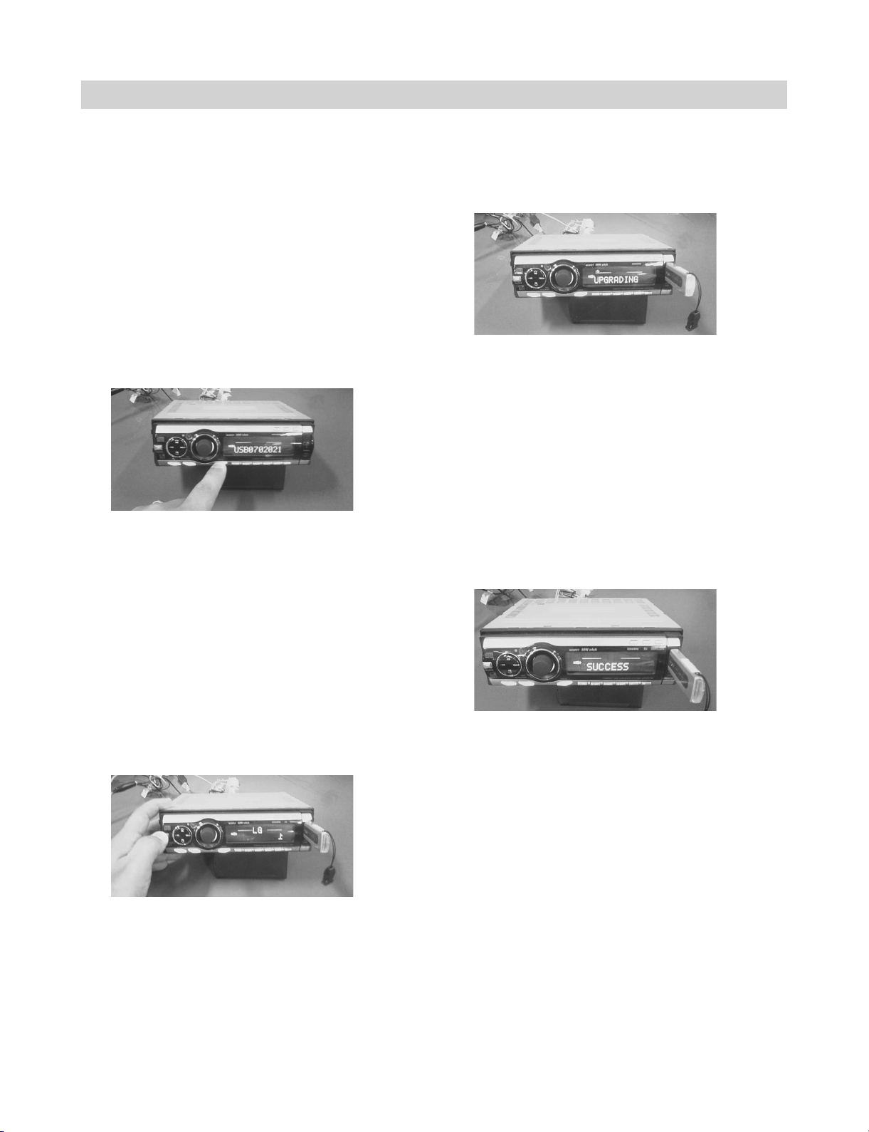
1. Confirmation of version information
• Change the source of audio set to tuner.
(default : tuner)
• Turn power off using power key.
• Press power key for 5 secs.
(After power is on, continue pressing)
• After 5 secs, beep sound rings two times.
Then the version information would show up
at display.
• In order to check version of USB system,
press band key. With beep sound, version of
systems for main, CD and USB is displayed in
sequence.
2. Upgrade Preparation
• At first check that audio set is in tuner mode.
With power key, turn it off. Make it sure to
insert USB device which has upgrade file.
3. Upgrade start
• Press SRC key for 5 secs. After power is on,
continue pressing. And then the audio set is
changed to USB upgrade mode.
4. Upgrade progress display
• Upgrade is in progress now.
It takes about 10 secs.
5. Upgrade completion
• Upgrade finished, the right display shows up.
After a while, the audio set is reset automati-
cally.
•
Caution!
If power is off on the way of upgrading
firmware, the set can’t be recovered.
Therefore pay lots of attention for power not to
be off.
[ USB FIRMWARE UPGRADE ]
Copyright © 2008 LG Electronics. Inc. All right reserved.
Only for training and service purposes
LGE Internal Use Only
1-7
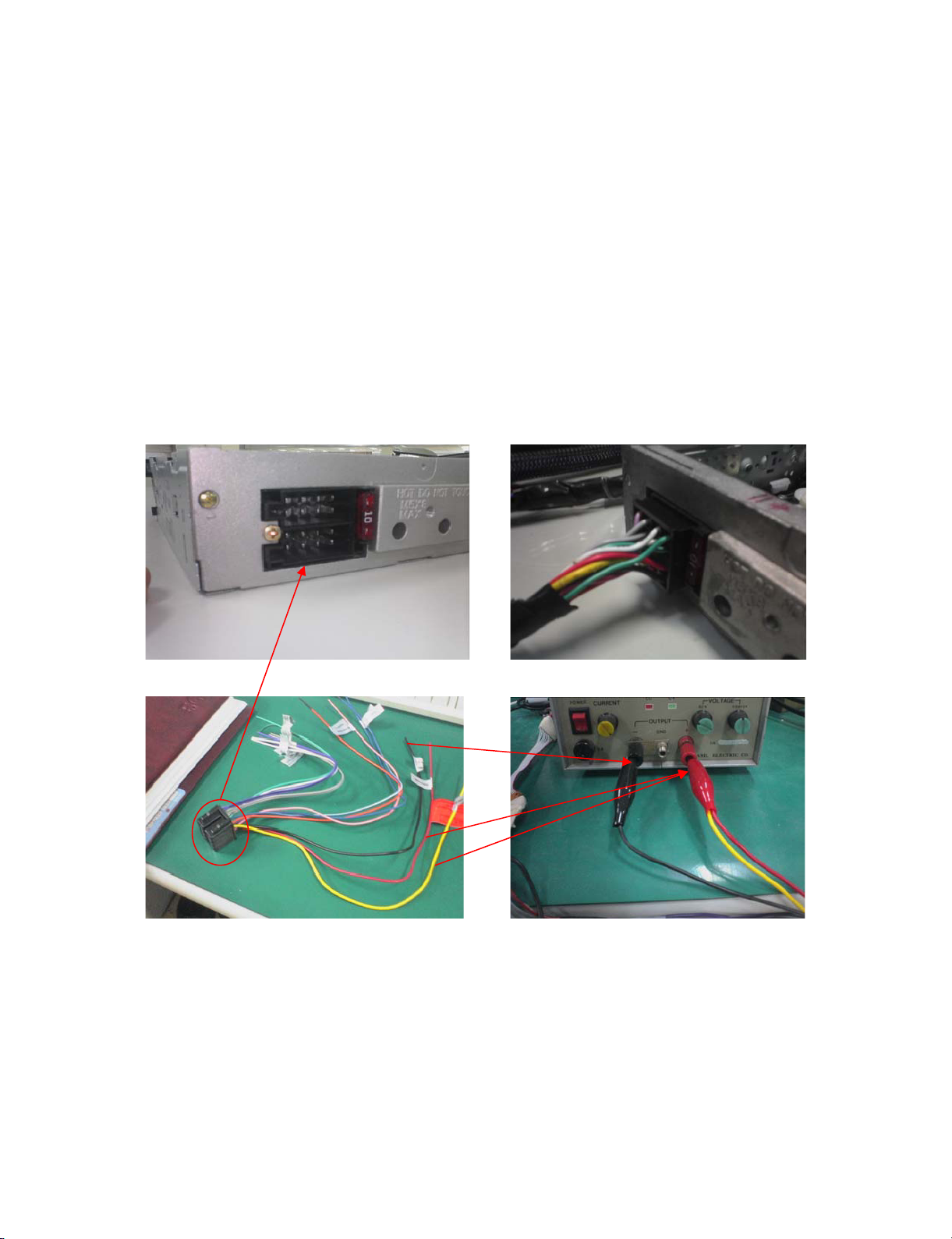
HOW TO CONNECT AUDIO SET TO POWER SUPPLY
• It is sufficient only to supply power for upgrade.
• Shown from the right figure, connect yellow line (Battery) and red line (Ignition) to plus and
minus terminal respectively.
• Jack is connected to the audio set via its shapes matched each other.
• We need power supply for operation of audio set (Voltage : 12~15V Current : Over 2A)
Before connection between set and power supply, adjust voltage level to 15V typically
(It is okay up to 12V.)
Power Supply has a variety of shapes and capacity of voltage and current.
At first check these things.
Copyright © 2008 LG Electronics. Inc. All right reserved.
Only for training and service purposes
LGE Internal Use Only
1-8
Copyright © 2008 LG Electronics. Inc. All right reserved.
Only for training and service purposes
LGE Internal Use Only

2-1
SECTION 2 ELECTRICAL
ELECTRICAL TROUBLESHOOTING GUIDE & WAVEFORMS
SYSTEM CONTROL
1. MAIN, FRONT & TUNER PART
No Symptom Check Point Location No.
1 No Power Checked the Fuse. CN302
Checked the Back up Vdd, Gnd. CN302(15,16)
Checked the Micom Back Up Vdd. IC301(14), D428,
IC402(30,47,50,99,100)
Checked the Micom Ground. IC402(20,51,97,98)
Checked the Reset. IC401, IC402(90)
Checked the X-tal. X401, X402
Checked the ACC In. Q301, Q302, IC402(40), CN302(14)
Checked the Detachable Switch. SW400, IC402(70)
Checked the Flipdown Switch. CN407(24), IC402(69)
Checked the Key Line. IC402(52,53)
2 Not available Remocon
Checked the Remocon Sens Vdd, Line.
CN404(5), IC402(81), RM901
3 Not available to Volume Control Checked the Encoder Volume. EV901, IC402(74,75)
4 Not available to Key Control Checked Tact Switch. SW901 ~ SW909, SW911 ~ SW919
Checked Key Line. IC402(52,53)
5 No sound Checked the E-VR Vdd. IC601(15)
Checked the E-VR Ground. IC601(1,22)
Checked the E-VR Control. IC601(20,21), IC402(3,4)
Checked the E-VR Signal In/Out. IC601(3,4,5,6,7,10,11)
IC601(12,13,14,15)
Checked the E-VR Mute Control IC601(19), IC402(14)
Checked the Power IC Vdd. IC801(6,20)
Checked the Power IC Ground. IC801(1,2,8,13,18,24)
Checked the Power IC Control. IC801(4,22), IC402(17,18)
Checked the Power IC Signal In/Out. IC801(11,12,14,15)
IC801(3,5,7,9,17,19,21,23)
6 No Line out signal Checked the E-VR Output. IC601(12,13,14,15)
Checked the Output. JK601
7 Not avaliable to Telephone Mute Checked the Telephone Mute Control. CN406(2)
Checked the Mute Control. IC402(38), Q312, Q313
8 Not avaliable to Checked the ANT Control. CN302(10), IC301(12,13), IC402(35)
ANT(Motor Type) Control
9 Not avaliable to Remote Checked the Remote Control. IC301(2), CN406(1), Q311
(Power AMP)
10 No output Beep sound. Checked the Beep Control. IC402(80), R801
Copyright © 2008 LG Electronics. Inc. All right reserved.
Only for training and service purposes
LGE Internal Use Only
DISPLAY & LIGHTING
TUNER FUNCTION
2-2
No Symptom Check Point Location No.
1 No Display or Some Checked the LCD DRV Vdd. Q307, D425, IC901(56,57,58)
Display is Broken Checked the LCD DRV Ground. IC901(59)
Checked the LCD DRV OSC. IC901(60)
Checked the LCD DRV Control. IC402(73,76,78,79)
IC901(61,62,63,64)
Checked the LCD DRV to IC901(1~55)
LCD Pattern.
2 No LCD Lighting or Checked the LCD Lighting VDD. IC301(4,9), Q303
Color is different Checked the LED. LD961, LD962
3 Not avaliable to Checked the LCD Lighting Control. Q305, ZD426, CN302(11)
LCD Lighting Control Checked the LED. LD901 ~ LD923, LD931 ~ LD953
4 Don't moved Level Bar Checked the Level Meter Control. IC402(56,57,58)
5 Not avaliable to Dimmer Control Chekced the Dimmer Control. IC402(49), CN302(11), ZD426, Q305
1 Not available to Tuner Checked the Tuner Vdd. TU201(6,17), Q309, Q310
Checked the Tuner Ground. TU201(3,7,12,16)
Checked the PLL data. TU201(9,14,15,19,20)
IC402(1,2,5,6,55)
Checked the RF signal in. TU201(1,2)
Checked the S-Meter Control TU201(5)
2Tuner no sound Checked the Tuner Signal Out. TU201(10,11,12), IC601(10,11)
Checked the AF mute. TU201(8), IC402(7)
3 Not available to RDS Checked the RDS data. TU201(19,20), IC402(5,6)
Copyright © 2008 LG Electronics. Inc. All right reserved.
Only for training and service purposes
LGE Internal Use Only
2-3
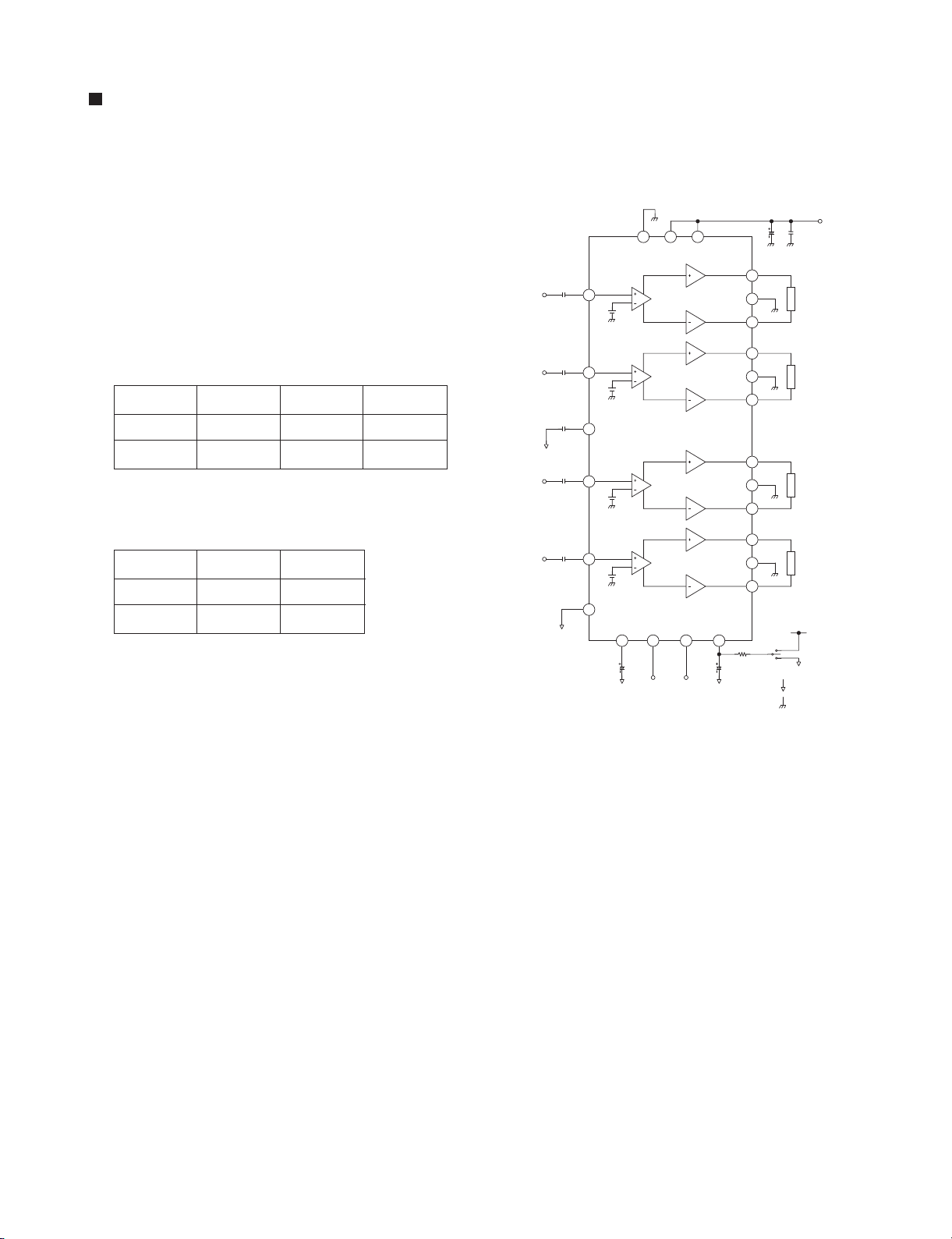
CAUTION - Tip for repair
Before exchange power amp IC(TB2926) for no audio problem, you have to check
below list.
1. Check VCC (pin 20,6) & GND
2. Check input pin 11,12,14,15
3. Check Standby, pin 4
: Follow the below list.
4. Check Mute function, pin 22
: Follow the below list.
5. Check Ripple pin 10.
: Normally it is high (about 10V)
6. Re-soldering all the pin of IC.
: Prevent crack of solder line.
* Keep changed IC, We request that you send it to HQ.
R
L
R
L
R
L
11
9
8
7
5
2
3
17
18
19
21
24
23
12
15
14
1 20 6
R
L
IN1
IN2
IN3
IN4
13
C
1
C
1
C
1
C
1
PRE-GND
10 25 22
OUT1
+
+
+
+
-
-
-
-
()
PW-GND1
OUT1 ( )
OUT2 ( )
PW-GND2
OUT2 ( )
OUT3 ( )
PW-GND3
OUT3 ( )
OUT4 ( )
PW-GND4
OUT4 ( )
TAB V
CC1
V
CC2
C
3
C
4
C
2
: PRE-GND
: PW-GND
STBYRIP
MUTE
C
5
16
C
6
4
OFF-SET
DET
MUTE
PLAY
5 V
R
1
AC-GND
Stand-by Power Sound Voltage
ON OFF OFF 0 to 1.5
OFF ON ON 3.5 to 6V
Mute Sound Voltage
ON OFF 0 to 1.5
OFF ON 3.5 to 6V
Picture 1) Power IC desc.
Copyright © 2008 LG Electronics. Inc. All right reserved.
Only for training and service purposes
LGE Internal Use Only
2-4
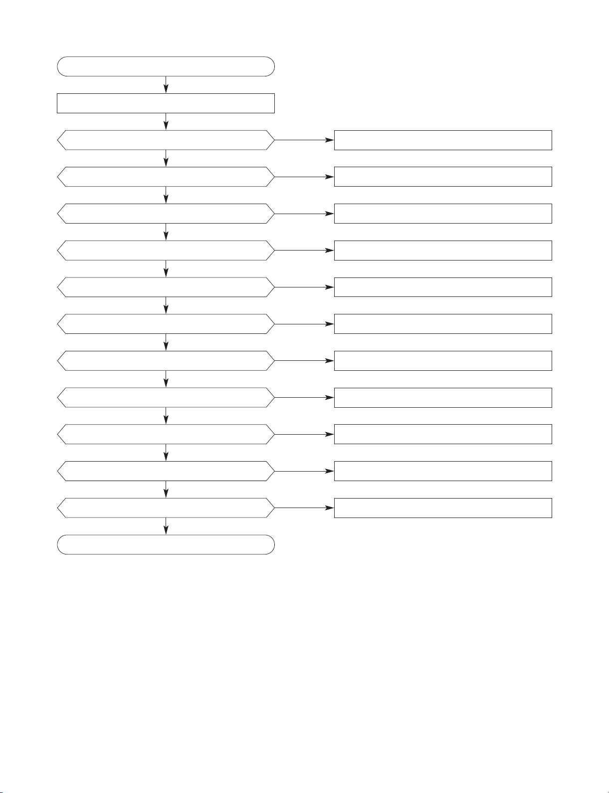
2. CDP PART
YES
YES
NO
CN520(6,29)
NO
IC503(28,42,60,72,81,123,143)
NO
IC504(7,8,20)
NO
IC504(88)
NO
NO
X501
Fig 1, 2
Fig 3, 4
Fig 1, 2
CN506(2)
NO
CN520(12,17)
NO
CN506(1)
No Loading?
YES
Checked the CD Vdd?
YES
Checked the CD DSP Ground?
YES
Checked the Motor DRV VDD?
YES
Checked the CD DSP Reset?
YES
Checked the CD DSP X-tal?
YES
Checked the Disc in load switch?
YES
Checked the Loading Motor Control?
YES
Checked the 12/8Cm sens switch?
OK
Something wrong With the CD Player?
Copyright © 2008 LG Electronics. Inc. All right reserved.
Only for training and service purposes
LGE Internal Use Only
2-5
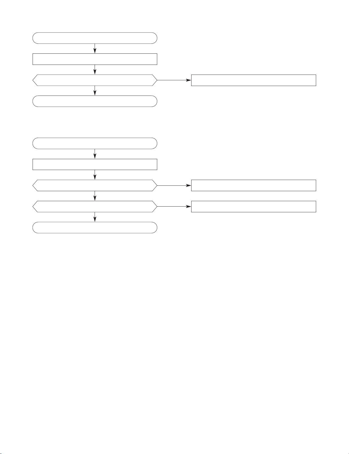
YES
YES
NO
CN506(8)
NO
IC504(21)
NO
CN520(12,17)
NO
IC503(84,85,86,87)
NO
NO
IC503(38), IC504(15,16)
Fig 5
Fig 5
Fig 10~ 11
Fig 3, 4
Fig 1, 2
Fig 12
Fig 9
IC503(17)
NO
CN520(25)
NO
NO
IC503(8)
Fig 7
IC503(41), IC504(11,12)
NO
Fig 8
IC503(40), IC504(13,14)
NO
Fig 6
IC503(39), IC504(17,18)
No Reading & "FILE CHECK" DISPLAY?
YES
Checked the Limit switch?
YES
Checked the Motor DRV mute control?
YES
Checked the Motor LODING Control?
YES
Checked the CD DSP Control?
YES
Checked the focus control?
YES
Checked the focus error level out.(FE Mon)?
YES
Checked the PLL locking.(FSEQ)?
YES
Checked the RF signal out check?
YES
Checked the spindle motor control?
YES
Checked the SLED control?
YES
Checked the tracking control?
OK
Something wrong With the CD Player?
Copyright © 2008 LG Electronics. Inc. All right reserved.
Only for training and service purposes
LGE Internal Use Only
2-6
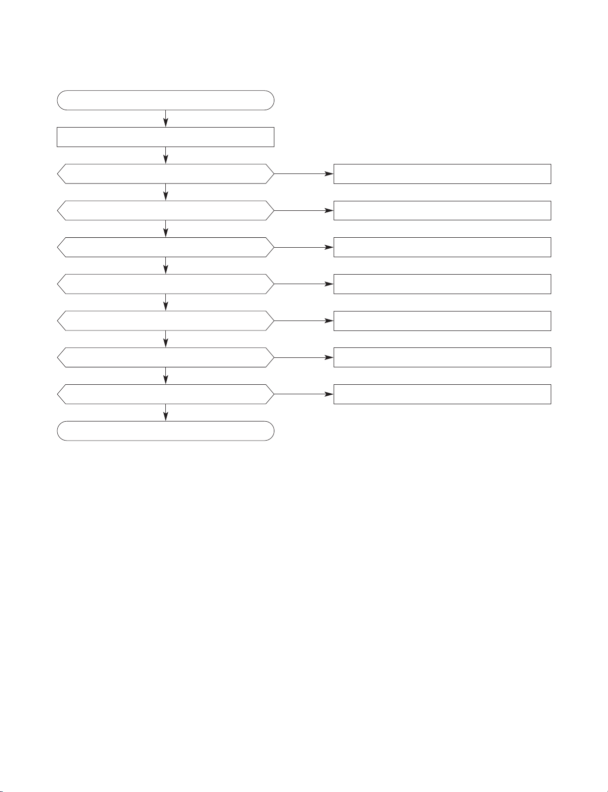
YES
YES
NO
IC503(140,141)
CD no sound?
YES
Checked the DSP signal out?
OK
Something wrong With the CD Player?
YES
YES
NO
CN403(1)[MAIN]
NO
CN520(12,17)
Fig 3,4
No ejected the CD?
YES
Checked the Eject key?
YES
Checked the Loading Motor Control?
OK
Something wrong With the CD Player?
Copyright © 2008 LG Electronics. Inc. All right reserved.
Only for training and service purposes
LGE Internal Use Only
2-7
3. USB PART
YES
YES
NO
IC711(8,18,39)
NO
IC711(5,19,40)
NO
PN703(5)
NO
X701
NO
NO
IC711(38,37)
Fig 13
PN703(4)
NO
IC711(9,10,11,14)
Only "NO USB" or "USB CHECK" Display?
YES
Checked the USB Vdd?
YES
Checked the USB interface IC Ground?
YES
Checked the USB interface IC reset?
YES
Checked the USB interface IC X-tal?
YES
Checked the D+/D Port?
YES
Checked the USB indication Port?
YES
Checked the USB interface IC control?
OK
Something wrong with the USB?
Copyright © 2008 LG Electronics. Inc. All right reserved.
Only for training and service purposes
LGE Internal Use Only
 Loading...