


GW520
Service Manual Model : GW520
Internal Use Only
Service Manual
GW520
Date: July, 2009 / Issue 1.1

- 3 -
Copyright © 2009 LG Electronics. Inc. All right reserved.
Only for training and service purposes
LGE Internal Use Only
Table Of Contents
1. INTRODUCTION ...............................................5
1.1 Purpose ......................................................................5
1.2 Regulatory Information .................................................5
1.3. ABBREVIATION ...........................................................7
2. PERFORMANCE ...............................................9
2.1 Supporting Standard ....................................................9
2.2 Main Parts : Solution ..................................................10
2.3 H/W features .............................................................10
2.4 HW Spec. ................................................................12
3. BB CIRCUIT TECHNICAL BRIEF ..................... 17
3.1 Functional Block Diagram ..........................................17
3.2 Baseband Processor Introduction ...............................18
3.3 Power management IC...............................................31
3.4. Power ON/OFF .........................................................39
3.5 SIM Interface .............................................................40
3.6 MICRO SD connector .................................................41
3.7 Memory ....................................................................42
3.8 LCD Display ..............................................................43
3.9 Keypad switching & scanning .....................................44
3.10 keypad back-light illumination ..................................45
3.11 LCD back-light illumination ......................................47
3.12 Battery voltage monitor ............................................48
3.13 Audio ......................................................................49
3.14 Bluetooth/FM (RBCA-B561A)....................................51
3.15 5PIN Interface connector ..........................................53
4. RF Circuit Technical Brief ............................54
4.1 General Description ...................................................54
4.2 GSM Part ..................................................................58
4.3 WCDMA Part .............................................................62
4.4 GSM Power Amplifi er Module .....................................65
4.5 WCDMA Band1/8 Power Amplifi er Module ..................66
4.6 WCDMA Band1/8 Low Noise Amplifi er ........................67
4.7 WCDMA Band1 Duplexer ...........................................68
4.8 WCDMA Band8 Duplexer ...........................................68
5. Trouble shooting .......................................... 69
5.1 Trouble shooting test setup ........................................69
5.2. Power on trouble ......................................................70
5.3 Charging Trouble .......................................................73
5.4 USB Trouble ..............................................................75
5.5 SIM Detect Trouble ....................................................78
5.6 Qwerty Key Sense Trouble ..........................................81
5.7 Slide Key sense Trouble .............................................83
5.8 Keypad backlight Trouble ...........................................84
5.9 Micro SD Trouble .......................................................86
5.10 Audio Trouble ..........................................................88
5.11 Microphone Trouble .................................................92
5.12 Camera Trouble .......................................................94
5.13 Main LCD Trouble ....................................................96
5.14 Bluetooth Trouble .....................................................98
5.15 RF Component ......................................................101
5.16 GSM PATH ............................................................103
5.17 Trouble Shooting of GSM Part .................................103
5.18 Trouble Shooting of WCDMA Part ............................112
6. Download & S/W upgrade ......................... 118
7. BLOCK DIAGRAM ........................................ 148
8. CIRCUIT DIAGRAM ...................................... 149
9. BGA Pin Map .............................................. 157
10. PCB LAYOUT .............................................161
11. RF Calibration .......................................... 167
11.1. Test Equipment Setup ...........................................167
11.2. Calibration Step ....................................................167
12. EXPLODED VIEW & REPLACEMENT
PART LIST ................................................ 173
12.1 EXPLODED VIEW ...................................................173
12.2 Replacement Parts ................................................175
12.3 Accessory ............................................................. 201

- 4 -
LGE Internal Use Only Copyright © 2009 LG Electronics. Inc. All right reserved.
Only for training and service purposes

- 5 -
Copyright © 2009 LG Electronics. Inc. All right reserved.
Only for training and service purposes
LGE Internal Use Only
1. INTRODUCTION
1. INTRODUCTION
1. INTRODUCTION
1.1.Purpose
This manual provides the information necessary to repair, calibration, description and download the
features of the GW520.
1.2.Regulatory Information
A. Security
Toll fraud, the unauthorized use of telecommunications system by an unauthorized part (for example,
persons other than your company’s employees, agents, subcontractors, or person working on your
company’s behalf) can result in substantial additional charges for your telecommunications services.
System users are responsible for the security of own system.
There might be risks of toll fraud associated with your telecommunications system. System users are
responsible for programming and configuring the equipment to prevent unauthorized use. LGE does
not warrant that this product is immune from the above case but will prevent unauthorized use of
common carrier telecommunication service of facilities accessed through or connected to it. LGE will
not be responsible for any charges that result from such unauthorized use.
B. Incidence of Harm
If a telephone company determines that the equipment provided to customer is faulty and possibly
causing harm or interruption in service to the telephone network, it should disconnect telephone
service until repair can be done. A telephone company may temporarily disconnect service as long as
repair is not done.
C. Changes in Service
A local telephone company may make changes in its communications facilities or procedure. If these
changes could reasonably be expected to affect the use of the GW520 or compatibility with the net
work, the telephone company is required to give advanced written notice to the user, allowing the user
to take appropriate steps to maintain telephone service.
D. Maintenance Limitations
Maintenance limitations on the GW520 must be performed only by the LGE or its authorized agent.
The user may not make any changes and/or repairs expect as specifically noted in this manual.
Therefore, note that unauthorized alternations or repair may affect the regulatory status of the system
and may void any remaining warranty.

- 6 -
LGE Internal Use Only Copyright © 2009 LG Electronics. Inc. All right reserved.
Only for training and service purposes
1. INTRODUCTION
GW520 service manual
E. Notice of Radiated Emissions
This model complies with rules regarding radiation and radio frequency emission as defined by local
regulatory agencies. In accordance with these agencies, you may be required to provide information
such as the following to the end user.
F. Pictures
The pictures in this manual are for illustrative purposes only; your actual hardware may look slightly
different.
G. Interference and Attenuation
GW520 may interfere with sensitive laboratory equipment, medical equipment, etc. Interference from
unsuppressed engines or electric motors may cause problems.
H. Electrostatic Sensitive Devices
ATTENTION
Boards, which contain Electrostatic Sensitive Device (ESD), are indicated by the sign. Following
information is ESD handling:
• Service personnel should ground themselves by using a wrist strap when exchange system boards.
• When repairs are made to a system board, they should spread the floor with anti-static mat which is
also grounded.
• Use a suitable, grounded soldering iron.
• Keep sensitive parts in these protective packages until these are used.
• When returning system boards or parts like EEPROM to the factory, use the protective package as
described.

- 7 -
Copyright © 2009 LG Electronics. Inc. All right reserved.
Only for training and service purposes
LGE Internal Use Only
1. INTRODUCTION
1. INTRODUCTION
GW520 service manual
1.3. ABBREVIATION
For the purposes of this manual, following abbreviations apply:
◆
APC Automatic Power Control
◆
BB Baseband
◆
BER Bit Error Ratio
◆
CC-CV Constant Current – Constant Voltage
◆
CLA Cigar Lighter Adapter
◆
DAC Digital to Analog Converter
◆
DCS Digital Communication System
◆
dBm dB relative to 1 milli-watt
◆
DSP Digital Signal Processing
◆
EEPROM Electrical Erasable Programmable Read-Only Memory
◆
EGPRS Enhanced General Packet Radio Service
◆
EL Electroluminescence
◆
ESD Electrostatic Discharge
◆
FPCB Flexible Printed Circuit Board
◆
GMSK Gaussian Minimum Shift Keying
◆
GPIB General Purpose Interface Bus
◆
GPRS General Packet Radio Service
◆
GSM Global System for Mobile Communications
◆
IPUI International Portable User Identity
◆
IF Intermediate Frequency
◆
LCD Liquid Crystal Display
◆
LDO Low Drop Output
◆
LED Light Emitting Diode
◆
LGE LG Electronics
◆
OPLL Offset Phase Locked Loop
◆
PAM Power Amplifier Module
◆
PCB Printed Circuit Board
◆
PGA Programmable Gain Amplifier
◆
PLL Phase Locked Loop

- 8 -
LGE Internal Use Only Copyright © 2009 LG Electronics. Inc. All right reserved.
Only for training and service purposes
1. INTRODUCTION
GW520 service manual
◆
PSTN Public Switched Telephone Network
◆
RF Radio Frequency
◆
RLR Receiving Loudness Rating
◆
RMS Root Mean Square
◆
RTC Real Time Clock
◆
SAW Surface Acoustic Wave
◆
SIM Subscriber Identity Module
◆
SLR Sending Loudness Rating
◆
SRAM Static Random Access Memory
◆
STMR Side Tone Masking Rating
◆
TA Travel Adapter
◆
TDD Time Division Duplex
◆
TDMA Time Division Multiple Access
◆
UART Universal Asynchronous Receiver/Transmitter
◆
VCO Voltage Controlled Oscillator
VCTCXO
◆
Voltage Control Temperature Compensated Crystal
Oscillator
◆
WAP Wireless Application Protocol
◆ 8PSK 8 Phase Shift Keying
- 9 -
Copyright © 2009 LG Electronics. Inc. All right reserved.
Only for training and service purposes
LGE Internal Use Only
2. PERFORMANCE
2. PERFORMANCE
GW520 service manual
2.1 Supporting Standard
2.2 Main Parts : Solution
Item Part name Comment
Baseband Chip PMB8878 (Infineon)
PMIC PMB6821 (Infineon)
RF chip PMB6952 (Infineon)
Item Feature Comment
Supporting Standard WCDMA 900 / WCDMA 2100
GSM850/EGSM/DCS/PCS with
seamless handover
Phase 2+(include AMR)
SIM Toolkit : Class 1, 2, 3, A-E
Frequency Range GSM850 TX : 824 - 849MHz
GSM850 RX : 869 - 894MHz
EGSM TX : 880 - 915 MHz
EGSM RX : 925 - 960 MHz
DCS TX : 1710 - 1785 MHz
DCS RX : 1805 - 1880 MHz
PCS TX : 1850 - 1910 MHz
PCS RX : 1930 - 1990 MHz
WCDMA900 TX : 880 - 915 MHz
WCDMA900 RX : 925 - 960 MHz
WCDMA2100 TX : 1920 - 1980 MHz
WCDMA2100 RX : 2110 - 2170 MHz
Application Standard WAP 2.0, JAVA 2.0
- 10 -
LGE Internal Use Only Copyright © 2009 LG Electronics. Inc. All right reserved.
Only for training and service purposes
2. PERFORMANCE
2.3 H/W features
Item Feature Comment
Form Factor Color LCD – Slide
1)Capacity : Li-Polymer, 950mAh
Battery
2) Packaging Type : Standard
Item Feature Comment
Size 104.5 x 54 x 16.75 mm
Weight 130 g With Battery
GSM > 250 hours @paging period 5 Stand-by
time
WCDMA > 250hours @DRX=7
GSM >160mins @ Tx level 5
WCDMA >160mins @Tx=12dBm
Talk time
Charging
time
3 hours @power OFF/950mAh
Rx sensitivity GSM850 : < -105dBm
EGSM900 : < -105 dBm
DCS1800 : < -105 dBm
PCS1900 : < -105 dBm
WCDMA 900/2100 : < -106.7 dBm
GSM/
GPRS
GSM850 : 32.5 dBm
EGSM900 : 32.5 dBm
DCS1800 : 29.5 dBm
PCS1900 : 29.5 dBm
Class4(GSM850)
Class4 (EGSM900)
Class1(DCS)
Class1(PCS)
TX output
power
EDGE GSM850 : 27dBm
EGSM900 : 27 dBm
DCS1800 : 26 dBm
PCS1900 : 26 dBm
E2(GSM850)
E2 (EGSM900)
E2 (DCS)
E2 (PCS)
GPRS compatibility GPRS Class 12
EDGE compatibility EDGE Class 12
Display Main LCD
(2.8”, 240 x 400 Pixels)/TFT
- 11 -
Copyright © 2009 LG Electronics. Inc. All right reserved.
Only for training and service purposes
LGE Internal Use Only
2. PERFORMANCE
GW520 service manual
Built-in Camera 5 Mega pixel
ANT Main & Sub : Internal Fixed Type
System connector 5 Pin uUSB
Ear Phone Jack 5pin uUSB Type
PC synchronization Yes
Speech coding FR, EFR, HR, AMR
Vibrator Built in Vibrator
Blue Tooth V2.1 with A2DP
Voice Recording Yes
Speaker Phone mode
Support
Yes
Travel Adapter Yes
CDROM No
Stereo Headset Yes
Data Cable No TBD
T-Flash Yes Not Equipped
3 Mega pixel
- 12 -
LGE Internal Use Only Copyright © 2009 LG Electronics. Inc. All right reserved.
Only for training and service purposes
2. PERFORMANCE
GW520 service manual
2.4 HW Spec.
GSM Transmitter/Receiver spec.
Item Specification
Frequency
GSM 850 TX : 824 - 849 MHz RX : 869 - 894 MHz
EGSM TX : 880 - 915 MHz RX : 925 - 960 MHz
DCS TX : 1710 - 1785 MHz RX : 1805 - 1880 MHz
PCS TX : 1850 - 1910 MHz RX : 1930 - 1990 MHz
Phase Error
Rms : 5°
Peak : 20 °
Frequency Error
GSM : 0.1 ppm
DCS/PCS : 0.1 ppm
EMC(Radiated Spurious Emission
Disturbance)
GSM/DCS : < -28dBm
Transmitter Output power and
Burst Timing
GSM : 5dBm – 33dBm ± 3dB
DCS/PCS : 0dBm – 30dBm ± 3dB
Burst Timing <3.69us
Spectrum due to modulation out
to less than 1800kHz offset
200kHz : -36dBm
600kHz : -51dBm/-56dBm
Spectrum due to modulation out
to larger than 1800kHz offset to
the edge of the transmit band
GSM : 1800-3000kHz :< -63dBc(-46dBm)
3000kHz-6000kHz : <-65dBc(-46dBm)
6000kHz < : < -71dBc(-46dBm)
DCS : 1800-3000kHz :< -65dBc(-51dBm)
6000kHz < : < -73dBc(-51dBm)
Spectrum due to switching
transient
400kHz : -19dBm/-22dBm(5/0), -23dBm
600kHz : -21dBm/-24dBm(5/0), -26dBm
Reference Sensitivity – TCH/FS Class II(RBER) : -105dBm(2.439%)
Usable receiver input level range 0.012(-15 - -40dBm)
Intermodulation rejection –
Speech channels
± 800kHz, ± 1600kHz : -98dBm/-96dBm (2.439%)
AM Suppression
- GSM : -31dBm - DCS : 29dBm
-98dBm/-96dBm (2.439%)
Timing Advance ± 0.5T
- 13 -
Copyright © 2009 LG Electronics. Inc. All right reserved.
Only for training and service purposes
LGE Internal Use Only
2. PERFORMANCE
GW520 service manual
WCDMA Transmitter spec.
Item Specification
Transmit Frequency WCDMA900 : 880 MHz ~915 MHz
WCDMA2100 : 1920 ~1980 MHz
Maximum Output Power +24 dBm / 3.84 MHz, +1 / -3 dB
Frequency Error within ±0.1 PPM
Open Loop Power Control Normal Conditions : within ±9 dB,
Extreme Conditions : within ±12 dB
Minimum Transmit Power < -50 dBm /3.84 MHz
Occupied Bandwidth < 5 MHz at 3.84 Mcps (99% of power)
Adjacent Channel Leakage
Power Ratio (ACLR)
> 33 dB @ ±5 MHz,
> 43 dB @ ±10 MHz
Spurious Emissions
|f-fc| > 12.5 MHz
< -36 dBm / 1 kHz RW @ 9 kHz ≤ f < 150 kHz
< -36 dBm / 10 kHz RW @ 150 KHz ≤ f < 30 MHz
< -36 dBm / 100 kHz RW @ 30 MHz ≤ f < 1 GHz
< -30 dBm / 1 MHz RW @ 1 GHz ≤ f < 12.75 GHz
< -41 dBm / 300 kHz RW @ 1893.5 MHz < f < 1919.6 MHz
< -67 dBm / 100 kHz RW @ 925 MHz ≤ f ≤ 935 MHz
< -79 dBm / 100 kHz RW @ 935 MHz < f ≤ 960 GHz
< -71 dBm / 100 kHz RW @ 1805 MHz ≤ f ≤ 1880 MHz
Transmit Intermodulation < -31 dBc @ 5 MHz & < -41 dBc @ 10 MHz
when Interference CW Signal Level = -40 dBc
Error Vector Magnitude < 17.5 %, when Pout ≥ -20 dBm
Peak Code Domain Error
< -15 dB at Pout t -20 dBm
- 14 -
LGE Internal Use Only Copyright © 2009 LG Electronics. Inc. All right reserved.
Only for training and service purposes
2. PERFORMANCE
GW520 service manual
WCDMA Receiver spec.
Item Specification
Receive Frequency WCDMA900 : 925 MHz ~ 960 MHz
WCDMA2100 : 2110 ~2170 MHz
Reference Sensitivity Level BER < 0.001 when Îor = -106.7 dBm / 3.84 MHz
Maximum Input Level BER < 0.001 when Îor = -25 dBm / 3.84 MHz
A
djacent Channel Selectivity
(ACS)
ACS > 33 dB where BER < 0.001
when Îor = -92.7 dBm / 3.84 MHz &
Ioac = –52 dBm / 3.84 MHz @ ±5 MHz
Blocking Characteristic BER < 0.001 when Îor = -103.7 dBm / 3.84 MHz
& Iblocking = -56 dBm / 3.84 MHz @ Fuw(offset) = ±10 MHz
or Iblocking = -44 dBm / 3.84 MHz @ Fuw(offset) = ±15 MHz
Spurious Response BER < 0.001 when Îor = -103.7 dBm /
3.84 MHz & Iblocking = -44 dBm
Intermodulation BER < 0.001 when Îor= -103.7 dBm / 3.84 MHz
& Iouw1 = -46 dBm @ Fuw1(offset) = ±10 MHz
& Iouw2 = -46 dBm / 3.84 MHz @ Fuw2(offset) = ±20 MHz
Spurious Emissions < -57 dBm / 100 kHz BW @ 9 kHz ≤ f < 1 GHz
< -47 dBm / 1 MHz BW @ 1 GHz ≤ f ≤ 12.75 GHz
Inner Loop Power Control In
Uplink
Adjust output(TPC command)
cmd 1dB 2dB 3dB
+1 +0.5/1.5 +1/3 +1.5/4
0 -0.5/+0.5 -0.5/+0.5 -0.5/+0.5
-1 -0.5/-1.5 -1/-3 -1.5/-4
group(10equal command group)
+1 +8/+12 +16/+24
- 15 -
Copyright © 2009 LG Electronics. Inc. All right reserved.
Only for training and service purposes
LGE Internal Use Only
2. PERFORMANCE
GW520 service manual
Sub-Test
1=1/15, 2=12/15 21~25dBm / 3.84 MHz
3=13/15 4=15/8 20~25dBm / 3.84 MHz
5=15/7 6=15/0 19~25dBm / 3.84 MHz
Maximum Output
Power
3GPP Not CompleteError Vector Magnitude
Sub-Test : 1=1/15, 2=12/15, 3=13/15, 4=15/8, 5=15/7, 6=15/0
> 33 dB @ ±5 MHz
> 43 dB @ ±10 MHz
Adjacent Channel
Leakage
Power Ratio (ACLR)
Sub-Test : 1=1/15, 2=12/15, 3=13/15, 4=15/8, 5=15/7, 6=15/0
Spectrum Emission
Mask
HS-DPCCH
880 MHz ~ 915 MHz
1920MHz ~ 1980 MHz
Transmit Frequency
SpecificationItem
+/- 2.35End of CQI4
+/- 0.60Middle of CQI3
+/- 0.61Start of CQI2
+/- 2.36Start of Ack/Nack1
5
Transmitter
power step
tolerance
[dB]
Power
step size,
P [dB]
Power step slot boundary
Power
step
Sub-
test in
table
C.10.1.
4
1 MHz-49dBc8.5 ~ 12.5 MHz
1 MHz-35-10×(△f-7.5)dBc7.5 ~ 8.5 MHz
1 MHz-35-1×(△f-3.5)dBc3.5 ~ 7.5 MHz
30 kHz-35-15×(△f-2.5)dBc2.5 ~ 3.5 MHz
Measurement
Bandwidth
Minimum requirement
Frequency offset from
carrier △f
HSDPA Tx Frequency spec.
Sub-Test : 1=1/15, 2=12/15, 3=13/15, 4=15/8, 5=15/7, 6=15/0
BLER < 10% or R >= 700kbps
Maximum Input Level
(BLER or R), 16QAM Only
925 MHz ~ 960 MHz
2110 MHz ~2170 MHz
Receive Frequency
SpecificationItem
Sub-Test : 1=1/15, 2=12/15, 3=13/15, 4=15/8, 5=15/7, 6=15/0
BLER < 10% or R >= 700kbps
Maximum Input Level
(BLER or R), 16QAM Only
925 MHz ~ 960 MHz
2110 MHz ~2170 MHz
Receive Frequency
SpecificationItem
GW520 service manual
HSDPA Tx Frequency spec.
HSDPA Rx Frequency spec.
- 16 -
LGE Internal Use Only Copyright © 2009 LG Electronics. Inc. All right reserved.
Only for training and service purposes
2. PERFORMANCE
Bluetooth spec.
Item Specification
Output Power(TRM/CA/01/C) Class2 : -6 dBm < Pav < 4 dBm
Power Density(TRM/CA/02/C) Power density < 100mW(20dBm) per 100kHz EIRP
Power Control(TRM/CA/03/C) Step size of the power control : 2dB <step size<8dB
TX Output Spectrum-Frequency
Range(TRM/CA/04/C)
2.4000 GHz ~ 2.4835 GHz
TX Ouptut Spectrum-20 dB
Bandwidth(TRM/CA/05/C)
│ f (H) - f (L) │≤ 1.0MHz
TX Output Spectrum-Adjacent Channel
power(TRM/CA/06/C)
PTX(f) ≤ -20dBm for │M – N │ = 2
PTX(f) ≤ -40dBm for │M – N │≥3
Modulation Characteristics(TRM/CA/07/C)
140KHz ≤ delta f1 max ≤ 175KHz
△ f2 max ≥ 115KHz (△ f2 avg /△ f1 avg) ≥ 0.8
Initial Carrier Frequency Tolerance(TRM/CA/08/C) Ftx – 75kHz ≤ f0 ≤ ftx + 75kHz
Carrier Frequency Drift(TRM/CA/09/C)
DH 1 ≤±25 kHz DH 2 ≤±40 kHz
DH 3 ≤±40 kHz
Max. Drift Rate (DH 1/DH3/DH5) ( / 50 us) ≤ 20 kHz
Sensitivity-Single Slot PaCKET(RCV/CA/01/C)
BER ≤ 0.1% (min # of samples, 1600000 returned
payload bits)
Sensitivity-Multi Slot Packet(RCV/CA/02/C)
BER ≤ 0.1% (min # of samples, 1600000 returned
payload bits)
C/I Performance(RCV/CA/03/C) BER ≤ 0.1%
Blocking Performance(RCV/CA/04/C)
BER ≤ 0.1% (min # of samples, 1600000 returned
payload bits)
# of freq. recorded in step v ≤ 24
# of freq. recorded in step v1 ≤ 5
Intermodulation Performance(RCV/CA/05/C) BER ≤ 0.1%
Maximum Input Level(RCV/CA/06/C)
BER ≤ 0.1% (min # of samples, 1600000 returned
payload bits)
페이지삭제후아래 삽입
- 17 -
Copyright © 2009 LG Electronics. Inc. All right reserved.
Only for training and service purposes
LGE Internal Use Only
3. BB Circuit Technical brief
3. BB Circuit Technical brief
GW520 service manual
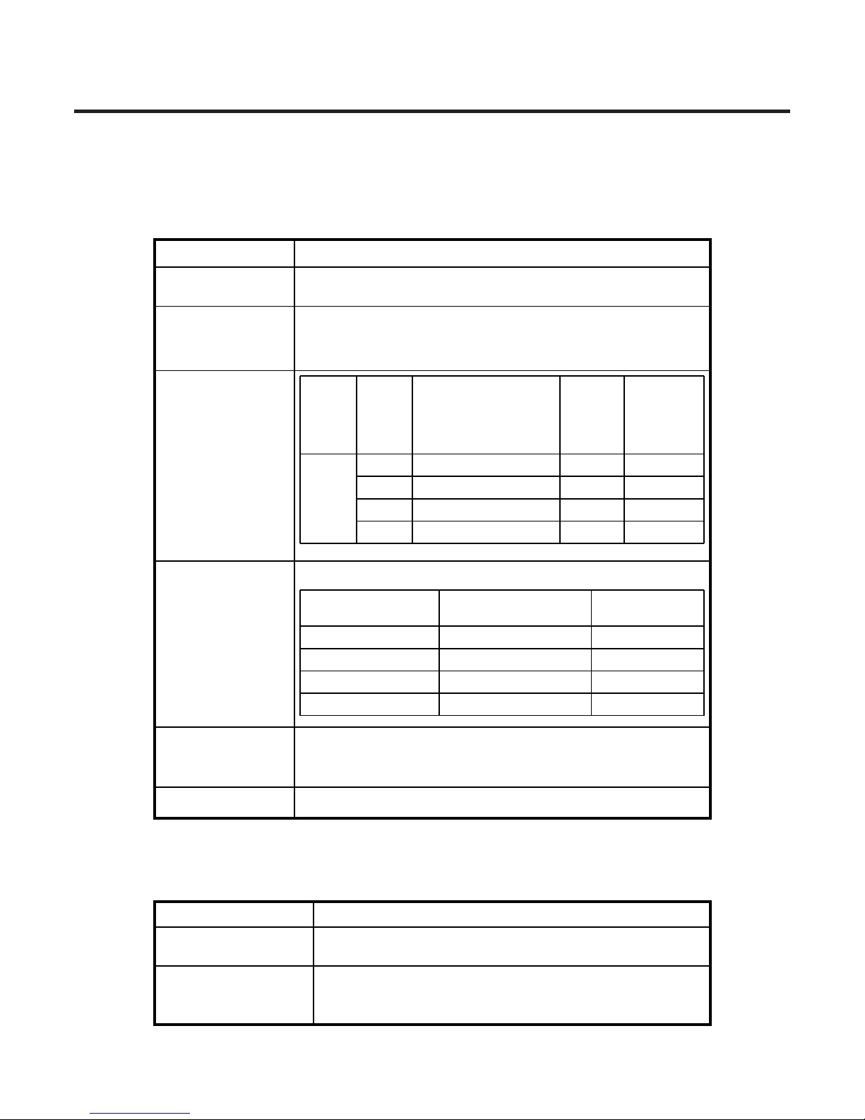
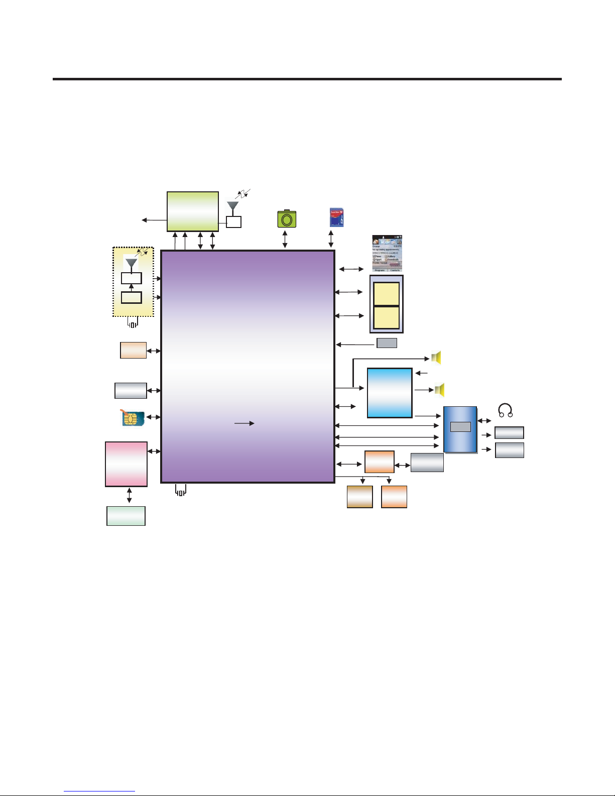
3.1 Functional Block Diagram
[Figure 3.1] Functional Block Diagram
XMM6080
(HSDPA)
CAMERA (3M)
USB2.0
FULL
Micro
SD
Main key
LED
SPEAKER
MOTOR
LCD(WqVGA)
USIM
NAND
DATA
I2C
UART1
RX ADC
TX DAC
UART
VIB_DRV_N
MMC I/F
SDRAM_ DATA
EBU_ ADDR
UART0
D(0:15)
I2S
RF
PAM
FEM
Filter
BT
அ
FM Radio
Audio
AMP
I2C
USIM I/F
Audio Out
SDRAM
1Gbit
NAND
Flash
2Gbit
USB
A(0:24)
D(0:7)
8bit
LCD
32K
26M
26M
FM Audio
FM Audio
Touch
Screen
3-Axis
Sensor
32K
PMB
6821
(PMIC)
I2C
I2C
Battery
QWERTY
KEY
KEY
Encoder
I2C
MIC
Mic In
I2C
MUIC
Receiver
I2C
- 18 -
LGE Internal Use Only Copyright © 2009 LG Electronics. Inc. All right reserved.
Only for training and service purposes
3. BB Circuit Technical brief
GW520 service manual
3.2 Baseband Processor Introduction
[Figure 3.2] Top level block diagram of S-GOLD®3H(PMB8878)

- 19 -
Copyright © 2009 LG Electronics. Inc. All right reserved.
Only for training and service purposes
LGE Internal Use Only
3. BB Circuit Technical brief
GW520 service manual
3.2.1 General description
S-GOLD®3H is a HSDPA/WCDMA/EDGE/GPRS/GSM system in package solution consisting of a
mixed signal baseband IC combined with a 3G coprocessor IC, providing all analog and digital
functionality for a dual mode mobile phone in a single chip.
Both ICs building up the S-GOLD®3H SiP are manufactured in infineon Technologies` 1.35V 90nm
CMOS technology to meet the ever increasing demands of the market for feature rich and high
performance terminals at low costs.
The chip will support the FR, EFR, HR and AMR-NB vocoding.
S-GOLD®3H support multi-slot operation modes HSCSD (up to class 10), GPRS for high speed data
application (up to class 12), EGPRS (up to class 12) and DTM(class11) without additional external
hardware.
3.2.2. Block Description
z Processing core
- ARM926EJ-S 32 bit processor core for controller functions. The ARM926EJ-S includes an MMU,
and the Jazelle Java extension for Java acceleration and a MOVE co-processor to accelerate
Motion Estimation algorithms with based video encoding schemes..
- TEAKLite DSP core
z ARM9-Memory
- 32k Byte Boot ROM on the AHB
- 128k Byte SRAM on the AHB, flexibly usable as program or data RAM
- 32k Byte Instruction Cache
- 32k Byte Data Cache
- 8k Byte Instruction Tightly coupled Memory (I-TCM)
- 8k Byte Data tightly coupled memory (D-TCM)
z TEAKLite®-Memory
- 120k x 16bit Program ROM
- 8k x 16bit Program RAM
- 72k x 16bit Data ROM
- 48k x 16bit Data XRAM
- 5k x 16bit Data YRAM
- Incremental Redundancy(IR) Memory of 35904 words of 16bit

- 20 -
LGE Internal Use Only Copyright © 2009 LG Electronics. Inc. All right reserved.
Only for training and service purposes
3. BB Circuit Technical brief
GW520 service manual
z Shared Memory Block
1.5K x 32bit Shared RAM(dual ported) between controller system and TEAKLite®.
z Controller Bus system
The processor cores and their peripherals are connected by powerful buses.
- Multi-layer AHB for connecting the ARM and the other master capable building blocks with the
internal and external memories and with the peripheral buses.
- An FPI-Bus for connecting GSM peripherals, called hereafter FPI3 bus.
- A controller FPI bus for connecting the low performance controller peripherals such as keypad
etc. called hereafter fPI2 bus.
- FPI2 and FPI3 are connected asynchronously to the AHB buses. 1 DMA controller with
8channels offloads the controller from data transfers.
- 2 AHB Lite buses for connecting multi-media and high performance peripherals, called
AHB_PER1 and AHB_PER2 hereafter. These peripheral buses are connected to the multi-layer
AHB ‘backbone’ by asynchronous, burst capable AHB2AHB bridges which are shared between
accessing masters.
- The DMA controller is enabled to access AHB_PER1 by use of its first master interface and
AHB_PER2 by its second master interface.
z TEAKLite® Bus System
- 1 TEAKLite® data bus for connecting the TEAKLite® data memory and the TEAKLite® peripherals.
Also the data bus is connected into the controller system via shared RAMs to the FPI3 bus.
- 1 TEAKLite® program bus for connecting the TEAKLite® program memory to the TEAKLite®.
z Clock system
The clock system allows widely independent selection of frequencies for the essential parts of the S-
GOLD®3H. Thus power consumption and performance can be optimized for each application.
z Functional Hardware block
- CPU and DSP Timers
- MOVE coprocessor performing motion estimation for video encoding algorithms
(H.263, MPEG-4)
- Programmable PLL with four additional phase shifters for system clock generation
- GSM Timer Module that off-loads the CPU from radio channel timing
- GMSK / 8-PSK Modulator according to GSM-standard 05.04 (5/2000)
· GMSK Modulator: gauss-filter with B*T=0.3
· EDGE Modulator: 8PSK-modulation with linearized GMSK-Pulse-Filter

- 21 -
Copyright © 2009 LG Electronics. Inc. All right reserved.
Only for training and service purposes
LGE Internal Use Only
3. BB Circuit Technical brief
GW520 service manual
- Hardware accelerators for equalizer and channel decoding.
- Incremental Redundancy memory for EDGE class 12 support
- A5/1, A5/2, A5/3 Cipher unit
- GEA1, GEA2, GEA3 Cipher Unit to support GPRS data transmission
- f8 and f9 Cipher unit
- Advanced static and dynamic power management features including TDMA-Frame
synchronous low-power mode and enhanced CPU modes(idle and sleep modes)
- 2D engine for support of image processing and 2D graphics applications. The 2D engine is tightly
coupled to the display interface. The resulting building block consisting of 2D engine and Display
interface is called Display Content Controller (DCC)
- Security crypto box supporting
· AES, DES, 3 DES
· Hash function
· RSA acceleration
· Secret Root Key (e-fuse) and Key Management
· True Random Number Generator
- Sample Rate Converter (SRC) for audio up-sampling
- Comprehensive static and dynamic Power Management
· Various frequency options during operation mode
· 32 kHz clock in standby mode
· Sleep control in standby mode
· RAMs and ROMs in power save mode during standby mode
· Additional leakage current reduction in standby mode possible by switching off for the
TEAKLitre® subsystem.
- Extensive debug support for the controller and the DSP system
· OCDS level 2+ (run control, non-intrusive program flow trace and limited data flow
trace) for ARM
· OCDS level 1+ (run control, limited program flow trace) for the TEAKLite®
· Multi-core debug support
· 4 Monitor pins for important internal signals and most pad signals
· Cerberus debugging unit
- 2 General Purpose Timers with 3 32-bit timers
- Serial number
- A real time clock with alarm functions
- 2 capture/compare units with 16 channels. One channel active during sleep mode.

- 22 -
LGE Internal Use Only Copyright © 2009 LG Electronics. Inc. All right reserved.
Only for training and service purposes
3. BB Circuit Technical brief
GW520 service manual
z 3G Coprocessor Subsystem
- ARM7 TRMI-S
· 240 kByte Instruction RAM
· 64 kByte Data RAM
· 8 kByte Boot ROM
- 20kByte Communication RAM
- HW accelerators for
· Transmit Path
· Inner and Outer Receiver for Release5 incl. HSDPA
3.2.3 RF Interface(T_OUT)
S-Gold® 3H uses this interface to control RF IC and Peripherals.
[Table 3.2.3-1] RF Interface Spec.
T_OUT
Resource Interconnection Description
T_OUT0 TXON_PA PAM Power on
T_OUT1 -
T_OUT2 ANT_SEL1
T_OUT3
T_OUT4 FEM control
T_OUT5 FEM control
T_OUT6 PA_MODE PAM Mode select
T_OUT7 ANT_SEL2
T_OUT8 ANT_SEL3
T_OUT9
T_OUT10
- 23 -
Copyright © 2009 LG Electronics. Inc. All right reserved.
Only for training and service purposes
LGE Internal Use Only
3. BB Circuit Technical brief
GW520 service manual
3.2.4 ADC channel
ADC block is composed of 11 external ADC channel. This block operates charging process and other
related process by reading battery voltage and other analog values.
[Table 3.2.4-1] S-Gold3 ADC channel usage
ADC channel
Resource Interconnection Description
M0 BAT_ID Battery temperature measure
M1 RF_TEMP RF block temperature measure
M2 N.C
M3 N.C
M4 LCD_ID
M5 N.C
M6 N.C
M7 H/W VERSION H/W version detect
M8 VBAT Battery supply voltage measure
M9 N.C
M10 N.C
- 24 -
LGE Internal Use Only Copyright © 2009 LG Electronics. Inc. All right reserved.
Only for training and service purposes
3. BB Circuit Technical brief
GW520 service manual
3.2.5 GPIO map
Over a hundred allowable resources, GW520 is using as follows except dedicated to SIM and Memory.
GW520 GPIO(General Purpose Input/Output) Map, describing application, I/O state, and enable level,
is shown in below table
[Table 3.2.5-1] S-Gold®3H GPIO pin Map
GW520 service manual
Port Function Net Name Description
KEY MATRIX
KP_IN0
NA
KP_IN1
KEY_12C_SCL
KP_IN2
KEY_12C_SDA
KP_IN3
KEY_INT
KP_IN4
TP(NA)
KP_IN5
ACCEL_INT
KP_IN6
NA
KP_OUT0
VGA_PWDN
KP_OUT1
12C3_SCL
KP_OUT2
12C3_SDA
KP_OUT3
LIN_INVERTER
USIF1
USIF1_RXD_MRST
UART_RX UART Data
USIF1_TXD_MTSR
UART_TX UART Data
USIF1_RTS_N
USB_ DAT_VP USB Data
USIF1_CTS_N
USB_SE0_VM USB Data
USIF2
USIF2 _RXD_MRST
TP(NA)
USIF2 _TXD_MTSR
RPWRON_DBB
USIF2_RTS_N
UART_BT_RTS Bluetooth RTS
USIF2_CTS_N
UART_BT_CTS Bluetooth CTS
USIF3
USIF3_RXD_MRST(EINT6)
UART_BT_RX Bluetooth UART Data
USIF3 _TXD_MTSR
UART_BT_TX Bluetooth UART Data
USIF3_SCLK
LIN_MOTOR_EN
CLK
CLK32K
CLK32k For FM Radio, BT CLK32K
CLK26M
TO THE FLIPFLOP(CLK26M)
I2C3_SCL
I2C3_SDA
- 25 -
Copyright © 2009 LG Electronics. Inc. All right reserved.
Only for training and service purposes
LGE Internal Use Only
3. BB Circuit Technical brief
GW520 service manual
CAMERA I/F
CIF_D0
CIF_D0 CAMERA_DATA
CIF_D1
CIF_D1 CAMERA_DATA
CIF_D2
CIF_D2 CAMERA_DATA
CIF_D3
CIF_D3 CAMERA_DATA
CIF_D4
CIF_D4 CAMERA_DATA
CIF_D5
CIF_D5 CAMERA_DATA
CIF_D6
CIF_D6 CAMERA_DATA
CIF_D7
CIF_D7 CAMERA_DATA
CIF_PCLK
CIF_PCLK CAMERA_PCLK
CIF_HSYNC
CIF_HSYNC CAMERA_HSYNC
CIF_VSYNC
CIF_VSYNC CAMERA_VSYNC
CLKOUT2
CIF_MCLK CAMERA_MCLK (26M CLK)
CIF_PD
M_CAM_PD
CIF_RESET
CAM_RESET
LCD I/F
DIF_D0
LCD_DATA(0) LCD_DATA
DIF_D1
LCD_DATA(1) LCD_DATA
DIF_D2
LCD_DATA(2) LCD_DATA
DIF_D3
LCD_DATA(3) LCD_DATA
DIF_D4
LCD_DATA(4) LCD_DATA
DIF_D5
LCD_DATA(5) LCD_DATA
DIF_D6
LCD_DATA(6) LCD_DATA
DIF_D7
LCD_DATA(7) LCD_DATA
DIF_D8
SHIFT_LED
DIF_CS1
LCD_CSn LCD SELECT
DIF_CS2
N.A
DIF_CD
LCD_CD LCD ADDRESS
DIF_WR
LCD_WRn LCD WRITE
DIF_RD
LCD_RDn LCD READ
DIF_HD
CAM_LDO_EN
DIF_VD
LCD_VSYNC
DIF_RESET1
LCD_RESET LCD_RESET
DIF_RESET2
A_RESET 3G reset
I2C
I2C1_SCL
I2C1_SCL For PMIC & AUDIO AMP
I2C1_SDA
I2C1_SDA For PMIC & AUDIO AMP
PM_INT
PM_INT For PMIC
- 26 -
LGE Internal Use Only Copyright © 2009 LG Electronics. Inc. All right reserved.
Only for training and service purposes
3. BB Circuit Technical brief
GW520 service manual
I2C2_SCL
I2C2_SCL FOR CAMERA,TOUCH, 3-AXIS ACCEL……
I2C2_SDA
I2C2_SDA FOR CAMERA,TOUCH, 3-AXIS ACCEL……
SIM I/F
CC_IO
SIM_IO SIM CARD DATA
CC_CLK
SIM_CLK SIM CARD CLOCK
CC_RST
SIM_RST SIM CARD RESET
I2S2
I2S2_CLK0 (GPIO_31)
BT_RESET_N Bluetooth reset
I2S2_CLK1 (GPIO_102)
DBB_BT_INT DBB_WAKEUP
I2S2_RX (GPIO_32)
LIN_PWM_MAG MOTER OPERATION
I2S2_TX (GPIO_33)
BT_INT BT_WAKEUP
I2S2_WA0 (GPIO_34)
TORCH_INT TOUCH INTERRUPT
I2S2_WA1 (GPIO_103)
QWERTY_KEY_EN QWERTY_KEY_ENABLE
External Memory
MMCI1_CMD
MMC_CMD
MMCI1_DAT[0]
MMC_D0
MMCI1_CLK
MMC_CLK
MMC1_DAT[1]
MMC_D1
MMC1_DAT[2]
MMC_D2
MMC1_DAT[3]
MMC_D3
MMCI2_CMD (GPIO_22)
MUIC_INT
MMCI2_DAT[0] (GPIO_107)
LCD_BL_CTRL
MMCI2_CLK (GPIO_108)
FN_LED
IrDA
IrDA_TX (GPIO_110)
USB_OEn For USB
IrDA_RX (GPIO_111)
SLIDE_DETECT Slide on/off detect
I2S1
I2S1_CLK0
BT_PCM_CLK For Bluetooth
I2S1_CLK1
N.A
I2S1_RX
BT_PCM_RX For Bluetooth
I2S1_TX
BT_PCM_TX For Bluetooth
I2S1_WA0
BT_PCM_SYNC For Bluetooth
Audio I/F
EPN1
REC_N For Receiver
EPP1
REC_P For Receiver
EPPA1
EAR_SPK_P For SPK &Headset
EPREF
N.A Reference
- 27 -
Copyright © 2009 LG Electronics. Inc. All right reserved.
Only for training and service purposes
LGE Internal Use Only
3. BB Circuit Technical brief
GW520 service manual
EPPA2
EAR_SPK_N For SPK & Headset
MICN1
MIC_N For Main Mic
MICP1
MIC_P For Main Mic
MICN2
HS_MIC_N For Headset Mic
MICP2
HS_MIC_P For Headset Mic
VMICP
VMIC_P Power for MIC
VMICN
VMIC_GND Ground for MIC
ADC
M0
BAT_ID Battery temperature measure
M1
RF_TEMP RF block temperature measure
M2
N.A
M3
N.A
M4
LCD ID LCD BANDER DETECT
M5
N.A
M6
N.A
M7
N.A
M8
VBAT
M9
TP(N.A)
M10
N.A
Reference
VREFP
VREFN
IREF
GND
JTAG I/F
JTAG0_TDO
TDO
JTAG0_TDI
TDI
JTAG0_TMS
TMS
JTAG0_TCK
TCK
JTAG0_TRST_n
TRST_n
JTAG0_RTCK
RTCK
JTAG1_TDO
A_TDO
JTAG1_TDI
A_TDI
JTAG1_TMS
A_TMS
JTAG1_RTCK
A_RTCK
JTAG1_TRST_n
A_TRSTn
ETM I/F
TRIG_IN
TRIG_IN , 2V62_VIO
MON1
2V62_VIO ETM
MON2
GND ETM
- 28 -
LGE Internal Use Only Copyright © 2009 LG Electronics. Inc. All right reserved.
Only for training and service purposes
3. BB Circuit Technical brief
GW520 service manual
TRACESYNC
TRACESYNC
TRACECLK
TRACECLK
PIPESTAT[2]
PIPESTAT2
PIPESTAT[1]
PIPESTAT1
PIPESTAT[0]
PIPESTAT0
TRACEPKT[0]
TRACEPKT0
TRACEPKT[1]
TRACEPKT1
TRACEPKT[2]
TRACEPKT2
TRACEPKT[3]
TRACEPKT3
TRACEPKT[4]
TRACEPKT4
TRACEPKT[5]
TRACEPKT5
TRACEPKT[6]
TRACEPKT6
TRACEPKT[7]
TRACEPKT7
Memory
MEM_AD[0]
NAND_IO(0)
MEM _AD[1]
NAND_IO(1)
MEM _AD[2]
NAND_IO(2)
MEM _AD[3]
NAND_IO(3)
MEM _AD[4]
NAND_IO(4)
MEM _AD[5]
NAND_IO(5)
MEM _AD[6]
NAND_IO(6)
MEM _AD[7]
NAND_IO(7)
MEM _AD[8]
NAND_IO(8)
MEM _AD[9]
NAND_IO(9)
MEM _AD[10]
NAND_IO(10)
MEM _AD[11]
NAND_IO(11)
MEM _AD[12]
NAND_IO(12)
MEM _AD[13]
NAND_IO(13)
MEM _AD[14]
NAND_IO(14)
MEM _AD[15]
NAND_IO(15)
MEM _WR_n
_WR
MEM _RD_n
_RD
MEM _BC0_n
_BC0
MEM _BC1_n
_BC1
MEM _BC2_n
LDQS
MEM _BC3_n
UDQS
MEM _A[0]
SD-DATA(0) SDRAM DATA
MEM _A[1]
SD_DATA(1)
- 29 -
Copyright © 2009 LG Electronics. Inc. All right reserved.
Only for training and service purposes
LGE Internal Use Only
3. BB Circuit Technical brief
GW520 service manual
MEM _A[2]
SD_DATA(2)
MEM _A[3]
SD_DATA(3)
MEM _A[4]
SD_DATA(4)
MEM _A[5]
SD_DATA(5)
MEM _A[6]
SD_DATA(6)
MEM _A[7]
SD_DATA(7)
MEM _A[8]
SD_DATA(8)
MEM _A[9]
SD_DATA(9)
MEM _A[10]
SD_DATA(10)
MEM _A[11]
SD_DATA(11)
MEM _A[12]
SD_DATA(12)
MEM _A[13]
SD_DATA(13)
MEM _A[14]
SD_DATA(14)
MEM _A[15]
SD_DATA(15)
MEM _A[16]
SD_ADD(0) SDRAM ADDRESS
MEM _A[17]
SD_ADD(1)
MEM _A[18]
SD_ADD(2)
MEM _A[19]
SD_ADD(3)
MEM _A[20]
SD_ADD(4)
MEM _A[21]
SD_ADD(5)
MEM _A[22]
SD_ADD(6)
MEM _A[23]
SD_ADD(7)
MEM _A[24]
SD_ADD(8)
MEM _A[25]
SD_ADD(9)
MEM _A[26]
SD_ADD(10)
MEM_CSA0_N
SD_ADD(11)
MEM_CSA1_N
SD_ADD(12)
MEM_CSA2_N
SD_ADD(13)
MEM_CSA3_N
BA0
MEM _CS0_n
_NAND_CS
MEM _CS1_n
_RAM_CS
MEM _CS2_n
TP(N.A)
MEM _CS3_n
_CS3
MEM _ADV_n
BA1
MEM _RAS_n
_RAS
MEM _CAS_n
_CAS
MEM _WAIT_n
_WAIT
MEM _SDCLK0
SDCLKO For Burst mode
- 30 -
LGE Internal Use Only Copyright © 2009 LG Electronics. Inc. All right reserved.
Only for training and service purposes
3. BB Circuit Technical brief
GW520 service manual
MEM _BFCLK01
BFCLKO For Burst mode
MEM _BFCLK02
SDCLKI For Burst mode
MEM _CKE
CKE
Memory
FCDP_RBn
FCDP
FWP (GPIO_60)
_WP
TDMA I/F
T_OUT0
TXON_PA PAM
T_OUT1
N.A
T_OUT2
ANT_SEL1
T_OUT3 (GPIO_46)
SLIDE_KEY_LED
T_OUT4 (GPIO_47)
_CHG_EOC Charging terminate signal
T_OUT5 (GPIO_48)
MMC_DETECT SD card detect
T_OUT6
PA_MODE PAM
T_OUT7
ANT_SEL2
T_OUT8
ANT_SEL3
T_OUT9 (I2C2_SDA)
TOUCH_SDA
T_OUT10
DSR
T_IN0 (I2C2_SCL)
TOUCH_SCL
T_IN1 (GPIO_55)
CHG_EN Charging enable signal
RF I/F
RF_STR0
2G_EN
RF_STR1
_PPR Charger detect
RF_DATA
2G_DATA
RF_CLK
2G_CLK
GPIO[7]
3G_LD
GPIO[10]
3G_MASTER_ON
GPIO[15]
3G_PA_MODE1
GPIO[16]
ANT_SEL4
GPIO[17]
ANT_SEL5
GPIO[18]
ANT_SEL6
System Port
AFC
TO THE FLIPFLOP(AFC)
CLKOUT0
TO THE PLIPFLOP(26Mhz)
F26M
26MHZ 26M Main Clock
F32K
TO THE CRYSTAL(32.768khz)
to 32k crystal
OSC32K
TO THE CRYSTAL(32.768khz)
to 32k crystal
RESET_N
_RESET
- 31 -
Copyright © 2009 LG Electronics. Inc. All right reserved.
Only for training and service purposes
LGE Internal Use Only
3. BB Circuit Technical brief
GW520 service manual
RSTOUT_N
N.A
RTC_OUT
RTC_OUT
SPCU_RQ_IN1
BT_VCXO_EN
SPCU_RC_OUT0
PM_VCXO_EN
DSP
DSPIN0
CLK32K
DSPOUT1
WDOG
DSPIN1
LIN_PWM_FREQ
GW520 service manual
3.3 Power management IC
3.3.1 General Description
SM-POWER is a highly integrated Power and Battery Management IC for mobile handsets. It has
been specially designed for usage with S-Gold3. Although optimized for usage with the Infineon
SGOLD
baseband device it is suitable for the S-GOLD lite and the E-GOLD+ baseband devices as well.
It also supports the cellular RF devices like SMARTi-DC, SMARTi-DC+, SMARTi-SD and the
Bluemoon Single, Infineon’s single chip solution for Bluetooth. If used with S-GOLD3 it provides all
power supply functions (except for the RF PA) for a complete advanced GSM Edge smart phone
minimizing external device count.
Block Description
• Highly efficient step-down converter for main digital baseband supply including Core, DSP and
memory interface (External Bus Unit).
• Support of S-GOLD standby power-down concept
• Low-drop-out (LDO) regulators for Flash and mobile RAM memory devices
• Voltage independent switching of two SIM cards
• LDO regulators for baseband I/O supply
• LDO regulator for analog mixed-signal section of S-GOLD
• Low-noise LDO regulators for RF devices
• Supply for Bluemoon Single, Infineon’s single chip solution for Bluetooth
• Audio amplifier 8 Ohms for handsfree operation and ringing
 Loading...