


MX-GA77
SERVICE MANUAL
COMPACT COMPONENT SYSTEM
MX-GA77
|
|
|
|
|
CD 1 CD 2 CD 3 |
|
|
|
|
|
|
DISC CHANGE |
|
|
ECO |
|
|
|
|
|
|
|
C O M P A C T C O M P O N E N T S Y S T E M |
M X - G A 7 7 |
|
||
|
R O C K |
|
|
|
D A N C E |
REPEAT |
|
P O P |
|
|
|
H A L L |
PROGRAM |
DUBBING |
CLASSIC |
|
|
|
STADIUM |
RANDOM |
|
|
|
VO |
LU |
|
|
DISPLAY |
|
|
ME |
|
|
|
PHONES |
|
|
D |
|
|
|
|
OUN |
MODE |
|
PRESET |
SET |
|
MP3
SOUND |
|
|
TAPE A /B |
TURBO |
|
|
|
|
DISPLAY MODE |
RDS MODE |
SELECT |
SUBWOOFER LEVEL |
|
|
|
TUNING |
TUNING |
|
|
|
BEEP |
|
|
EJECT |
|
|
EJECT |
|
Area suffix |
||||||||||||
B ------------------------ |
|
|
|
|
|
|
|
|
|
|
|
|
U.K. |
E ---- |
Continental Europe |
||||||||||||
EN ----- |
Northern Europe |
||||||||||||
EV ------- |
Eastern Europe |
||||||||||||
|
|
|
|
|
|
|
|
|
|
|
|
|
|
|
|
|
|
|
|
|
|
|
|
|
|
|
|
SP-MXGA77 |
CA-MXGA77 |
SP-MXGA77 |
Contents
Safety Precautions |
1-2 |
Important for laser produbts |
1-4 |
Preventing static electricity |
1-5 |
Disassembly method |
1-6 |
Wiring connection |
1-19 |
Adjustment method |
1-20 |
Flow of functional operation |
|
until TOC read |
1-24 |
Maintenance of laser pickup |
1-25 |
Replacement of laser pickup |
1-25 |
Trouble shooting |
1-26 |
Description of major ICs |
1-30~44 |
COPYRIGHT  2003 VICTOR COMPANY OF JAPAN, LTD.
No.22083
Jul. 2003

MX-GA77
1.This design of this product contains special hardware and many circuits and components specially for safety purposes. For continued protection, no changes should be made to the original design unless authorized in writing by the manufacturer. Replacement parts must be identical to those used in the original circuits. Services should be performed by qualified personnel only.
2.Alterations of the design or circuitry of the product should not be made. Any design alterations of the product should not be made. Any design alterations or additions will void the manufacturer`s warranty and will further relieve the manufacture of responsibility for personal injury or property damage resulting therefrom.
3.Many electrical and mechanical parts in the products have special safety-related characteristics. These characteristics are often not evident from visual inspection nor can the protection afforded by them necessarily be obtained by using replacement components rated for higher voltage, wattage, etc. Replacement parts which
have these special safety characteristics are identified in the Parts List of Service Manual. Electrical components having such features are identified by shading on the schematics and by ( ) on the Parts List in the Service Manual. The use of a substitute replacement which does not have the same safety characteristics as the recommended replacement parts shown in the Parts List of Service Manual may create shock, fire, or other hazards.
4.The leads in the products are routed and dressed with ties, clamps, tubings, barriers and the like to be separated from live parts, high temperature parts, moving parts and/or sharp edges for the prevention of electric shock and fire hazard. When service is required, the original lead routing and dress should be observed, and it should be confirmed that they have been returned to normal, after re-assembling.
5.Leakage currnet check (Electrical shock hazard testing)
After re-assembling the product, always perform an isolation check on the exposed metal parts of the product (antenna terminals, knobs, metal cabinet, screw heads, headphone jack, control shafts, etc.) to be sure the product is safe to operate without danger of electrical shock.
Do not use a line isolation transformer during this check.
 Plug the AC line cord directly into the AC outlet. Using a "Leakage Current Tester", measure the leakage current from each exposed metal parts of the cabinet, particularly any exposed metal part having a return path to the chassis, to a known good earth ground. Any leakage current must not exceed 0.5mA AC (r.m.s.).
 Alternate check method
Plug the AC line cord directly into the AC outlet. Use an AC voltmeter having, 1,000 ohms per volt or more
sensitivity in the following manner. Connect a 1,500 |
10W resistor paralleled by a 0.15 F AC-type capacitor |
||||||||||||
between an exposed metal part and a known good earth ground. |
|
|
|
|
|
|
|
|
|
AC VOLTMETER |
|||
Measure the AC voltage across the resistor with |
the AC |
|
|
|
|
|
|
|
|
|
(Having 1000 |
||
voltmeter. |
|
|
|
|
|
|
|
|
|
|
|
ohms/volts, |
|
|
|
|
|
|
|
|
|
|
|
|
|||
Move the resistor connection to each exposed metal part, |
|
|
|
|
|
|
|
|
|
or more sensitivity) |
|||
|
|
|
|
|
|
|
|
|
|
||||
particularly any exposed metal part having a return |
path to |
|
|
|
|
|
|
|
|
|
|
||
0.15 F AC TYPE |
|||||||||||||
the chassis, and meausre the AC voltage across the resistor. |
|||||||||||||
|
|
|
|
|
|
|
|
|
|
||||
Now, reverse the plug in the AC outlet and repeat each |
|
|
|
|
|
|
|
|
|
Place this |
|||
|
|
|
|
|
|
|
|
|
|||||
|
|
|
|
|
|
|
|
|
|||||
measurement. Voltage measured any must not exceed 0.75 V |
|
|
|
|
|
|
|
|
|
|
probe on |
||
|
|
|
|
|
|
|
|
|
|
||||
|
|
|
|
|
|
|
|
|
|
each exposed |
|||
AC (r.m.s.). This corresponds to 0.5 mA AC (r.m.s.). |
|
|
1500 |
|
10W |
||||||||
|
|
|
metal part. |
||||||||||
Good earth ground
1.This equipment has been designed and manufactured to meet international safety standards.
2.It is the legal responsibility of the repairer to ensure that these safety standards are maintained.
3.Repairs must be made in accordance with the relevant safety standards.
4.It is essential that safety critical components are replaced by approved parts.
5.If mains voltage selector is provided, check setting for local voltage.
!
Burrs formed during molding may be left over on some parts of the chassis. Therefore, pay attention to such burrs in the case of preforming repair of this system.
In regard with component parts appearing on the silk-screen printed side (parts side) of the PWB diagrams, the parts that are printed over with black such as the resistor ( ), diode (
  ) and ICP (
  ) or identified by the " " mark nearby are critical for safety.
(This regulation does not correspond to J and C version.)
1-2

|
|
|
|
|
MA-GA77 |
|
|
|
|
|
|
|
|
|
|
|
|
|
|
|
|
|
|
|
(U.K only) |
|
|
|
|
|
|
|||
|
|
|
|
|
||
1. This |
design |
of this product contains special hardware and many circuits and components specially |
||||
|
for |
safety |
purposes. For continued protection, no changes should be made to the original |
|||
|
design unless authorized in writing by the manufacturer. Replacement parts must be identical to |
|||||
|
those used |
in the original circuits. |
||||
2.Any unauthorised design alterations or additions will void the manufacturer's guarantee ; furthermore the manufacturer cannot accept responsibility for personal injury or property damage resulting therefrom.
3.Essential safety critical components are identified by (  ) on the Parts List and by shading on the schematics, and must never be replaced by parts other than those listed in the manual. Please note
however that many electrical and mechanical parts in the product have special safety related characteristics. These characteristics are often not evident from visual inspection. Parts other than specified by the manufacturer may not have the same safety characteristics as the recommended replacement parts shown in the Parts List of the Service Manual and may create shock, fire, or other hazards.
4. The |
leads |
in the products are routed and dressed with ties, clamps, tubings, barriers and the |
|||||||
|
like |
to be |
separated from live parts, high |
temperature parts, moving |
parts and/or |
sharp edges |
|||
|
for |
the prevention |
of electric |
shock and fire |
hazard. When service is |
required, the |
original lead |
||
|
routing and |
dress |
should be |
observed, and it should be confirmed that they have been returned |
|||||
|
to normal, |
after re-assembling. |
|
|
|
||||
|
|
|
|
|
|
|
|
|
|
|
|
|
|
|
|
|
|
|
|
1. Service should be performed by qualified personnel only. |
|
|
|
|
|||
2. This equipment has been designed and manufactured to |
meet international safety |
standards. |
|||||
3. It |
is the |
legal |
responsibility of the repairer to ensure that these safety |
standards |
are maintained. |
||
4. Repairs |
must |
be made in accordance with the relevant |
safety |
standards. |
|
||
5. It |
is essential |
that safety critical components are replaced by |
approved |
parts. |
|
||
6. If |
mains |
voltage selector is provided, check setting for |
local voltage. |
|
|
||
! |
Burrs formed during molding may be left over on some parts of the chassis. Therefore, |
|
pay attention to such burrs in the case of preforming repair of this system. |
1-3
MX-GA77
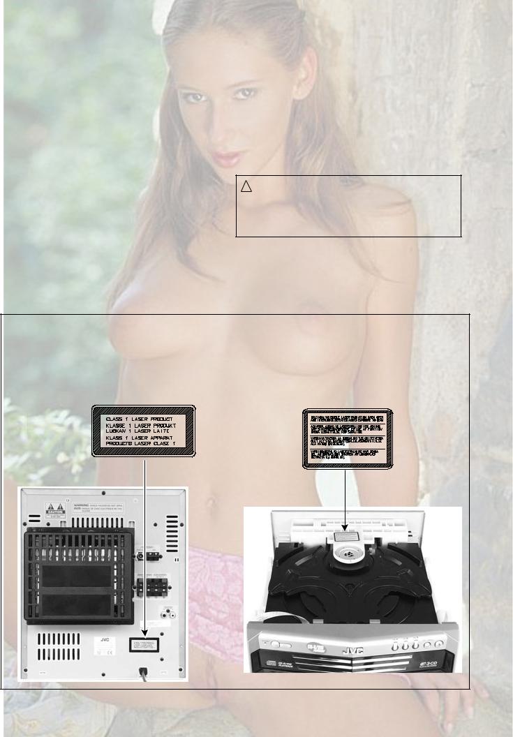
Important for laser products
1.CLASS 1 LASER PRODUCT
2.DANGER : Invisible laser radiation when open and inter lock failed or defeated. Avoid direct exposure to beam.
3.CAUTION : There are no serviceable parts inside the Laser Unit. Do not disassemble the Laser Unit. Replace the complete Laser Unit if it malfunctions.
4.CAUTION : The compact disc player uses invisible laserradiation and is equipped with safety switches whichprevent emission of radiation when the drawer is open and the safety interlocks have failed or are de feated. It is dangerous to defeat the safety switches.
5.CAUTION : If safety switches malfunction, the laser is able
to function.
6.CAUTION : Use of controls, adjustments or performance of procedures other than those specified herein may result in hazardous radiation exposure.
! CAUTION Please use enough caution not to see the beam directly or touch it
in case of an adjustment or operation check.
REPRODUCTION AND POSITION OF LABELS
CLASS 1 |
|
LASER PRODUCT |
WARNING LABEL |
|
1-4

MA-GA77
Preventing static electricity
1. Grounding to prevent damage by static electricity
Electrostatic discharge (ESD), which occurs when static electricity stored in the body, fabric, etc. is discharged, can destroy the laser diode in the traverse unit (optical pickup). Take care to prevent this when performing repairs.
2. About the earth processing for the destruction prevention by static electricity
In the equipment which uses optical pick-up (laser diode), optical pick-up is destroyed by the static electricity of the work environment.
Be careful to use proper grounding in the area where repairs are being performed.
2-1 Ground the workbench
Ground the workbench by laying conductive material (such as a conductive sheet) or an iron plate over it before placing the traverse unit (optical pickup) on it.
2-2 Ground yourself
Use an anti-static wrist strap to release any static electricity built up in your body.
(caption)
Anti-static wrist strap
Conductive material (conductive sheet) or iron plate
3. Handling the optical pickup
1. In order to maintain quality during transport and before installation, both sides of the laser diode on the replacement optical pickup are shorted. After replacement, return the shorted parts to their original condition. (Refer to the text.)
2.Do not use a tester to check the condition of the laser diode in the optical pickup. The tester's internal power source can easily destroy the laser diode.
4. Handling the traverse unit (optical pickup)
1.Do not subject the traverse unit (optical pickup) to strong shocks, as it is a sensitive, complex unit.
2.Cut off the shorted part of the flexible cable using nippers, etc. after replacing the optical pickup. For specific details, refer to the replacement procedure in the text. Remove the anti-static pin when replacing the traverse unit. Be careful not to take too long a time when attaching it to the connector.
3.Handle the flexible cable carefully as it may break when subjected to strong force.
4.It is not possible to adjust the semi-fixed resistor that adjusts the laser power. Do not turn it
Attention when CD mechanism assembly is decomposed
*Please refer to "Disassembly method" in the text for pick-up and how to detach the CD mechanism assembly.
CD changer unit
1.Remove the CD changer unit.
2.Remove the CD changer mechanism.
3.Solder is put up before the card wire is removed from the pickup unit connector on the CD mechanism assembly.
(When the card wire is removed without putting up solder, the CD pick-up assembly might destroy.)
4.Please remove solder after connecting the card wire with the pickup unit connector when you install picking up in the substrate.
Card wire
Picup unit connector
Soldering
CD changer mechanism
Fig.1
Card wire
Picup unit connector
Fig.2
1-5

MX-GA77
Disassembly method
 Removing the metal cover (See Fig.1)
1.Remove the three screws A attaching the metal cover on the back of the body.
2.Remove the six screws B attaching the metal cover on both sides of the body.
3.Remove the metal cover from the body by lifting the rear part of the cover.
ONE POINT
 How to eject the CD tray manually
(see fig.2)
Turn the loading pulley gear at the bottom of the CD changer unit as shown in Fig.2 and draw the CD tray toward the front.
Metal cover
A
B
(both sides)
Fig.1
Loading pulley gear
(See <CD changer unit>fig.1)
 Removing the CD tray fitting
(See Fig. 3)
Prior to performing the following procedure, eject the CD tray.
1.After drawing the lower part of the tray fitting toward the front, remove the five claws. Then, while moving the tray fitting upward, remove it.
Fig.2
Joint
CD tray fitting
 Removing the CD changer unit
(See Fig.4 to 7)
 Prior to performing the following procedure, remove the metal cover and CD tray fitting.
1.Remove the card wire attached to CD changer unit on the adhesion tape.
2.Disconnect the card wire from the connector CW105 on the CD board.
3.Disconnect the harness from the connector CW104 on the main board.
4.Remove the two screws C attaching the CD changer unit to the rear panel.
5.Remove the two screws D attaching the CD changer unit to both sides of the front panel assembly.
6.Draw the CD changer unit upward from behind while pulling the rear panel outward.
1-6
Claw
Fig.3
Card wire
CD changer unit
Adhesion tape
Fig.4

MA-GA77
CW105 |
CD board |
C |
Rear panel
CD changer unit
CW104
Main board
Fig.5
 Removing the front panel assembly
(See Fig.8 to 10)
 Prior to performing the following procedure, remove the metal cover and CD changer unit.
1.Disconnect the card wire from the connector CW101 on the main board.
2.Disconnect the harness from the connector CW108, CW109 and CW110 on the main board.
3.Remove the screw E fixiing the lug wire.
4.Remove the two screws F attaching the front panel assembly to both sides of the body.
5.Remove the screw G attaching the main board to the front panel assembly.
6.Remove the screw H attaching the front panel assembly to bottom of the body.
7.Release the two joints1 and two joints2, and detach the front panel assembly toward the front.
|
|
|
|
Fig.6 |
|
|
|
Front panel |
|
|
|
|
|
|
|
assembly |
|
CD changer unit |
|
|
|||
D |
|
|
|
|
|
|
|
(both sides) |
|
|
|
|
|
|
|
|
|
|
|
Fig.7 |
|
Rear panel |
|
|
|
|
|
|
|||
|
|
|
|
|
|
||
Front panel |
|
|
|
|
|
Main board |
|
assembly |
CW101 |
|
|
||||
|
|
|
|||||
|
|
CW109 |
|
ACW1 |
|||
|
|
|
CW110 |
|
|||
|
|
|
|
CW108 |
|
ACW2 |
|
|
|
|
|
|
|||
|
|
|
|
|
|
||
|
|
|
|
|
|
|
|
|
|
|
|
|
|
|
|
|
|
|
|
|
|
|
|
|
Amp. board |
Joint1 |
|
(both sides) |
E(fixing the lug wire) |
F |
|
(both sides) |
Fig.8 |
|
|
|
Front panel |
|
assembly |
Main board
G
Joint1 (both sides)
Fig.9 |
F |
(both sides) |
1-7
MX-GA77
 Removing the heat sink & amp. board (See Fig.8, 11 and 12)
 Prior to performing the following procedure, remove the metal cover and CD changer unit.
1.Disconnect the card wire from the connector ACW1 and the harness from the connector ACW2 on the amp. board.
2.Remove the four screws I attaching the heat sink cover to the rear panel. Remove the heat sink cover.
3.Remove the four screws J attaching the heat sink and two screws K attaching the speaker terminal to the rear panel.
4.After moving the heat sink upward, remove the claws. Then pull out the heat sink & amp. board inward.
Joint2
H
Fig.10
I
Heat sink cover
I
 Removing the tuner board
(See Fig.12 and 13)
 Prior to performing the following procedure, remove the metal cover.
1.Disconnect the card wire from the connector CON01 on the tuner board.
2.Remove the two screws L attaching the tuner board to the rear panel.
Fig.11
J
Claws
Heat sink
|
Removing the rear panel |
(See Fig.12) |
|
 Prior to performing the following procedure, remove the metal cover, CD changer unit, heat sink & amp. board and tuner board.
1.Remove the three screws M and three screws N attaching the rear panel.
1-8
J
N
Fig.12
CON01
Main board
Fig.13
(Bottom side)
Rear panel
Rear panel
L
K
Speaker terminal
M
Rear panel
Tuner board
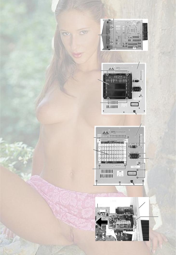
 Removing the main board (See Fig. 14)
 Prior to performing the following procedure, remove the metal cover, CD changer unit and rear panel.
CW108
1. Disconnect the card wire from the connector CW101,
and the harness from the connector CW108, Fuse board CW109, CW110 and CW11, and the power cord
from the connector PW103 on the main board.
PCW1
2.Disconnect the harness from the connector PCW1 on the fuse board.
MA-GA77
CW101
CW109
CW110
Main board
Heat sink
PW103
3.Remove the screw G attaching the main board to the front panel assembly. (See Fig.9)
4.Remove the two screws O attaching the heat sink to the bottom chassis.
 Removing the power cord (See Fig. 14)
 Prior to performing the following procedure, remove the metal cover, CD changer unit and rear panel.
1.Disconnect the power cord from the connector PW103 on the main board and pull up the power cord stopper upward.
 Removing the power ICs
(See Fig.15 and 16)
 Prior to performing the following procedure, remove the metal cover, CD changer unit and heat sink & amp. board.
1.Unsolder the power ICs solder points.
2.Remove the four screws P attaching the power ICs to the heat sink.
 Removing the power transformer
(See Fig .17)
 Prior to performing the following procedure, remove the metal cover, CD changer unit and heat sink & amp. board.
1.Disconnect the harness from the connector PW102 on the power supply board.
2.Disconnect the harness from the connector PCW1 on the fuse board.
3.Remove the four screws Q attaching the power transformer on the bottom chassis.
PW102 |
CW11 |
Bottom chassis |
O |
|
Power cord |
Power supply board |
Power cord stopper |
|
Fig.14
Power ICs solder point
 Heat sink
Amp. board (reverse side)
Fig.15
P |
Heat sink |
|
Amp. board
|
Fig.16 |
|
Power transformer |
|
Fuse board |
|
PCW1 |
Q |
Power supply board |
Bottom |
PW102 |
chassis |
Fig.17
1-9

MX-GA77
<Front panel assembly>
 Prior to performing the following procedure, remove the front panel assembly.
|
|
Removing the CD switch board (See Fig.1) |
B |
|
1. |
||||
Disconnect the card wire from the connector UCW03 |
||||
|
||||
on the CD switch board.
2.Remove the five screws A attaching the CD switch board.
|
|
Removing the front board |
B |
|
|
|
|||
|
|
Connector |
||
|
|
(See Fig.1 and 2) |
||
|
|
Mecha. |
||
1. |
Pull out the sound mode knob, volume knob, and |
|||
board |
||||
|
|
preset knob from the front side of front panel |
|
|
|
|
assembly. |
|
|
2. |
Disconnect the card wire from the connector UCW02 |
|
||
|
|
on the front board and the connector on the mecha. |
|
|
|
|
board. |
|
|
3. |
Remove the fifteen screws B attaching the front |
|
||
|
|
board. |
|
|
4. |
Disconnect the card wire from the connector UCW01 |
|
||
|
|
on the front board. |
|
|
|
Front panel assembly (inner side) |
A |
CD switch board |
|
UCW03 |
|
Front board |
|
UCW02 |
|
UCW01 |
Fig.1
Sound mode knob
Volume knob
Preset knob
 Removing the headphone jack board (See Fig.3)
 Prior to performing the following procedure remove the front board.
1. |
You can pull out the headphone jack board. |
Fig.2 |
|
Front panel assembly (inner side)
 Removing the cassette mechanism assembly (See Fig.3)
1.Disconnect the card wire from the connector on the mecha. board.
2.Remove the six screws C attaching the cassette mechanism assembly.
|
Headphone |
Connector |
jack board |
|
|
C |
|
Mecha. |
C |
board |
|
C |
Cassette mechanism |
(fixing the lug wire) |
assembly |
Fig.3
1-10
<CD changer unit>
 Prior to performing the following procedure, remove the CD changer unit.
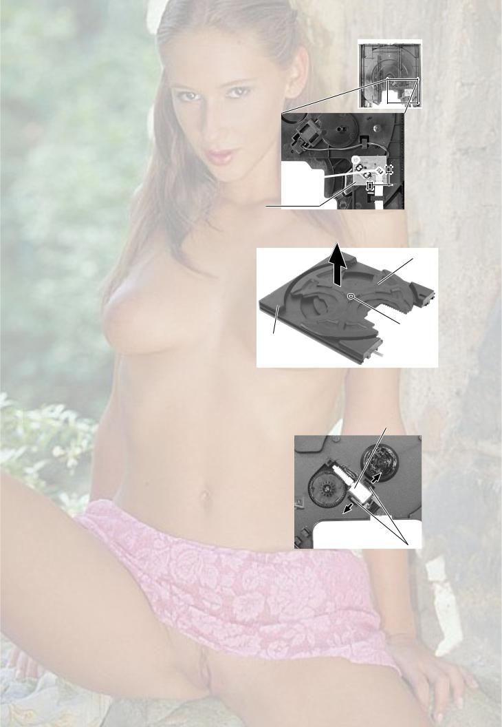
 Removing the CD tray (See Fig.1 and 2)
1.Turn the black loading pulley gear on the under side of the CD changer unit in the direction of the arrow and draw the CD tray toward the front until it stops.
2.Disconnect the card wire from connector CW103 on the CD board.
3.Push down the two tray stoppers marked a and pull out the CD tray.
Loading pulley gear
MA-GA77
CD changer uint (reverse side)
CD tray
CD board

 CW103
CW103
Fig.1
 Reinstall the CD tray (See Fig.3 and 4)
1.Align the gear-cam with the gear-tray as shown fig.3, then mount the CD tray.
2.When assembling the CD tray, take extreme care not engage with gear - synchro.
Gear-cam
Gear-tray
a (Tray stopper)
CD tray
a
(Tray stopper)
CW103
(on the CD board)
Fig.2
Gear-convert |
Gear-cam |
Gear-synchro |
timing point |
||
|
Gear-tray |
|
|
|
CD tray |
Gear-convert |
Gear-tray |
|
|
Fig.3 |
Fig.4 |
1-11
MX-GA77
 Removing the sensor board (See Fig.5)
 Prior to performing the following procedure, remove the CD tray.
1.Remove the screw A attaching the sensor board on the CD tray.
2.Remove the sensor board releasing the two tabs a.
3.Disconnect the harness from the connector CW1 on the sensor board.
 Removing the turn tray motor
(See Fig.6 and 7)
 Prior to performing the following procedure, remove the CD tray and sensor board.
1.Remove the screw B attaching the turn tray. Detach the turn tray from the base tray.
2.Pull outward the tab b attaching the turn tray motor on the base tray and detach the turn tray motor.
Introductory notes:
Base tray + Turn tray = CD tray
CD tray (reverse side)
 A
A
CW1 
Tab a
Sensor board
Fig.5
Turn tray
B
Base tray
Fig.6
Turn tray motor
Base tray (upper side)
Tab b
Fig.7
1-12

 Removing the belt, the CD board and the switch board (See Fig.8 and 9)
 Prior to performing the following procedure, remove the CD tray.
1.Detach the belt from the pulley on the upper side of the CD changer unit (Do not stain the belt with grease).
2.Disconnect the card wire from the pickup unit connector on the under side of the CD changer unit.
Attention : Solder is put up before the card wire is removed from the pick-up unit connector on the CD mechanism assembly.
(When the card wire is removed without putting up solder, the CD pick-up unit assembly might destroy.)
3.Disconnect the motor wire harness from connector on the CD board.
4.Remove the screw C attaching the switch board and release the two tabs e attaching the switch board outward and detach the switch board.
5.Remove the two screws D attaching the CD board. First release the two tabs f and two tabs g attaching the motor, then release the CD board.

 If the tabs f and g are hard to release, it is recommendable to unsolder the two soldered parts on the motor terminal of the CD board.
MA-GA77
Belt
CD changer unit
Fig.8
D CD board
Tabs g
Soldered parts
Tabs e

 Motor
Motor
 Tabs f
C
Switch board
CW3
CD mechanism board motor connecter
Pickup unit connector
Card wire
Soldering |
Picup unit |
|
connector |
Fig.9
1-13
MX-GA77
 Removing the CD mechanism holder assembly (mechanism included)
(See Fig.10 to 13)
1.Disconnect the harness from connector on the CD mechanism board in the CD mechanism assembly on the under side of the CD changer unit. Disconnect the card wire from the pickup unit connector.
Attention : Solder is put up before the card wire is removed from the pick-up unit connector on the CD mechanism assembly. (Refer to Fig.9)
(When the card wire is removed without putting up solder, the CD pick-up unit assembly might destroy.)
2.Remove the screw E attaching the shaft on the right side of the CD mechanism holder assembly. Pull outward the stopper fixing the shaft on the left side and remove the CD mechanism holder assembly from behind in the direction of the arrow y.
3.Turn the CD mechanism holder assembly half around the lift up slide shaft h of the CD mechanism holder assembly until the turn table is reversed, and pull out the CD mechanism holder assembly.
Motor connecter
CD changer unit
CD mechanism holder assembly Pickup unit connector
Fig.10
E
Stopper
CD mechanism holder assembly
Fig.11
Lift up slide shaft n
Lift up slide shaft
y
CD mechanism holder assembly |
CD mechanism holder assembly |
|
|
Fig.13 |
Fig.12 |
1-14
<CD mechanism section>
•Removing the CD mechanism holder from the CD chager unit.
(Refer to "Removing the CD mechanism holder assembly" )
|
Removing the pickup unit |
(See Fig.1) |
|
1.Removing the cut washer on the feed gear sleeve and pull out the feed gear.
2.Remove the two screws A fixing the pickup shaft.
3.Removing the pickup unit.
|
Removing the motor board |
(See Fig.2) |
|
1.Unsolder the motor terminal on the motor board.
2.Remove the moter board.
|
Removing the feed motor |
(See Fig.1) |
|
Remove the two motor fixing screws at B and removing the feed motor.
 Removing the spindle motor
The spindle motor cannot be removed as a single unit.
When removing the spindle motor, change the chasis and turntable together as aunit.
A
Motor board
Spindle motor
MA-GA77
Shutter
Pickup unit Shaft
A
|
|
|
Cut washer |
||
|
|
|
|||
B |
|||||
Fig.1 |
Feed Gear |
||||
|
|
|
|||
Unsolder Feed motor
Unsolder
Fig.2
1-15

MX-GA77
<Cassette mechanism section>
 Prior to performing the following procedure, remove the cassette mechanism assembly.
 Removing the R/P head.
(See Fig.1 and 2)
1.Remove the screw A on the right side of the R/P head.
2.Remove the screw B on the left side of the R/P head.
|
Remove the erase head. |
(See Fig.1) |
|
1. Remove the screw C fixing the erase head.
R/P Head
 Pinch roller
E. Head |
C B A |
|
Fig.1
B A
|
|
Spring |
R/P Head |
|
|
|
Fig.2 |
|
Remove the pinch roller. |
(See Fig.3) |
Pinch roller |
|
stopper |
||
|
1. Pull out the pinch roller stopper.
2. Pull out the pinch roller.
Pinch roller
Fig.3
1-16

|
Removing the motor |
(See Fig. 4 to 6) |
|
1.Slide the plastic cover in the direction of the arrow, and remove the three claws. Then remove the plastic cover.
2.Remove the two screws D fixing the motor.
Be careful to grease's splash when the drive belt comes off.
3.Unsolder the motor terminal.
 Removing the mechanism board
(See Fig. 5)
1.Unsolder the four solder parts a and the four solder parts b.
2.Remove the two screws E attaching the mecha. board.
 Removing the flywheel
(See Fig. 7 and 9)
1.Remove the cut-washer at c from the capstan shaft, then remove the flywheel.
When reassembling the flywheel, be sure to use new washers as they cannot be reused.
MA-GA77
D
Plastic cover
Claw
Fig.4
Motor terminal
Solder |
Solder |
E part b |
part a E Mecha. board |
Solder
part a
Motor |
Drive belt |
Fig.5
Drive belt
Motor
Drive belt
Flywheel
Fig.6
FR belt
Fig.8
c
Sleeve
Washer
FR belt
 Capstan
washer
Fig.9
Fig.7
1-17
MX-GA77
< Speaker section > |
A |
A |
|
|
It is exchange in a unit. |
||
|
|
|
|
|
Please do not decompose as much as possible. |
|
|
|
Removing the side panel |
(See Fig. 1) |
|
|
|
||
|
|
||
1.Remove the five screws A attaching the side panel and remove the side panel.
A
 Removing the side speaker
(See Fig. 2 and 3)
 Prior to performing the following procedure, remove the side panel.
1.Remove the four screws B attaching the side speaker.
2.Pull out the side speaker and remove the speaker cord from the speaker terminal.
Side panel
Fig.1
B
Side speaker
Fig.2
Side speaker
Speaker terminal
Fig.3
1-18

3809-001211
3809-001434
CON01
|
|
|
|
Tuner board |
|
9 |
|
||
|
|
|
|
|
0 |
|
|||
|
|
CW101 |
|
|
|
CW104 CW103 |
|
||
|
|
CW109 |
CW110 |
|
|
|
|||
|
|
|
|
|
CW105 |
|
|||
|
|
|
|
|
|
|
|
|
|
|
|
|
CW111 |
Main board |
|
||||
|
|
|
|
|
|
CW108 |
PW103 |
|
|
|
|
|
|
|
|
|
|
|
|
0 |
|
|
|
|
CW107 |
|
CW11 |
|
|
|
|
|
|
9 |
|
|
|
||
|
|
|
|
|
|
CW106 |
|
||
2 |
9 |
|
|
|
|
|
|
||
|
|
|
0 |
|
|
9 |
|
||
|
|
|
|
|
|
|
|
||
|
|
|
|
|
|
|
|
0 |
|
2 |
|
|
|
|
|
0 |
9 |
0 |
|
|
|
|
|
|
|
|
|||
|
|
|
|
|
|
|
|
||
|
|
|
|
|
|
|
|
9 |
|
|
|
00022A- |
|
CW01B |
|
|
|
|
|
|
|
|
|
|
0 |
AH39-00247A |
|
||
|
|
|
|
|
|
|
|||
|
|
AH39 |
|
|
|
9 |
|
||
|
|
|
Headphone J.board |
|
|||||
|
|
|
|
|
|||||
|
0 |
9 |
|
0 |
|
|
|
|
|
|
|
|
|
|
|
|
|
||
|
|
9 |
0 |
|
9 |
|
|
|
|
AH39-20002D |
|
8 |
8 |
2 |
|
|
|
|
|
|
|
|
|
|
|
2 |
|
|
|
|
|
|
|
|
0 |
|
0 |
|
|
|
|
|
|
|
|
9 |
9 |
0 |
|
|
|
|
|
|
|
|
2 |
|
8 |
|
|
|
|
|
|
|
|
|
|
9
0
3809-001259
0
9
 9
9  2 0
2 0
8
19-1
3809-001413 |
|
|
Wiring |
CD switch board |
|
|
|
AH39-00295A |
|
|
|
UCW03 |
ACW2 |
Amp. board |
connection |
|
|
||
3809-001228 |
ACW1 |
|
|
|
|
|
|
Front board |
0 |
|
|
|
9 |
|
|
UCW02 |
|
|
|
UCW04 |
|
|
|
UCW01 |
|
|
|
UCW05 |
|
|
|
9
0
Power transformer
AH39-00466A
0 9
CW3
CW101
CW104
CW107
CW106  CW105
CW105
CD board |
9 |
0
AH39-00060A
AH38-12001A
CW102
CW103
PCW1
AH39-00338A
3809-001121
AH39-20561P
CW2
CW3 |
CW1 |
|
|
|
AAN1 |
|
|
2 |
|
001034-3809 |
|
0 |
|
2 |
0 |
||
|
PW102
0
9
CD mechanism
0 |
9 |
8 |
7 |
6 |
5 |
4 |
3 |
2 |
1 |
codesColor |
|
|
|
9 |
0 |
|
|
|
|
|
|
|
|
|
|
|
|
|
|
|
|
|
|
|
|
Black |
White |
Gray |
Violet |
Blue |
Green |
Yellow |
Orange |
Red |
Brown |
.below shown are |
-MA |
|
|
|
|
|
|
|
|
|
|
|
GA77 |

MX-GA77
Adjustment method
1. Tuner
* Adjustment Location of Tuner PCB
ITEAM |
AM(MW) OSC |
AM(MW) RF |
|
|
|||
Adjustment |
Adjustment |
|
|
||||
|
|
|
|
|
|
|
|
|
|
|
|
|
|
|
|
Received FREQ. |
522~1629 KHz |
594 KHz |
|
|
|||
|
|
|
|
|
|
|
|
Adjustment |
MO |
|
MA |
|
|
||
point |
|
|
|
||||
|
|
|
|
|
|
|
|
|
|
|
|
|
|
|
|
Output |
1~7.0 0.5V |
Maximum |
|
|
|||
Output(Fig.1) |
|
|
|||||
|
|
|
|
|
|||
|
|
|
|
|
|
|
|
|
|
|
|
|
|
|
|
|
|
MAIN |
VT |
GND |
|
|
TESTER |
|
|
PCB |
|
|
|
|
|
|
|
|
|
|
|
|
|
|
|
|
|
|
|
|
|
Fig.1 OSC Voltage
1-20
FM THD Adjustment
SSG FREQ. |
98 MHz |
Adjustment
point FM DETECTOR COIL (FM DET)
Output |
60 dB |
Minumum Distortion (0.4% below) (Fig.2)
MA-GA77
Output |
FM |
|
|
Antenna SET |
|
||
GND |
|
||
Terminal |
|
||
|
Oscilloscope |
||
FM S.S.G |
Input |
||
|
|||
|
Speaker |
|
|
|
Terminal |
Input |
|
|
output |
||
|
Distortion Meter |
||
Fig.2 IF CENTER and THD Adjustment
FM Search Level Adjustment
SSG FREQ. |
98 MHz |
|
|
|
|
Adjustment |
BEACON |
|
point |
||
SENSITIVITY |
||
(SVR1) |
SEMI-VR(10K ) |
|
|
|
|
Output |
28 dB( 2dB) |
|
|
|
Adjust SVR1 (Fig.3)
*Adjust FM S.S.G level to 28dB
AM(MW) I.F Adjustment
SSG FREQ. |
450 kHz |
|
|
Frequency |
522 kHz |
|
|
Adjustment |
AM IF |
point |
|
|
|
Maximum output (Fig.4)
|
28 dB |
FM Antenna |
|
|
SET |
FM S.S.G |
GND |
FM IN |
|
20 k
Fig.3 FM Auto Search Level Adjustment
|
60cm |
|
|
AM IF |
|
OUTPUT |
AM ANT |
|
IN |
||
|
||
AM SSG |
Speaker Terminal |
|
450KHZ |
|
|
INPUT |
OUTPUT |
VTVM Oscilloscope
Fig.4 AM I.F Adjustment
1-21

MX-GA77
2. Cassette Deck
 To adjust tape speed
Notes
1)Measuring tape:
i) VT-712/MTT-111(or equivalent)
(Tapes recorded with 3kHz)
ii) AC-225/MTT-5512(or equivalent)
2)Connect the cassette deck to the frequency counter as in fig.1.
Cassette Deck |
Frequency Counter |
SPK OUT 
output
Fig.1
Step |
Item |
Pre-Setup |
|
Pre-Setup |
To Adjust |
Standard |
Remark |
Condition |
|
||||||
|
|
|
|
|
|
|
|
|
|
|
|
|
|
|
|
1 |
NOR |
SPK OUT |
1) |
Deck 1:VT-712 |
Turn VSR1 to |
3KHz |
1% |
|
SPEED |
(connected to the |
2) |
Press PLAY |
left and right |
|
range |
|
Control |
frequency counter) |
|
SW button |
(FRONT PCB) |
|
|
|
|
|
3) |
Deck 2:Same |
|
|
|
|
|
|
|
as above |
|
|
|
|
|
|
|
|
|
|
|
 To adjust plabyback level/REC
Notes
1)Before the actual adjustment, clean the play/recording head.
2)Measuring tape :
i)VT-703/MTT-114N(or equivalent 10kHz AZIMUTH control)
ii)AC-225/MTT-5512(or equivalent)
3)The cassette deck is connections as shown in fig.2.
MAIN PCB |
VTVM |
Oscilloscope |
|
|
|||
SPK OUT |
|
|
|
(GND) |
In |
Out |
|
|
|
||
|
Fig.2 |
|
|
1. Adjust Deck 1 Play Level
Step |
Item |
Pre-Setup |
Pre-Setup |
To Adjust |
Standard |
Remark |
|
Condition |
|||||||
|
|
|
|
|
|
||
|
|
|
|
|
|
|
|
1 |
AZIMUTH |
SPK OUT |
After putting VT-703 |
Turn the control |
Max output |
After |
|
|
|
(VTVM is |
into Deck 1 |
screw to as |
and same phase |
adjustment |
|
|
|
- Press FWD PLAY |
shownin Fig.3. |
(both channels) |
secure it with |
||
|
|
connected to |
|||||
|
|
button. |
|
|
REGION |
||
|
|
the scope) |
|
|
|||
|
|
|
|
|
LOCK. |
||
|
|
|
|
|
|
||
|
|
|
|
|
|
|
1-22
MA-GA77
2. Adjust Deck 2 Play Level/REC BIAS
Step |
Item |
Pre-Setup |
Pre-Setup |
To Adjust |
Standard |
Remark |
|
Condition |
|||||||
|
|
|
|
|
|
||
|
|
|
|
|
|
|
|
1 |
AZIMUTH |
SPK OUT |
After putting VT-703 |
Turn the control |
Max output |
After |
|
|
|
(VTVM is |
into Deck 2 |
screw to as |
and same phase |
adjustment |
|
|
|
connected to |
1)Press FWD PLAY |
shown in Fig.3. |
(both channels) |
secure it with |
|
|
|
the scope) |
button. |
|
|
REGION |
|
|
|
|
|
|
|
LOCK. |
|
|
|
|
|
|
|
|
|
2 |
Recording |
Fig.4 |
After putting AC-225 |
Turn JSR2L, |
CHECK TO |
|
|
|
Bias |
|
into Deck 2 |
JSR2R to the |
7mV( 0.5mV) |
|
|
|
Voltage |
|
1)Press REC PLAY |
right and left |
|
|
|
|
|
|
button. |
|
|
|
|
|
|
|
2)TAPE PCB JCW3, |
|
|
|
|
|
|
|
connectted to VTVM |
|
|
|
|
|
|
|
|
|
|
|
Recording /Play head
AZIMUTH control screw (FWD Play)
AZIMUTH control screw |
|
|
|
|
(RVS Play) |
|
|
|
|
|
Fig.3 |
|
|
|
|
SET |
VTVM |
Oscilloscope |
|
Audio OSC. |
(MAIN PCB) |
|
|
|
|
IN |
TP |
|
|
|
AUX IN |
SPK OUT |
|
|
|
|
IN |
OUT |
|
Fig.4
1-23

MX-GA77
Flow of functional operation until TOC read
|
|
Play Key |
|
|
|
Check Point |
||
Power ON |
|
|
RESET a CD LSI |
|
Confirm that the voltage at the pin17 |
|||
|
|
|
||||||
|
|
|
|
|
|
of KB9226(IC101) is "L" |
|
"H". |
|
|
|
|
|
||||
|
|
|
|
|
|
|
||
|
Tracking error waveform at TOC reading |
|
Pin 34 of |
Approx.3.7sec |
|
KB9226 |
||
|
||
(IC101) |
|
|
Approx |
|
|
0.4V |
|
|
2.50V |
|
|
|
Disc states |
|
|
to rotate |
|
|
|
|
LIMIT SW ON |
|
|
|
|
|
Confirm that the voltage at the pin33 |
||||||
|
|
|
|
|
|
|
|
|
||||||||
|
|
|
|
|
|
|
|
|
|
|
|
of KB9226(IC101) is "H" |
|
"L" |
|
"H". |
|
|
|
|
|
|
|
||||||||||
|
|
|
|
|
|
|
|
|
|
|
|
|
|
|||
|
|
|
|
|
|
|
|
|
|
|
|
|
|
|
|
|
|
|
|
|
SET Default value of |
|
|
|
|
|
|
|
|
|
|
||
|
|
|
|
TE gain, TE balance |
|
|
|
|
|
|
|
|
|
|
||
|
|
|
|
|
|
|
|
|
|
|
|
|
|
|
|
|
|
|
|
Automatic adjusting of |
|
|
|
|
|
|
|
|
|
|
|||
|
|
|
|
focus bias |
|
|
|
|
|
|
|
|
|
|
||
|
|
|
|
|
|
|
|
|
|
|
|
|
|
|
|
|
|
|
|
|
Automatic adjusting of |
|
|
|
|
|
|
|
|
|
|
||
|
|
|
|
FE offset |
|
|
|
|
|
|
|
|
|
|
||
|
|
|
|
|
|
|
|
|
|
|
|
|
|
|
|
|
|
|
|
|
Automatic adjusting of |
|
|
|
|
|
|
|
|
|
|
||
|
|
|
|
TE offset |
|
|
|
|
|
|
|
|
|
|
||
|
|
|
|
|
|
|
|
|
|
|
|
|
|
|
|
|
|
|
|
|
LASER power ON |
|
|
|
|
|
|
Confirm that the voltage at the |
|||||
|
|
|
|
|
|
|
|
|
|
|
|
pin37 of KB9226(IC101) is 3.5V. |
||||
|
|
|
|
|
|
|
|
|
||||||||
|
|
|
|
|
|
|
|
|
|
|
|
|
|
|
|
|
|
|
|
|
Detection of disk |
|
|
|
|
|
|
|
|
|
|
|
|
|
|
|
|
|
|
|
|
|
|
|
|
Confirm that the signal from pin24 |
||||
|
|
|
|
|
|
|
|
|
|
|
|
|||||
|
|
|
|
Disc is rotated |
|
|
|
|
|
|
||||||
|
|
|
|
|
|
|
|
|
|
|||||||
|
|
|
|
|
|
|
|
|
|
|
|
of KB9226(IC101) is 3.5V as a |
||||
|
|
|
|
|
|
|
||||||||||
|
|
|
|
|
|
|
|
|
|
|
|
accelerated pulse during |
||||
|
|
|
|
|
|
|
|
|
|
|
|
approx.1.96s. |
||||
|
|
|
|
Automatic adjusting of |
|
|
|
|
|
Confirm the waveform of |
||||||
|
|
|
|
TE balance |
|
|
|
|
|
|||||||
|
|
|
|
|
|
|
|
|
the Tracking error signal |
|||||||
|
|
|
|
|
|
|
|
|
|
|
|
|||||
|
|
|
|
|
|
|
|
|
|
|
|
at the pin 34 of KB9226(IC101). |
||||
|
|
|
|
|
|
|
|
|
|
|
|
|
|
|
|
|
|
|
|
|
Automatic adjusting of |
|
|
|
|
|
|
|
|
|
|
||
|
|
|
|
TE gain |
|
|
|
|
|
|
|
|
|
|
||
|
|
|
|
|
|
|
|
|
|
|
|
|
|
|
|
|
TOC reading
Confirm the eye-pattern
at the pin2 of KB9226(IC101).
Play a disc
1-24
MA-GA77
Maintenance of laser pickup
(1) Cleaning the pick up lens
Before you replace the pick up, please try to clean the lens with a alcohol soaked cotton swab.
(2) Life of the laser diode
When the life of the laser diode has expired, the following symptoms will appear.
1. The level of RF output (EFM output : amplitude of eye pattern) will below.
Is the level of |
NO |
|||
RF OUT under |
||||
|
|
Replace it. |
||
1.1V 0.2Vp-p? |
|
|
||
|
|
|
||
YES 
O.K
(3) Semi-fixed resistor on the APC PC board
The semi-fixed resistor on the APC printed circuit board which is attached to the pickup is used to adjust the laser power. Since this adjustment should be performed to match the characteristics of the whole optical block, do not touch the semi-fixed resistor.
If the laser power is lower than the specified value, the laser diode is almost worn out, and the laser pickup should be replaced.
If the semi-fixed resistor is adjusted while the pickup is functioning normally, the laser pickup may be damaged due to excessive current.
Replacement of laser pickup
Turn off the power switch and,disconnect the power cord from the ac outlet.
Replace the pickup with a normal one.(Refer to "Pickup Removal" on the previous page)
Plug the power cord in,and turn the power on. At this time,check that the laser emits for about 3seconds and the objective lens moves up and down.
Note: Do not observe the laser beam directly.
Play a disc.
Check the eye-pattern at TP1.
Finish.
1-25
MX-GA77
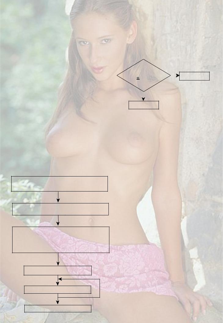
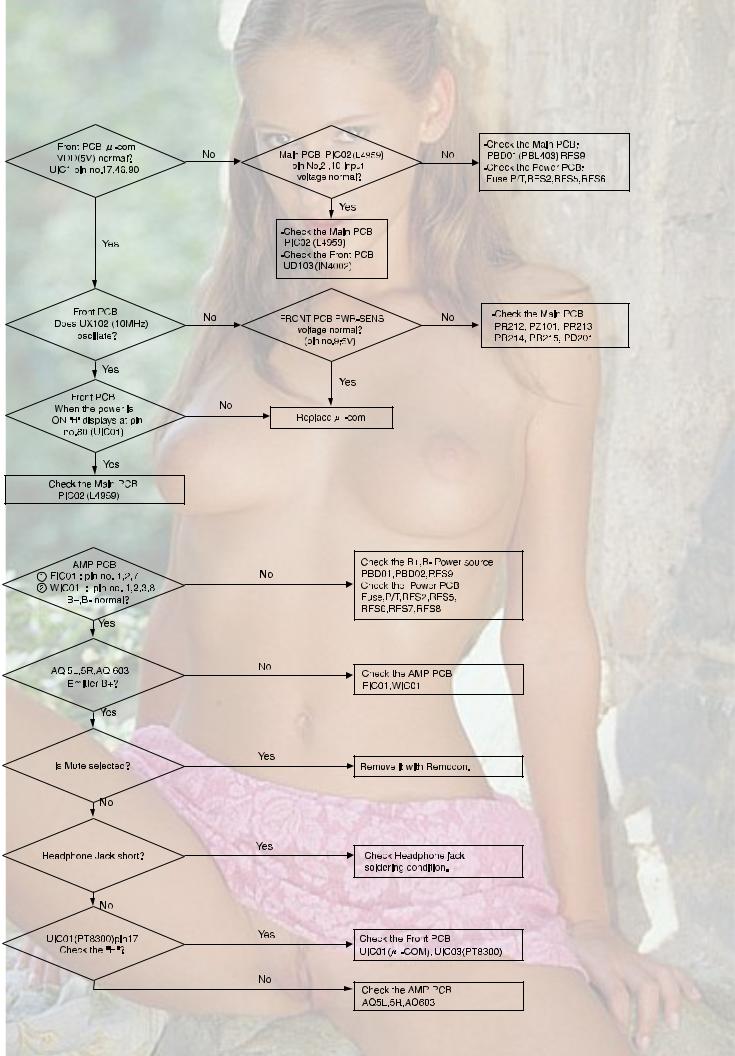
Troubleshooting
1. Amplifier
Power malfunction
No output
1-26
MA-GA77
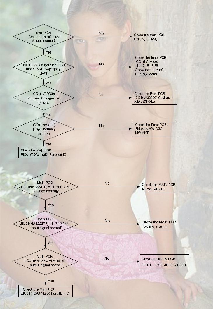
2.Tuner malfunction (FM/AM)
3.Tape
1-27

MX-GA77
4.CD
1-28
MA-GA77
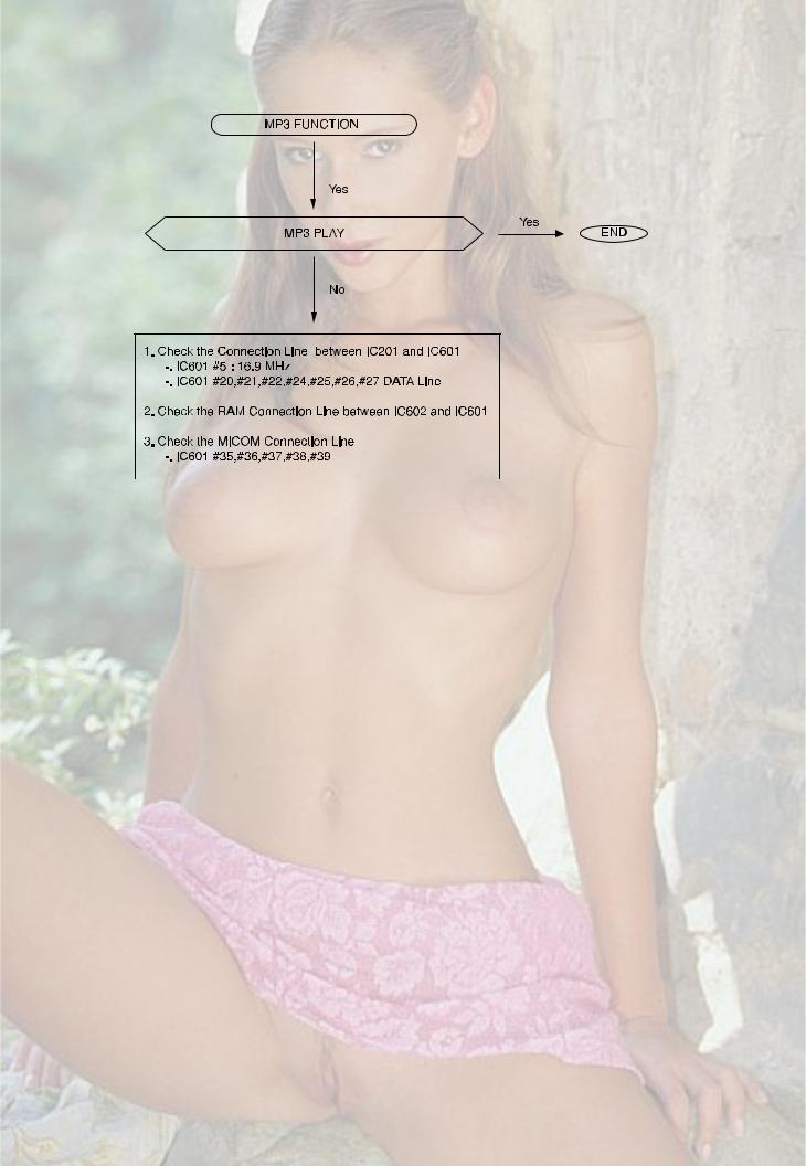
5.CD - MP3 parts
1-29
MX-GA77
Description of major ICs
 LC876764 (UIC1) : Microcontroller
1.Pin layout |
S47/PF7 |
S46/PF6 |
S45/PF5 |
S44/PF4 |
S43/PF3 |
S42/PF2 |
S41/PF1 |
S40/PF0 |
VDD4 |
S39/PE7 |
S38/PE6 |
S37/PE5 |
S36/PE4 |
S35/PE3 |
S34/PE2 |
S33/PE1 |
S32/PE0 |
S31/PD7 |
S30/PD6 |
S29/PD5 |
S28/PD4 |
S27/PD3 |
S26/PD2 |
S25/PD1 |
S24/PD0 |
S23/PC7 |
S22/PC6 |
|
|
|
|
|
|
|
|
|
|
|
|
|
|
|
|
|
|
|
|
|
|
|
|
|
|
|
|
|
80 |
79 |
78 |
77 |
76 |
75 |
74 |
73 |
72 |
71 |
70 |
69 |
68 |
67 |
66 |
65 |
64 |
63 |
62 |
61 |
60 |
59 |
58 |
57 |
56 |
55 |
54 |
S48/PG0 |
81 |
|
|
|
|
|
|
|
|
|
|
|
|
|
|
|
|
|
|
|
|
|
|
|
|
|
|
S49/PG1 |
82 |
|
|
|
|
|
|
|
|
|
|
|
|
|
|
|
|
|
|
|
|
|
|
|
|
|
|
S50/PG2 |
83 |
|
|
|
|
|
|
|
|
|
|
|
|
|
|
|
|
|
|
|
|
|
|
|
|
|
|
S51/PG3 |
84 |
|
|
|
|
|
|
|
|
|
|
|
|
|
|
|
|
|
|
|
|
|
|
|
|
|
|
P00 |
85 |
|
|
|
|
|
|
|
|
|
|
|
|
|
|
|
|
|
|
|
|
|
|
|
|
|
|
P01 |
86 |
|
|
|
|
|
|
|
|
|
|
|
|
|
|
|
|
|
|
|
|
|
|
|
|
|
|
P02 |
87 |
|
|
|
|
|
|
|
|
|
|
|
|
|
|
|
|
|
|
|
|
|
|
|
|
|
|
P03 |
88 |
|
|
|
|
|
|
|
|
|
|
|
|
|
|
|
|
|
|
|
|
|
|
|
|
|
|
VSS2 |
89 |
|
|
|
|
|
|
|
|
|
|
|
|
|
|
|
|
|
|
|
|
|
|
|
|
|
|
VDD2 |
90 |
|
|
|
|
|
|
|
|
|
|
|
|
|
|
|
|
|
|
|
|
|
|
|
|
|
|
P04 |
91 |
|
|
|
|
|
|
|
|
|
|
|
|
|
|
|
|
|
|
|
|
|
|
|
|
|
|
P05 |
92 |
|
|
|
|
|
|
|
|
|
|
|
|
|
|
|
|
|
|
|
|
|
|
|
|
|
|
P06 |
93 |
|
|
|
|
|
|
|
|
|
|
|
|
|
|
|
|
|
|
|
|
|
|
|
|
|
|
P07 |
94 |
|
|
|
|
|
|
|
|
|
|
|
|
|
|
|
|
|
|
|
|
|
|
|
|
|
|
P10/SO0 |
95 |
|
|
|
|
|
|
|
|
|
|
|
|
|
|
|
|
|
|
|
|
|
|
|
|
|
|
P11/SI0/SB0 |
96 |
|
|
|
|
|
|
|
|
|
|
|
|
|
|
|
|
|
|
|
|
|
|
|
|
|
|
P12/SCK0 |
97 |
|
|
|
|
|
|
|
|
|
|
|
|
|
|
|
|
|
|
|
|
|
|
|
|
|
|
P13/SO1 |
98 |
|
|
|
|
|
|
|
|
|
|
|
|
|
|
|
|
|
|
|
|
|
|
|
|
|
|
P14/SI1/SB1 |
99 |
|
|
|
|
|
|
|
|
|
|
|
|
|
|
|
|
|
|
|
|
|
|
|
|
|
|
P15/SCK1 |
100 |
|
|
|
|
|
|
|
|
|
|
|
|
|
|
|
|
|
|
|
|
|
|
|
|
|
|
|
1 2 3 4 5 6 7 8 9 10 11 12 13 14 15 16 17 18 19 20 21 22 23 24 25 26 27 |
||||||||||||||||||||||||||
2.Block diagram |
P16/T1PWML |
P17/T1PWMH/BUZ |
P30/INT4/T1IN |
P31/INT4/T1IN |
P32/INT4/T1IN |
P33/INT4/T1IN |
P34/INT5/T1IN |
P35/INT5/T1IN |
P36/INT5/T1IN |
P37/INT5/T1IN |
RES |
XT1/AN10 |
XT2/AN11 |
VSS1 |
CF1 |
CF2 |
VDD1 |
P80/AN0 |
P81/AN1 |
P82/AN2 |
P83/AN3 |
P84/AN4 |
P85/AN5 |
P86/AN6 |
P87/AN7/MICIN |
P70/INT0/T0LCP/AN8 |
P71/INT1/T0HCP/AN9 |
|
|
|
|
|
|
|
|
|
|
|
|
|
|
|
|
|
|
|
|
|
|
|
|
|
|
|
|
Interrupt Control |
|
|
|
|
|
|
|
|
|
|
|
|
|
|
IR |
|
|
|
PLA |
|
|
|
|
|
|||
|
|
|
|
|
|
|
|
|
|
|
|
|
|
|
|
|
|
|
|
|
|
|
|
||||
Stand-by Control |
|
|
|
|
|
|
|
|
|
|
|
|
|
|
|
|
ROM |
|
|
|
|
|
|
|
|||
CF |
Clock Generator |
|
|
|
|
|
|
|
|
|
|
|
|
|
|
|
|
|
|
|
|
|
|
|
|
|
|
RC |
|
|
|
|
|
|
|
|
|
|
|
|
|
|
|
|
|
|
|
|
|
|
|
|
|
|
|
|
|
|
|
|
|
|
|
|
|
|
|
|
|
|
|
|
|
|
|
|
|
|
|
|
|
|
|
MRC |
|
|
|
|
|
|
|
|
|
|
|
|
|
|
|
|
|
|
PC |
|
|
|
|
|
|
|
|
X’ tal |
|
|
|
|
|
|
|
|
|
|
|
|
|
|
|
|
|
|
|
|
|
|
|
|
|
|
|
|
Bus Interface |
|
|
|
|
|
|
|
|
|
|
|
ACC |
|
|
|
|
|
|
|
|||||||
|
|
|
|
|
|
|
|
|
|
|
|
|
|
|
|
|
|
|
|
|
|
||||||
SIO0 |
|
|
Port 0 |
|
|
|
|
|
|
|
|
|
|
|
B Register |
|
|
|
|
|
|
||||||
SIO1 |
|
|
Port 1 |
|
|
|
|
|
|
|
|
|
|
|
C Register |
|
|
|
|
|
|
||||||
Timer 0 |
|
|
Port 3 |
|
|
|
|
|
|
|
|
|
|
|
|
|
|
|
|
|
|
|
|
|
|
||
(High speed clock counter) |
|
|
|
|
|
|
|
|
|
|
|
|
|
|
|
|
|
|
|
|
|
|
|
|
|||
|
|
|
|
|
|
|
|
|
|
|
|
|
|
|
|
|
|
|
|
|
|
|
|
|
|
|
|
|
|
|
|
|
|
|
|
|
|
|
|
|
|
|
|
|
|
|
|
AL U |
|
|
|
|
|
|
|
Timer 1 |
|
|
Port 7 |
|
|
|
|
|
|
|
|
|
|
|
|
|
|
|
|
|
|
|
|
|
|
||
|
|
|
|
|
|
|
|
|
|
|
|
|
|
|
|
|
|
|
|
|
|
|
|
|
|
|
|
Base Timer |
|
|
Port 8 |
|
|
|
|
|
|
|
|
|
|
|
|
PSW |
|
|
|
|
|
|
|
||||
VFD Controller |
|
|
ADC |
|
|
|
|
|
|
|
|
|
|
|
|
|
RAR |
|
|
|
|
|
|
|
|||
INT 0 - 5 |
Weak Signal |
|
|
|
|
|
|
|
|
|
|
|
RAM |
|
|
|
|
|
|
|
|||||||
Noise Rejection |
|
Detector |
|
|
|
|
|
|
|
|
|
|
|
|
|
|
|
|
|
|
|
||||||
|
|
|
|
|
|
|
|
|
|
|
|
|
|
|
|
|
|
|
|
|
|
|
|||||
Timer 4 |
|
Timer 6 |
|
|
|
|
|
|
|
|
|
|
Stack Pointer |
|
|
|
|
|
|
||||||||
|
|
|
|
|
|
|
|
|
|
|
|
|
|
|
|
|
|
|
|
|
|
||||||
Timer 5 |
|
Timer 7 |
|
|
|
|
|
|
|
|
|
|
Watch Dog Timer |
|
|
|
|
||||||||||
1-30 |
|
|
|
|
|
|
|
|
|
|
|
|
|
|
|
|
|
|
|
|
|
|
|
|
|
|
|
S21/PC5 |
S20/PC4 |
|
|
|
|
|
|
|
53 |
52 |
|
28 |
29 |
|
|
|
|
P72/INT2/T0IN/NKIN/AN12 |
P73/INT3/T0IN/AN13 |
|
FIX0
51
50
49
48
47
46
45
44
43
42
41
40
39
38
37
36
35
34
33
32
31 30
S0/T0
S19/PC3
S18/PC2
S17/PC1
S16/PC0
VDD3
S15/T15
S14/T14
S13/T13
S12/T12
S11/T11
S10/T10
S9/T9
 S8/T8
S8/T8
 S7/T7
S7/T7
 S6/T6
S6/T6
 S5/T5
S5/T5
 S4/T4
S4/T4
 S3/T3
S3/T3
 S2/T2
S2/T2
 S1/T1
S1/T1
 Loading...