

Page 1
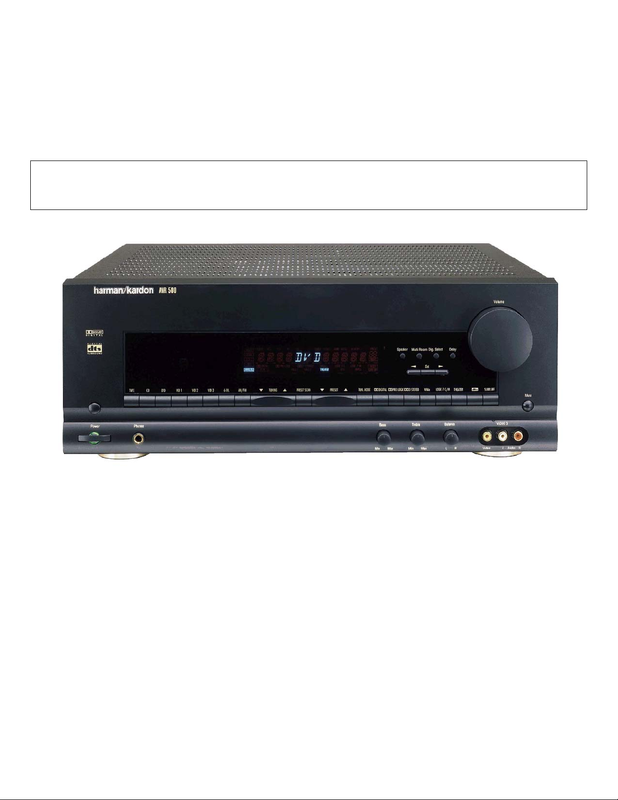
harman/kardon
AVR500
A/V DOLBY DIGITAL RECEIVER
SERVICE MANUAL
CONTENTS
SPECIFICATIONS ………………………………..…2
ESD WARNINGS…………………………………… 4
LEAKAGE TEST……………………………………. 5
CONTROLS AND FUNCTIONS……………………6
SERVICE PROCEDURE………………………….. .9
TEST EQUIPMENT REQUIRED……………… …9
ALIGNMENT PROCEDURES………………………9
ALIGNMENT AND TEST POINTS……………….. 11
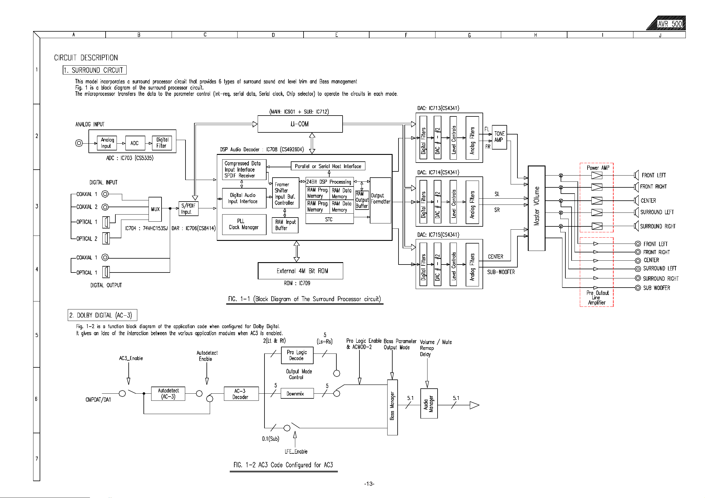
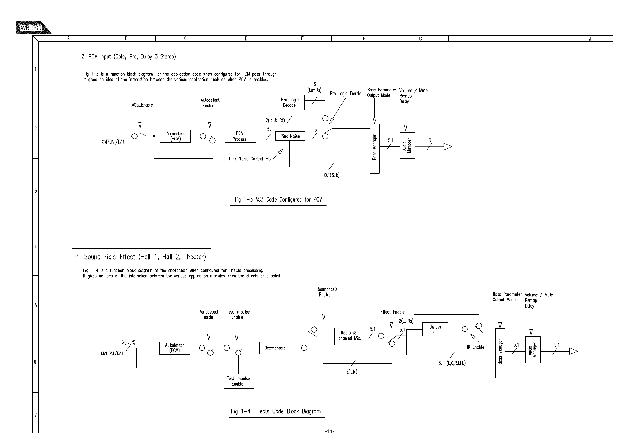
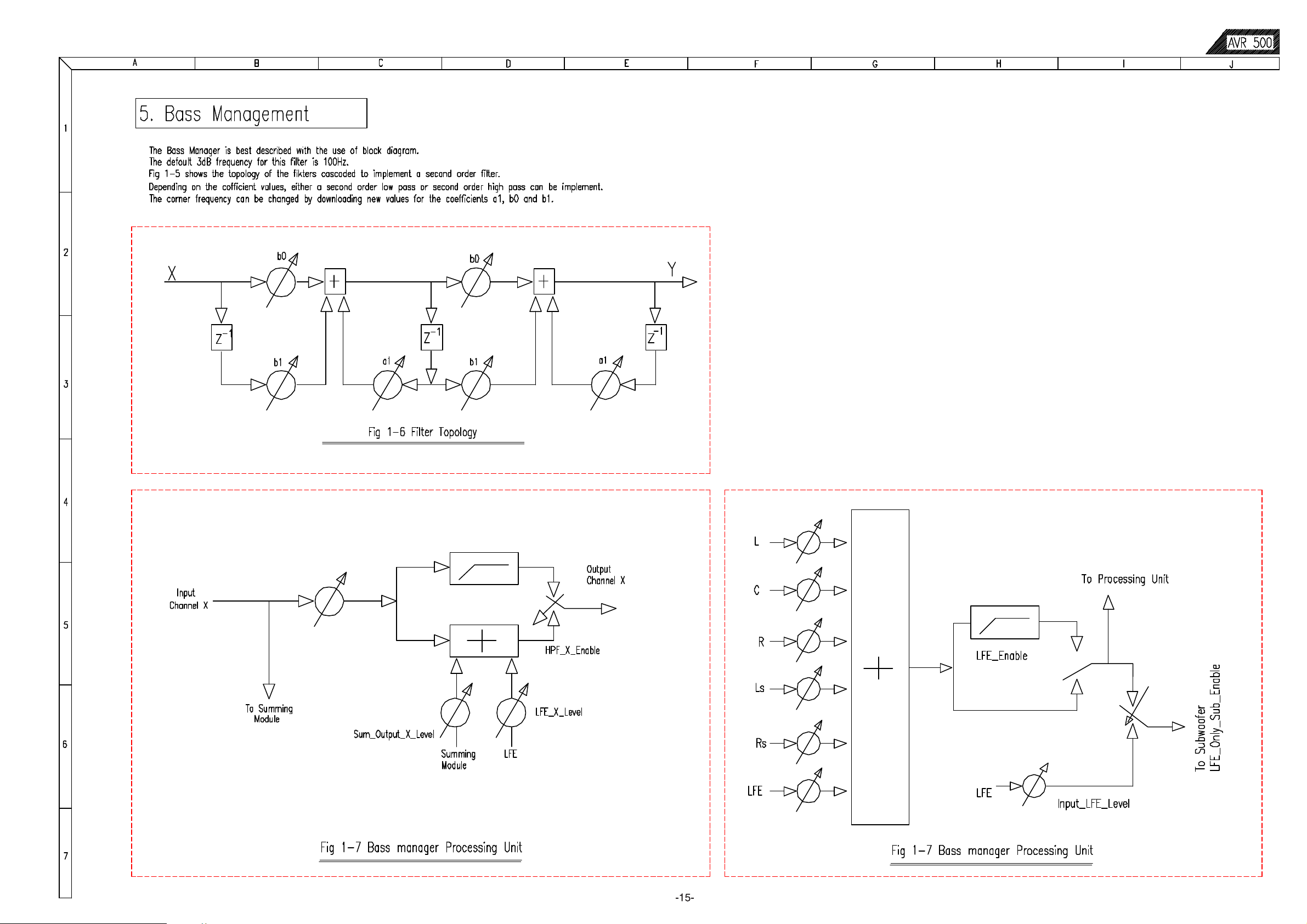
CIRCUIT DESCRIPTION…………………………..13
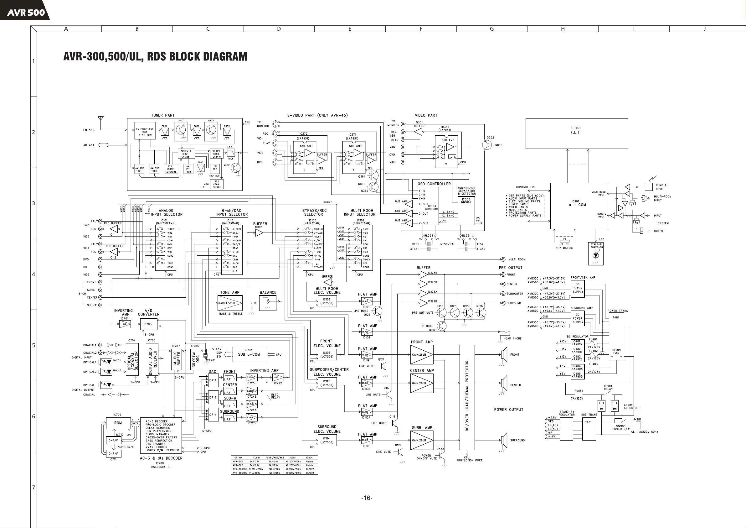
BLOCK DIAGRAM ………………………………….16
BULLETIN HK2000-02……………..………..……..17
BULLETIN HK2000-04………………...….………..19
BULLETIN HK2000-05………………...….………..21
harman/kardon, Inc.
250 Crossways Park Dr.
Woodbury, New York 11797 Rev1 – 11/2003
DISASSEMBLY PROCEDURES ………… .……23
GENERAL UNIT PARTS LIST …………………..24
GENERAL UNIT EXPLODED VIEW………..….. 26
PC . BOARDS …………………………………..…27
ELECTRICAL PARTS LIST ………………….…..32
IC BLOCK DIAGRAMS …………………….….….55
CPU PIN CONFIGURATION……………….…….75
FLT PIN CONFIGURATION………………….…. 76
SCHEMATIC DIAGRAMS ……………..…….…..83
PIN CONNECTION DIAGRAM …………….……92
WIRING DIAGRAM ………………………….……93
PACKING MATERIAL AND PARTS LIST………94
Page 2
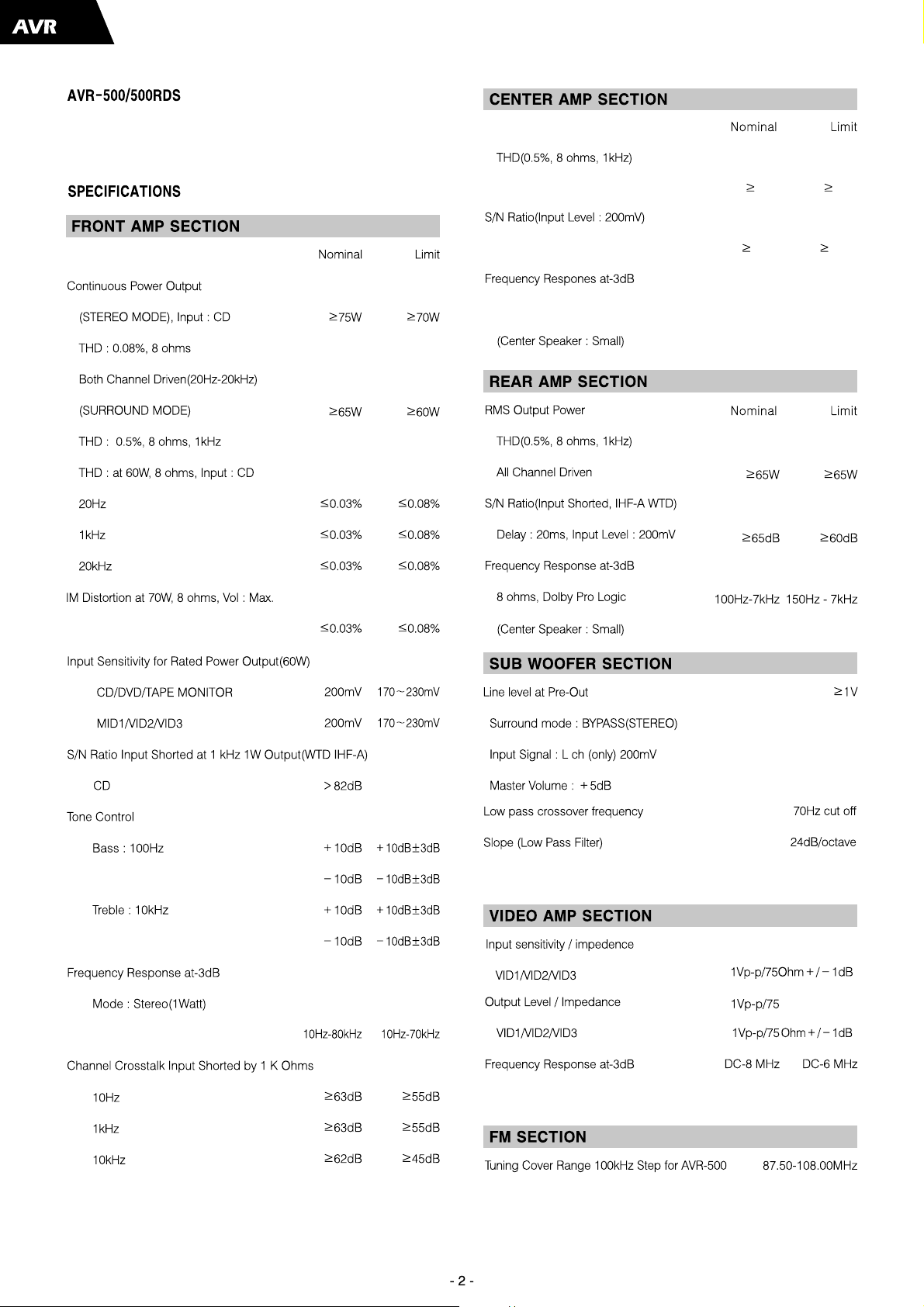
500
RMS Output Power
All Channel Driven
Input Shorted, IHF-A WTD
8 ohms, Dolby Pro Logic
65W 65W
65dB 60dB
100Hz-20kHz 150Hz-20kHz
Page 3
500
Page 4
500
Some semiconductor (solid state) devices can be damaged easily by static electricity. Such components commonly are called
Electrostatically Sensitive (ES) Devices. Examples of typical ES devices are integrated circuits and some field effect transistors and
semiconductor "chip" components.
The following techniques should be used to help reduce the incidence of component damage caused by static electricity.
1. Immediately before handling any semiconductor component or semiconductor-equipped assembly, drain off any electrostatic charge on
your body by touching a known earth ground. Alternatively, obtain and wear a commercially available discharging wrist strap device,
which should be removed for potential shock reasons prior to applying power to the unit under test.
2. After removing an electrical assembly equipped with ES devices, place the assembly on a conductive surface such as aluminum foil, to
prevent electrostatic charge build-up or exposure of the assembly.
3. Use only a grounded-tip soldering iron to solder or unsolder ES devices.
4. Use only an anti-static solder removal device. Some solder removal devices not classified as "anti-static" can generate electrical charges
sufficient to damage ES devices.
5. Do not use freon-propelled chemicals. These can generate electrical change sufficient to damage ES devices.
6. Do not remove a replacement ES device from its protective package until immediately before you are ready to install it. (Most replacement
ES devices are packaged with leads electrically shorted together by conductive foam, aluminum foil or comparable conductive material.)
7. Immediately before removing the protective material from the leads of a replacement ES device, touch the protective material to the
chassis or circuit assembly into which the device will be installed.
CAUTION :
8. Minimize bodily motions when handling unpackaged replacement ES devices. (Otherwise harmless motion such as the brushing together
or your clothes fabric or the lifting of your foot from a carpeted floor can generate static electricity sufficient to damage an ES devices.
Be sure no power is applied to the chassis or circuit, and observe all other safety precautions.
Each precaution in this manual should be followed during servicing.
Components identified with the IEC symbol in the parts list are special significance to safety. When replacing a component identified with
, use only the replacement parts designated, or parts with the same ratings or resistance, wattage, or voltage that are designated in the
parts list in this manual. Leakage-current or resistance measurements must be made to determine that exposed parts are acceptably
insulated from the supply circuit before retuming the product to the customer.
-4-
Page 5
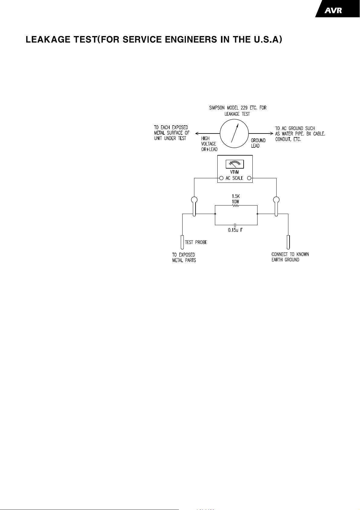
Before returning the unit to the user, perform the following safety checks :
1. lnspect all lead dress to make certain that
leads are not pinched or that hardware is not
lodged between the chassis and other metal
parts in the unit.
2. Be sure that any protective devices such as
nonmetallic control knobs, insulating fish-
papers, cabinet backs, adjustment and
500
compartment covers or shields, isolation
resistor-capacity networks, mechanical
insulators, etc. Which were removed for the
servicing are properly re-installed.
3. Be sure that no shock hazard exists ; check for leakage
current using Simpson Model 229 Leakage Tester, standard
equipment item No. 21641, RCA Model WT540A or use
alternate method as follows : Plug the power cord directly
Into a 120 volt AC receptacle (do not use an Isolation
Transformer for this test). Using two clip leads, connect a
1500 ohms, 10watt Resistor paralleled by a 0.15uF capacitor, in series with all exposed metal cabinet parts and a known earth ground, such
as a water pipe or conduit. Use a VTVM or VOM with 1000 ohms per volt, or higher sensitivity to measure the AC voltage drop across the
resistor. (See diagram) Move the resistor connection to each exposed metal part having a return path to the chassis (antenna, metal, be
performed with the 0.35 volt RMS or more is excessive and indicates a potential shock hazard which must be corrected before returning the
unit to the owner.
-5-
Page 6
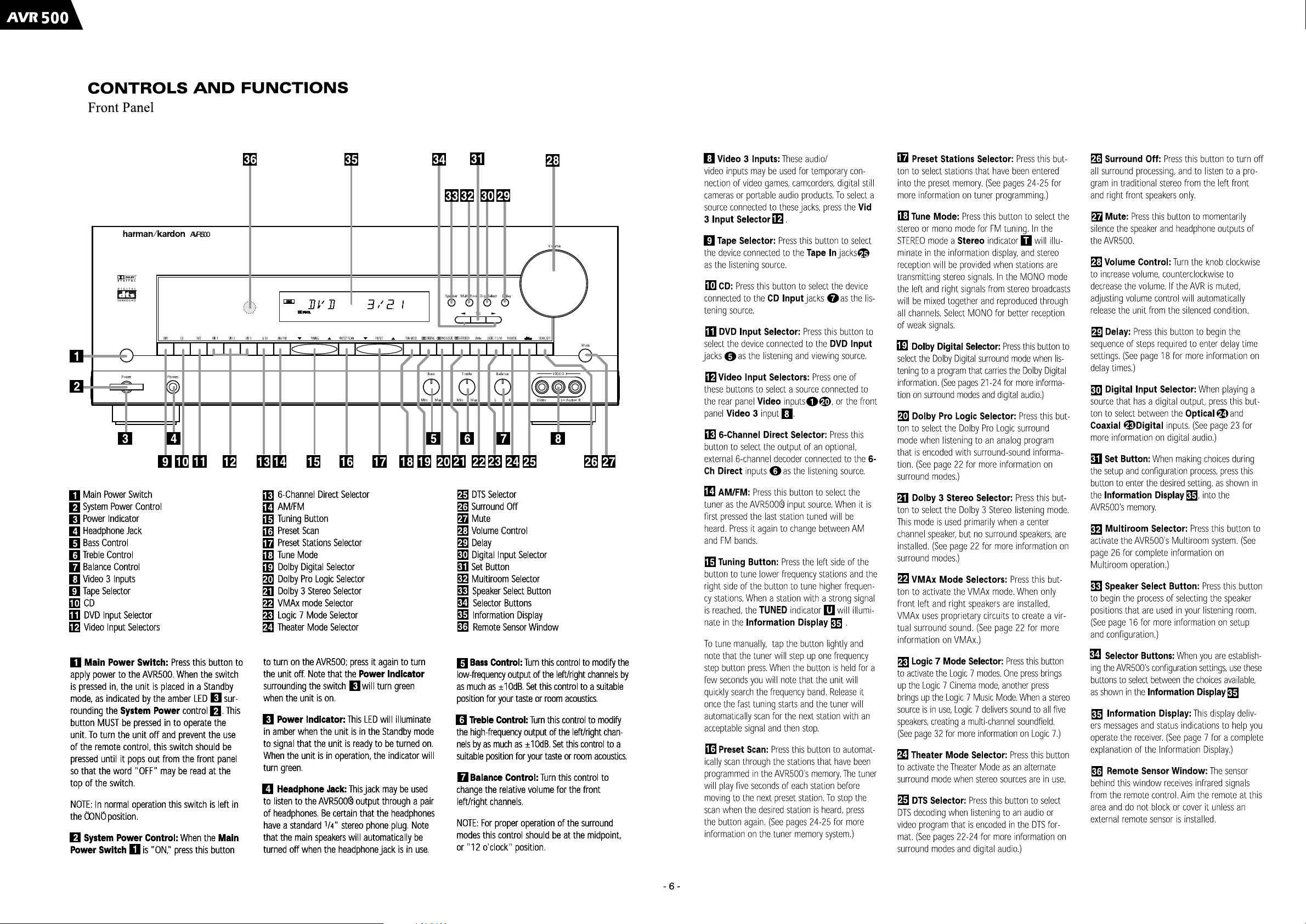
Page 7
LR
SLEEP TUNED
STEREO
AUTOMONO PRESET
SURR. OFF
MUTE
PCM THEATER
LOGIC 7 C LOGIC 7 MVMAx3
-
STEREOPRO LOGICDIGITAL
COAX
OPT
12
ANALOG
NIGHT
MULTI
MEMORY
A
B
C
D
EG
N
O
K
M
L
X
WTUSRQ PV
F
H
I
J
A Coax Source
B Digital Source Input Number
C Optical Source
D Analog Source Indicator
E PCM Indicator
F Dolby Digital Indicator
G Analog Dolby Surround Mode Indicators
H VMAx Mode Indicator
I Theater Mode Indicator
J Logic 7 Mode Indicators
K DTS Mode Indicator
L Surround Off
M Multiroom System Indicator
N Night Mode Indicator
O Preset Number
P Preset Indicator
Q Memory
R Auto
S Mono Indicator
T Stereo Indicator
U Tuned Indicator
V Main Information Display
W Sleep Indicator
X Mute
A Coax Source:This indicator illuminates
when a digital source is in use via a connection
to the Coaxial Digital inputs e.
B Digital Source Input Number:These
indicators tell you which of the two digital
inputs is selected.This indicator works in cojunction with the Coax Source A and Optical
Source C indicators to show which form of
digital signal is in use.
C Optical Source:This indicator illuminates
when a digital source is in use via a connection
to the Optical Digital input d.
D Analog Source Indictor: This indicator
illuminates when an analog input source is in use.
E PCM Indicator:This indicator illuminates
to show that a standard PCM (S/P-DIF) digital
audio signal is being decoded by the digital-toanalog converter.
F Dolby Digital Indicator:This indicator
illuminates when a Dolby Digital source is
being played.
G Analog Dolby Surround Mode
Indicators:These indicators illuminate when
one of the analog (matrix) Dolby Surround
modes is in use.
H VMAx Mode Indicator: This indicator illu-
minates to show that the VMAx mode is in use.
I Theater Mode Indicator: This indicator illu-
minates to show that the Theater mode is in use.
J Logic 7 Mode Indicators:These indica-
tors illuminate when the Logic 7 mode is in
use.LOGIC 7C appears for the Cinema ver-
sion of Logic 7, LOGIC 7M appears for the
Music version of Logic 7.
K DTS Mode Indicator:This indicator illumi-
nates when a DTS-encoded source is playing.
L Surround Off:This indicator illuminates
when the surround processing has been disabled by pressing the Surround Off button
Ù.When this indicator is lit, the AVR 500 will
play traditional stereo sound using the front-left
and front-right speakers only.
M Multiroom System Indicator:This indica-
tor illuminates when the multiroom system is in
operation.(See page 26 for more information
on the multiroom system.)
N Night Mode Indicator:This indicator
lights when the AVR 500 is in the Night mode,
which preserves the dynamic range of digital
program material at low volume levels.
O Preset Number:This two-digit display
indicates the station preset number that is
currently in use,or that is being entered.
P Preset Indicator:This indicator illuminates
when a station previously entered into the preset
memory is tuned.The number that appears below
the indicator is the preset station’s memory.
Q Memory:This indicator flashes when
entering presetsand other information into the
tuner’smemory.
R Auto: This indicator illuminates when the
Auto mode is in use for FM tuning.
S Mono Indicator:This indicator illuminates
when the tuner has been placed in the monaural
mode by pressing the Tune Mode button *.
Set the tuner for mono listening to reduce noise
and improve the quality of distant stereo signals.
T Stereo Indicator:This indicator illuminates
when an FM station is being tuned in stereo.
U Tuned Indicator:This indicator illuminates
when a station is being received with sufficient signal strength to provide acceptable listening quality.
V Main Information Display:This display
shows messages relating to the status,input
source,surround mode,tuner,volume level or
other aspects of unit’s operation.
W Sleep Indicator:This indicator is illumi-
nated when the Sleep function is in use.The
number that appears above the indicator is
the number of minutes remaining before the
AVR 500 will return to the Standby mode.
X Mute:This indicator illuminates to remind
you that the AVR 500’s output has been
silenced by pressing the Mute button ıf.
Press the Mute button again to return to the
previously selected output level.
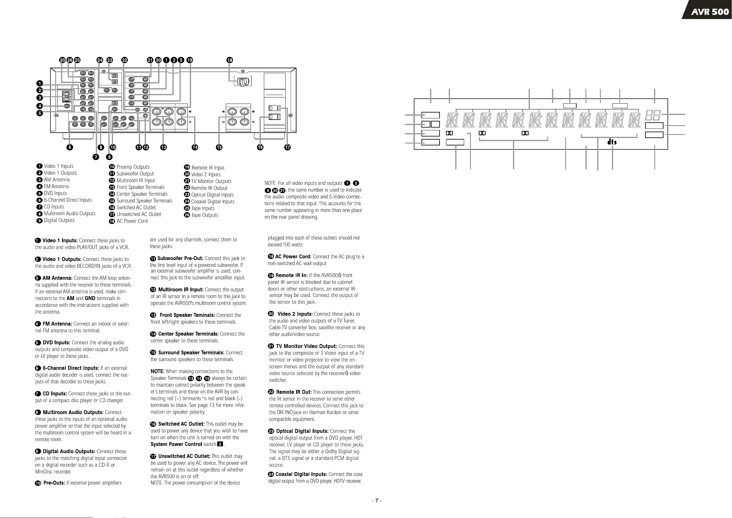
IN
TAPE
OUT
VIDEO
2
ANTENNA
IN
VIDEO
AM
1
OUT
GND
DVD
FM
(75½)
CD
SL
SR FRSUB WOOFER
6 CH. DIRECT MULTI OUT PRE OUT
FLCENTER
DIGITAL INPUT
OPTICAL
2
OPTICAL
1
COAXIAL 2 COAXIAL 1
DIGITAL INPUT
DIGITAL OUTPUT
OPTICAL
1
COAXIAL
1
ML
MR
VIDEO
TV
MONITOR
OUT
VIDEO 2
IN
VIDEO 1
VIDEO 1
OUT
DVD
OUT IN
REMOTE
CONTROL
SL
SUB WOOFERFL
MULTI IN
SR CENTERFR
RIGHT
SPEAKERS 8 Ohms SPEAKER 8 Ohm
FRONT
CENTER
LEFT CENTER
AC ~ 120V 60 Hz
SURROUND
RIGHT
SPEAKERS 8 Ohms
LEFT
MODEL NO. AVR 500
HARMAN KARDON
NORTHRIDGE
CALIFORNIA, USA
AC OUTLETS
(120V.60Hz)
TOTAL 150W or 1.5A MAX
UNSWITCHED
TOTAL 100W or 1A MAX.
SWITCHED
TOTAL 150W or 0.5A MAX.
SERIAL NO.
Page 8
Page 9
500
SERVICE PROCEDURE
1. All Clear
This service program can clear all memorized operations and functions.
When the POWER ON, press the "AM/FM" button while pressing the "PRO LOGIC"button.
After this, Preset memory will be set to these frequencies.
FM
AM
VERSION
120
230RDS
VERSION
120
230RDS
P1
87.5
87.50
P9
520
522
P2
88.0
88.00
P10
600
594
P3
90.0
90.00
P11
610
999
2. VFD segment illumination & text
This set do not have VFD segment check function because lack of u-com memory size
So For your checking VFD states according to each function
Please refer to owners manual process.
TEST EQUIPMENT REQUIRED
1) AM/FM Signal generator
2) Digital Multimeter
3) Distortion lever meter
P4
95.0
95.00
P12
1000
1395
P5
98.0
98.00
P13
1400
1611
P6
99.0
99.00
P14
1500
P7
106.0
106.00
P15
1710
P8
108.0
108.00
4. FM STEREO Separation Adjustment
Input Signal Source
step
1
2
Connection
Signal generator
output to FM
antenna
terminal.(750hm)
Signal
Frequency
98MHz
4. AM OSC Adujstment
Input Signal Source
step
1
Connection
Signal Generator
output to transmission
loop antenna
(standard required loop)
Signal
Frequency
522kHz
(230,230RDS)
520kHz(120)
Source Signal Output Level and
Modulation
same specification as
distortion adjustment.
Input only L channel
same specification as
distortion adjustment.
Input only R channel
Source Signal Output Level and
Modulation
5mV/m(74dBu)
MOD.30%
FM STEREO
FM STEREO
400Hz
Reception
Frequency
98MHz
(P5)
98MHz
(P5)
Reception
Frequency
522kHz
(230,230RDS)
520kHz
(120)
(P9)
Adjustment
Point
VR803
VR803
Adjustment
Point
T802
Adjustment
Value
Output level
at TAPE-OUT
channel R
Output level
at TAPE-OUT
channel R
Adjustment
Value
1.1V 1.2V
Minimum
Minimum
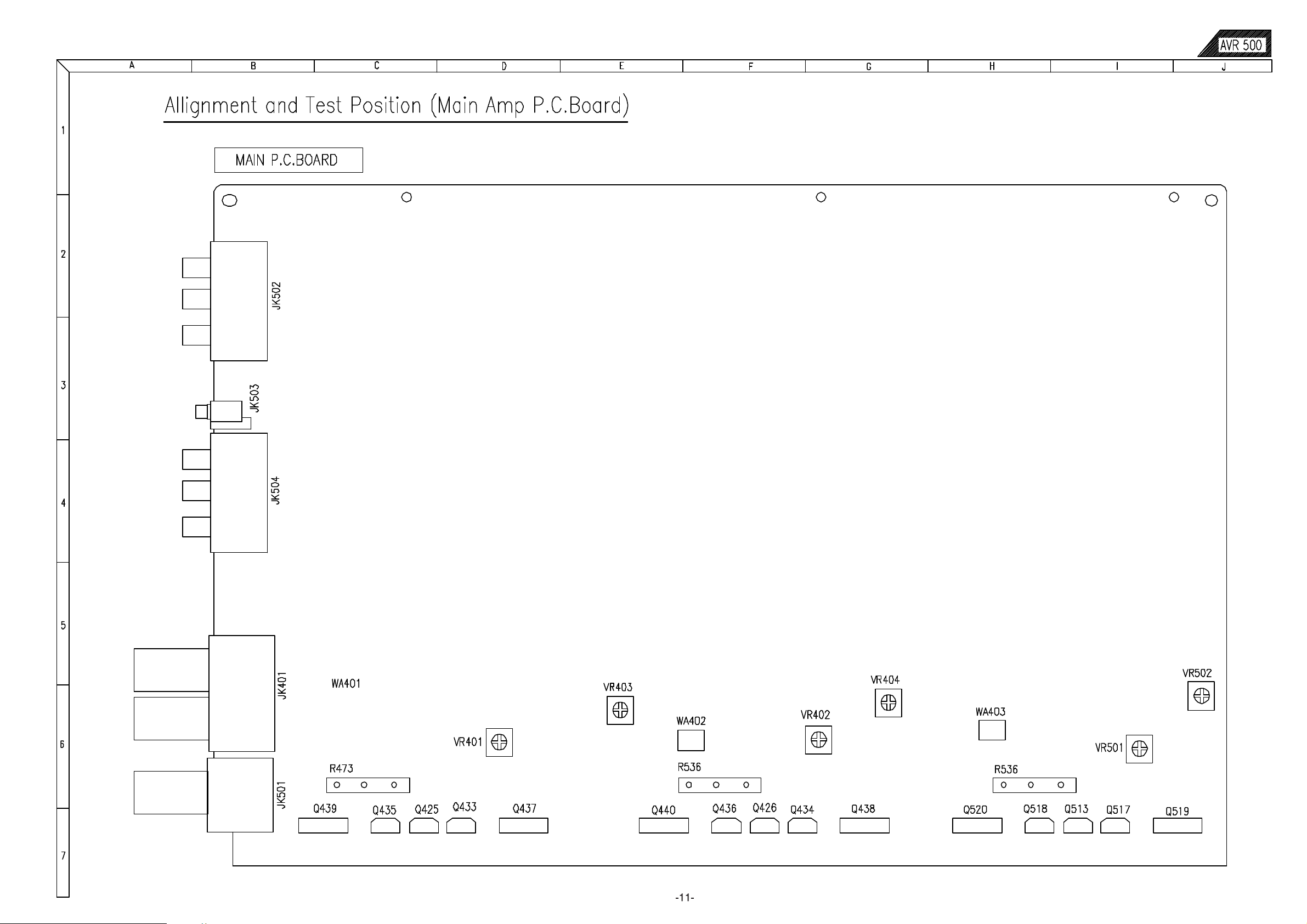
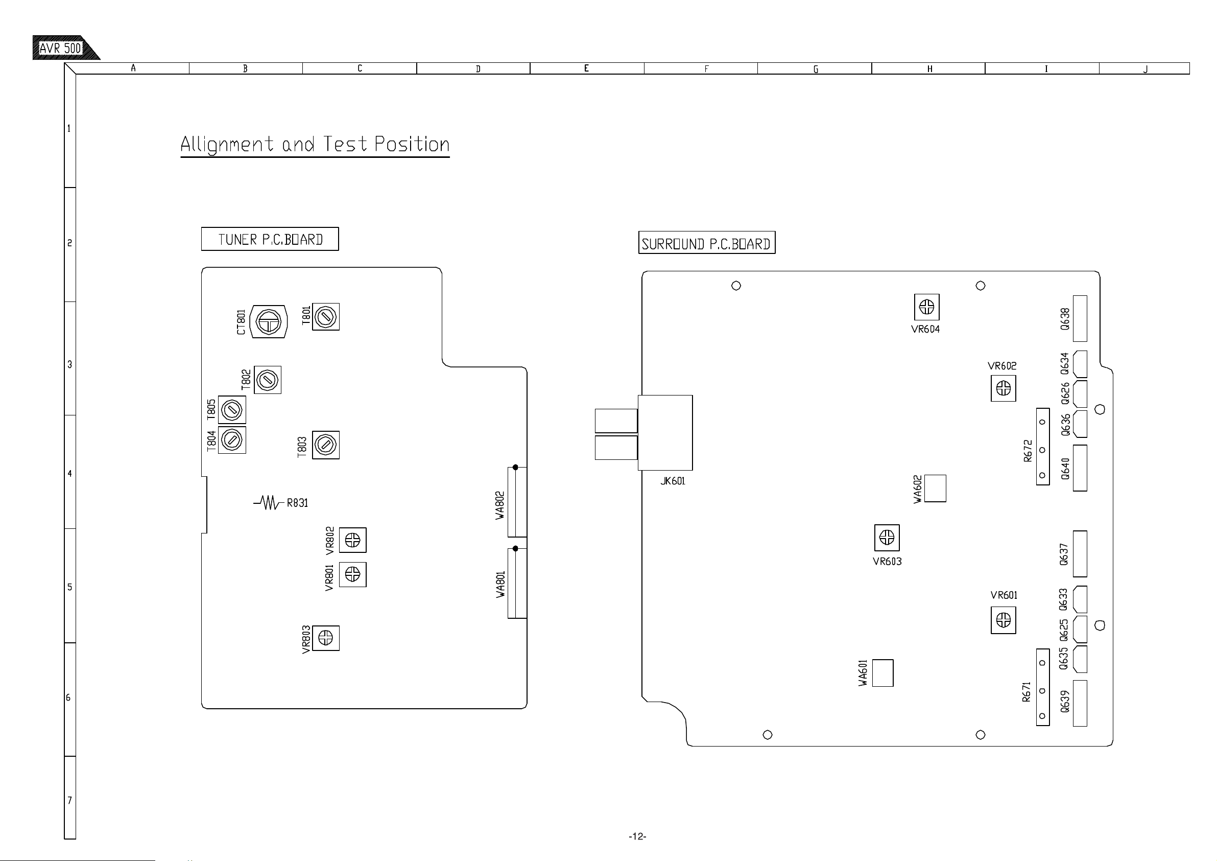
ALIGNMENT PROCEDURES
1. FM MONO. Distortion adjustment
Input Signal Source
step
1
2
Connection
Signal generator
output to FM
antenna
terminal.(750hm)
Signal
Frequency
98MHz
Source Signal Output Level and
Modulation
1000uV/m (60dBu)
MONO 1kHz/
Dev. 75kHz
2. FM MUTING LEVEL ADJUSTMENT
Turn variable resistor VR801 and stop at position "TUNED" is not shown (not indicated), then again turn the variable resistor VR801 to the
opposite revolution and stop at a position "TUNED" is shown.
Input Signal Source
step
1
2
Connection
Signal generator
output to FM
antenna
terminal.(750hm)
Signal
Frequency
98MHz
Source Signal Output Level and
Modulation
10uV/m (20dBu)
MONO 1kHz/
Dev. 75kHz
Reception
Frequency
98MHz
(P5)
Reception
Frequency
98MHz
(P5)
AUTO
SCAN
Adjustment
Point
T804
T805
Adjustment
Point
VR801
Only confirm
Adjustment
Value
0mV 0.5mV
(R831)
Distortion
level
Minimum
TAPE-OUT
Adjustment
indicate on VFD
indicate on VFD
at
Value
"TUNED"
"TUNED"
5. AM-Tracking Adjustment (MW)
Input Signal Source
step
1
2
Connection
Signal Generator
output to transmission
loop antenna
(standard required loop)
Frequency
(230,230RDS)
600kHz(120)
(230,230RDS)
1400kHz(120)
6. AM IF Adjustment
Input Signal Source
step
1
Connection
Signal Generator
output to transmission
loop antenna
(standard required loop)
Frequency
(230,230RDS)
1000kHz(120)
Signal
594kHz
1395kHz
Signal
999kHz
Source Signal Output Level and
Modulation
5mV/m(74dBu)
400Hz
MOD.30%
Source Signal Output Level and
Modulation
5mV/m(74dBu)
400Hz
MOD.30%
Reception
Frequency
594kHz
(230,230RDS)
600kHz(120)
Reception
Frequency
999kHz
(230,230RDS)
1000kHz
(120)
Adjustment
Point
T801
CT801
Adjustment
Point
T803
Adjustment
Value
Output level(L or R)
Minimum
TAPE-OUT
Output level(L or R)
Minimum
TAPE-OUT
Adjustment
Output level(L or R)
Maximum
TAPE-OUT
Output level(L or R)
Maximum
TAPE-OUT
at
at
Value
at
at
-9-
Page 10
500
7. AM auto stop Adjustment
9. Main Amp DC OFFSET VOLTAGE Adjustment
Input Signal Source
step
1
2
Connection
Signal Generator
output to transmission
loop antenna
(standard required loop)
Signal
Frequency
999kHz
(230,230RDS)
1000kHz
(120)
8. Main Amp ldling current Adjustment
(1) SET CONDITION
1) SEMI VOLUME POSITION at MAIN/SURROUND AMP Board; CENTER
MAIN : VR401, VR402, VR501
SURROUND : VR601, VR602
2) NO signal / NO LOAD
3) AC LINE VOLTAGE : 120V/60Hz, 230V/50Hz
Source Signal Output Level and
Modulation
1000uV/m(60dBu)
400Hz
MOD.30%
Reception
Frequency
999kHz
(230,230RDS)
1000kHz(120)
AUTO SCAN
Adjustment
Point
VR802
Only
Confirm
Adjustment
Value
"TUNED"
indicate on
VFD
"TUNED"
indicate on
VFD
(1) SET CONDITION
1) SEMI VOLUME POSITION at MAIN/SURROUND AMP Board; CENTER
MAIN : VR403, VR404, VR502
SURROUND : VR603, VR604
2) NO signal / NO LOAD
3) AC LINE VOLTAGE : 120V/60Hz, 230V/50Hz
(2) After turning on the unit, keep it over than 5MIN. (Keep the Power/Drive TR as normal temperature)
(3) Adjust the voltage value of primary & secondary of wafer to be 10mV by rotating the semi-volume
of each channel to the right
CHANNEL ADJUSTMENT MEASUREMENT OTHERS
FRONT-L ch
FRONT-R ch
CENTER ch
SURROUND-L ch
SURROUND-R ch
VR403
VR404
VR502
VR603
Vr604
JK401
JK402
JK501
JK601
JK601
VOLAGE
0mV
0mV
0mV
0mV
0mV
(2) After turning on the unit, keep it over than 5MIN. (Keep the Power/Drive TR as normal temperature)
(3) Adjust the voltage value of primary & secondary of wafer to be 10mV by rotating the semi-volume
of each channel to the right
CHANNEL ADJUSTMENT MEASUREMENT OTHERS
FRONT-L ch
FRONT-R ch
CENTER ch
SURROUND-L ch
SURROUND-R ch
(4) CAUTION
1) In case that POWER TR or DREVE TR is needed to be replaced for repairing, the corresponding channel
should be adjusted again
* FRONT AMP : Q433~Q440
* CENTER AMP : Q517~Q520
* SURROUND AMP : Q633~Q640
VR401
VR402
VR501
VR601
VR602
WA401
WA402
WA501
WA601
WA602
VOLAGE
10 3mV
10 3mV
10 3mV
10 3mV
10 3mV
R401:22.7mA
R472:22.7mA
R501:22.7mA
R601:22.7mA
R602:22.7mA
(4) CAUTION
1) In case that POWER TR or DREVE TR is needed to be replaced for repairing, the corresponding channel
should be adjusted again
* FRONT AMP : Q401~Q440, Q411~Q414
* CENTER AMP : Q501, Q502, Q506, Q507
* SURROUND AMP : Q601~Q604, Q611~Q614
10. Cautions for main Amp adjustment
(1) At MAIN/SURROUND BOARD, use the below condensors after discharging for sufficent time
for preventing possible damage from electrical spark.
MAIN BOARD C481, C482 (10000/63V, 8200uF/63V)
SURROUND BOARD C691, C692 (6800/63V, 6800uF/50V)
(2) The checker for MAIN/SURROUND BOARD should have the discharging circuit.
Discharge over 30sec. through (407ohm 10w) resistor after turning off
-10-
Page 11
Page 12
Page 13
Page 14
Page 15
Page 16
Page 17
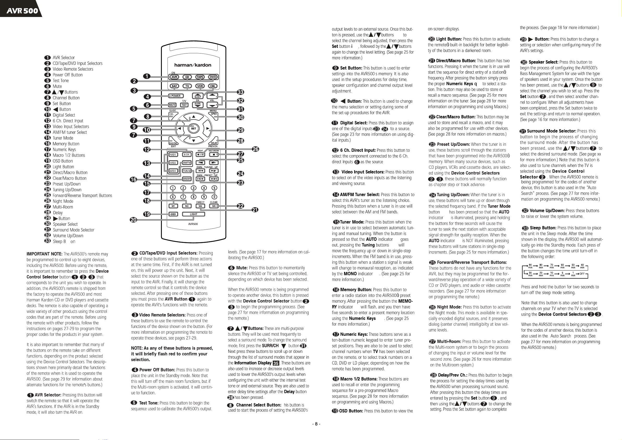
harman/kardon Service Bulletin
Service bulletin # H/K2000-02 Rev1 January 2001 Warranty labor rate: MAJOR repair
To: All harman/kardon Service Centers
Models: AVR300, AVR500
Subject: Random Noise, Erratic Output in DTS Mode
In the event you receive an AVR300 or AVR500 receiver with the complaint “there is distortion, random
noise or gaps in the program material when in the DTS mode”, perform the following procedure:
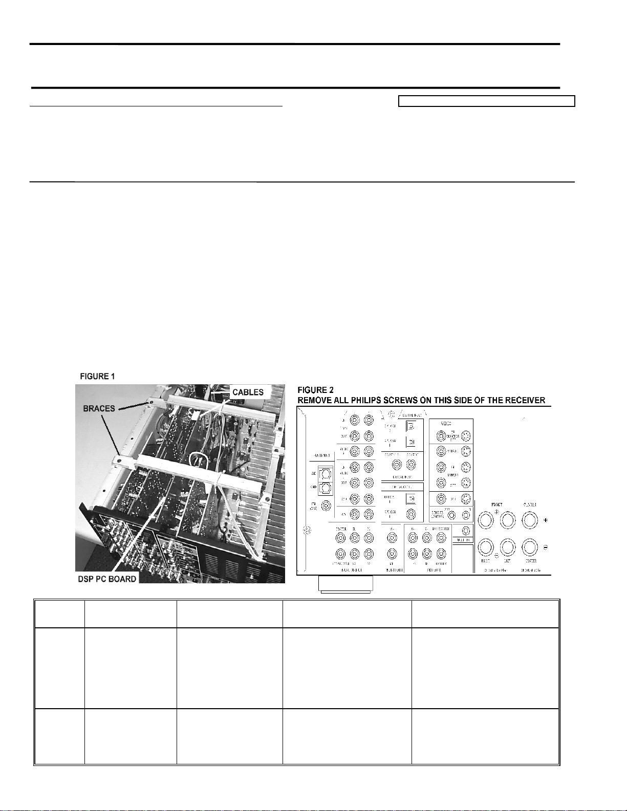
REMOVAL AND MODIFICATION OF THE DSP BOARD
1) Remove the top cover, (14) Black Phillips screws.
2) Locate the DSP PC Board; Figure 1. Remove the two metal braces at the top of the unit. If necessary, cut
the cable ties attached to the braces to move any wires away from the area.
3) Pull the white 22 conductor ribbon cable at the rear of the DSP PC Board straight out of its receptacle.
4) Unplug the white 5 conductor molex cable at the top of the DSP PC Board.
5) Remove the (33) plated Phillips screws on the left side of the rear backplate; see Figure 2. Do not remove
any additional screws on the right side. If using a power tool, use care and minimum effort to avoid damaging
the various plastic receptacles.
6) Remove all three black plastic plugs that cover the optical inputs at the rear of the DSP PC Board.
7) Pull on the left side of the rear backplate, away from the receiver chassis; you should be able to pull it away
enough to allow the DSP PC Board to be pulled straight up and out of the receiver.
8) Proceed with the modifications on page 2.
1
Model Serial Number
120V
AVR300
AVR500
AVR300
AVR500
TH0001-01000
To
TH0001-13886
TH0002-01000
To
TH0002-10460
TH0001-13887
Or higher
TH0002-10461
Or higher
Serial Number
230V RDS
TH0005-01000
To
TH0005-03317
TH0006-01000
To
TH0006-02795
TH0005-03318
Or higher
TH0006-02796
Or higher
STATUS ACTION
Random Noise, Erratic
Output or Gaps in Program
Material when in DTS Mode
Modified by factory NONE REQUIRED
Modifications to DSP Board:
Add ground wire;
Change R756 & R755
from 600W resistor or Capacitor
to 33W resistor
17
Page 18
Models: AVR300, AVR500 Subject: Random Noise, Erratic Output in DTS Mode
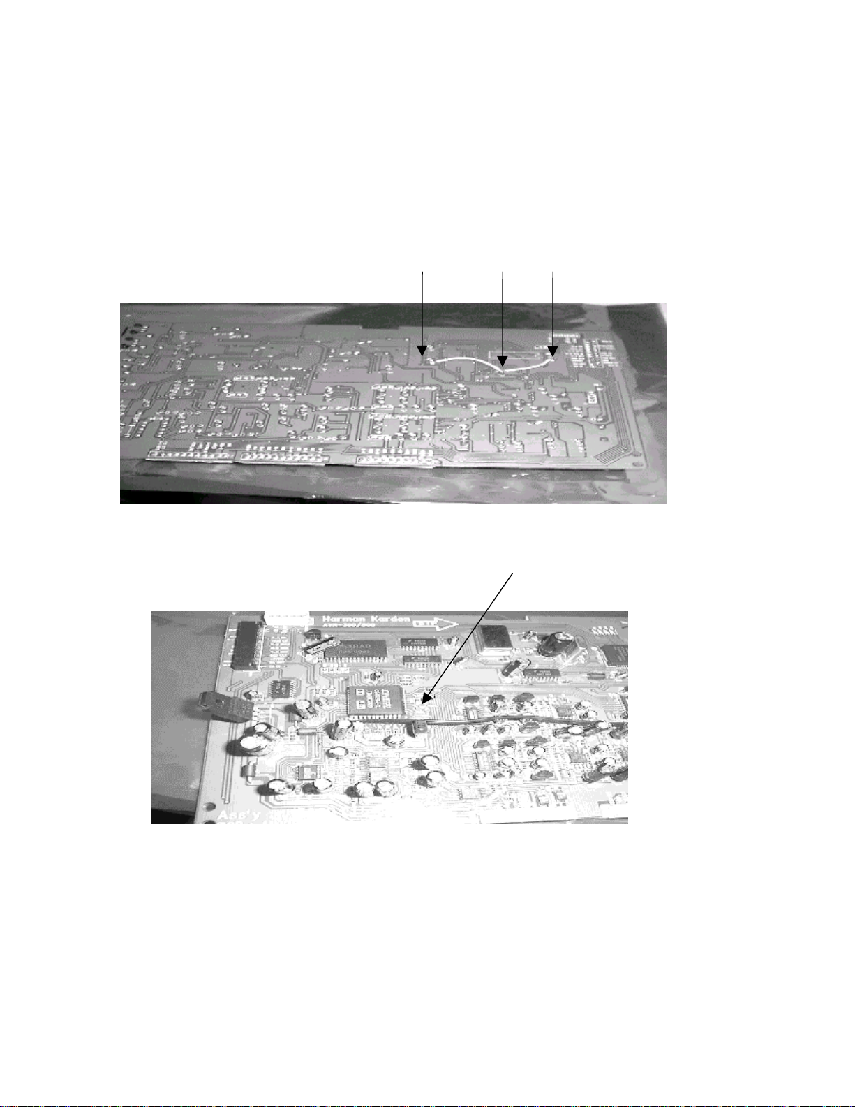
9) Ground Reinforcement:
Using an insulated 16AWG wire, Connect Negative sides of the following capacitors on the bottom side of the
PCB as shown below. Negative side of each cap will have a white mark on the component side of the PCB.
A. Negative polarity of C746 Elec Cap (1uF/50V) in the proximity of ROM IC709
B. Negative polarity of C749 Elec Cap (1uF/50V) in the proximity of IC708 DSP IC
C. Negative polarity of C744 Elec Cap (1uF/50V) in the proximity of IC710 74VHC574
C B A
2
10) Replace:
R756 & R755. Original parts may be 600W resistors, or Capacitors. Change both to 33W 1/10W
SMD resistors (h/k part#
11) Replace DSP PC Board back into its (3) receptacle plugs atop the MAIN PCB.
12) Replace all screws, braces, and any cable ties that were cut during disassembly. Before tightening the
screws, make sure all PCB’s and their RCA jacks are firmly seated in their respective holes in the rear
backplate. If using a power tool, use care and minimum effort to avoid damaging the various plastic
receptacles.
13) Plug both the 22 conductor ribbon cable and the 5 conductor molex cable back into their receptacles.
14) Replace the top cover and optical plugs.
15) Test unit by powering up the receiver and playing a source with DTS encoded material; confirm the complaint
of Random Noise or Erratic Output is no longer occurring.
292-33.2). See location below.
18
Page 19
harman/kardon Service Bulletin
Service bulletin # H/K2000-04 Rev1 February 2003
AVR500 MAJOR repair
To: All harman/kardon Service Centers AVR7000 MINOR repair
Models: AVR500/AVR7000
Subject: Noise in Logic 7 Mode
In the event you receive an AVR500 or AVR7000 receiver with the complaint “There is crackling, noise,
or distortion coming from my loudspeakers when my receiver is in the Logic 7 mode with certain
program material playing”, perform the following procedure:
AVR500 ONLY: REMOVAL AND MODIFICATION OF THE DSP BOARD (replace IC709 TRAD ROM-0001)
WARNING: FOLLOW PROPER STATIC CONTROL PROCEDURES and use caution during the removal of the
DSP board, and during installation of new IC709 to prevent damage.
1) Remove the top cover, (14) Black Phillips screws at the sides and rear of the unit.
2) Locate the DSP PC Board; Figure 1. Remove the two metal braces at the top of the unit. If necessary, cut
the cable ties attached to the braces to move any wires away from the area.
3) Pull the white 22 conductor ribbon cable at the rear of the DSP PC Board straight out of its receptacle.
4) Unplug the white 5 conductor molex cable at the top of the DSP PC Board.
5) Remove the (33) plated Phillips screws on the left side of the rear backplate; see Figure 2. Do not remove
any additional screws on the right side. If using a power tool, use care and minimum effort to avoid
damaging the various plastic receptacles.
6) Remove all three black plastic plugs that cover the optical inputs at the rear of the DSP PC Board.
7) Pull on the left side of the rear backplate, away from the receiver chassis; you should be able to pull it away
enough to allow the DSP PC Board to be pulled straight up and out of the receiver.
8) Unsolder IC709 TRAD ROM-0001 and replace with hk part# J21310030011. See illustration on following
page for location on PCB.
Warranty labor rate:
Model Serial Number
120V
AVR500
AVR500
TH0002-01000
To
TH0002-14977
TH0002-14978 or
higher
Serial Number
230V RDS
TH0006-01000
To
TH0006-05105
TH0006-05106 or
higher
STATUS
Noise in Logic 7 Mode
Modified by factory
19
ACTION
Replace IC709
TRAD ROM-0001
NONE REQUIRED
Page 20
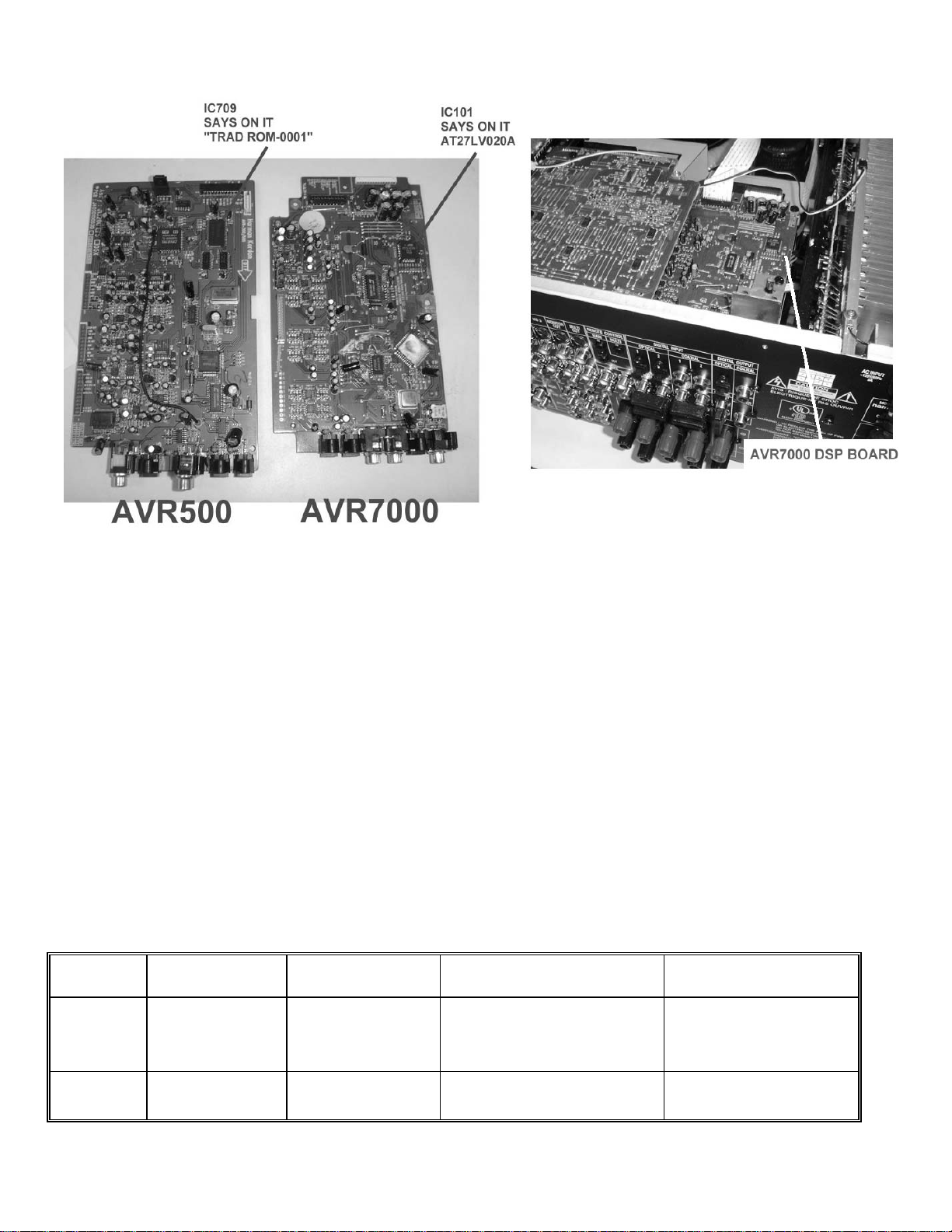
Location of IC upgrade for the AVR500/AVR7000:
9) Replace DSP PC Board back into its (3) receptacle plugs atop the MAIN PCB.
10) Replace all screws, braces, and any cable ties that were cut during disassembly. Before tightening the
screws, make sure all PCB’s and their RCA jacks are firmly seated in their respective holes in the rear
backplate. If using a power tool, use care and minimum effort to avoid damaging the various plastic
receptacles.
11) Plug both the 22 conductor ribbon cable and the 5 conductor molex cable back into their receptacles.
12) Replace the top cover and optical plugs.
13) Test unit by powering up the receiver and playing a music source in the Logic 7 mode.
AVR7000 ONLY: MODIFICATION OF THE DSP BOARD (replace IC101 AT27LV020A)
WARNING: FOLLOW PROPER STATIC CONTROL PROCEDURES and use caution during the installation of
new IC101 to prevent damage.
1) Remove the top cover, (16) Black Phillips screws at the sides and rear of the unit.
2) Locate the DSP PC Board and IC101 with the illustrations above.
3) Unsolder IC101 AT27LV020A and replace with hk part# 55172540AVR7000. See illustration above for
location on PCB.
4) Replace top cover and all Phillips screws.
5) Test unit by powering up the receiver and playing a music source in the Logic 7 mode.
Model Serial Number
120V
AVR7000
AVR7000
TH0003-01000
To
TH0003-05222
TH0003-05223
Or higher
Serial Number
230V RDS
Modified by factory
Modified by factory
STATUS
Noise in Logic 7 Mode
Modified by factory
NONE REQUIRED
ACTION
Replace IC101
AT27LV020A
20
Page 21
harman/kardon Service Bulletin
Service bulletin # H/K2000-05 May 2000 Warranty labor rate: MAJOR repair
To: All harman/kardon Service Centers
Models: AVR300, AVR500
Subject: Volume Level Changes
On early versions of the AVR300 or AVR500 the volume level may change by itself, or when the volume knob
is tapped. This may happen on an occasional random basis and depends on where the volume control knob is
positioned after a volume adjustment. During a running production change, new volume encoders were
installed.
In the event you receive an AVR300 or AVR500 with the complaint “The volume on my receiver
changes by itself”, perform the following procedure:
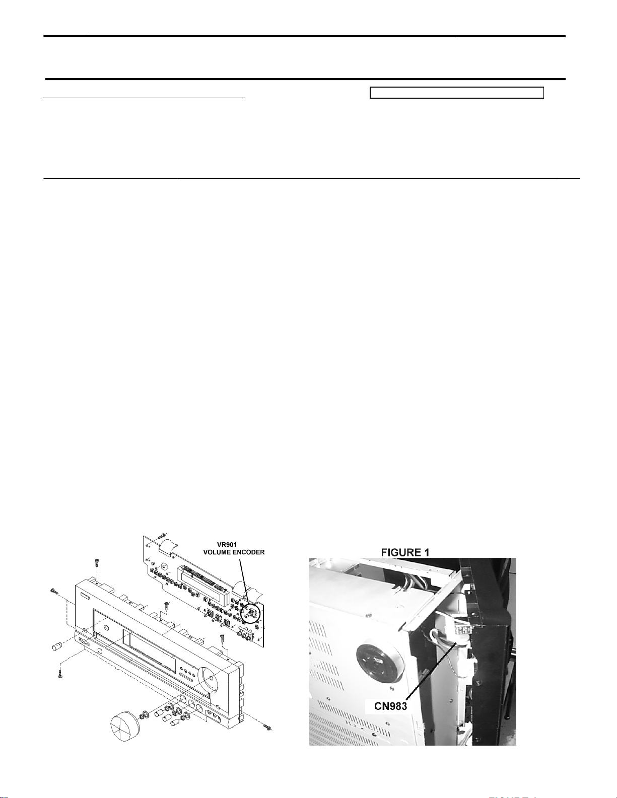
REPLACE VR901 VOLUME ENCODER
1) Remove the top cover, (14) Black Phillips screws.
2) Remove the (11) Black Phillips screws holding the plastic front panel to the chassis.
3) Remove the single Phillips screw on both right & left side of the chassis with a dual black ground wire.
4) Remove the volume, bass, treble and balance knobs by pulling them straight off.
5) Remove the single nut holding the volume encoder to the front panel.
6) Pull the loaded front panel off the chassis; cut any plastic cable ties necessary to fully disengage it
7) Lift and set the receiver on its right side for the remainder of the procedure.
8) Remove molex connector CN983 at the power switch; see Figure 1.
9) Pull the front panel as far away as the remaining connecting wires will allow.
10) Unsolder the connections at the rear of the front PCB to the volume encoder.
11) Using a “stubby” Phillips screwdriver, remove the (19) Black Phillips screws holding the front PCB to the
front panel; two plated screws at the rear of the headphone jack also must be removed.
12) Pull the front PCB away from the front panel.
13) Remove and replace the volume encoder with h/k part# J32612050102; resolder the new encoder in place.
14) Replace the front PCB and reassemble the receiver in reverse order, following the instructions above.
Replace all cable ties that were cut, and reattach any connectors that were unplugged. Make sure the two
ground wires on both sides of the receiver are reattached.
15) Power up receiver, and test volume control to assure it no longer changes settings by itself, or when the
volume knob is tapped.
21
Page 22

Models: AVR300, AVR500 Subject: Volume Level Changes
Model Serial Number
120V
AVR300
AVR500
AVR300
AVR500
TH0001-01000
To
TH0001-08402
TH0002-01000
To
TH0002-05565
TH0001-08403
Or higher
TH0002-05566
Or higher
Serial Number
230V RDS STATUS ACTION
TH0005-01000
To
TH0005-01001
TH0006-01000
To
TH0006-01001
TH0005-01002
Or higher
TH0006-01002
Or higher
Volume level changes by
itself or when volume
knob is tapped
Modified by factory NONE REQUIRED
Change VR901
Rotary encoder
22
Page 23
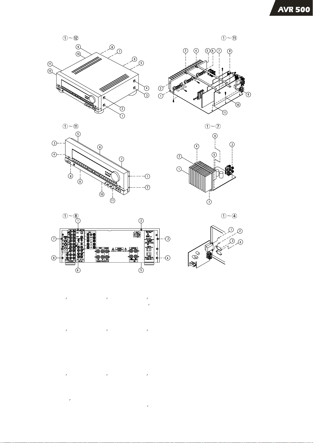
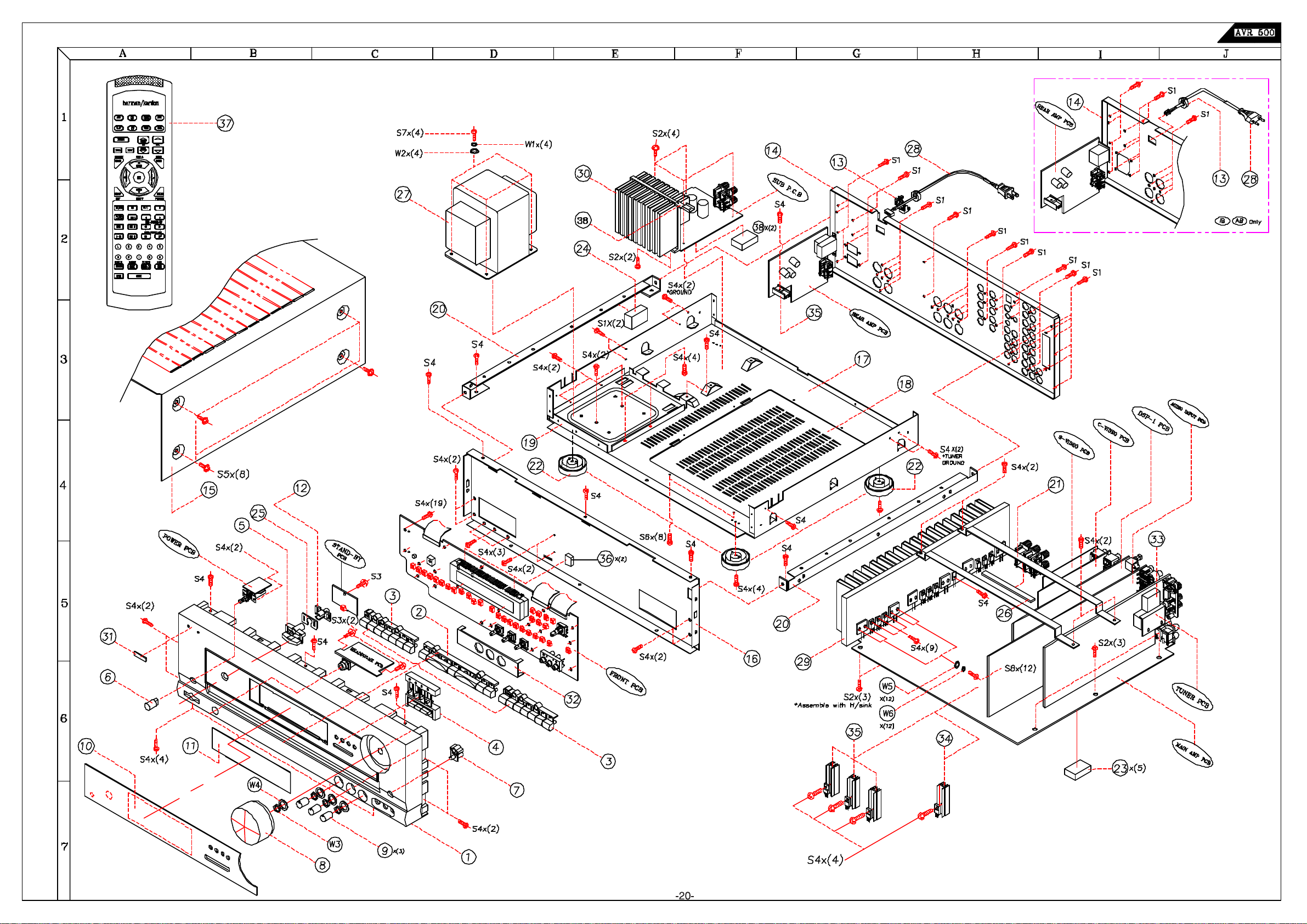
DISASSEMBLY PROCEDUREDISASSEMBLY PROCEDURE
1. Removingthe top cover, and
Removescrews
2. Removingthe front panel, and
Removescrews
4. Removingthe main PCBblock, and
Removescrews
5. Removingthe power PCBblock, and
Remove
3. Removingthe rear panel, and
Removescrews
MAIN AMP PCB BLOCKMAIN AMP PCB BLOCK
1. Removeall of the screwson Rearpanel.
2. Removethe Rearpanel.
3. RemovePCBBrk t and Guide
4. Removeall of the screwsthat connect with main Assy.
5. Removethe Main PCBblock.
POWER PCB BLOCKPOWER PCB BLOCK
1. RemovePCBBrk t and Guide
2. Remove4 screwsfor Power PCBmounting
3. Removethe POWERPCBblock.
SUB PCB BLOCKSUB PCB BLOCK
1. Remove4 screwson Rearpanel.
2. Removethe Rearpanel.
3. RemovePCBBrk t and Guide
4. Removethe SUBPCBblock.
Brk t from Main Assy.
Brk t from Main Assy.
Brk t from Main Assy.
6. Removingthe sub PCBblock, and
Removescrews
FRONT PCB BLOCKFRONT PCB BLOCK
1. RemoveMain
2. Removevolume and rotary knob from the front
3. Removeall of the screwson back sideof Front function PCB.
4. Removethe Front function PCB.
Assy.
Assy.
23
Page 24
24
Page 25
25
Page 26
26
Page 27
B C D E F G H I JA
27
1
2
3
4
5
6
7
Page 28
B C D E F G H I JA
28
1
2
3
4
5
6
7
Page 29
B C D E F G H I JA
29
1
2
3
4
5
6
7
Page 30

B C D E F G H I JA
30
1
2
3
4
5
6
7
Page 31
B C D E F G H I JA
31
1
2
3
4
5
6
7
Page 32

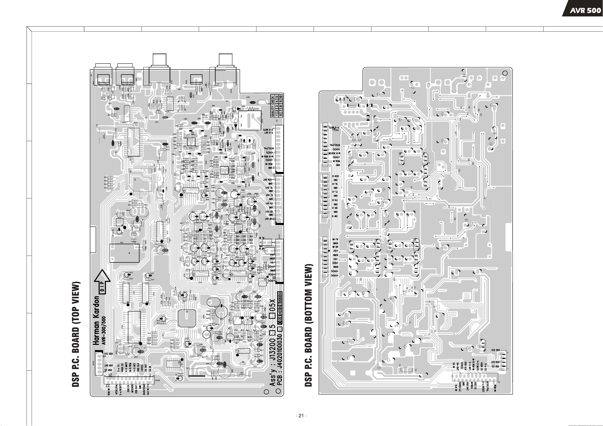
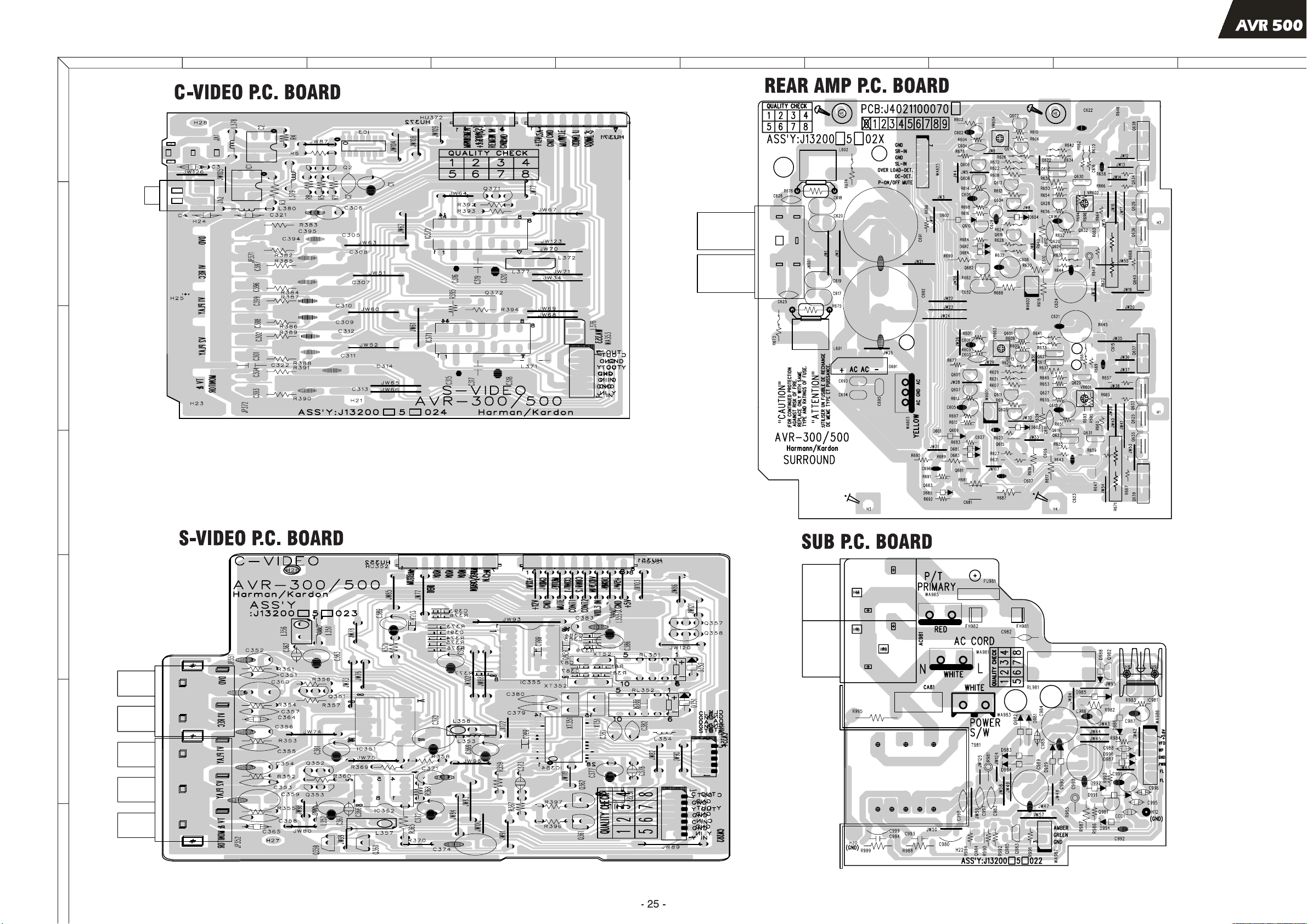
ELECTRIC PART LIST(500Serise) DSP P.C BOARD
32
REF NO. PART NO. DESCRIPTION REF NO. PART NO. DESCRIPTION
J1320045205X DSP P.C. BOARD
J1320045105X DSP P.C. BOARD
IB
BK L 704 J2631200010X HC3550 9.4ohm AXIAL
INTEGRATED CIRCUITs
IC 1 J2142930002X 74VHCT04SJX HEX INVERT L 707 J2631200010X HC3550 9.4ohm AXIAL
IC 2 J2120012001X NJM4558M OP-AMP L 708 J2631200010X HC3550 9.4ohm AXIAL
IC 701 J2120012002X NJM072M OP-AMP L 709 J2631200010X HC3550 9.4ohm AXIAL
IC 702 J2120012002X NJM072M OP-AMP L 821 J2631200010X HC3550 9.4ohm AXIAL
IC 703 J2133926002X CS5360-KS A/D CONVERTER
IC 704 J2142930001X 74VHC153SJX MULTIPLEXER R 6 J2631300174X HB-1T2012-601 CHIP
IC 705 J2129012001X NJU6324M QUARTZ OSC R 7 J2631300174X HB-1T2012-601 CHIP
IC 706 J2136926001X CS8414-CS DIGITAL AUDIO Rx. R 13 J2631300184X HB-1T2012-202 CHIP
IC 707 J2142930003X 74VHCT244SJX OCTAL NON-INVERT R 14 J2631300174X HB-1T2012-601 CHIP
IC 708 J2135326003X CS492604D DECODER R 15 J2631300174X HB-1T2012-601 CHIP
IC 709 J2131003001X KM23C4000DG-8 ROM-0001 R 17 J2631300174X HB-1T2012-601 CHIP
IC 709 J2131328002X AT27C040-100JC ROM OTP R 18 J2631300174X HB-1T2012-601 CHIP
IC 710 J2142930004X 74VHCT574SJX OCTAL D-FILP FLOP R 19 J2631300174X HB-1T2012-601 CHIP
IC 711 J2142930004X 74VHCT574SJX OCTAL D-FILP FLOP R 109 J2631300174X HB-1T2012-601 CHIP
IC 712 J2132321002X HD404354A52H MCU-0002 R 731 J2631300174X HB-1T2012-601 CHIP
IC 712 J2132321001X HD407A435PH SUB-u-COM OTP R 732 J2631300174X HB-1T2012-601 CHIP
IC 713 J2133926003X CS4341-KS D/A CONVERTER R 734 J2631300174X HB-1T2012-601 CHIP
IC 714 J2133926003X CS4341-KS D/A CONVERTER R 755 J2631300174X HB-1T2012-601 CHIP
IC 715 J2133926003X CS4341-KS D/A CONVERTER R 756 J2631300174X HB-1T2012-601 CHIP
IC 716 J2120012002X NJM072M OP-AMP R 760 J2631300174X HB-1T2012-601 CHIP
IC 717 J2120012002X NJM072M OP-AMP R 767 J2631300174X HB-1T2012-601 CHIP
IC 718 J2120012002X NJM072M OP-AMP R 781 J2631300174X HB-1T2012-601 CHIP
IC 719 J2142930006X 74VHCU04MX HEX INVERT R 782 J2631300174X HB-1T2012-601 CHIP
IC 720 J2112504001X BA033T REGULATOR 3.3V R 785 J2631300174X HB-1T2012-601 CHIP
IC 722 J2120012001X NJM4558M OP-AMP R 799 J2631300174X HB-1T2012-601 CHIP
IC 723 J2120012001X NJM4558M OP-AMP R 800 J2631300174X HB-1T2012-601 CHIP
IC 724 J2120012001X NJM4558M OP-AMP R 817 J2631300174X HB-1T2012-601 CHIP
IC 725 J2120012001X NJM4558M OP-AMP R 818 J2631300174X HB-1T2012-601 CHIP
TRANSISTORs
Q 703 J2021000201X KTA1266-Y PNP R 853 J2631300174X HB-1T2012-601 CHIP
Q 704 J2021220101X KRC101M NPN R 854 J2631300174X HB-1T2012-601 CHIP
Q 705 J2021200101X KRA101M PNP R 869 J2631300174X HB-1T2012-601 CHIP
Q 706 J2021060001X KTD1302-B NPN R 870 J2631300174X HB-1T2012-601 CHIP
Q 707 J2021060001X KTD1302-B NPN
Q 708 J2021220101X KRC101M NPN
Q 709 J2021200101X KRA101M PNP R 822 J3013561320X 1/5W CARBON 560W-J
Q 710 J2021060001X KTD1302-B NPN
Q 711 J2021060001X KTD1302-B NPN R 1 J3024101120X 1/10W CHIP 100W-J
Q 712 J2021220101X KRC101M NPN R 2 J3024222120X 1/10W CHIP 2K2W-J
Q 713 J2021200101X KRA101M PNP R 3 J3024473120X 1/10W CHIP 47KW-J
Q 714 J2021060001X KTD1302-B NPN R 4 J3024473120X 1/10W CHIP 47KW-J
Q 715 J2021060001X KTD1302-B NPN R 5 J3024222120X 1/10W CHIP 2K2W-J
Q 716 J2021220301X KRC103M NPN R 8 J3024472120X 1/10W CHIP 4K7W-J
DIODEs
D 705 J2221010100X 1SS133 SW. R 11 J3024474120X 1/10W CHIP 470KW-J
D 706 J2221010100X 1SS133 SW. R 12 J3024474120X 1/10W CHIP 470KW-J
COILs
L 701 J2616247020X AXIAL LAL02 47uH-K R 703 J3024103120X 1/10W CHIP 10KW-J
L 702 J2616247020X AXIAL LAL02 47uH-K R 704 J3024103120X 1/10W CHIP 10KW-J
J2616247020X AXIAL LAL02 47uH-K R 705 J3024103120X 1/10W CHIP 10KW-J
BEADs
L 705 J2631200010X HC3550 9.4ohm AXIAL
L 706 J2631200010X HC3550 9.4ohm AXIAL
R 839 J2631300174X HB-1T2012-601 CHIP
R 840 J2631300174X HB-1T2012-601 CHIP
RESISTORs
R 9 J3024472120X 1/10W CHIP 4K7W-J
R 10 J3024101120X 1/10W CHIP 100W-J
R 701 J3024203120X 1/10W CHIP 20KW-J
R 702 J3024203120X 1/10W CHIP 20KW-J
Page 33

REF NO. PART NO. DESCRIPTION REF NO. PART NO. DESCRIPTION
33
R 706 J3024103120X 1/10W CHIP 10KW-J R 788 J3024103120X 1/10W CHIP 10KW-J
R 707 J3024473120X 1/10W CHIP 47KW-J R 789 J3024103120X 1/10W CHIP 10KW-J
R 708 J3024473120X 1/10W CHIP 47KW-J R 790 J3024223120X 1/10W CHIP 22KW-J
R 709 J3024103120X 1/10W CHIP 10KW-J R 791 J3024223120X 1/10W CHIP 22KW-J
R 710 J3024103120X 1/10W CHIP 10KW-J R 792 J3024101120X 1/10W CHIP 100W-J
R 711 J3024151120X 1/10W CHIP 150W-J R 793 J3024103120X 1/10W CHIP 10KW-J
R 712 J3024151120X 1/10W CHIP 150W-J R 794 J3024103120X 1/10W CHIP 10KW-J
R 713 J3024151120X 1/10W CHIP 150W-J R 795 J3024122120X 1/10W CHIP 1K2W-J
R 714 J3024151120X 1/10W CHIP 150W-J R 796 J3024122120X 1/10W CHIP 1K2W-J
R 715 J3024100120X 1/10W CHIP 10W-J R 797 J3024203120X 1/10W CHIP 20KW-J
R 716 J3024100120X 1/10W CHIP 10W-J R 798 J3024203120X 1/10W CHIP 20KW-J
R 717 J3024101120X 1/10W CHIP 100W-J R 801 J3024473120X 1/10W CHIP 47KW-J
R 718 J3024101120X 1/10W CHIP 100W-J R 802 J3024473120X 1/10W CHIP 47KW-J
R 719 J3024750120X 1/10W CHIP 75W-J R 804 J3024561120X 1/10W CHIP 560W-J
R 720 J3024750120X 1/10W CHIP 75W-J R 805 J3024561120X 1/10W CHIP 560W-J
R 735 J3024471120X 1/10W CHIP 470W-J R 806 J3024103120X 1/10W CHIP 10KW-J
R 736 J3024103120X 1/10W CHIP 10KW-J R 807 J3024103120X 1/10W CHIP 10KW-J
R 737 J3024103120X 1/10W CHIP 10KW-J R 808 J3024223120X 1/10W CHIP 22KW-J
R 738 J3024103120X 1/10W CHIP 10KW-J R 809 J3024223120X 1/10W CHIP 22KW-J
R 739 J3024103120X 1/10W CHIP 10KW-J R 810 J3024101120X 1/10W CHIP 100W-J
R 740 J3024103120X 1/10W CHIP 10KW-J R 811 J3024103120X 1/10W CHIP 10KW-J
R 741 J3024103120X 1/10W CHIP 10KW-J R 812 J3024103120X 1/10W CHIP 10KW-J
R 742 J3024103120X 1/10W CHIP 10KW-J R 813 J3024122120X 1/10W CHIP 1K2W-J
R 743 J3024103120X 1/10W CHIP 10KW-J R 814 J3024122120X 1/10W CHIP 1K2W-J
R 744 J3024103120X 1/10W CHIP 10KW-J R 815 J3024203120X 1/10W CHIP 20KW-J
R 745 J3024103120X 1/10W CHIP 10KW-J R 816 J3024203120X 1/10W CHIP 20KW-J
R 746 J3024103120X 1/10W CHIP 10KW-J R 819 J3024473120X 1/10W CHIP 47KW-J
R 747 J3024472120X 1/10W CHIP 4K7W-J R 820 J3024473120X 1/10W CHIP 47KW-J
R 748 J3024473120X 1/10W CHIP 47KW-J R 827 J3024123120X 1/10W CHIP 12KW-J
R 749 J3024473120X 1/10W CHIP 47KW-J R 828 J3024123120X 1/10W CHIP 12KW-J
R 750 J3024473120X 1/10W CHIP 47KW-J R 829 J3024223120X 1/10W CHIP 22KW-J
R 751 J3024473120X 1/10W CHIP 47KW-J R 831 J3024224120X 1/10W CHIP 220KW-J
R 752 J3024100120X 1/10W CHIP 10W-J R 832 J3024224120X 1/10W CHIP 220KW-J
R 753 J3024222120X 1/10W CHIP 2K2W-J R 833 J3024123120X 1/10W CHIP 12KW-J
R 754 J3024103120X 1/10W CHIP 10KW-J R 834 J3024123120X 1/10W CHIP 12KW-J
R 757 J3024103120X 1/10W CHIP 10KW-J R 835 J3024123120X 1/10W CHIP 12KW-J
R 758 J3024472120X 1/10W CHIP 4K7W-J R 836 J3024123120X 1/10W CHIP 12KW-J
R 759 J3024103120X 1/10W CHIP 10KW-J R 837 J3024473120X 1/10W CHIP 47KW-J
R 761 J3024105120X 1/10W CHIP 1MW-J R 838 J3024473120X 1/10W CHIP 47KW-J
R 763 J3024473120X 1/10W CHIP 47KW-J R 845 J3024123120X 1/10W CHIP 12KW-J
R 764 J3024222120X 1/10W CHIP 2K2W-J R 846 J3024123120X 1/10W CHIP 12KW-J
R 765 J3024182120X 1/10W CHIP 1K8W-J R 847 J3024223120X 1/10W CHIP 22KW-J
R 766 J3024181120X 1/10W CHIP 180W-J R 848 J3024223120X 1/10W CHIP 22KW-J
R 768 J3024561120X 1/10W CHIP 560W-J R 849 J3024101120X 1/10W CHIP 100W-J
R 769 J3024561120X 1/10W CHIP 560W-J R 850 J3024101120X 1/10W CHIP 100W-J
R 770 J3024103120X 1/10W CHIP 10KW-J R 851 J3024224120X 1/10W CHIP 220KW-J
R 771 J3024103120X 1/10W CHIP 10KW-J R 852 J3024224120X 1/10W CHIP 220KW-J
R 772 J3024223120X 1/10W CHIP 22KW-J R 859 J3024123120X 1/10W CHIP 12KW-J
R 773 J3024223120X 1/10W CHIP 22KW-J R 860 J3024242120X 1/10W CHIP 2K4W-J
R 774 J3024101120X 1/10W CHIP 100W-J R 861 J3024223120X 1/10W CHIP 22KW-J
R 775 J3024103120X 1/10W CHIP 10KW-J R 862 J3024243120X 1/10W CHIP 24KW-J
R 776 J3024103120X 1/10W CHIP 10KW-J R 863 J3024224120X 1/10W CHIP 220KW-J
R 777 J3024122120X 1/10W CHIP 1K2W-J R 864 J3024224120X 1/10W CHIP 220KW-J
R 778 J3024122120X 1/10W CHIP 1K2W-J R 865 J3024101120X 1/10W CHIP 100W-J
R 779 J3024203120X 1/10W CHIP 20KW-J R 866 J3024101120X 1/10W CHIP 100W-J
R 780 J3024203120X 1/10W CHIP 20KW-J R 867 J3024203120X 1/10W CHIP 20KW-J
R 783 J3024473120X 1/10W CHIP 47KW-J R 868 J3024203120X 1/10W CHIP 20KW-J
R 784 J3024473120X 1/10W CHIP 47KW-J R 930 J3024223120X 1/10W CHIP 22KW-J
R 786 J3024561120X 1/10W CHIP 560W-J
R 787 J3024561120X 1/10W CHIP 560W-J
Page 34

REF NO. PART NO. DESCRIPTION REF NO. PART NO. DESCRIPTION
34
CAPACITORs
C 6 J3442110041X ELEC/CHIP 16V 10uF-K C 828 J3470147041X ELEC 25V 47uF-M
C 7 J3442110041X ELEC/CHIP 16V 10uF-K C 832 J3470110971X ELEC 50V 1uF-M
C 3 J3471610971X ELEC 50V 1uF-M C 836 J3470110071X ELEC 50V 10uF-M
C 4 J3471622041X ELEC 25V 22uF-M C 839 J3470110216X ELEC 6.3V 1000uF-M
C 701 J3470110071X ELEC 50V 10uF-M C 843 J3471647971X ELEC 50V 4.7uF-M
C 702 J3470110071X ELEC 50V 10uF-M C 844 J3471647971X ELEC 50V 4.7uF-M
C 711 J3470147041X ELEC 25V 47uF-M C 845 J3471647971X ELEC 50V 4.7uF-M
C 712 J3470147041X ELEC 25V 47uF-M C 846 J3471647971X ELEC 50V 4.7uF-M
C 715 J3470110971X ELEC 50V 1uF-M C 847 J3470147041X ELEC 25V 47uF-M
C 717 J3470110971X ELEC 50V 1uF-M C 848 J3470147041X ELEC 25V 47uF-M
C 727 J3470110216X ELEC 6.3V 1000uF-M C 853 J3471647971X ELEC 50V 4.7uF-M
C 729 J3471610971X ELEC 50V 1uF-M C 854 J3471647971X ELEC 50V 4.7uF-M
C 731 J3470110216X ELEC 6.3V 1000uF-M C 855 J3470147041X ELEC 25V 47uF-M
C 735 J3470110971X ELEC 50V 1uF-M C 856 J3470147041X ELEC 25V 47uF-M
C 738 J3470110216X ELEC 6.3V 1000uF-M C 861 J3471647971X ELEC 50V 4.7uF-M
C 741 J3470110971X ELEC 50V 1uF-M C 862 J3471647971X ELEC 50V 4.7uF-M
C 742 J3471610971X ELEC 50V 1uF-M C 863 J3471647971X ELEC 50V 4.7uF-M
C 744 J3471610971X ELEC 50V 1uF-M C 864 J3471610031X ELEC 16V 10uF-M
C 746 J3470110971X ELEC 50V 1uF-M C 865 J3471610031X ELEC 16V 10uF-M
C 749 J3471610971X ELEC 50V 1uF-M C 866 J3470147041X ELEC 25V 47uF-M
C 750 J3471610971X ELEC 50V 1uF-M C 867 J3470147041X ELEC 25V 47uF-M
C 753 J3471610971X ELEC 50V 1uF-M C 872 J3470110971X ELEC 50V 1uF-M
C 755 J3471647031X ELEC 16V 47uF-M
C 756 J3471622971X ELEC 50V 2.2uF-M C 11 J3523104540X CERA/DISC F 25V 0.1uF-Z
C 758 J3471610971X ELEC 50V 1uF-M C 840 J3523104540X CERA/DISC F 25V 0.1uF-Z
C 761 J3470110971X ELEC 50V 1uF-M
C 763 J3470110971X ELEC 50V 1uF-M C 2 J3525104540X CERA/CHIP F 25V 0.1uF-Z
C 766 J3471610971X ELEC 50V 1uF-M C 5 J3525103170X CERA/CHIP B 50V 0.01uF-K
C 768 J3471610971X ELEC 50V 1uF-M C 8 J3515101270X CERA/CHIP CH 50V 100pF-J
C 770 J3471610971X ELEC 50V 1uF-M C 9 J3515101270X CERA/CHIP CH 50V 100pF-J
C 771 J3471633971X ELEC 50V 3.3uF-M C 10 J3515101270X CERA/CHIP CH 50V 100pF-J
C 772 J3471633971X ELEC 50V 3.3uF-M C 12 J3515101270X CERA/CHIP CH 50V 100pF-J
C 775 J3471610031X ELEC 16V 10uF-M C 13 J3515101270X CERA/CHIP CH 50V 100pF-J
C 776 J3471610031X ELEC 16V 10uF-M C 703 J3525104540X CERA/CHIP F 25V 0.1uF-Z
C 781 J3471610031X ELEC 16V 10uF-M C 704 J3525104540X CERA/CHIP F 25V 0.1uF-Z
C 782 J3471610031X ELEC 16V 10uF-M C 705 J3515470270X CERA/CHIP CH 50V 47pF-J
C 783 J3470147041X ELEC 25V 47uF-M C 706 J3515470270X CERA/CHIP CH 50V 47pF-J
C 784 J3470147041X ELEC 25V 47uF-M C 707 J3515100270X CERA/CHIP CH 50V 10pF-D
C 788 J3471610971X ELEC 50V 1uF-M C 708 J3515100270X CERA/CHIP CH 50V 10pF-D
C 790 J3471610971X ELEC 50V 1uF-M C 709 J3525222170X CERA/CHIP B 50V 2200pF-K
C 792 J3471610971X ELEC 50V 1uF-M C 710 J3525222170X CERA/CHIP B 50V 2200pF-K
C 793 J3471633971X ELEC 50V 3.3uF-M C 713 J3525104540X CERA/CHIP F 25V 0.1uF-Z
C 794 J3471633971X ELEC 50V 3.3uF-M C 714 J3525104540X CERA/CHIP F 25V 0.1uF-Z
C 797 J3471610031X ELEC 16V 10uF-M C 716 J3525104540X CERA/CHIP F 25V 0.1uF-Z
C 798 J3471610031X ELEC 16V 10uF-M C 718 J3525104540X CERA/CHIP F 25V 0.1uF-Z
C 803 J3471610031X ELEC 16V 10uF-M C 719 J3525103170X CERA/CHIP B 50V 0.01uF-K
C 804 J3471610031X ELEC 16V 10uF-M C 720 J3525104540X CERA/CHIP F 25V 0.1uF-Z
C 805 J3470147041X ELEC 25V 47uF-M C 721 J3525104540X CERA/CHIP F 25V 0.1uF-Z
C 806 J3470147041X ELEC 25V 47uF-M C 722 J3525103170X CERA/CHIP B 50V 0.01uF-K
C 810 J3471610971X ELEC 50V 1uF-M C 723 J3525104540X CERA/CHIP F 25V 0.1uF-Z
C 812 J3471610971X ELEC 50V 1uF-M C 724 J3525104540X CERA/CHIP F 25V 0.1uF-Z
C 814 J3471610971X ELEC 50V 1uF-M C 725 J3525103170X CERA/CHIP B 50V 0.01uF-K
C 815 J3471633971X ELEC 50V 3.3uF-M C 726 J3525103170X CERA/CHIP B 50V 0.01uF-K
C 816 J3471633971X ELEC 50V 3.3uF-M C 728 J3525104540X CERA/CHIP F 25V 0.1uF-Z
C 819 J3471610031X ELEC 16V 10uF-M C 730 J3525104540X CERA/CHIP F 25V 0.1uF-Z
C 820 J3471610031X ELEC 16V 10uF-M C 732 J3525104540X CERA/CHIP F 25V 0.1uF-Z
C 825 J3471610031X ELEC 16V 10uF-M C 733 J3515150270X CERA/CHIP CH 50V 15pF-J
C 826 J3471610031X ELEC 16V 10uF-M C 734 J3525103170X CERA/CHIP B 50V 0.01uF-K
C 827 J3470147041X ELEC 25V 47uF-M
C 834 J3470110971X ELEC 50V 1uF-M
Page 35

REF NO. PART NO. DESCRIPTION REF NO. PART NO. DESCRIPTION
35
C 736 J3525104540X CERA/CHIP F 25V 0.1uF-Z C 1 J3681224731X MET POLYCARBO 63V 0.22uF-J
C 739 J3525104540X CERA/CHIP F 25V 0.1uF-Z C 737 J3640683220X MET POLY/RA 63V 0.068uF-J
C 740 J3525104540X CERA/CHIP F 25V 0.1uF-Z
C 743 J3525104540X CERA/CHIP F 25V 0.1uF-Z
C 745 J3525104540X CERA/CHIP F 25V 0.1uF-Z HU 1 J4423341160X 2.5mm 11P JE605-11
C 747 J3525104540X CERA/CHIP F 25V 0.1uF-Z HU 720 J4423341160X 2.5mm 11P JE605-11
C 748 J3525104540X CERA/CHIP F 25V 0.1uF-Z HU 721 J4423341060X 2.5mm 10P JE605-10
C 751 J3525104540X CERA/CHIP F 25V 0.1uF-Z WA 702 J4422112220X 1.25mm 22P 8370-227
C 752 J3525104540X CERA/CHIP F 25V 0.1uF-Z WA 703 J4420040500X 2.5mm 5P 5267-05A
C 754 J3525104540X CERA/CHIP F 25V 0.1uF-Z
C 757 J3525104540X CERA/CHIP F 25V 0.1uF-Z
C 759 J3515220270X CERA/CHIP CH 50V 22pF X 1 J43199011729 1P,1007#22(HI-WAP),170m/m
C 760 J3515220270X CERA/CHIP CH 50V 22pF
C 762 J3525104540X CERA/CHIP F 25V 0.1uF-Z
C 764 J3525104540X CERA/CHIP F 25V 0.1uF-Z JA 701 J2123806001X TORX178A OPTIC Rx
C 765 J3525104540X CERA/CHIP F 25V 0.1uF-Z JA 702 J2123806001X TORX178A OPTIC Rx
C 767 J3525104540X CERA/CHIP F 25V 0.1uF-Z JA 703 J44302201101 JW-1609RS
C 769 J3525104540X CERA/CHIP F 25V 0.1uF-Z JA 704 J2123806002X TOTX178 OPTIC Tx
C 773 J3525123170X CERA/CHIP B 50V 0.012uF-K JA 705 J44302101102 JW-1409S
C 774 J3525123170X CERA/CHIP B 50V 0.012uF-K RL 701 J5513300002X P-12 MEISEI 12V RELAY
C 777 J3525562170X CERA/CHIP B 50V 5600pF-K X 701 J3914010015X 12.288MHz SCO-K1-12288 OSC
C 778 J3525562170X CERA/CHIP B 50V 5600pF-K X 702 J3913010045X 5MHz 30pF X-TAL
C 779 J3515221270X CERA/CHIP CH 50V 220pF-J
C 780 J3515221270X CERA/CHIP CH 50V 220pF-J
C 785 J3525104540X CERA/CHIP F 25V 0.1uF-Z
C 786 J3525104540X CERA/CHIP F 25V 0.1uF-Z
C 787 J3525104540X CERA/CHIP F 25V 0.1uF-Z
C 789 J3525104540X CERA/CHIP F 25V 0.1uF-Z
C 791 J3525104540X CERA/CHIP F 25V 0.1uF-Z
C 795 J3525123170X CERA/CHIP B 50V 0.012uF-K
C 796 J3525123170X CERA/CHIP B 50V 0.012uF-K
C 799 J3525562170X CERA/CHIP B 50V 5600pF-K
C 800 J3525562170X CERA/CHIP B 50V 5600pF-K
C 801 J3515221270X CERA/CHIP CH 50V 220pF-J
C 802 J3515221270X CERA/CHIP CH 50V 220pF-J
C 807 J3525104540X CERA/CHIP F 25V 0.1uF-Z
C 808 J3525104540X CERA/CHIP F 25V 0.1uF-Z
C 809 J3525104540X CERA/CHIP F 25V 0.1uF-Z
C 811 J3525104540X CERA/CHIP F 25V 0.1uF-Z
C 813 J3525104540X CERA/CHIP F 25V 0.1uF-Z
C 817 J3525123170X CERA/CHIP B 50V 0.012uF-K
C 818 J3525334540X CERA/CHIP F 25V 0.33uF-Z
C 821 J3525562170X CERA/CHIP B 50V 5600pF-K
C 822 J3525562170X CERA/CHIP B 50V 5600pF-K
C 823 J3515221270X CERA/CHIP CH 50V 220pF-J
C 824 J3515221270X CERA/CHIP CH 50V 220pF-J
C 829 J3525104540X CERA/CHIP F 25V 0.1uF-Z
C 830 J3525104540X CERA/CHIP F 25V 0.1uF-Z
C 831 J3525104540X CERA/CHIP F 25V 0.1uF-Z
C 833 J3525104540X CERA/CHIP F 25V 0.1uF-Z
C 835 J3525104540X CERA/CHIP F 25V 0.1uF-Z
C 837 J3525104540X CERA/CHIP F 25V 0.1uF-Z
C 838 J3525104540X CERA/CHIP F 25V 0.1uF-Z
C 849 J3525104540X CERA/CHIP F 25V 0.1uF-Z
C 850 J3525104540X CERA/CHIP F 25V 0.1uF-Z
C 857 J3525104540X CERA/CHIP F 25V 0.1uF-Z
C 858 J3525104540X CERA/CHIP F 25V 0.1uF-Z
C 868 J3525104540X CERA/CHIP F 25V 0.1uF-Z
C 869 J3525104540X CERA/CHIP F 25V 0.1uF-Z
C 871 J3525104540X CERA/CHIP F 25V 0.1uF-Z
WAFERs
WIREs
MISCELLANIES
2P RCA JACK
1P RCA JACK
Page 36

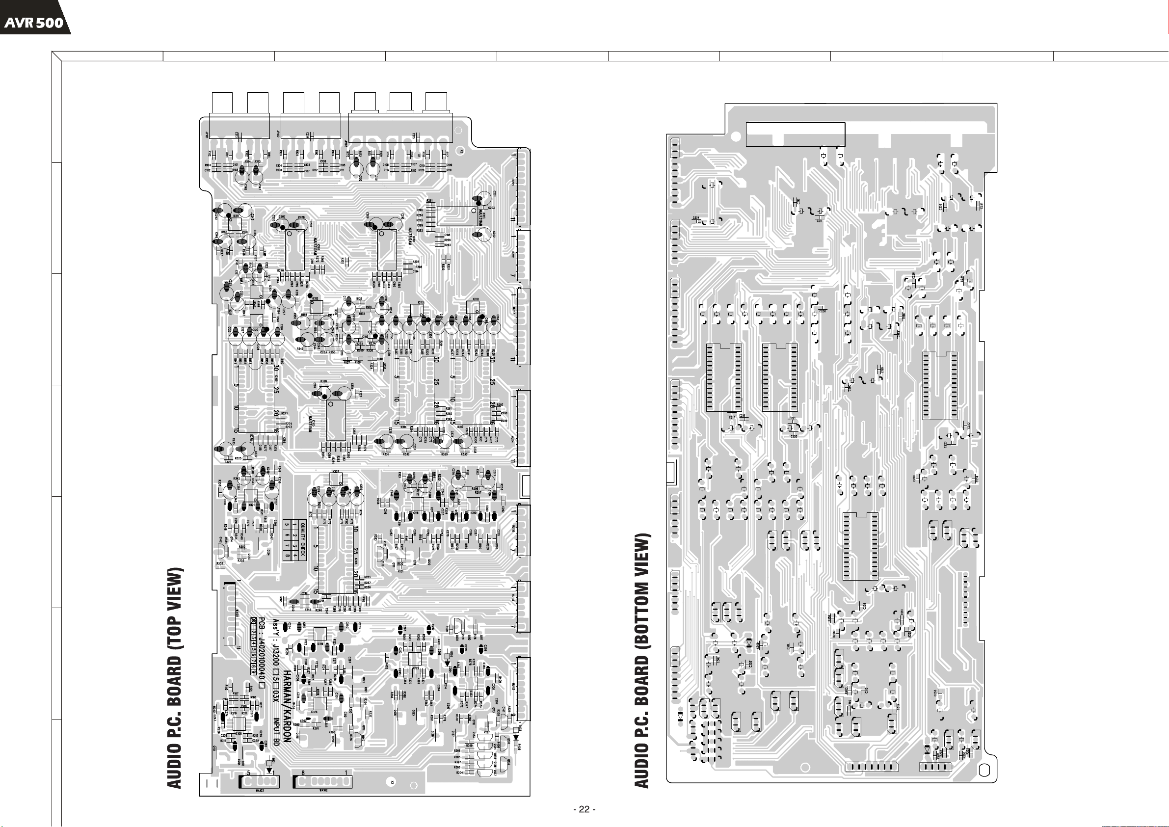
ELECTRIC PART LIST(500Serise) INPUT P.C. BOARD
TRANSISTORs
36
REF NO. PART NO. DESCRIPTION REF NO. PART NO. DESCRIPTION
J1320045203X
J1320045103X
INPUT P.C. BOARD
INPUT P.C. BOARD
INTEGRATED CIRCUITs
IC 101
J2121712002X NJU7312AM
IC 102
J2121712003X NJU7313AM
J2120012001X NJM4558M OP-AMP
IC 103
J2120012001X NJM4558M OP-AMP
IC 104
IC 105
J2121712001X NJU7311AM
IC 106
J2115211003X LC7536
J2120012001X NJM4558M OP-AMP
IC 107
J2120012001X NJM4558M OP-AMP
IC 108
IC 109
J2115211003X LC7536
J2120012001X NJM4558M OP-AMP
IC 110
J2120012001X NJM4558M OP-AMP
IC 111
J2120012001X NJM4558M OP-AMP
IC 112
IC 113
J2121712001X NJU7311AM
IC 114
J2115211003X LC7536
J2120012001X NJM4558M OP-AMP
IC 115
J2120012001X NJM4558M OP-AMP
IC 116
IC 117
J2115211003X LC7536
J2120012001X NJM4558M OP-AMP
IC 118
J2120012001X NJM4558M OP-AMP
IC 119
J2120012001X NJM4558M OP-AMP
IC 120
J2120012001X NJM4558M OP-AMP
IC 121
J2120012001X NJM4558M OP-AMP
IC 122
J2120012001X NJM4558M OP-AMP
IC 123
J2120012001X NJM4558M OP-AMP
IC 124
Q 110 J2021000201X KTA1266-Y PNP
Q 111 J2021000201X KTA1266-Y PNP
Q 112 J2021000201X KTA1266-Y PNP
Q 113 J2021000201X KTA1266-Y PNP
Q 114 J2021000201X KTA1266-Y PNP R 123
J20210600011 KTD1302-B NPN R 124
Q 115
J20210600011 KTD1302-B NPN
Q 116
J2021060001X KTD1302-B NPN
Q 117
J2021060001X KTD1302-B NPN
Q 118
J2021060001X KTD1302-B NPN
Q 119
J2021060001X KTD1302-B NPN R 129 J3024183120X
Q 120
J2021060001X KTD1302-B NPN
Q 121
J2021060001X KTD1302-B NPN
Q 122
J2021060001X KTD1302-B NPN
Q 123
J2021060001X KTD1302-B NPN
Q 124
J2021060001X KTD1302-B NPN
Q 125
J2021060001X KTD1302-B NPN
Q 126
J2021060001X KTD1302-B NPN
Q 127
J2021060001X KTD1302-B NPN
Q 128
J2021060001X KTD1302-B NPN
Q 129
J2021060001X KTD1302-B NPN R 139 J3024224120X
Q 130
Q 131
J2021220201X KRC102M
Q 132
J2021220201X KRC102M
Q 133
J2021200301X KRA103M
Q 134
J2021200301X KRA103M
Q 135
J2021200301X KRA103M
Q 136
J2021200301X KRA103M
Q 137
J2021200301X KRA103M
FUNC. SW. Q 142
FUNC. SW.
FUNC. SW.
ELEC. VR.
ELEC. VR.
FUNC. SW.
ELEC. VR.
ELEC. VR.
IB Q 138
BK Q 139
Q 140
Q 141
D 101
D 102
D 103
R 101
R 102
R 103
R 104
R 105
R 106
R 107
R 108
R 109
R 110
R 111
R 112
R 113
R 114
R 115
R 116
R 117
R 118 J3024331120X 1/10W CHIP 330W-J
R 119
R 120
R 121
R 122
R 125
R 126
R 127
R 128 J3024223120X 1/10W CHIP 22KW-J
R 130
R 131
R 132 J3024223120X 1/10W CHIP 22KW-J
R 133
R 134
R 135
R 136
R 137
R 138
NPN R 140 J3024224120X
NPN
PNP
PNP
PNP
PNP
PNP
R 141
R 142
R 143
R 144
R 145
R 146
J2021220101X KRC101M
J2021220101X KRC101M
J2021220101X KRC101M
J2021220101X KRC101M
J2021220101X KRC101M
NPN
NPN
NPN
NPN
NPN
DIODEs
J2221010100X 1SS133 SW.
J2221010100X 1SS133 SW.
J2221010100X 1SS133 SW.
RESISTORs
J3024331120X
J3024331120X
J3024474120X
J3024474120X
J3024331120X
J3024331120X
J3024474120X
J3024474120X
J3024331120X
J3024331120X
J3024474120X
J3024474120X
J3024331120X
J3024331120X
J3024474120X
J3024474120X
J3024331120X
J3024474120X
J3024474120X
J3024102120X
J3024433120X
J3024822120X 1/10W CHIP 8K2W-J
J3024822120X 1/10W CHIP 8K2W-J
J3024433120X
J3024331120X
J3024331120X
J3024331120X
J3024331120X
J3024101120X
J3024101120X
J3024474120X
J3024474120X
J3024101120X
J3024101120X
J3024101120X
J3024101120X
J3024474120X
J3024474120X
J3024101120X
J3024101120X
1/10W CHIP 330W-J
1/10W CHIP 330W-J
1/10W CHIP 470KW-J
1/10W CHIP 470KW-J
1/10W CHIP 330W-J
1/10W CHIP 330W-J
1/10W CHIP 470KW-J
1/10W CHIP 470KW-J
1/10W CHIP 330W-J
1/10W CHIP 330W-J
1/10W CHIP 470KW-J
1/10W CHIP 470KW-J
1/10W CHIP 330W-J
1/10W CHIP 330W-J
1/10W CHIP 470KW-J
1/10W CHIP 470KW-J
1/10W CHIP 330W-J
1/10W CHIP 470KW-J
1/10W CHIP 470KW-J
1/10W CHIP 1KW-J
1/10W CHIP 43KW-J
1/10W CHIP 43KW-J
1/10W CHIP 330W-J
1/10W CHIP 330W-J
1/10W CHIP 18KW-J
1/10W CHIP 330W-J
1/10W CHIP 330W-J
1/10W CHIP 100W-J
1/10W CHIP 100W-J
1/10W CHIP 470KW-J
1/10W CHIP 470KW-J
1/10W CHIP 100W-J
1/10W CHIP 100W-J
1/10W CHIP 220KW-J
1/10W CHIP 220KW-J
1/10W CHIP 100W-J
1/10W CHIP 100W-J
1/10W CHIP 470KW-J
1/10W CHIP 470KW-J
1/10W CHIP 100W-J
1/10W CHIP 100W-J
Page 37

REF NO. PART NO. DESCRIPTION REF NO. PART NO. DESCRIPTION
37
R 147 J3024224120X
R 148 J3024224120X
J3024101120X
R 149
J3024101120X
R 150
R 151 J3024224120X
R 152 J3024224120X
J3024101120X
R 153
J3024101120X
R 154
R 155 J3024224120X
R 156 J3024224120X
J3024101120X
R 157
J3024101120X
R 158
J3024474120X
R 159
J3024474120X
R 160
R 161
J3024152120X 1/10W CHIP 1K5W-J
R 162
J3024152120X 1/10W CHIP 1K5W-J
R 163 J3024224120X
R 164 J3024224120X
J3024101120X
R 165
J3024101120X
R 166
J3024474120X
R 167
J3024474120X
R 168
R 169
J3024152120X 1/10W CHIP 1K5W-J
R 170
J3024152120X 1/10W CHIP 1K5W-J
R 171 J3024224120X
R 172 J3024224120X
J3024101120X
R 173
J3024101120X
R 174
R 175 J3024224120X
R 176 J3024224120X
J3024101120X
R 177
J3024101120X
R 178
R 179 J3024224120X
R 180 J3024224120X
J3024101120X
R 181
J3024101120X
R 182
J3024101120X
R 183
J3024101120X
R 184
J3024101120X
R 185
J3024101120X
R 186
R 187
J3024104120X 1/10W CHIP 100KW-J R 252
R 188
J3024104120X 1/10W CHIP 100KW-J R 253
J3024222120X
R 189
J3024222120X
R 190
J3024222120X
R 191
J3024222120X
R 192
J3024102120X
R 193
J3024102120X
R 194
J3024102120X
R 195
J3024102120X
R 196
J3024102120X
R 197
J3024102120X
R 198
J3024102120X
R 199
R 200
J3024229120X 1/10W CHIP 2R2W-J R 268
R 201
J3024229120X 1/10W CHIP 2R2W-J R 269
J3024222120X
R 202
J3024222120X
R 203
J3024222120X
R 204
J3024222120X
R 205
R 206 J3024224120X
1/10W CHIP 220KW-J
1/10W CHIP 220KW-J
1/10W CHIP 100W-J
1/10W CHIP 100W-J
1/10W CHIP 220KW-J
1/10W CHIP 220KW-J
1/10W CHIP 100W-J R 213
1/10W CHIP 100W-J R 214
1/10W CHIP 220KW-J
1/10W CHIP 220KW-J
1/10W CHIP 100W-J R 217
1/10W CHIP 100W-J R 218
1/10W CHIP 470KW-J
1/10W CHIP 470KW-J
1/10W CHIP 220KW-J
1/10W CHIP 220KW-J
1/10W CHIP 100W-J
1/10W CHIP 100W-J
1/10W CHIP 470KW-J
1/10W CHIP 470KW-J
1/10W CHIP 220KW-J
1/10W CHIP 220KW-J R 237
1/10W CHIP 100W-J R 238
1/10W CHIP 100W-J
1/10W CHIP 220KW-J
1/10W CHIP 220KW-J R 241
1/10W CHIP 100W-J R 242
1/10W CHIP 100W-J
1/10W CHIP 220KW-J
1/10W CHIP 220KW-J R 245
1/10W CHIP 100W-J R 246
1/10W CHIP 100W-J R 247
1/10W CHIP 100W-J R 248
1/10W CHIP 100W-J R 249
1/10W CHIP 100W-J R 250
1/10W CHIP 100W-J R 251
1/10W CHIP 2K2W-J R 254
1/10W CHIP 2K2W-J R 255
1/10W CHIP 2K2W-J R 256
1/10W CHIP 2K2W-J
1/10W CHIP 1KW-J R 261
1/10W CHIP 1KW-J R 262
1/10W CHIP 1KW-J R 263
1/10W CHIP 1KW-J R 264
1/10W CHIP 1KW-J R 265
1/10W CHIP 1KW-J R 266
1/10W CHIP 1KW-J R 267
1/10W CHIP 2K2W-J R 270
1/10W CHIP 2K2W-J R 271
1/10W CHIP 2K2W-J R 272
1/10W CHIP 2K2W-J R 273
1/10W CHIP 220KW-J R 274
R 207 J3024224120X
R 208 J3024224120X
R 209 J3024224120X
R 210 J3024472120X
R 211 J3024472120X
R 212 J3024203120X
J3024101120X
J3024101120X
R 215 J3024224120X
R 216 J3024224120X
J3024101120X
J3024101120X
R 219 J3024224120X
R 220 J3024224120X
R 221 J3024224120X
R 222 J3024224120X
R 223 J3024224120X
R 224 J3024224120X
R 225 J3024224120X
R 226 J3024224120X
R 227 J3024224120X
R 228 J3024224120X
R 234
J3024822120X 1/10W CHIP 8K2W-J
R 235
J3024822120X 1/10W CHIP 8K2W-J
R 236
J3024123120X 1/10W CHIP 12KW-J
J3024101120X
J3024101120X
R 239 J3024224120X
R 240 J3024224120X
J3024101120X
J3024101120X
R 243 J3024224120X
R 244 J3024224120X
J3024479120X
J3024479120X
J3024479120X
J3024479120X
J3024479120X
J3024479120X
J3024479120X
J3024479120X
J3024479120X
J3024479120X
J3024479120X
J3024479120X
R 260
J3024123120X 1/10W CHIP 12KW-J
J3024102120X
J3024102120X
J3024102120X
J3024473120X
J3024473120X
J3024473120X
J3024102120X
J3024102120X
J3024102120X
J3024473120X
J3024473120X
J3024473120X
J3024102120X
J3024102120X
1/10W CHIP 220KW-J
1/10W CHIP 220KW-J
1/10W CHIP 220KW-J
1/10W CHIP 4K7W-J
1/10W CHIP 4K7W-J
1/10W CHIP 20KW-J
1/10W CHIP 100W-J
1/10W CHIP 100W-J
1/10W CHIP 220KW-J
1/10W CHIP 220KW-J
1/10W CHIP 100W-J
1/10W CHIP 100W-J
1/10W CHIP 220KW-J
1/10W CHIP 220KW-J
1/10W CHIP 220KW-J
1/10W CHIP 220KW-J
1/10W CHIP 220KW-J
1/10W CHIP 220KW-J
1/10W CHIP 220KW-J
1/10W CHIP 220KW-J
1/10W CHIP 220KW-J
1/10W CHIP 220KW-J
1/10W CHIP 100W-J
1/10W CHIP 100W-J
1/10W CHIP 220KW-J
1/10W CHIP 220KW-J
1/10W CHIP 100W-J
1/10W CHIP 100W-J
1/10W CHIP 220KW-J
1/10W CHIP 220KW-J
1/10W CHIP 4R7W-J
1/10W CHIP 4R7W-J
1/10W CHIP 4R7W-J
1/10W CHIP 4R7W-J
1/10W CHIP 4R7W-J
1/10W CHIP 4R7W-J
1/10W CHIP 4R7W-J
1/10W CHIP 4R7W-J
1/10W CHIP 4R7W-J
1/10W CHIP 4R7W-J
1/10W CHIP 4R7W-J
1/10W CHIP 4R7W-J
1/10W CHIP 1KW-J
1/10W CHIP 1KW-J
1/10W CHIP 1KW-J
1/10W CHIP 47KW-J
1/10W CHIP 47KW-J
1/10W CHIP 47KW-J
1/10W CHIP 1KW-J
1/10W CHIP 1KW-J
1/10W CHIP 1KW-J
1/10W CHIP 47KW-J
1/10W CHIP 47KW-J
1/10W CHIP 47KW-J
1/10W CHIP 1KW-J
1/10W CHIP 1KW-J
Page 38

REF NO. PART NO. DESCRIPTION REF NO. PART NO. DESCRIPTION
38
J3024102120X
R 275
J3024473120X
R 276
J3024473120X
R 277
J3024473120X
R 278
J3024102120X
R 279
J3024102120X
R 280
J3024102120X
R 281
J3024473120X
R 282
J3024473120X
R 283
J3024473120X
R 284
J3024102120X
R 285
J3024102120X
R 286
J3024102120X
R 287
J3024473120X
R 288
J3024473120X
R 289
J3024473120X
R 290
J3024102120X
R 291
J3024102120X
R 292
J3024102120X
R 293
J3024473120X
R 294
J3024473120X
R 295
J3024473120X
R 296
J3024102120X
R 297
J3024102120X
R 298
J3024102120X
R 299
J3024473120X
R 300
J3024473120X
R 301
J3024473120X
R 302
J3024102120X
R 303
J3024102120X
R 304
J3024102120X
R 305
J3024473120X
R 306
J3024473120X
R 307
J3024473120X
R 308
R 309 J3024203120X
R 310 J3024203120X
R 311 J3024203120X
R 312
J3024124120X 1/10W CHIP 120KW-J
R 313
J3024124120X 1/10W CHIP 120KW-J
J3024479120X
R 314
J3024479120X
R 315
J3024479120X
R 316
J3024479120X
R 317
J3024479120X
R 318
J3024479120X
R 319
J3024479120X
R 320
J3024479120X
R 321
J3024479120X
R 322
J3024479120X
R 323
J3024479120X
R 324
J3024479120X
R 325
J3024479120X
R 326
J3024479120X
R 327
J3024479120X
R 328
J3024479120X
R 329
J3024479120X
R 330
J3024479120X
R 331
J3024479120X
R 332
R 333 J3024183120X
J3024331120X
R 334
1/10W CHIP 1KW-J R 335
1/10W CHIP 47KW-J R 336 J3024223120X 1/10W CHIP 22KW-J
1/10W CHIP 47KW-J
1/10W CHIP 47KW-J R 338 J3024223120X 1/10W CHIP 22KW-J
1/10W CHIP 1KW-J
1/10W CHIP 1KW-J R 340
1/10W CHIP 1KW-J R 341
1/10W CHIP 47KW-J
1/10W CHIP 47KW-J
1/10W CHIP 47KW-J
1/10W CHIP 1KW-J
1/10W CHIP 1KW-J R 346
1/10W CHIP 1KW-J R 347
1/10W CHIP 47KW-J R 348 J3024333120X 1/10W CHIP 33KW-J
1/10W CHIP 47KW-J
1/10W CHIP 47KW-J
1/10W CHIP 1KW-J R 351 J3024333120X 1/10W CHIP 33KW-J
1/10W CHIP 1KW-J R 352
1/10W CHIP 1KW-J R 353
1/10W CHIP 47KW-J R 354 J3024223120X 1/10W CHIP 22KW-J
1/10W CHIP 47KW-J
1/10W CHIP 47KW-J R 356
1/10W CHIP 1KW-J R 357
1/10W CHIP 1KW-J R 358
1/10W CHIP 1KW-J R 359
1/10W CHIP 47KW-J R 360
1/10W CHIP 47KW-J R 361
1/10W CHIP 47KW-J
1/10W CHIP 1KW-J
1/10W CHIP 1KW-J R 364 J3024000120X 1/10W CHIP
1/10W CHIP 1KW-J R 365
1/10W CHIP 47KW-J R 366
1/10W CHIP 47KW-J
1/10W CHIP 47KW-J
1/10W CHIP 20KW-J R 371 J3024000120X 1/10W CHIP
1/10W CHIP 20KW-J R 372 J3024000120X 1/10W CHIP
1/10W CHIP 20KW-J R 373 J3024000120X 1/10W CHIP
1/10W CHIP 4R7W-J
1/10W CHIP 4R7W-J
1/10W CHIP 4R7W-J R 380
1/10W CHIP 4R7W-J R 381
1/10W CHIP 4R7W-J R 382
1/10W CHIP 4R7W-J R 383
1/10W CHIP 4R7W-J R 384
1/10W CHIP 4R7W-J R 385
1/10W CHIP 4R7W-J
1/10W CHIP 4R7W-J
1/10W CHIP 4R7W-J R 389
1/10W CHIP 4R7W-J R 390
1/10W CHIP 4R7W-J
1/10W CHIP 4R7W-J
1/10W CHIP 4R7W-J R 396
1/10W CHIP 4R7W-J R 397
1/10W CHIP 4R7W-J R 398
1/10W CHIP 4R7W-J R 399
1/10W CHIP 4R7W-J R 400
1/10W CHIP 18KW-J R 401
1/10W CHIP 330W-J R 402
J3024331120X
R 337 J3024183120X
R 339 J3024183120X
J3024101120X
J3024101120X
R 342 J3024224120X
R 343 J3024224120X
R 344 J3024224120X
R 345 J3024224120X
J3024102120X
J3024102120X
R 349
J3024752120X 1/10W CHIP 7K5W-J
R 350
J3024752120X 1/10W CHIP 7K5W-J
J3024331120X
J3024331120X
R 355 J3024183120X
J3024479120X
J3024479120X
J3024479120X
J3024479120X
J3024101120X
J3024101120X
R 362 J3024224120X
R 363 J3024224120X
J3024101120X
J3024101120X
R 367 J3024224120X
R 368 J3024224120X
R 375 J3024224120X
R 376 J3024224120X
R 378 J3024224120X
R 379 J3024224120X
J3024101120X
J3024101120X
J3024101120X
J3024101120X
J3024101120X
J3024101120X
R 386 J3024224120X
R 387 J3024224120X
J3024101120X
J3024101120X
R 391 J3024224120X
R 392 J3024224120X
J3024222120X
J3024222120X
J3024222120X
J3024222120X
J3024479120X
J3024479120X
J3024479120X
1/10W CHIP 330W-J
1/10W CHIP 18KW-J
1/10W CHIP 18KW-J
1/10W CHIP 100W-J
1/10W CHIP 100W-J
1/10W CHIP 220KW-J
1/10W CHIP 220KW-J
1/10W CHIP 220KW-J
1/10W CHIP 220KW-J
1/10W CHIP 1KW-J
1/10W CHIP 1KW-J
1/10W CHIP 330W-J
1/10W CHIP 330W-J
1/10W CHIP 18KW-J
1/10W CHIP 4R7W-J
1/10W CHIP 4R7W-J
1/10W CHIP 4R7W-J
1/10W CHIP 4R7W-J
1/10W CHIP 100W-J
1/10W CHIP 100W-J
1/10W CHIP 220KW-J
1/10W CHIP 220KW-J
1/10W CHIP 100W-J
1/10W CHIP 100W-J
1/10W CHIP 220KW-J
1/10W CHIP 220KW-J
1/10W CHIP 220KW-J
1/10W CHIP 220KW-J
1/10W CHIP 220KW-J
1/10W CHIP 220KW-J
1/10W CHIP 100W-J
1/10W CHIP 100W-J
1/10W CHIP 100W-J
1/10W CHIP 100W-J
1/10W CHIP 100W-J
1/10W CHIP 100W-J
1/10W CHIP 220KW-J
1/10W CHIP 220KW-J
1/10W CHIP 100W-J
1/10W CHIP 100W-J
1/10W CHIP 220KW-J
1/10W CHIP 220KW-J
1/10W CHIP 2K2W-J
1/10W CHIP 2K2W-J
1/10W CHIP 2K2W-J
1/10W CHIP 2K2W-J
1/10W CHIP 4R7W-J
1/10W CHIP 4R7W-J
1/10W CHIP 4R7W-J
0W-J
0W-J
0W-J
0W-J
Page 39

REF NO. PART NO. DESCRIPTION REF NO. PART NO. DESCRIPTION
39
J3024479120X
R 403
J3024479120X
R 404
R 405 J3024183120X
R 406 J3024183120X
1/10W CHIP 4R7W-J C 237
1/10W CHIP 4R7W-J C 240
1/10W CHIP 18KW-J C 241
1/10W CHIP 18KW-J C 242
CAPACITORs
C 117 J3470147971X ELEC 50V 4.7uF-M
C 118 J3470147971X ELEC 50V 4.7uF-M
J3470647931X ELEC 16V 4.7uF-M
C 119
J3470647931X ELEC 16V 4.7uF-M
C 120
C 121 J3470147971X ELEC 50V 4.7uF-M
C 122 J3470147971X ELEC 50V 4.7uF-M
J3470647931X ELEC 16V 4.7uF-M
C 123
J3470647931X ELEC 16V 4.7uF-M
C 124
J3470647931X ELEC 16V 4.7uF-M
C 125
J3470647931X ELEC 16V 4.7uF-M
C 126
J3470647931X ELEC 16V 4.7uF-M
C 127
J3470647931X ELEC 16V 4.7uF-M
C 128
J3470647931X ELEC 16V 4.7uF-M
C 129
J3470647931X ELEC 16V 4.7uF-M
C 130
J3470647931X ELEC 16V 4.7uF-M
C 131
J3470647931X ELEC 16V 4.7uF-M
C 132
J3470647931X ELEC 16V 4.7uF-M
C 145
J3470647931X ELEC 16V 4.7uF-M
C 146
J3470647931X ELEC 16V 4.7uF-M
C 147
J3470647931X ELEC 16V 4.7uF-M
C 148
J3470647931X ELEC 16V 4.7uF-M C 280 J3470147971X ELEC 50V 4.7uF-M
C 149
J34706479311 ELEC 16V 4.7uF-M C 281 J3470147971X ELEC 50V 4.7uF-M
C 150
J3470647931X ELEC 16V 4.7uF-M
C 151
J3470647931X ELEC 16V 4.7uF-M
C 152
J3470647931X ELEC 16V 4.7uF-M
C 153
J3470647931X ELEC 16V 4.7uF-M
C 154
C 155 J3470147971X ELEC 50V 4.7uF-M
C 156 J3470147971X ELEC 50V 4.7uF-M
J34701470411 ELEC 25V 47uF-M C 288 J3470147971X ELEC 50V 4.7uF-M
C 157
J34701470411 ELEC 25V 47uF-M C 289 J3470147971X ELEC 50V 4.7uF-M
C 158
J34701470411 ELEC 25V 47uF-M
C 159
J3470147041X ELEC 25V 47uF-M
C 160
J3470147041X ELEC 25V 47uF-M
C 161
C 163 J3470147971X ELEC 50V 4.7uF-M
J3470647931X ELEC 16V 4.7uF-M
C 164
C 165 J3470147971X ELEC 50V 4.7uF-M
C 166 J3470147971X ELEC 50V 4.7uF-M
J34701470411 ELEC 25V 47uF-M
C 197
J34701470411 ELEC 25V 47uF-M
C 198
J3470147041X ELEC 25V 47uF-M
C 201
J34701470411 ELEC 25V 47uF-M
C 202
J3470147041X ELEC 25V 47uF-M
C 205
J3470147041X ELEC 25V 47uF-M C 302 J3471647931X ELEC 16V 4.7uF-M
C 206
J34701470411 ELEC 25V 47uF-M
C 209
J34701470411 ELEC 25V 47uF-M
C 210
J34701470411 ELEC 25V 47uF-M
C 225
J34701470411 ELEC 25V 47uF-M
C 227
J3470147041X ELEC 25V 47uF-M
C 229
J34701470411 ELEC 25V 47uF-M
C 231
J34701470411 ELEC 25V 47uF-M
C 232
J34701470411 ELEC 25V 47uF-M
C 233
J34701470411 ELEC 25V 47uF-M C 101 J3515121270X
C 234
J34701470411 ELEC 25V 47uF-M C 102 J3515121270X
C 235
J34701470411 ELEC 25V 47uF-M C 103 J3515121270X
C 236
J34701470411 ELEC 25V 47uF-M
J3470147041X ELEC 25V 47uF-M
J3470147041X ELEC 25V 47uF-M
J34701470411 ELEC 25V 47uF-M
J34701470411 ELEC 25V 47uF-M
C 243
J34701470411 ELEC 25V 47uF-M
C 244
J3470147041X ELEC 25V 47uF-M
C 245
J34701470411 ELEC 25V 47uF-M
C 246
J3470147041X ELEC 25V 47uF-M
C 247
J3470147041X ELEC 25V 47uF-M
C 248
J3470147041X ELEC 25V 47uF-M
C 249
J34701470411 ELEC 25V 47uF-M
C 250
C 264 J34701101311
C 265 J34701101311
C 266 J3470610031X
C 267 J3470610031X
C 268 J3470610031X
C 269 J3470610031X
C 270 J3470610031X
C 271 J3470610031X
C 272 J3470610031X
C 273 J3470610031X
J3470647931X ELEC 16V 4.7uF-M
C 276
J3470647931X ELEC 16V 4.7uF-M
C 277
J3470647931X ELEC 16V 4.7uF-M
C 278
J3470647931X ELEC 16V 4.7uF-M
C 279
J3470647931X ELEC 16V 4.7uF-M
C 282
J3470647931X ELEC 16V 4.7uF-M
C 283
J34706479311 ELEC 16V 4.7uF-M
C 284
J3470647931X ELEC 16V 4.7uF-M
C 285
J3470647931X ELEC 16V 4.7uF-M
C 286
J3470647931X ELEC 16V 4.7uF-M
C 287
J3470647931X ELEC 16V 4.7uF-M
C 290
J3470647931X ELEC 16V 4.7uF-M
C 291
J3470647931X ELEC 16V 4.7uF-M
C 292
J3470647931X ELEC 16V 4.7uF-M
C 293
J3470647931X ELEC 16V 4.7uF-M
C 294
J3470647931X ELEC 16V 4.7uF-M
C 295
J3470647931X ELEC 16V 4.7uF-M
C 296
J3470647931X ELEC 16V 4.7uF-M
C 297
J3470647931X ELEC 16V 4.7uF-M
C 298
J3470647931X ELEC 16V 4.7uF-M
C 299
J3470647931X ELEC 16V 4.7uF-M
C 300
J3470647931X ELEC 16V 4.7uF-M
C 301
J34706479311 ELEC 16V 4.7uF-M
C 303
J34701470411 ELEC 25V 47uF-M
C 304
J34701470411 ELEC 25V 47uF-M
C 306
J34701470411 ELEC 25V 47uF-M
C 308
J34701470411 ELEC 25V 47uF-M
C 310
J34701470411 ELEC 25V 47uF-M
C 312
J34701470411 ELEC 25V 47uF-M
C 314
ELEC 16V 100uF-M
ELEC 16V 100uF-M
ELEC 16V 10uF-M
ELEC 16V 10uF-M
ELEC 16V 10uF-M
ELEC 16V 10uF-M
ELEC 16V 10uF-M
ELEC 16V 10uF-M
ELEC 16V 10uF-M
ELEC 16V 10uF-M
CERA/CHIP
CERA/CHIP
CERA/CHIP
CH 50V 120pF-J
CH 50V 120pF-J
CH 50V 120pF-J
Page 40

REF NO. PART NO. DESCRIPTION REF NO. PART NO. DESCRIPTION
40
C 104 J3515121270X
C 105 J3515121270X
C 106 J3515121270X
C 107 J3515121270X
C 108 J3515121270X
C 109 J3515121270X
C 110 J3515121270X
C 167
J3515470270X CERA/CHIP
C 168
J3515470270X CERA/CHIP
J3515471170X
C 173
J3515471170X
C 174
J3515471170X
C 175
J3515471170X
C 176
J3515471170X
C 177
J3515471170X
C 178
J3515471170X
C 179
J3515471170X
C 180
J3515471170X
C 181
J3515471170X
C 182
J3515471170X
C 183
J3515471170X
C 184
J3515471170X
C 185
J3515471170X
C 186
J3515471170X
C 187
J3515471170X
C 188
J3515471170X
C 189
J3515471170X
C 190
J3515471170X
C 191
J3515471170X
C 192
J3515471170X
C 193
J3515471170X
C 194
J3515471170X
C 195
J3515471170X
C 196
J3525104540X
C 199
J3525104540X
C 200
J3525104540X
C 203
J3525104540X
C 204
J3525104540X
C 207
J3525104540X
C 208
J3525104540X
C 211
J3525104540X
C 212
J3525104540X
C 213
J3525104540X
C 214
J3525104540X
C 215
J3525104540X
C 216
J3525104540X
C 217
J3525104540X
C 218
J3525104540X
C 219
J3525104540X
C 220
J3525104540X
C 221
J3525104540X
C 222
J3525104540X
C 223
J3525104540X
C 224
J3525104540X
C 226
J3525104540X
C 228
J3525104540X
C 230
C 238
J3515270270X CERA/CHIP
C 239
J3515270270X CERA/CHIP
J3525104540X
C 251
J3525104540X
C 252
CERA/CHIP
CERA/CHIP
CERA/CHIP
CERA/CHIP
CERA/CHIP
CERA/CHIP
CERA/CHIP
CERA/CHIP
CERA/CHIP
CERA/CHIP
CERA/CHIP
CERA/CHIP
CERA/CHIP
CERA/CHIP
CERA/CHIP
CERA/CHIP
CERA/CHIP
CERA/CHIP
CERA/CHIP
CERA/CHIP
CERA/CHIP
CERA/CHIP
CERA/CHIP
CERA/CHIP
CERA/CHIP
CERA/CHIP
CERA/CHIP
CERA/CHIP
CERA/CHIP
CERA/CHIP
CERA/CHIP
CERA/CHIP
CERA/CHIP
CERA/CHIP
CERA/CHIP
CERA/CHIP
CERA/CHIP
CERA/CHIP
CERA/CHIP
CERA/CHIP
CERA/CHIP
CERA/CHIP
CERA/CHIP
CERA/CHIP
CERA/CHIP
CERA/CHIP
CERA/CHIP
CERA/CHIP
CERA/CHIP
CERA/CHIP
CERA/CHIP
CERA/CHIP
CERA/CHIP
CERA/CHIP
CERA/CHIP
CERA/CHIP
CH 50V 120pF-J
CH 50V 120pF-J
CH 50V 120pF-J
CH 50V 120pF-J
CH 50V 120pF-J
CH 50V 120pF-J
CH 50V 120pF-J
CH 50V 47pF-J
CH 50V 47pF-J
CH 50V 470pF-J
CH 50V 470pF-J
CH 50V 470pF-J
CH 50V 470pF-J
CH 50V 470pF-J
CH 50V 470pF-J
CH 50V 470pF-J
CH 50V 470pF-J
CH 50V 470pF-J
CH 50V 470pF-J
CH 50V 470pF-J
CH 50V 470pF-J
CH 50V 470pF-J
CH 50V 470pF-J HU 112
CH 50V 470pF-J HU 113
CH 50V 470pF-J HU 114
CH 50V 470pF-J HU 115
CH 50V 470pF-J HU 116
CH 50V 470pF-J HU 117
CH 50V 470pF-J HU 121
CH 50V 470pF-J WA 101
CH 50V 470pF-J WA 102
CH 50V 470pF-J WA 103
CH 50V 470pF-J
F 25V 0.1uF-Z
F 25V 0.1uF-Z JP 101
F 25V 0.1uF-Z JP 102
F 25V 0.1uF-Z JP 103 J44302602101
F 25V 0.1uF-Z
F 25V 0.1uF-Z
F 25V 0.1uF-Z
F 25V 0.1uF-Z
F 25V 0.1uF-Z
F 25V 0.1uF-Z
F 25V 0.1uF-Z
F 25V 0.1uF-Z
F 25V 0.1uF-Z
F 25V 0.1uF-Z
F 25V 0.1uF-Z
F 25V 0.1uF-Z
F 25V 0.1uF-Z
F 25V 0.1uF-Z
F 25V 0.1uF-Z
F 25V 0.1uF-Z
F 25V 0.1uF-Z
F 25V 0.1uF-Z
F 25V 0.1uF-Z
CH 50V 27pF-J
CH 50V 27pF-J
F 25V 0.1uF-Z
F 25V 0.1uF-Z
IB
IB
J3525104540X
C 253
J3525104540X
C 254
J3525104540X
C 255
J3525104540X
C 256
J3525104540X
C 257
J3525104540X
C 258
J3525104540X
C 259
J3525104540X
C 260
J3525104540X
C 261
J3525104540X
C 262
J3525104540X
C 263
J3515471170X
C 274
J3515471170X
C 275
J3525104540X
C 305
J3525104540X
C 307
J3525104540X
C 309
J3525104540X
C 311
J3525104540X
C 313
J3525104540X
C 315
J3525104540X
C 316
WAFERs
J4423340760X
J4423340960X
J4423341160X
J4423340760X
J4423340760X
J4423341160X
J4423341160X
J4420031100X
J4420040800X
J4420040500X
MISCELLANIES
J44302401201 JW4104RS
J44302401201 JW4104RS
CERA/CHIP
CERA/CHIP
CERA/CHIP
CERA/CHIP
CERA/CHIP
CERA/CHIP
CERA/CHIP
CERA/CHIP
CERA/CHIP
CERA/CHIP
CERA/CHIP
CERA/CHIP
CERA/CHIP
CERA/CHIP
CERA/CHIP
CERA/CHIP
CERA/CHIP
CERA/CHIP
CERA/CHIP
CERA/CHIP
JE605-07 7P 2.5mm
JE605-09 9P 2.5mm
JE605-11 11P 2.5mm
JE605-07 7P 2.5mm
JE605-07 7P 2.5mm
JE605-11 11P 2.5mm
JE605-11 11P 2.5mm
53014-1110 11P
5267-08A 8P 2.5mm
5267-05A 5P 2.5mm
JW4105RSS
F 25V 0.1uF-Z
F 25V 0.1uF-Z
F 25V 0.1uF-Z
F 25V 0.1uF-Z
F 25V 0.1uF-Z
F 25V 0.1uF-Z
F 25V 0.1uF-Z
F 25V 0.1uF-Z
F 25V 0.1uF-Z
F 25V 0.1uF-Z
F 25V 0.1uF-Z
CH 50V 470pF-J
CH 50V 470pF-J
F 25V 0.1uF-Z
F 25V 0.1uF-Z
F 25V 0.1uF-Z
F 25V 0.1uF-Z
F 25V 0.1uF-Z
F 25V 0.1uF-Z
F 25V 0.1uF-Z
4P RCA JACK
4P RCA JACK
6P RCA JACK
IB
IB
2.0mm
Page 41

ELECTRIC PART LIST(500Serise) MAIN P.C. BOARD
41
REF NO. PART NO. DESCRIPTION REF NO. PART NO. DESCRIPTION
J1320045201X MAIN P.C. BOARD
J1320045101X MAIN P.C. BOARD
INTEGRATED CIRCUITs
IC 481 J2112505021X KIA7815PI REGULATOR 15V Q 515 J2021020501X KTC3206-Y NPN
!
IC 482 J2112505018X KIA7915PI REGULATOR -15V Q 516 J2021000101X KTA1024-Y PNP
!
IC 483 J2112505020X KIA7812PI REGULATOR 12V Q 517 J2002500101X KTA1659-Y PNP
!
IC 484 J2112505019X KIA7805PI REGULATOR 5V Q 518 J2002520101X KTC4370-Y NPN
!
IC 485 J2112505019X KIA7805PI REGULATOR 5V
!
TRANSISTORs
Q 401 J2021020701X KTC3200-BL NPN Q 552 J2021020701X KTC3200-BL NPN
Q 402 J2021020701X KTC3200-BL NPN Q 553 J2021020701X KTC3200-BL NPN
Q 403 J2021020701X KTC3200-BL NPN Q 554 J2021020201X KTC3198-BL NPN
Q 404 J2021020701X KTC3200-BL NPN Q 555 J2021020201X KTC3198-BL NPN
Q 405 J2021020701X KTC3200-BL NPN Q 556 J2021020201X KTC3198-BL NPN
Q 406 J2021020701X KTC3200-BL NPN Q 557 J2021000801X KTA1266-GR PNP
Q 407 J2021020201X KTC3198-BL NPN Q 558 J2021000801X KTA1266-GR PNP
Q 408 J2021020201X KTC3198-BL NPN Q 559 J2021220201X KRC102M NPN
Q 411 J2021005101X KTA1268-BL PNP Q 560 J2021220201X KRC102M NPN
Q 412 J2021005101X KTA1268-BL PNP Q 561 J2021005101X KTA1268-BL PNP
Q 413 J2021005101X KTA1268-BL PNP
Q 414 J2021005101X KTA1268-BL PNP
Q 415 J2021020701X KTC3200-BL NPN Q 409 J2021120303X 2SK373-GR N-CH
Q 416 J2021020701X KTC3200-BL NPN Q 410 J2021120303X 2SK373-GR N-CH
Q 417 J2021000101X KTA1024-Y PNP Q 505 J2021120303X 2SK373-GR N-CH
Q 418 J2021000101X KTA1024-Y PNP
Q 419 J2021020501X KTC3206-Y NPN
Q 420 J2021020501X KTC3206-Y NPN D 401 J2221010100X 1SS133 SW.
Q 421 J2021000101X KTA1024-Y PNP D 402 J2221010100X 1SS133 SW.
Q 422 J2021000101X KTA1024-Y PNP D 403 J2221010100X 1SS133 SW.
Q 423 J2021020501X KTC3206-Y NPN D 404 J2221010100X 1SS133 SW.
Q 424 J2021020501X KTC3206-Y NPN D 481 J2202306007X BU8-04F BRIDGE
Q 425 J2002520101X KTC4370-Y NPN D 482 J2203336007X W2-04F BRIDGE
Q 426 J2002520101X KTC4370-Y NPN
Q 427 J2021020701X KTC3200-BL NPN
Q 428 J2021020701X KTC3200-BL NPN
Q 429 J2021020501X KTC3206-Y NPN
Q 430 J2021020501X KTC3206-Y NPN D 501 J2221010100X 1SS133 SW.
Q 431 J2021000101X KTA1024-Y PNP D 502 J2221010100X 1SS133 SW.
Q 432 J2021000101X KTA1024-Y PNP D 551 J2221010100X 1SS133 SW.
Q 433 J2002500101X KTA1659-Y PNP D 552 J2221010100X 1SS133 SW.
Q 434 J2002500101X KTA1659-Y PNP D 553 J2221010100X 1SS133 SW.
Q 435 J2002520101X KTC4370-Y NPN D 554 J2221010100X 1SS133 SW.
Q 436 J2002520101X KTC4370-Y NPN D 555 J2221010100X 1SS133 SW.
Q 437 J2002520103X 2SC5358-R(150W) NPN D 556 J2221010100X 1SS133 SW.
!
Q 438 J2002520103X 2SC5358-R(150W) NPN D 561 J2221451534X 0.5W
!
Q 439 J2002500103X 2SA1986-R(150W) PNP
!
Q 440 J2002500103X 2SA1986-R(150W) PNP
!
Q 501 J2021020701X KTC3200-BL NPN D 566 J2221010100X 1SS133 SW.
Q 502 J2021020701X KTC3200-BL NPN D 567 J2221010100X 1SS133 SW.
Q 503 J2021020701X KTC3200-BL NPN D 569 J2221010100X 1SS133 SW.
Q 504 J2021020201X KTC3198-BL NPN D 577 J2221010100X 1SS133 SW.
Q 506 J2021005101X KTA1268-BL PNP
Q 507 J2021005101X KTA1268-BL PNP
Q 508 J2021020701X KTC3200-BL NPN R 121 J3003331220X 1/8W 330W-J
Q 509 J2021000101X KTA1024-Y PNP R 122 J3003331220X 1/8W 330W-J
Q 510 J2021020501X KTC3206-Y NPN R 123 J3003224220X 1/8W 220KW-J
IB Q 511 J2021000101X KTA1024-Y PNP
BK Q 512 J2021020501X KTC3206-Y NPN
Q 513 J2002520101X KTC4370-Y NPN
Q 514 J2021020701X KTC3200-BL NPN
Q 519 J2002520103X 2SC5358-R(150W) NPN
!
Q 520 J2002500103X 2SA1986-R(150W) PNP
!
Q 551 J2021020701X KTC3200-BL NPN
FETs
DIODEs
D 483 J2221216000X 1N4004 1A
!
D 484 J2221216000X 1N4004 1A
!
D 485 J2221216000X 1N4004 1A
!
D 486 J2221216000X 1N4004 1A
!
RECTIFIED
RECTIFIED
RECTIFIED
RECTIFIED
5.1V
D 564 J2221216000X 1N4004 RECTIFIED
!
D 565 J2221216000X 1N4004 RECTIFIED
!
RESISTORs
ZENER
Page 42

REF NO. PART NO. DESCRIPTION REF NO. PART NO. DESCRIPTION
42
R 124 J3003224220X 1/8W 220KW-J R 564 J3003563220X 1/8W 56KW-J
R 125 J3003331220X 1/8W 330W-J R 565 J3003123220X 1/8W 12KW-J
R 126 J3003331220X 1/8W 330W-J R 566 J3003101220X 1/8W 100W-J
R 127 J3003224220X 1/8W 220KW-J R 567 J3003103220X 1/8W 10KW-J
R 128 J3003224220X 1/8W 220KW-J R 568 J3003103220X 1/8W 10KW-J
R 129 J3003331220X 1/8W 330W-J R 569 J3003103220X 1/8W 10KW-J
R 130 J3003331220X 1/8W 330W-J R 570 J3003222220X 1/8W 2K2W-J
R 131 J3003224220X 1/8W 220KW-J R 571 J3003102220X 1/8W 1KW-J
R 132 J3003224220X 1/8W 220KW-J R 572 J3003153220X 1/8W 15KW-J
R 401 J3003331220X 1/8W 330W-J R 573 J3003103220X 1/8W 10KW-J
R 402 J3003331220X 1/8W 330W-J R 574 J3003103220X 1/8W 10KW-J
R 403 J3003393220X 1/8W 39KW-J R 575 J3003103220X 1/8W 10KW-J
R 404 J3003393220X 1/8W 39KW-J R 576 J3003103220X 1/8W 10KW-J
R 405 J3003152220X 1/8W 1K5W-J R 579 J3003222220X 1/8W 2K2W-J
R 406 J3003152220X 1/8W 1K5W-J R 580 J3003103220X 1/8W 10KW-J
R 407 J3003152220X 1/8W 1K5W-J R 587 J3003393220X 1/8W 39KW-J
R 408 J3003152220X 1/8W 1K5W-J R 588 J3003393220X 1/8W 39KW-J
R 409 J3003221220X 1/8W 220W-J R 590 J3003393220X 1/8W 39KW-J
R 410 J3003221220X 1/8W 220W-J R 591 J3003103220X 1/8W 10KW-J
R 411 J3003221220X 1/8W 220W-J R 592 J3003393220X 1/8W 39KW-J
R 412 J3003221220X 1/8W 220W-J
R 413 J3003271220X 1/8W 270W-J R 417 J3003393420X 1/4W 39KW-J
R 414 J3003271220X 1/8W 270W-J R 418 J3003393420X 1/4W 39KW-J
R 415 J3003273220X 1/8W 27KW-J R 419 J3003202420X 1/4W 2KW-J
R 416 J3003273220X 1/8W 27KW-J R 420 J3003202420X 1/4W 2KW-J
R 449 J3003102220X 1/8W 1KW-J R 437 J3003153420X 1/4W 15KW-J
R 450 J3003102220X 1/8W 1KW-J R 438 J3003153420X 1/4W 15KW-J
R 451 J3003561220X 1/8W 560W-J R 439 J3003153420X 1/4W 15KW-J
R 452 J3003561220X 1/8W 560W-J R 440 J3003153420X 1/4W 15KW-J
R 453 J3003472220X 1/8W 4K7W-J R 509 J3003393420X 1/4W 39KW-J
R 454 J3003472220X 1/8W 4K7W-J R 510 J3003202420X 1/4W 2KW-J
R 455 J3003562220X 1/8W 5K6W-J R 519 J3003153420X 1/4W 15KW-J
R 456 J3003562220X 1/8W 5K6W-J R 520 J3003153420X 1/4W 15KW-J
R 477 J3003100220X 1/8W 10W-J R 551 J3003152420X 1/4W 1K5W-J
R 478 J3003100220X 1/8W 10W-J R 552 J3003152420X 1/4W 1K5W-J
R 479 J3003103220X 1/8W 10KW-J R 557 J3003152420X 1/4W 1K5W-J
R 480 J3003103220X 1/8W 10KW-J R 583 J3003681420X 1/4W 680W-J
R 501 J3003331220X 1/8W 330W-J R 584 J3003681420X 1/4W 680W-J
R 502 J3003393220X 1/8W 39KW-J R 585 J3003152420X 1/4W 1K5W-J
R 503 J3003152220X 1/8W 1K5W-J R 586 J3003152420X 1/4W 1K5W-J
R 504 J3003152220X 1/8W 1K5W-J R 589 J3003152420X 1/4W 1K5W-J
R 505 J3003221220X 1/8W 220W-J
R 506 J3003221220X 1/8W 220W-J
R 507 J3003271220X 1/8W 270W-J
R 508 J3003273220X 1/8W 27KW-J
R 525 J3003102220X 1/8W 1KW-J
R 526 J3003561220X 1/8W 560W-J
R 527 J3003472220X 1/8W 4K7W-J
R 528 J3003562220X 1/8W 5K6W-J
R 539 J3003100220X 1/8W 10W-J
R 542 J3003103220X 1/8W 10KW-J
R 553 J3003153220X 1/8W 15KW-J
R 554 J3003153220X 1/8W 15KW-J
R 555 J3003183220X 1/8W 18KW-J
R 556 J3003183220X 1/8W 18KW-J
R 558 J3003153220X 1/8W 15KW-J
R 559 J3003183220X 1/8W 18KW-J
R 561 J3003822220X 1/8W 8K2W-J
R 562 J3003563220X 1/8W 56KW-J
R 563 J3003473220X 1/8W 47KW-J
R 421 J3063561421X 1/4W FUSIBLE 560W-J
!
R 422 J3063561421X 1/4W FUSIBLE 560W-J
!
R 423 J3063561421X 1/4W FUSIBLE 560W-J
!
R 424 J3063561421X 1/4W FUSIBLE 560W-J
!
R 425 J3063561421X 1/4W FUSIBLE 560W-J
!
R 426 J3063561421X 1/4W FUSIBLE 560W-J
!
R 427 J3063561421X 1/4W FUSIBLE 560W-J
!
R 428 J3063561421X 1/4W FUSIBLE 560W-J
!
R 429 J3063561421X 1/4W FUSIBLE 560W-J
!
R 430 J3063561421X 1/4W FUSIBLE 560W-J
!
R 431 J3063561421X 1/4W FUSIBLE 560W-J
!
R 432 J3063561421X 1/4W FUSIBLE 560W-J
!
R 433 J3063151421X 1/4W FUSIBLE 150W-J
!
R 434 J3063151421X 1/4W FUSIBLE 150W-J
!
R 435 J3063151421X 1/4W FUSIBLE 150W-J
!
R 436 J3063151421X 1/4W FUSIBLE 150W-J
!
R 441 J3063151421X 1/4W FUSIBLE 150W-J
!
R 442 J3063151421X 1/4W FUSIBLE 150W-J
!
Page 43

CAPACITORS
43
Page 44

REF NO. PART NO. DESCRIPTION REF NO. PART NO. DESCRIPTION
MAIN AL6063-T5+PL T0.5
44
C 409 J3513309070X CERA/DISC CJ 50V 3pF-C WA 408 J4423240860X JE604-08 8P 2.5mm
C 410 J3513309070X CERA/DISC CJ 50V 3pF-C WA 410 J4423240760X JE604-07 7P 2.5mm
C 411 J3513101270X CERA/DISC CH 50V 100pF-J WA 411 J4420040600X 5267-06A 6P 2.5mm
C 412 J3513101270X CERA/DISC CH 50V 100pF-J WA 412 J4423240760X JE604-07 7P 2.5mm
C 497 J3523103170X CERA/DISC B 50V 0.01uF-K WA 413 J4423240960X JE604-09 9P 2.5mm
C 502 J3513680270X CERA/DISC CH 50V 68pF-J WA 414 J4423241160X JE604-11 11P 2.5mm
C 505 J3513309070X CERA/DISC CJ 50V 3pF-C WA 415 J4423240760X JE604-07 7P 2.5mm
C 506 J3513101270X CERA/DISC CH 50V 100pF-J WA 416 J4423240760X JE604-07 7P 2.5mm
C 555 J3523103170X CERA/DISC B 50V 0.01uF-K WA 417 J4423241160X JE604-11 11P 2.5mm
C 556 J3523103170X CERA/DISC B 50V 0.01uF-K WA 419 J4423241160X JE604-11 11P 2.5mm
C 557 J3513102170X CERA/DISC B 50V 1000pF-K WA 420 J4423241160X JE604-11 11P 2.5mm
WA 421 J4423241060X JE604-10 10P 2.5mm
C 111 J3514121270X CERA/AX CH 50V 120pF-K WA 422 J4423240660X JE604-06 6P 2.5mm
C 112 J3514121270X CERA/AX CH 50V 120pF-K WA 423 J4422013020X 8370-301 30P 1.25mm
C 113 J3514121270X CERA/AX CH 50V 120pF-K WA 424 J4423241160X JE604-11 11P 2.5mm
C 114 J3514121270X CERA/AX CH 50V 120pF-K WA 426 J4423240460X JE604-04 4P 2.5mm
C 115 J3514121270X CERA/AX CH 50V 120pF-K WA 427 J4423240760X JE604-07 7P 2.5mm
C 116 J3514121270X CERA/AX CH 50V 120pF-K
C 563 J3524104540X CERA/AX F 25V 0.1uF-Z
C 582 J3524104540X CERA/AX F 25V 0.1uF-Z CN 425 J43344076541 7P,2.5,1533#26/1007#26,650m/m
C 583 J3524104540X CERA/AX F 25V 0.1uF-Z CN 428 J43343113041 11P,2.0mm,1533#26/2547#26,300mm,
C 584 J3524104540X CERA/AX F 25V 0.1uF-Z H 501 J43199012529 1P,1672#22,250m/m
C 585 J3524104540X CERA/AX F 25V 0.1uF-Z H 503 J43199011629 1P,1672#22,165m/m
C 586 J3524104540X CERA/AX F 25V 0.1uF-Z
C 587 J3524221170X CERA/AX B 50V 220pF-K
C 588 J3524221170X CERA/AX B 50V 220pF-K
C 589 J3524221170X CERA/AX B 50V 220pF-K
C 590 J3524221170X CERA/AX B 50V 220pF-K
C 591 J3524221170X CERA/AX B 50V 220pF-K
C 592 J3524221170X CERA/AX B 50V 220pF-K
C 593 J3524104540X CERA/AX F 25V 0.1uF-Z FH 486 J4210020001X FUSE CLIP
C 594 J3524221170X CERA/AX B 50V 220pF-K
C 595 J3524221170X CERA/AX B 50V 220pF-K
C 596 J3524104540X CERA/AX F 25V 0.1uF-Z FU481 J97100517001 T2L/250V,15mmx4mm LABEL-FUSE
C 597 J3524104540X CERA/AX F 25V 0.1uF-Z FU481 J97100515000 2A/125V,15mmx4mm LABEL-FUSE
IB
IB
IB
IB
IB
IB
IB
IB
!
!
!
C 417 J3610104330X POLYESTER/RA 100V 0.1uF-K
C 418 J3610104330X POLYESTER/RA 100V 0.1uF-K FU482 J97100517001 T2L/250V,15mmx4mm LABEL-FUSE
C 419 J3610104330X POLYESTER/RA 100V 0.1uF-K FU482 J97100515000 2A/125V,15mmx4mm LABEL-FUSE
C 420 J3610104330X POLYESTER/RA 100V 0.1uF-K
C 484 J3600103330X POLYESTER/RA 100V 0.01uF-K
C 509 J3610104330X POLYESTER/RA 100V 0.1uF-K FU483 J97100517001 T2L/250V,15mmx4mm LABEL-FUSE
C 510 J3610104330X POLYESTER/RA 100V 0.1uF-K FU483 J97100515000 2A/125V,15mmx4mm LABEL-FUSE
C 551 J3610683330X POLYESTER/RA 100V 0.068uF-K JK 401 J4462340110X JW-6014 4P TERMINAL
C 552 J3610683330X POLYESTER/RA 100V 0.068uF-K JK 401
C 553 J3610683330X POLYESTER/RA 100V 0.068uF-K JK 501 J4462320110X JW-6012 2P TERMINAL
C 566 J3600103330X POLYESTER/RA 100V 0.01uF-K JK 501
C 567 J3600103330X POLYESTER/RA 100V 0.01uF-K JK 502 J44302602101 JW4105RSS R/W 6P RCA JACK
C 483 J3640103260X MET POLY/RA 400V 0.01uF-J JK 504 J44302602101 JW4105RSS R/W 6P RCA JACK
C 564 J3640103260X MET POLY/RA 400V 0.01uF-J L 401 J2613207070X SPRING COIL 0.7uH
C 565 J3640103260X MET POLY/RA 400V 0.01uF-J L 402 J2613207070X SPRING COIL 0.7uH
!
!
!
WAFERs
WA 401 J4420040200X 5267-02A 2P 2.5mm J48100050100 MICA SHEET
WA 402 J4420040200X 5267-02A 2P 2.5mm
WA 403 J4420040200X 5267-02A 2P 2.5mm
WA 404 4420060361 JE202-1T-03R 3P 3.96mm
WA 405 J4420050560X JE202-1T-05W 5P 3.96mm
WA 407 J4423241060X JE604-10 10P 2.5mm
WIREs
MISCELLANIES
FH 481 J4210020001X FUSE CLIP
FH 482 J4210020001X FUSE CLIP
FH 483 J4210020001X FUSE CLIP
FH 484 J4210020001X FUSE CLIP
FH 485 J4210020001X FUSE CLIP
FU481 J5503320330X T 2L/250V 50T FUSE
FU481 J5502220320X 2A/125V 51S FUSE
FU482 J5503320330X T 2L/250V 50T FUSE
FU482 J5502220320X 2A/125V 51S FUSE
FU483 J5503320330X T 2L/250V 50T FUSE
FU483 J5502220320X 2A/125V 51S FUSE
J4462340210X
J4462320210X
JK 503 J4430220210X JW1609R R/W 2P RCA JACK
L 501 J2613207070X SPRING COIL 0.7uH
P 551 J2431100002X P42T8D100BO4 POSISTOR
J5541001010X WASHER,SPRING;NO.2,M3.0,MC,TOYO
J5541001020X WASHER,PLAT;P/W,3.3*8.0*0.5,MC,TOYO
J5636140030X A113016000,TOYO SCREW
J5636140040X A183008000,TOYO SCREW
J5636140100X A123008002,TOYO SCREW
J60520501000
J60530501000 AL, L=40mm, PIN 2EA HEAT SINK
J60530502000 AL, L=50mm, PIN 3EA HEAT SINK
JW-6014B 4P TERMINAL
JW-6012B 2P TERMINAL
HEAT SINK
IB
BK
IB
BK
IB
BK
IB
BK
IB
BK
IB
BK
IB
BK
IB
BK
Page 45

ELECTRIC PART LIST(500Serise) Rear & Sub-Power, Video P.C. BOARD
J13200452021
REAR P.C. BOARD
J13200451021
REAR P.C. BOARD
45
REF NO. PART NO. DESCRIPTION REF NO. PART NO. DESCRIPTION
IB
BK
D 684 J2221010100X 1SS133 SW.
D 685 J2221010100X 1SS133 SW.
D 691 J2202366007X BU6-04F BRIDGE
TRANSISTORs
Q 601 J2021020701X KTC3200-BL NPN
Q 602 J2021020701X KTC3200-BL NPN R 601 J3003331220X 1/8W CARBON 330W-J
Q 603 J2021020701X KTC3200-BL NPN R 602 J3003331220X 1/8W CARBON 330W-J
Q 604 J2021020701X KTC3200-BL NPN R 603 J3003393220X 1/8W CARBON 39KW-J
Q 605 J2021020701X KTC3200-BL NPN R 604 J3003393220X 1/8W CARBON 39KW-J
Q 606 J2021020701X KTC3200-BL NPN R 605 J3003152220X 1/8W CARBON 1K5W-J
Q 607 J2021020201X KTC3198-BL NPN R 606 J3003152220X 1/8W CARBON 1K5W-J
Q 608 J2021020201X KTC3198-BL NPN R 607 J3003152220X 1/8W CARBON 1K5W-J
Q 611 J2021005101X KTA1268-BL PNP R 608 J3003152220X 1/8W CARBON 1K5W-J
Q 612 J2021005101X KTA1268-BL PNP R 609 J3003221220X 1/8W CARBON 220W-J
Q 613 J2021005101X KTA1268-BL PNP R 610 J3003221220X 1/8W CARBON 220W-J
Q 614 J2021005101X KTA1268-BL PNP R 611 J3003221220X 1/8W CARBON 220W-J
Q 615 J2021020701X KTC3200-BL NPN R 612 J3003221220X 1/8W CARBON 220W-J
Q 616 J2021020701X KTC3200-BL NPN R 613 J3003271220X 1/8W CARBON 270W-J
Q 617 J2021000101X KTA1024-Y PNP R 614 J3003271220X 1/8W CARBON 270W-J
Q 618 J2021000101X KTA1024-Y PNP R 615 J3003273220X 1/8W CARBON 27KW-J
Q 619 J2021020501X KTC3206-Y NPN R 616 J3003273220X 1/8W CARBON 27KW-J
Q 620 J2021020501X KTC3206-Y NPN R 649 J3003102220X 1/8W CARBON 1KW-J
Q 621 J2021000101X KTA1024-Y PNP R 650 J3003102220X 1/8W CARBON 1KW-J
Q 622 J2021000101X KTA1024-Y PNP R 651 J3003561220X 1/8W CARBON 560W-J
Q 623 J2021020501X KTC3206-Y NPN R 652 J3003561220X 1/8W CARBON 560W-J
Q 624 J2021020501X KTC3206-Y NPN R 653 J3003472220X 1/8W CARBON 4K7W-J
Q 625 J2002520101X KTC4370-Y NPN R 654 J3003472220X 1/8W CARBON 4K7W-J
Q 626 J2002520101X KTC4370-Y NPN R 655 J3003562220X 1/8W CARBON 5K6W-J
Q 627 J2021020701X KTC3200-BL NPN R 656 J3003562220X 1/8W CARBON 5K6W-J
Q 628 J2021020701X KTC3200-BL NPN R 677 J3003100220X 1/8W CARBON 10W-J
Q 629 J2021020501X KTC3206-Y NPN R 678 J3003100220X 1/8W CARBON 10W-J
Q 630 J2021020501X KTC3206-Y NPN R 683 J3003153220X 1/8W CARBON 15KW-J
Q 631 J2021000101X KTA1024-Y PNP R 684 J3003153220X 1/8W CARBON 15KW-J
Q 632 J2021000101X KTA1024-Y PNP R 685 J3003183220X 1/8W CARBON 18KW-J
Q 633 J2002500101X KTA1659-Y PNP R 686 J3003183220X 1/8W CARBON 18KW-J
Q 634 J2002500101X KTA1659-Y PNP R 689 J3003393220X 1/8W CARBON 39KW-J
Q 635 J2002520101X KTC4370-Y NPN R 690 J3003393220X 1/8W CARBON 39KW-J
Q 636 J2002520101X KTC4370-Y NPN R 691 J3003103220X 1/8W CARBON 10KW-J
Q 637 J2002520103X 2SC5358-R(150W) NPN R 692 J3003393220X 1/8W CARBON 39KW-J
Q 638 J2002520103X 2SC5358-R(150W) NPN R 697 J3003103220X 1/8W CARBON 10KW-J
Q 639 J2002500103X 2SA1986-R(150W) PNP R 698 J3003103220X 1/8W CARBON 10KW-J
Q 640 J2002500103X 2SA1986-R(150W) PNP
Q 681 J2021020701X KTC3200-BL NPN R 617 J3003393420X 1/4W CARBON 39KW-J
Q 682 J2021020701X KTC3200-BL NPN R 618 J3003393420X 1/4W CARBON 39KW-J
Q 683 J2021005101X KTA1268-BL PNP R 619 J3003202420X 1/4W CARBON 2KW-J
FETs
Q 609 J2021120303X 2SK373-GR N-CH R 638 J3003153420X 1/4W CARBON 15KW-J
Q 610 J2021120303X 2SK373-GR N-CH R 639 J3003153420X 1/4W CARBON 15KW-J
DIODEs
D 601 J2221010100X 1SS133 SW. R 682 J3003152420X 1/4W CARBON 1K5W-J
D 602 J2221010100X 1SS133 SW. R 687 J3003152420X 1/4W CARBON 1K5W-J
D 603 J2221010100X 1SS133 SW. R 688 J3003152420X 1/4W CARBON 1K5W-J
D 604 J2221010100X 1SS133 SW.
D 681 J2221010100X 1SS133 SW. R 621 J3063561421X 1/4W FUSIBLE 560W-J
D 682 J2221010100X 1SS133 SW. R 622 J3063561421X 1/4W FUSIBLE 560W-J
D 683 J2221010100X 1SS133 SW. R 623 J3063561421X 1/4W FUSIBLE 560W-J
RESISTORs
R 620 J3003202420X 1/4W CARBON 2KW-J
R 637 J3003153420X 1/4W CARBON 15KW-J
R 640 J3003153420X 1/4W CARBON 15KW-J
R 681 J3003152420X 1/4W CARBON 1K5W-J
Page 46

REF NO. PART NO. DESCRIPTION REF NO. PART NO. DESCRIPTION
WASHER,SPRING;NO.2,M3.0,MC,TOYO
WASHER,PLAT;P/W,3.3*8.0*0.5,MC,TOYO
A113016000,TOYO
A183008000,TOYO
A123008002,TOYO
POWER AL6063-T5+PL T0.7
J13200452022
SUB-POWER P.C. BOARD
J13200451022
SUB-POWER P.C. BOARD
46
R 624 J3063561421X 1/4W FUSIBLE 560W-J C 696 J3470110031X ELEC 16V 10uF-M
R 625 J3063561421X 1/4W FUSIBLE 560W-J C 601 J3470110041X ELEC 25V 10uF-M
R 626 J3063561421X 1/4W FUSIBLE 560W-J C 602 J3470110041X ELEC 25V 10uF-M
R 627 J3063561421X 1/4W FUSIBLE 560W-J C 605 J3470110141X ELEC 25V 100uF-M
R 628 J3063561421X 1/4W FUSIBLE 560W-J C 606 J3470110141X ELEC 25V 100uF-M
R 629 J3063561421X 1/4W FUSIBLE 560W-J C 627 J3470122041X ELEC 25V 22uF-M
R 630 J3063561421X 1/4W FUSIBLE 560W-J C 628 J3470122041X ELEC 25V 22uF-M
R 631 J3063561421X 1/4W FUSIBLE 560W-J C 607 J3470122121X ELEC 10V 220uF-M
R 632 J3063561421X 1/4W FUSIBLE 560W-J C 608 J3470122121X ELEC 10V 220uF-M
R 633 J3063151421X 1/4W FUSIBLE 150W-J
R 634 J3063151421X 1/4W FUSIBLE 150W-J C 609 J3513309070X CERA/DISC CJ 50V 3pF-C
R 635 J3063151421X 1/4W FUSIBLE 150W-J C 610 J3513309070X CERA/DISC CJ 50V 3pF-C
R 636 J3063151421X 1/4W FUSIBLE 150W-J C 611 J3513101270X CERA/DISC CH 50V 100pF-J
R 641 J3063151421X 1/4W FUSIBLE 150W-J C 612 J3513101270X CERA/DISC CH 50V 100pF-J
R 642 J3063151421X 1/4W FUSIBLE 150W-J C 603 J3513680270X CERA/DISC CH 50V 68pF-J
R 643 J3063151421X 1/4W FUSIBLE 150W-J C 604 J3513680270X CERA/DISC CH 50V 68pF-J
R 644 J3063151421X 1/4W FUSIBLE 150W-J
R 657 J3063101421X 1/4W FUSIBLE 100W-J C 617 J3610104330X POLYESTER/RA 100V 0.1uF-K
R 658 J3063101421X 1/4W FUSIBLE 100W-J C 618 J3610104330X POLYESTER/RA 100V 0.1uF-K
R 659 J3063101421X 1/4W FUSIBLE 100W-J C 619 J3610104330X POLYESTER/RA 100V 0.1uF-K
R 660 J3063101421X 1/4W FUSIBLE 100W-J C 620 J3610104330X POLYESTER/RA 100V 0.1uF-K
R 661 J3063150421X 1/4W FUSIBLE 15W-J C 681 J3610683330X POLYESTER/RA 100V 0.068uF-K
R 662 J3063150421X 1/4W FUSIBLE 15W-J C 682 J3610683330X POLYESTER/RA 100V 0.068uF-K
R 663 J3063150421X 1/4W FUSIBLE 15W-J
R 664 J3063150421X 1/4W FUSIBLE 15W-J C 693 J3640103260X MET POLY/RA 400V 0.01uF-J
R 665 J3063229421X 1/4W FUSIBLE 2R2W-J C 694 J3640103260X MET POLY/RA 400V 0.01uF-J
R 666 J3063229421X 1/4W FUSIBLE 2R2W-J C 695 J3640103260X MET POLY/RA 400V 0.01uF-J
R 667 J3063229421X 1/4W FUSIBLE 2R2W-J
R 668 J3063229421X 1/4W FUSIBLE 2R2W-J
R 669 J3063820421X 1/4W FUSIBLE 82W-J WA 601 J4420040200X 5267-02A 2P 2.5mm
R 670 J3063820421X 1/4W FUSIBLE 82W-J WA 602 J4420040200X 5267-02A 2P 2.5mm
R 673 J3063100421X 1/4W FUSIBLE 10W-J
R 674 J3063100421X 1/4W FUSIBLE 10W-J WA 603 J4420060362X
WA 625
WAFERs
J4420040700X 5267-07A 7P 2.5mm
JE202-1T-03Y
3P 3.96mm
R 645 J3017100421X 1/4W MF 10W-J
R 646 J3017100421X 1/4W MF 10W-J JK 601
R 647 J3017100421X 1/4W MF 10W-J JK 601
R 648 J3017100421X 1/4W MF 10W-J L 601 J2613207070X SPRING COIL 0.7uH
R 675 J3013100621X 1W MF 10W-J L 602 J2613207070X SPRING COIL 0.7uH
R 676 J3013100621X 1W MF 10W-J
J5541001010X
R 671 J3076228421X 5W MPR DUAL 0.22W-J
R 672 J3076228421X 5W MPR DUAL 0.22W-J
J5636140040X
VR 601 J3211310322X EVNDJAA03B13 SEMI-R 1KW-J
VR 602 J3211310322X EVNDJAA03B13 SEMI-R 1KW-J
VR 603 J3211322122X EVNDJAA03BE2 SEMI-R 220W-J
VR 604 J3211322122X EVNDJAA03BE2 SEMI-R 220W-J
MISCELLANIES
J4462340110X JW-6014
J4462340210X JW-6014B
J48100050100 MICA SHEET
J5541001020X
J5636140030X
J5636140100X
J60520506000
4P TERMINAL
4P TERMINAL
SCREW
SCREW
SCREW
HEAT SINK
CAPACITORs
C 621 J3470147181X ELEC 63V 470uF-M
C 622 J3470147181X ELEC 63V 470uF-M
C 623 J3470147181X ELEC 63V 470uF-M
C 624 J3470147181X ELEC 63V 470uF-M
C 691 J3420468266X ELEC 63V 6800uF-M
C 692 J3420468266X ELEC 63V 6800uF-M Q 981 J2021005101X
C 613 J3470110091X ELEC 100V 10uF-M Q 982 J2021220301X
C 614 J3470110091X ELEC 100V 10uF-M Q 983 J2021220301X
C 615 J3470110091X ELEC 100V 10uF-M Q 984 J2021020201X KTC3198-BL NPN
C 616 J3470110091X ELEC 100V 10uF-M Q 985 J2021020201X KTC3198-BL NPN
!
INTEGRATED CIRCUITs
IC 981 J2112505019X KIA7805PI REGULATOR 5V
TRANSISTORs
KTA1268-BL
KRC103M
KRC103M
IB
BK
IB
BK
PNP
NPN
NPN
Page 47

REF NO. PART NO. DESCRIPTION REF NO. PART NO. DESCRIPTION
1A
JE202-1T-02(3-2)W
1A
1A
1A
1A
1A
1A
1A
AL6063S-T5,W/PIN,L:40mm
A123008002,TOYO
J13200452023
VIDEO P.C. BOARD
J13200451023
VIDEO P.C. BOARD
47
DIODEs WAFERs
D 981 J2221216000X 1N4004
D 982 J2221216000X 1N4004
D 983 J2221216000X 1N4004
D 984 J2221216000X 1N4004
D 985 J2221216000X 1N4004
D 986 J2221216000X 1N4004
D 987 J2221010100X 1SS133 SW.
D 988 J2221010100X 1SS133 SW. H 12 J43199011529 1P,1007#22,150m/m
D 989 J2221216000X 1N4004
D 990 J2221216000X 1N4004
D 991 J2221430634X 30V 0.5W ZENER
D 992 J2221010100X 1SS133 SW. AC 981 J4200015020X S2-762T-206SE AC OUTLET
D 994 J2221475534X 7.5V 0.5W ZENER AC 981 J4200015010X S2-764T-200SA AC OUTLET
D 996 J2221447534X 4.7V 0.5W ZENER FH 981
RESISTORs !
R 983 J3003102220X 1/8W CARBON 1KW-J
R 984 J3003272220X 1/8W CARBON 2K7W-J FU 981 J97100518000 T4L/250V,15mmx4mm LABEL-FUSE
R 986 J3003222220X 1/8W CARBON 2K2W-J FU 981 J97100516000
R 990 J3003103220X 1/8W CARBON 10KW-J RL 981 J5511300010X SDT-S-112DMR 10A 12V RELAY
R 991 J3003151220X 1/8W CARBON 150W-J T 981
R 992 J3003471220X 1/8W CARBON 470W-J
R 993 J3003682220X 1/8W CARBON 6K8W-J
R 994 J3003103220X 1/8W CARBON 10KW-J
RECTIFIED WA 981 J4420060261X
RECTIFIED WA 983 J4420060200X 35328-0210 2P 7.92mm
RECTIFIED WA 985 J4420060262X JE202A-1T-02R 2P 7.92mm
RECTIFIED WA 986 J4420040700X 5267-07A 7P 2.5mm
RECTIFIED WA 987 J4420040300X 5267-03A 3P 2.5mm
RECTIFIED
WIREs
RECTIFIED H 20 J43199012029 1P,1007#22,200m/m
RECTIFIED
MISCELLANIES
J4210020001X FUSE CLIP
FH 982
FU981 J5503340330X T4L/250V 50T FUSE
FU981 J5502270320X
!
!
J4210020001X FUSE CLIP
J2812410024X ST-BY 230/50
T 981
J2812210014X ST-BY 120/60
J5241000110X
J5636140100X
7A/125V 51S
7A/125V,15mmx4mm
2P 7.92mm
LABEL-FUSE
TRANSFORMER
TRANSFORMER
HEAT SINK
FUSE
SCREW
BK
IB
BK
IB
BK
IB
BK
IB
BK
R 982 J3003222420X 1/4W CARBON 2K2W-J
R 987 J3003561420X 1/4W CARBON 560W-J
R 988 J3003109420X 1/4W CARBON 1W-J
R 989 J3003109420X 1/4W CARBON 1W-J
R 981 J3013479420X 1/4W MF 4K7W-J IC 352
R 985 J3013220420X 1/4W MF 22W-J IC 353
!
R 995
J3091335033X
1/2W
3M3W-J
BK
INTEGRATED CIRCUITs
IC 351 J2121211006X LA7951 VIDEO SW.
75W DRIVER
VIDEO SYNC DET.
OSD GEN.
VIDEO 6dB AMP
IC 354
IC 355
J2116212002X NJM2267
J2126232001X MM1067
J2126031001X MB90089
J2126004001X BA7622F
TRANSISTORs
CAPACITORs
C 984 J3470147171X ELEC 50V 470uF-M Q 352 J2021060001X KTD1302-B NPN
C 986 J3470110971X ELEC 50V 1uF-M Q 353
C 987 J3470110071X ELEC 50V 10uF-M Q 357
C 989 J3470147171X ELEC 50V 470uF-M Q 358
C 990 J3470147171X ELEC 50V 470uF-M Q 359
C 991 J3470147071X ELEC 50V 47uF-M Q 360
C 992 J3470110161X ELEC 35V 100uF-M Q 361 J2021060001X KTD1302-B NPN
C 983 J3523103170X CERA/DISC B 50V 0.01uF-K
C 997 J3523103170X CERA/DISC B 50V 0.01uF-K
C 998 J3523103170X CERA/DISC B 50V 0.01uF-K D 351
C 999 J3523103170X CERA/DISC B 50V 0.01uF-K D 352
C 985 J3524104540X
C 988 J3524473540X
C 993 J3524104540X
C 994 J3524104540X
C 995 J3524104540X
C 996 J3524104540X
C 892 J3531472412X
CA 81 J3926100001X X-CAP, 33514683 275V 0.068uF L 353
CERA/AX
CERA/AX
CERA/AX
CERA/AX
CERA/AX
CERA/AX
SPARK-KILLER AC250V 0.0047uF-M
F 25V 0.1uF-Z
F 25V 0.047uF-Z XT 352
F 25V 0.1uF-Z XT 52
F 25V 0.1uF-Z
F 25V 0.1uF-Z
F 25V 0.1uF-Z L 354 J2616222020X
Q 351 J2021020201X KTC3198-BL NPN
J2021220301X KRC103M
J2021220301X KRC103M
J2021220301X KRC103M
J2021220301X KRC103M
J2021200301X KRA103M
Q 362 J2021060001X KTD1302-B NPN
DIODEs
J2221010100X
J2221010100X
1SS133 SW.
1SS133 SW.
FILTERs
J3911010021X CSB503F2
J3911010011X CSB500F40
RESONATOR
RESONATOR
COILs
AXIAL LAL02 22uH-K
L 351
J2616227029X AXIAL LAL02 27uH-K
L 352
J2616227029X AXIAL LAL02 27uH-K
J2616227029X AXIAL LAL02 27uH-K
IB
BK
NPN
NPN
NPN
NPN
PNP
Page 48

REF NO. PART NO. DESCRIPTION REF NO. PART NO. DESCRIPTION
WIREs
WIRE-ASS'Y; 5P,2547#26/1533#26,150mm
J13200452024
S-VIDEO P.C. BOARD
J13200451024
S-VIDEO P.C. BOARD
L 355
BEAD
J2631200010X
C 380
HC3550 9.4ohm AXIAL C 381
C 382
J3513300270X
J3513270270X
J3513240270X
CERA/DISC CH 50V 30pF-J
CERA/DISC CH 50V 27pF-J
CERA/DISC CH 50V 24pF-J
RESISTORs
R 351
J3003750220X
R 352
J3003750220X
R 353
J3003750220X
R 354
J3003680220X
R 355
J3003121220X
R 356
J3003151220X
R 357
J3003122220X
R 358
J3003750220X
R 359
J3003750220X
R 360 J3003222220X 1/8W CARBON 2K2W-J C 387 J3525332170X CERA/CHIP B 50V 3300pF-K
R 365
J3003330220X
R 367
J3003100220X
R 368
J3003151220X
R 369
J3003330220X
R 396 J3003222220X 1/8W CARBON 2K2W-J
R 397 J3003222220X 1/8W CARBON 2K2W-J HU 351
R 81 J3024221120X 1/10W CHIP 220W-J
R 372 J3024823120X 1/10W CHIP 82KW-J
R 373 J3024103120X 1/10W CHIP 10KW-J CN 353 J43244071041 WIRE-ASS'Y;7P,1007#24,100m/m
R 374 J3024103120X 1/10W CHIP 10KW-J CN 354 J43344051541
R 375 J3024103120X 1/10W CHIP 10KW-J
R 376 J3024104120X 1/10W CHIP 100KW-J
R 377 J3024562120X 1/10W CHIP 5K6W-J JP 351
R 378 J3024103120X 1/10W CHIP 10KW-J JP 352
R 379 J3024272120X 1/10W CHIP 2K7W-J RL 351
R 380 J3024222120X 1/10W CHIP 2K2W-J RL 352
R 381 J3024391120X 1/10W CHIP 390W-J XT 51
R 399 J3024105120X 1/10W CHIP 1MW-J XT 351
1/8W CARBON 75W-J C 362
1/8W CARBON 75W-J C 366
1/8W CARBON 75W-J C 373
1/8W CARBON 68W-J C 378
1/8W CARBON 120W-J
1/8W CARBON 150W-J C 87 J3525472170X CERA/CHIP B 50V 4700pF-K
1/8W CARBON 1K2W-J C 368 J3525104540X CERA/CHIP F 25V 0.1uF-Z
1/8W CARBON 75W-J C 384 J3525104540X CERA/CHIP F 25V 0.1uF-Z
1/8W CARBON 75W-J C 385 J3525473170X CERA/CHIP B 50V 0.047uF-K
1/8W CARBON 33W-J C 388 J3515221270X CERA/CHIP CH 50V 220pF-J
1/8W CARBON 10W-J C 391 J3515471270X CERA/CHIP CH 50V 470pF-J
1/8W CARBON 150W-J C 393 J3525103170X CERA/CHIP B 50V 0.01uF-K
1/8W CARBON 33W-J
J3524104540X
J3524104540X
J3524222730X
J3524103630X
CERA/AX F 25V 0.1uF-Z
CERA/AX F 25V 0.1uF-Z
CERA/AX X 16V 2200pF-M
CERA/AX Y 16V 0.01uF-M
WAFERs
8P 2.5mm
7P 2.5mm
HU 352
J4423340860X JE605-08
J4423340760X JE605-07
MISCELLANIES
J44302902201 JW-1502S
J44302903201 JW-1503S
J5513300002X
J5513300002X
J3913010065X 17.734475MHz
J3913010055X 14.31818MHz
P-12 MEISEI 12V RELAY
P-12 MEISEI 12V RELAY
Y 2P RCA JACK
Y 3P RCA JACK
30pF
30pF
X-TAL
X-TAL
CAPACITORs
C 352 J3470147971X ELEC 50V 4.7uF-M
C 354 J3470147971X ELEC 50V 4.7uF-M
C 356 J3470147971X ELEC 50V 4.7uF-M
C 359
C 360
C 361
C 363
C 367
C 369
C 370
C 371
C 372
C 374
C 377
C 383
C 386
C 389
C 392
C 351
C 353
C 355
C 357
C 358
C 379
J3470110216X
J3470133121X
J3470110031X
J3470147041X
J3470147041X
J3470147041X
J3470110216X
J3470122971X
J3470122871X
J3470110216X
J3470110971X
J3470110031X
J3470110971X
J3470110971X
J3470147871X
J3513101270X
J3513101270X
J3513101270X
J3513101270X
J3513101270X
J3513300270X
ELEC 6.3V 1000uF-M IC 1 J2413400016X PC-17T1 PHOTO
ELEC 10V 330uF-M IC 2 J2413400016X PC-17T1 PHOTO
ELEC 16V 10uF-M IC 3
ELEC 25V 47uF-M IC 371 J2121211006X LA7951 VIDEO SW.
ELEC 25V 47uF-M IC 372 J2121211006X LA7951 VIDEO SW.
ELEC 25V 47uF-M
ELEC 6.3V 1000uF-M
ELEC 50V 2.2uF-M Q 2
ELEC 50V 0.22uF-M Q 371 J2021020201X KTC3198-BL NPN
ELEC 6.3V 1000uF-M Q 372 J2021020201X KTC3198-BL NPN
ELEC 50V 1uF-M
ELEC 16V 10uF-M
ELEC 50V 1uF-M L 371
ELEC 50V 1uF-M L 372
ELEC 50V 0.47uF-M
CERA/DISC CH 50V 100pF-J L 378
CERA/DISC CH 50V 100pF-J L 379
CERA/DISC CH 50V 100pF-J L 380
CERA/DISC CH 50V 100pF-J
CERA/DISC CH 50V 100pF-J
CERA/DISC CH 50V 30pF-J R 3
INTEGRATED CIRCUITs
J2142930005X 74VHC132SJX
NAND GATE
TRANSISTORs
J2021200201X KRA102M
PNP
COILs
J2616227029X AXIAL LAL02 27uH-K
J2616227029X AXIAL LAL02 27uH-K
BEADs
J2631200010X
J2631200010X
J2631200010X
HC3550 9.4ohm AXIAL
HC3550 9.4ohm AXIAL
HC3550 9.4ohm AXIAL
RESISTORs
J3003271220X
1/8W CARBON 270W-J
IB
BK
48
Page 49

REF NO. PART NO. DESCRIPTION REF NO. PART NO. DESCRIPTION
HSJ1002-01-1020
R 4
R 5
R 6
R 7
R 8
R 382
R 383
R 384
R 385
R 386
R 387
R 388
R 389
R 390
R 391
R 392
R 393
R 394
R 395
J3003271220X
J3003022220X
J3003102220X
J3003103220X
J3003222220X
J3003750220X
J3003750220X
J3003680220X
J3003680220X
J3003750220X
J3003750220X
J3003750220X
J3003750220X
J3003680220X
J3003680220X
J3003151220X
J3003122220X
J3003151220X
J3003122220X
1/8W CARBON 270W-J
1/8W CARBON 22W-J JA 1
1/8W CARBON 1KW-J JA 2
1/8W CARBON 10KW-J JP 371 J44310050309 M1821-HA2 2P S-JACK
1/8W CARBON 2K2W-J JP 372 J44310050409 M1820-PA3 3P S-JACK
1/8W CARBON 75W-J
1/8W CARBON 75W-J
1/8W CARBON 68W-J
1/8W CARBON 68W-J
1/8W CARBON 75W-J
1/8W CARBON 75W-J
1/8W CARBON 75W-J
1/8W CARBON 75W-J
1/8W CARBON 68W-J
1/8W CARBON 68W-J
1/8W CARBON 150W-J
1/8W CARBON 1K2W-J
1/8W CARBON 150W-J
1/8W CARBON 1K2W-J
MISCELLANIES
J4433210120X HTJ035-12EBT
J4433220130X
1P JACK
2P JACK
CAPACITORs
C 1
J3470110031X
C 305 J3470147971X ELEC 50V 4.7uF-M
C 306 J3470147971X ELEC 50V 4.7uF-M
C 307
J3470133121X
C 308
J3470133121X
C 309 J3470147971X ELEC 50V 4.7uF-M
C 310 J3470147971X ELEC 50V 4.7uF-M
C 311 J3470147971X ELEC 50V 4.7uF-M
C 312 J3470147971X ELEC 50V 4.7uF-M
C 313
J3470147121X
C 314
J3470147121X
C 315
J3470110031X
C 316
J3470110031X
C 318
J3470147041X
C 320
J3470147041X
ELEC 16V 10uF-M
ELEC 10V 330uF-M
ELEC 10V 330uF-M
ELEC 10V 470uF-M
ELEC 10V 470uF-M
ELEC 16V 10uF-M
ELEC 16V 10uF-M
ELEC 25V 47uF-M
ELEC 25V 47uF-M
C 2
C 301
C 302
C 303
C 304
C 394
C 395
C 396
C 397
C 398
C 399
C 317
C 319
C 321
C 322
J3523104540X
J3513101270X
J3513101270X
J3513101270X
J3513101270X
J3513101270X
J3513101270X
J3513101270X
J3513101270X
J3513101270X
J3513101270X
J3524104540X
J3524104540X
J3524104540X
J3524104540X
CERA/DISC F 25V 0.1uF-Z
CERA/DISC CH 50V 100pF-J
CERA/DISC CH 50V 100pF-J
CERA/DISC CH 50V 100pF-J
CERA/DISC CH 50V 100pF-J
CERA/DISC CH 50V 100pF-J
CERA/DISC CH 50V 100pF-J
CERA/DISC CH 50V 100pF-J
CERA/DISC CH 50V 100pF-J
CERA/DISC CH 50V 100pF-J
CERA/DISC CH 50V 100pF-J
CERA/AX F 25V 0.1uF-Z
CERA/AX F 25V 0.1uF-Z
CERA/AX F 25V 0.1uF-Z
CERA/AX F 25V 0.1uF-Z
WAFERs
HU 371
HU 372
WA 353 J4420040700X 5267-07A 7P 2.5mm
J4423340760X JE605-07
J4423340460X JE605-04
7P 2.5mm
4P 2.5mm
49
Page 50

50
Page 51

515253
Page 52

Page 53

Page 54

54
Page 55

55
Page 56

56
Page 57

57
Page 58

58
Page 59

59
Page 60

60
Page 61

61
Page 62
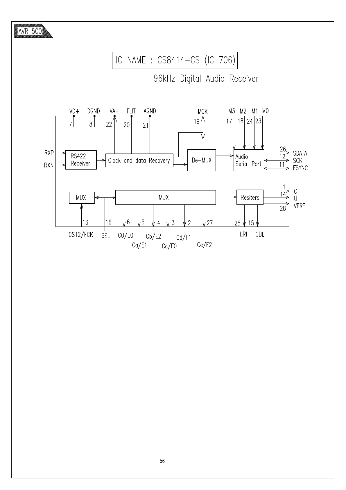
62
Page 63
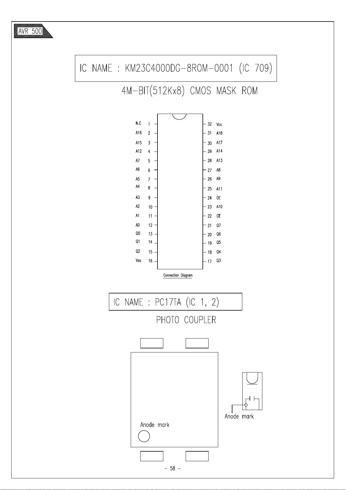
63
Page 64

64
Page 65

65
Page 66

66
Page 67

67
Page 68

68
Page 69

69
Page 70

70
Page 71

71
Page 72

72
Page 73

73
Page 74

74
Page 75

75
Page 76
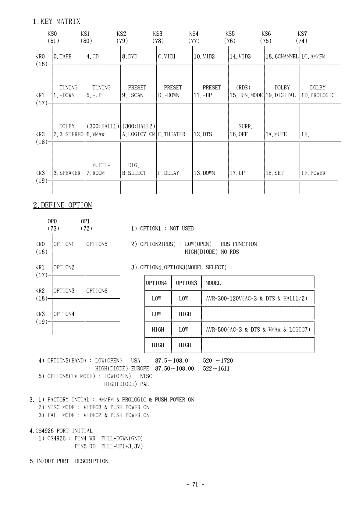
76
Page 77

77
Page 78

78
Page 79

79
Page 80

80
Page 81

81
Page 82

TYPE:
82
CM1684C
ANODE
&
GRID
ASIGNMENT
S1
S2
S3
S4
S5
S6
S7
S8
S9
S10
S11
S12
S13
S14
G1
THEA
TER
HALL
2
HALL
1
3-STEREO
PL
O
L
OGIC
DIGIT
AL
DISPLA
Y
NIGHT
MUL
TI
PCM
SLEEP
MUTE
BYPA
S
S
DSP
G2
o
d
e
m
n
i
c
g
RDS
k
p
q
a
b
G3
o
d
e
m
n
i
c
g
PTY
k
p
q
a
b
G4
o
d
e
m
n
i
c
g
CT
k
p
q
a
b
G5
o
d
e
m
n
i
c
g
RT
k
p
q
a
b
G6
o
d
e
m
n
i
c
g
TUNED
k
p
q
a
b
G7
o
d
e
m
n
i
c
g
k
p
q
a
b
G8
o
d
e
m
n
i
c
g
MONO
k
p
q
a
b
G9
o
d
e
m
n
i
c
g
STEREO
k
p
q
a
b
G10
o
d
e
m
n
i
c
g
k
p
q
a
b
G11
m
A
UTO
G12
o
d
e
n
i
c
g
k
p
q
a
b
o
d
e
m
n
i
c
g
MEMORY
k
p
q
a
b
G13
o
d
e
m
n
i
c
g
k
p
q
a
b
G14
MPEG
DTS
k1
d1
e1
c1
I1
J1
VMAX
g1
PRESET
a1
h1
i1
S15
S16
S17
S18
PIN
AS
SIGNMENT
Pin
Assignment
Pin
Assignment
F1,
F2
:
ALAL
OG
OPT
COAX
AC
-3
No.
No.
Filament
35
S2
G1
1
F1
G14
h
2
F1
36
S3
i
f
j
:
Grid
3
NP
37
S4
S1
h
i
f
j
4
NL
38
S5
S18
G1
39
S6
:
Anode
i
f
j
h
5
NL
6
G2
40
S7
i
f
j
h
7
G3
41
S8
:
NoLead
8
G4
42
G4
NP
i
f
j
h
G5
43
S10
:
N
o
9
Pin
i
f
j
h
10
G6
44
S11
11
G7
45
S12
i
f
j
h
12
G8
46
S13
i
f
j
h
13
G9
47
S14
14
G10
48
S15
i
f
j
h
15
G11
49
S16
i
f
j
h
16
G12
50
S17
17
G13
51
S18
i
f
j
h
18
G14
52
NL
i
f
j
h
19
33
NL
53
NP54F2
m1
f1
b1
n1
34
S1
55
F2
Page 83

83
Page 84

84
Page 85

85
Page 86

86
Page 87

87
Page 88

88
Page 89

89
Page 90

90
Page 91

91
Page 92

92
Page 93

93
Page 94

94
 Loading...