

Page 1
AVR 2650 harman/kardon
121
A3S56D30FTP
A3S56D40FTP
256M Double Data Rate Synchronous DRAM
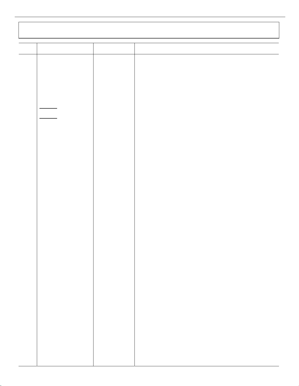
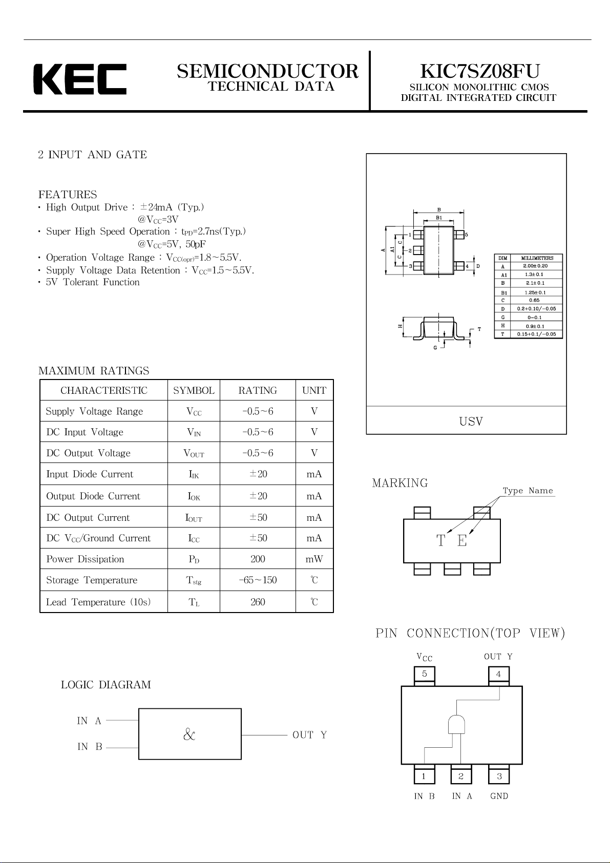
PIN FUNCTION
SYMBOL TYPE DESCRIPTION
Clock: CLK and /CLK are differential clock inputs. All address and control
CLK, /CLK Input
CKE
Input
input signals are sampled on the crossing of the positive edge of CLK and
negative edge of /CLK. Output (read) data is referenced to the crossings of
CLK and /CLK (both directions of crossing).
Clock Enable: CKE controls Power Down and Self Refresh.
Taking CKE LOW provides Precharge Power Down or Self Refresh (all banks idle),
or Active Power Down (row active in any bank).
Taking CKE HIGH provides Power Down exit or Self Refresh exit.
After Self Refresh is started, CKE becomes asynchronous input.
Power Down and Self Refresh is maintained as long as CKE is LOW.
/CS Input Chip Select: When /CS is HIGH, any command means No Operation.
/RAS, /CAS, /WE Input Combination of /RAS, /CAS, /WE defines basic commands.
A0-12 specify the Row / Column Address in conjunction with BA0,1. The
Row Address is specified by A0-12. The Column Address is specified by
A0-12 Input
BA0,1 Input
DQ0-7 (x8),
DQ0-15 (x16),
DQS (x8)
UDQS, LDQS (x16)
DM (x8)
UDM, LDM (x16)
Input / Output
Input / Output
Input
A0-9(x8) and A0-8(x16). A10 is also used to indicate precharge
option. When A10 is HIGH at a Read / Write command, an Auto Precharge
is performed. When A10 is HIGH at a Precharge command, all banks are precharged.
Bank Address: BA0,1 specifies one of four banks to which a command is applied.
BA0,1 must be set with Active, Precharge, Read, Write commands.
Data Input/Output: Data bus
Data Strobe: Output with read data, input with write data. Edge-aligned
with read data, centered in write data. Used to capture write data.
For the x16, LDQS corresponds to the data on DQ0-DQ7; UDQS
correspond to the data on DQ8-DQ15
Input Data Mask: DM is an input mask signal for write data. Input data
is masked when DM is sampled HIGH along with that input data
during a write access. DM is sampled on both edges of DQS.
Although DM pins are input only, the DM loading matches the DQ
and DQS loading. For the x16, LDM corresponds to the data on DQ0-DQ7;
UDM corresponds to the data on DQ8-DQ15.
Vdd, Vss Power Supply Power Supply for the memory array and peripheral circuitry.
VddQ, VssQ Power Supply VddQ and VssQ are supplied to DQ, DQS buffers.
VREF Input SSTL_2 reference voltage.
Page 2
AVR 2650 harman/kardon
122
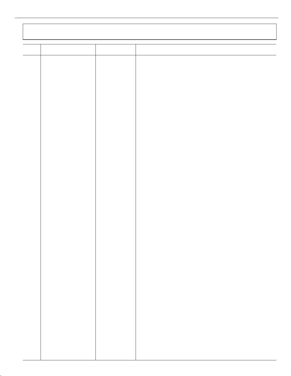
12-Bit, 170 MHz Video and Graphics Digitizer with
3D Comb Filter Decoder and
Quad HDMI 1.4 Fast Switching Receiver
PRELIMINARY
FEATURES
Quad HDMI 1.4 Fast Switching Receiver
170 MHz Video and Graphics Digitizer
3D Comb Filter Video Decoder
SCART Fast Blank Support
Adaptive HDMI Equaliser
Integrated CEC Controller
HDMI Repeater Support
Advanced VBI data slicer
Video and Graphics Digitizer
Four 170 MHz, 12-bit ADCs,
12-channel analog input mux
525i-/625i-component analog input
525p-/625p-component progressive scan support
720p-/1080i-/1080p-component HDTV support
Low refresh rates (24/25/30 Hz) support for 720p/1080p
Digitizes RGB graphics up to 1600 × 1200 at 60 Hz (UXGA)
3D Video Decoder
NTSC/PAL/SECAM color standards support
NTSC/PAL 2D/3D motion detecting comb filter
Advanced time-base correction (TBC) with frame
synchronization
Interlaced-to-progressive conversion for 525i and 625i
IF compensation filters
Vertical peaking and horizontal peaking filters
Robust synchronization extraction for poor video source
4:1 HDMI 1.4 225 MHz Receiver
Fast-Switching of HDMI ports
2:2 HEAC muxing support
2 HEAC channel support
2 Ethernet Interfaces for HEC Support
SPDIF interface for ARC support.
3D Video format support including frame packing 1080p
24Hz, 720p 50 Hz, 720p 60Hz
Full colorimetry support including sYCC601, Adobe RGB,
Adobe YCC 601
36-/30-bit Deep Color and 24-bit color support
HDCP 1.3 support with internal HDCP Keys
+5V Detect and Hot plug assert for each HDMI port
Full HDMI Audio Support including HBR, DSD, DST
Advanced Audio mute feature
Flexible digital audio output interfaces
ADV7844
Supports up to 5 SPDIF outputs,
Supports up to 4 I2S outputs
General
Highly flexible 36-bit pixel output interface
Internal EDID RAM for HDMI and graphics
Dual STDI (standard identification) function support
Any-to-any, 3 × 3 color space conversion (CSC) matrix
2 programmable interrupt request output pins
Simultaneous analog processing and HDMI monitoring
APPLICATIONS
Advanced TVs
PDP HDTVs
LCD TVs (HDTV ready)
LCD/DLP® rear projection HDTVs
CRT HDTVs
LCoS™ HDTVs
AVR video receivers
LCD/DLP front projectors
HDTV STBs with PVR
Projectors
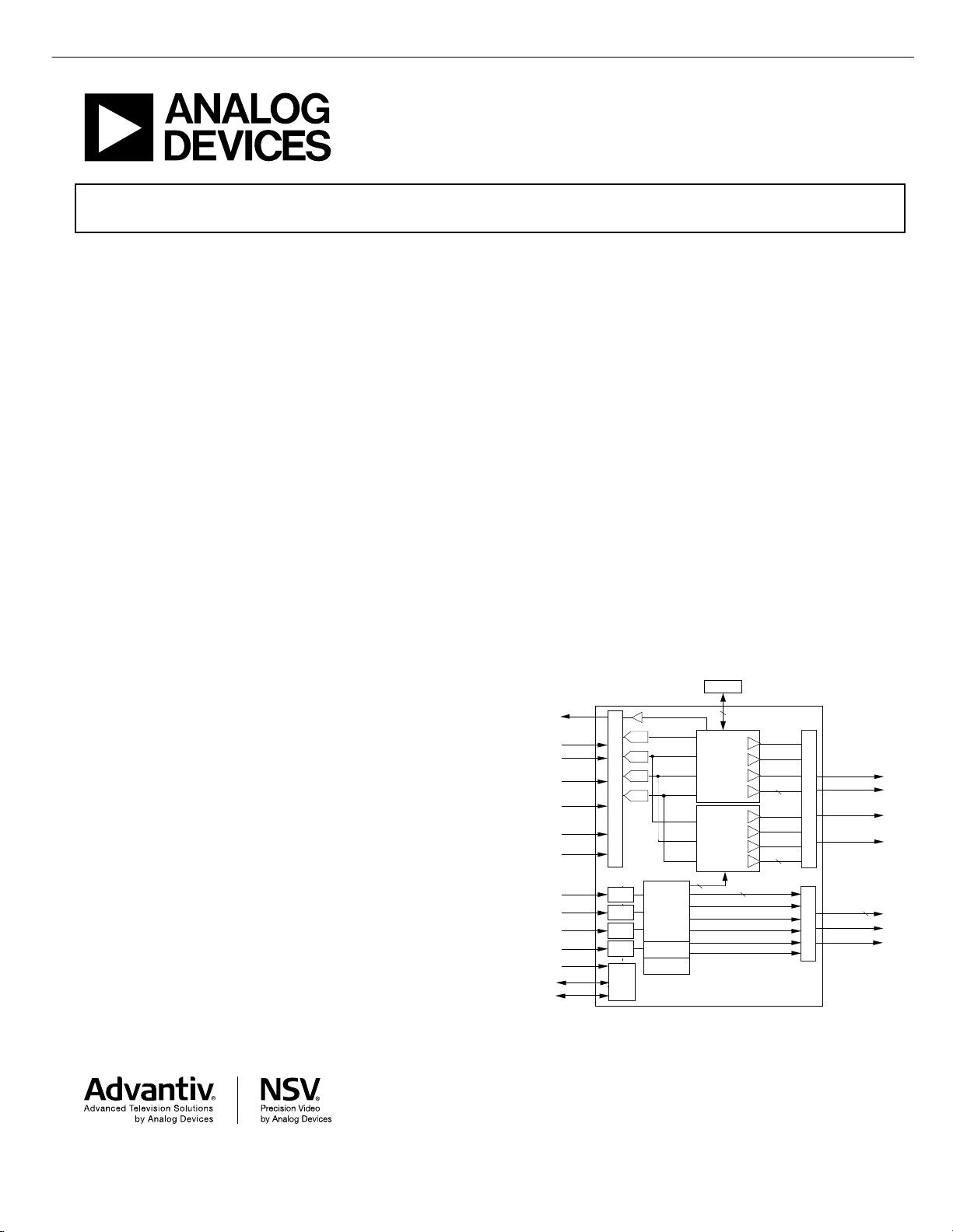
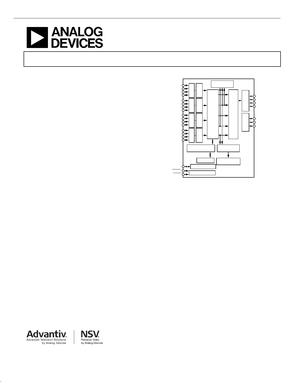
FUNCTIONAL BLOCK DIAGRAM
SDRAM
SCART
CVBS
SCART RGB
+CVBS
CVBS
SD/PS
YPbPr
HD YPbPr
GRAPHICS
RGB
HDMI 1
HDMI 2
HDMI 3
HDMI 4
SPDIF
ETHERNET 1
ETHERNET 2
YC
INPUT MUX
TMDS
DDC
TMDS
DDC
TMDS
DDC
TMDS
DDC
HEAC
ADC
ADC
ADC
ADC
SCART G
SCART B
SCART R
DEEP
COLOR
HDMI Rx
FAST
SWITCH
HDCP
KEYS
CVBS
CVBS
Y/G
Pb/B
Pr/R
Figure 1.
48
SDP
CVBS 3D YC
S-VIDEO
SCART
CP
YPbPr
525p/625p
720p/1080i
1080p/UXGA
RGB
36
4
HS/VS
FIELD/DE
CLK
DATA
HS/VS
FIELD/DE
CLK
DATA
I2S
SPDIF
DSD
HBR
MCLK
SCLK
ADV7844
HS/VS
FIELD/DE
CLK
OUTPUT MUX
36-BIT YCbCr
/RGB
AUDIO
OUTPUT
MCLK
SCLK
OUTPUT MUX
TO AUDIO
PROCESSOR
5
Page 3
AVR 2650 harman/kardon
123
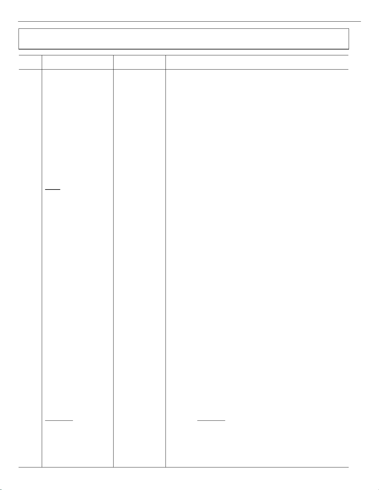
ADV7844 PRELIMINARY
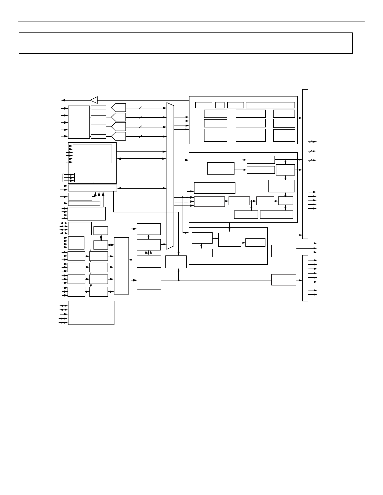
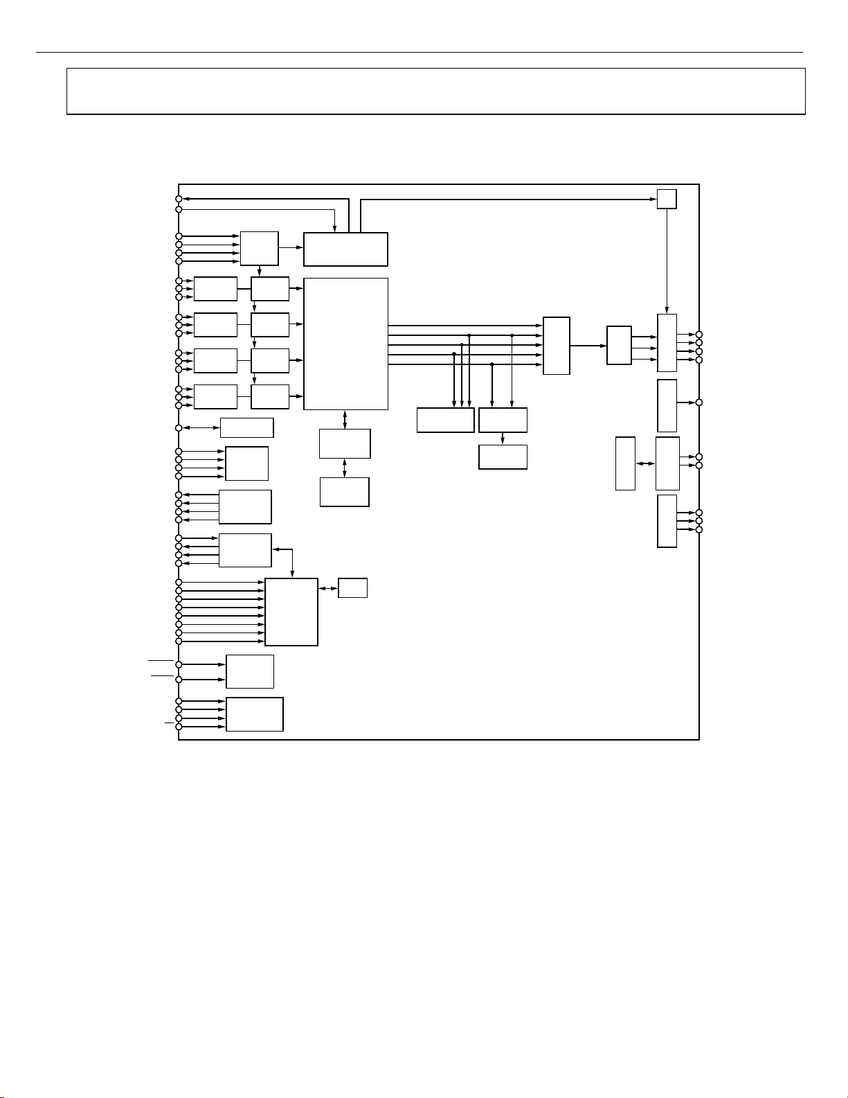
DETAILED FUNCTIONAL BLOCK DIAGRAM
AOUT
CVBS
SCART RGB
YPrPb
RGB
HS_IN1
VS_IN1
HS_IN2/TRI5
VS_IN2/TRI6
TRI1 TO
TRI4
SCL
SDA
AVLINK
CEC
RXA_5V / HPDA
RXB_5V / HPDB
RXC_5V / HPDC
RXD_5V / HPDD
DDCA_SDA / DDCA_SCL
DDCB_SDA / DDCB_SCL
DDCC_SDA / DDCC_SCL
DDCD_SDA / DDCD_SCL
RXA_C±
RXB_C±
RXC_C±
RXD_C±
RXA_0±
RXA_1±
RXA_2±
RXB_0±
RXB_1±
RXB_2±
RXC_0±
RXC_1±
RXC_2±
RXD_0±
RXD_1±
RXD_2±
HEAC_1±
HEAC_2±
SPDIF_IN
E1_TX±/E1_RX±
E2_TX±/E2_RX±
ANALOG FRONT END
YC
12-CHANNEL
INPUT
MATRIX
SYNC1
SYNC2
AND CLOCK GENERATION
2
C
AVLINK
CONTROLLER
CEC CONTROLLER
5V DETECT AND HPD
CONTROLLER
REPEATER
CONTROLLER
PLL
EQUALIZER SAMPLER
EQUALIZER SAMPLER
EQUALIZER SAMPLER
EQUALIZER SAMPLER
HDMI ETHERNET CHANNEL
AUDIO RETURN CHANNEL
CLAMP
CLAMP
CLAMP
CLAMP
LLC GENERATION
SYNC PROCESSING
TRI-LEVEL
SLICER
CONTROL INTERFACEI
EDID/
&
HDCP
EEPROM
HDCP
BLOCK
ADC0
ADC1
ADC2
ADC3
FASTSWITCHING
BLOCK + HDMI DECODE
12
12
12
12
HS/CS,VS/FIELD
CONTROL
AND DATA
DEEP COLOR
CONVERSION
4:2:2 TO 4:4:4
CONVERSION
+MUX
PROCESSOR
CONTROL
FILTER
PACKET
(A)
(B)
(C)
(D)
MUX
(A)
(B)
(C)
PACKET/
INFOFRAME
MEMORY
Figure 2. Detailed Functional Block Diagram
STANDARD DEFINITION PROCESSOR (SDP)
3D COMB
2D COMB
COMPONENT PROCESSOR
AND CGMS DETECTION
PROGRAMMABLE
DECODER
READBACK
TBC
VERTICAL
PEAKING
HORIZONTAL
PEAKING
CTI and LTI
DIGITAL PROCESSING BLOCK
SYNC SOURCE
AND POLARITY
DETECT
MACROVISION
DELAY
VSI
2
I
C
VIDEO DATA PROCESSOR
FINE CLAMP
ANCILLARY
DATA
FORMATTER
DIGITAL
CALIBRATION
DDR/SDR-SDRAM INTERFACE
STANDARD
AUTODECTION
MACROVISION
DETECTION
INTERLACE
TO PROGRESSIVE
CONVERSION
SYNC EXTRACT
(ESDP)
STANDARD
IDENTIFICATION
GAIN
CONTROL
FAST I
2
C
ACTIVE PEAK
AND HSYNC DEPTH
NOISE AND
INTERFACE
DECIMATION
FILTERS
COLOR SPACE
CONVERSION
FASTBLANK
OVERLAY
CONTROL
AV
CODE
INSERTION
CP CSC AND
DECIMATION
FILTERS
OFFSET
ADDER
INTERRUPT
CONTROLLER
AUDIO
PROCESSOR
12
P0 TO P11
12
P12 TO P23
12
P24 TO P35
VIDEO OUTPUT FORMATTER
LLC
HS/CS
VS/FIELD
DE
SYNC_OUT
TTX_SDA / TTX_SCL
INT1
INT2
AP0
AP1
AP2
AP3
AP4
AP5
SCLK
MCLK
AUDIO OUTPUT FORMATTER
Rev. PrC| Page 4 of 35
Page 4
AVR 2650 harman/kardon
124
ADV7844 PRELIMINARY
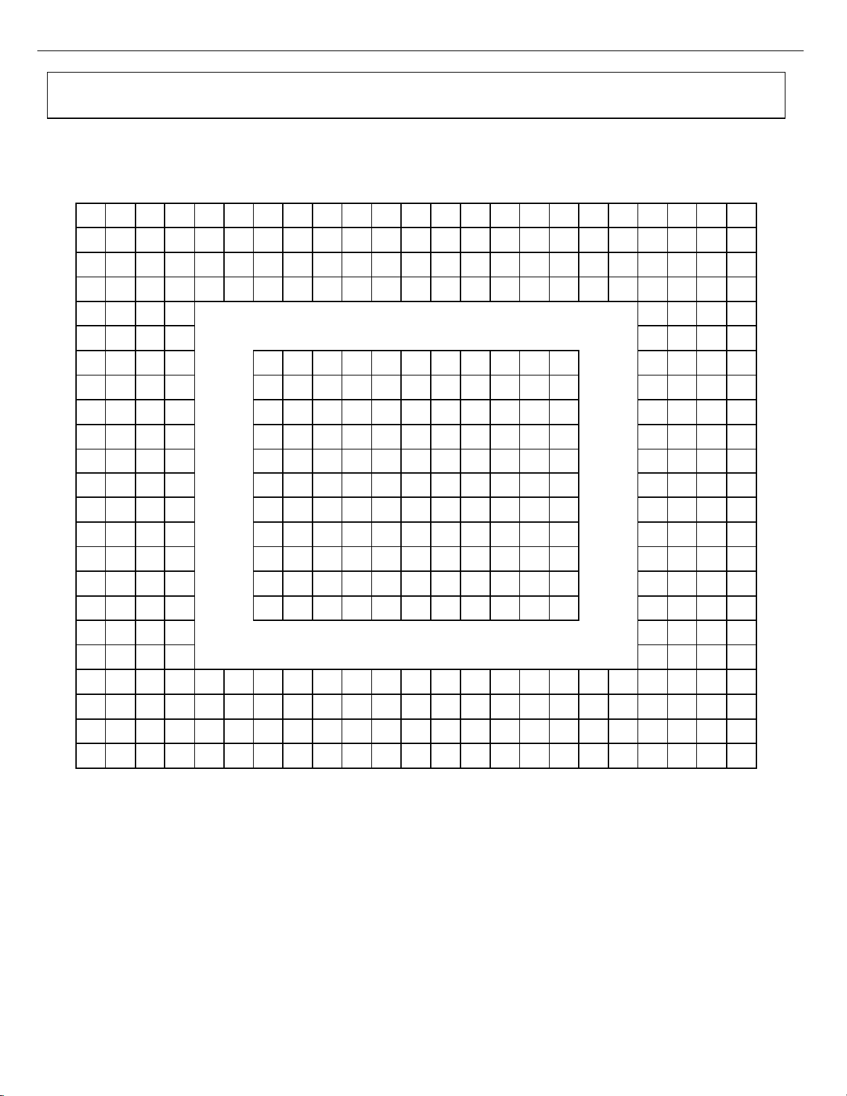
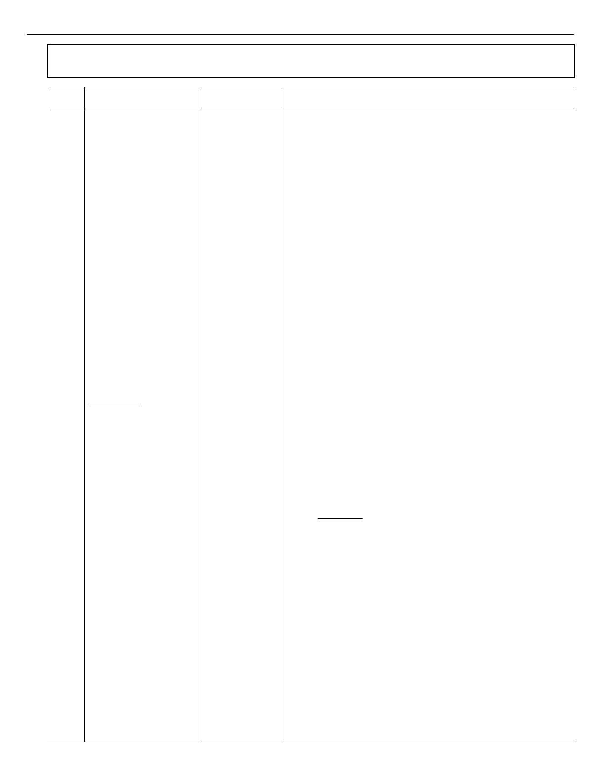
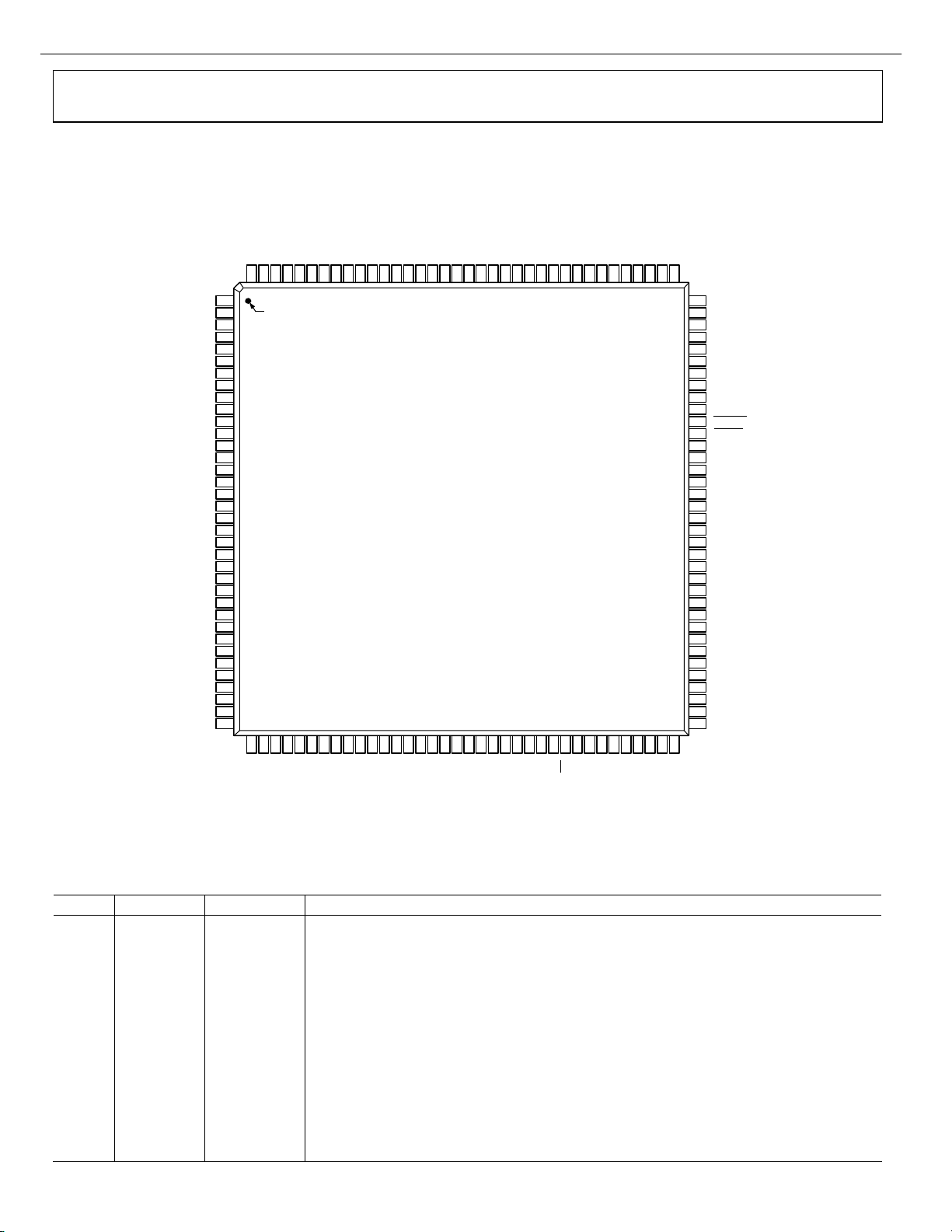
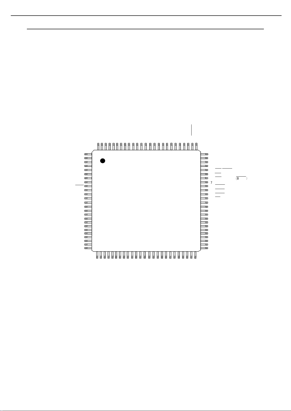
PIN CONFIGURATION AND FUNCTION DESCRIPTIONS
1 2 3 4 5 6 7 8 9 1011121314151617181920212223
GND VS/FIELD E2_TX+ E2_RX+ TVDD RXD_2- RXD_1- RXD_0- RXD_C- HEAC_2- TVDD RXC_2- RXC_1- RXC_0- RXC_C- TVDD RXB_2- RXB_1- RXB_0- RXB_C- HEAC_1- GND
A
HS/CS FIELD/DE E2_TX- E2_RX- TVDD RXD_2+ RXD_1+ RXD_0+ RXD_C+ HEAC_2+ TVDD RXC_2+ RXC_1+ RXC_0+ RXC_C+ TVDD RXB_2+ RXB_1+ RXB_0+ RXB_C+ HEAC_1+ GND
B
P0 P1 E1_TX+ E1_RX+ TVDD PWRDN1 PWRDN2 HPA_D RXD_5V RXC_5V TVDD GND GND GND GND GND GND TVDD TVDD TVDD TVDD TVDD TVDD
C
P2 P3 E1_TX- E1_RX- TVDD
D
DVDDIO DVDDIO GND GND
E
P5 P4 EP_MISO EP_MOSI
F
SYNC_OUT
CEC HPA_C RXB_5V HPA_B TVDD RXA_5V HPA_A
DDCD_SDA DDCD_SCL DDCC_SDA DDCC _SCL
NC
NC
DDCB_SDA DDCB_SCL
RTERM
DDCA_SDA
DDCA_SCL
TVDD RXA_2+ RXA_2-
CVDD RXA_1+ RXA_1-
CVDD RXA_0+ RXA_0-
G
H
DDVCADS_AGVCVDDCVDDCVDDDNGDNGDNGDNGDNGDNGDNGDNGLCS_XTTADS_XTT8P9P
J
K
L
M
N
P
HS_IN2/TRI7
R
DNGDNGDNGDNGDNGDNGDNGDNGDNGDNGDDV1TNI4TSET12P02P
VS_IN2/TRI8
T
U
NC NC
SYNC4 AIN10
A
B
C
D
E
F
-C_AXR+C_AXRDDVCLCS_AGVCVDDCVDDCVDDDNGDNG2TSET1TSETDNGDNGDNGDNGKCS_PESC_PE6P7P
G
H
DNGDNG3TSETDDVPDNGDNGDNGDNGDNGDNGDNGDNGDNGDNGDNG0PAKLCM01P11P
J
PLATXNLATXDNGDDVPDNGDNGDNGDNGDNGDNGDNGDNGDNGDNGDDVKLCS5PA21P31P
K
DNGDNGDNGDNGDNGDNGDNGDNGDNGDNGDNGDNGDNGDNGDDVDNGDNGOIDDVDOIDDVD
L
PFERNFERDNGDNGDNGDNGDNGDNGDNGDNGDNGDNGDNGDNGDDV3PA4PA41P51P
M
DDVADDVADDVADDVADNGDNGDNGDNGDNGDNGDNGDNGDNGDNGDDV1PA2PA61P71P
N
21NIA11NIADDVADDVADNGDNGDNGDNGDNGDNGDNGDNGDNGDNGDDVADSLCS91P81P
P
R
DNGDNGDNGDNGDNGDNGDNGDNGDNGDNGDNGDNGDNGDNGDDV2TNI5TSET32P22P
T
8NIA9NIA3IRT4IRTDNGDNGDNGDDVDDVDDVDDVDDVDDVDDVDDVOIDDVDOIDDVDOIDDVDOIDDVD
U
LLC P24 RESET AVLINK TRI1 TRI2 SYNC3 AIN7
V
P25 P26 SPDIF_IN AVDD AVDD AVDD AVDD
W
P27 P28 GND GND GND
Y
P29 P30 GND GND GND
AA
P31 P32 P34 GND DVDDIO
AB
GND P33 P35 GND DVDDIO
AC
NC
VDD_SDRAM
SDRAM_A11 SDRA M_A6 SDRAM _A2 SDRAM_CS
VDD_SDRAM
SDRAM_A9 SDRAM _A5 SDRAM _A1
NC
NC
SDRAM_A8 SDRAM _A4 SDRAM _A0
SDRAM_A7 SDRAM _A3 SDRAM_A10
SDRAM_LDQS
SDRAM_RAS SDRA M_ DQ 7
SDRAM_CAS VDD_SDRAM SDRAM_DQ4 SDRAM_DQ0 SDRAM_DQ13 SDRAM_DQ9 SDRAM_CKN VDD_SDRAM
SDRAM_BA1
SDRAM_BA0
SDRAM_WE
SDRAM_DQ6 SDRAM_DQ2 SDRAM_DQ15 SDRAM_DQ11 SDRAM_CKE VDD_SDRAM
GND
SDRAM_DQ5 SDRAM_DQ1 SDRAM_DQ12 SDRAM_DQ8
GND
VDD_ SDR AM SDR AM_D Q3 SDRAM_VREF SDRAM_DQ14 SDRAM_DQ10
SDRAM_CK
SDRAM_UDQS
GND AOUT NC AIN5 AIN6
VDD_SDRAM
GND NC NC SYNC2 AIN4
GND SYNC1
VDD_SDRAM
GNDAIN1AIN2AIN3GND
HS_IN1/TRI5
1 2 3 4 5 6 7 8 9 1011121314151617181920212223
Figure 7. Pin Configuration
VS_IN1/TRI6
GND
V
W
Y
AA
AB
AC
Rev. PrBC | Page 12 of 35
Page 5

AVR 2650 harman/kardon
125
PRELIMINARY ADV7844
Table 6. Function Descriptions
Pin
No.
A1 GND Ground Ground
A2 VS/FIELD Digital video
A3 E2_TX+ Digital output Digital Output Channel 2 True of Ethernet Interface
A4 E2_RX+ Digital input Digital Input Channel 2 True of Ethernet Interface
A5 TVDD Power Terminator Supply Voltage (3.3 V).
A6 RXD_2- HDMI input Digital Input Channel 2 Complement of Port D in the HDMI Interface.
A7 RXD_1- HDMI input Digital Input Channel 1 Complement of Port D in the HDMI Interface.
A8 RXD_0- HDMI input Digital Input Channel 0 Complement of Port D in the HDMI Interface.
A9 RXD_C- HDMI input Digital Input Clock Complement of Port D in the HDMI Interface.
A10 HEAC_2- HDMI input/output HDMI Ethernet and Audio Return Channel (HEAC) Complement Channel 2 in
A11 TVDD Power Terminator Supply Voltage (3.3 V).
A12 RXC_2- HDMI input Digital Input Channel 2 Complement of Port C in the HDMI Interface.
A13 RXC_1- HDMI input Digital Input Channel 1 Complement of Port C in the HDMI Interface.
A14 RXC_0- HDMI input Digital Input Channel 0 Complement of Port C in the HDMI Interface.
A15 RXC_C- HDMI input Digital Input Clock Complement of Port C in the HDMI Interface.
A16 NC No connect No Connect.
A17 TVDD Power Terminator Supply Voltage (3.3 V).
A18 RXB_2- HDMI input Digital Input Channel 2 Complement of Port B in the HDMI Interface.
A19 RXB_1- HDMI input Digital Input Channel 1 Complement of Port B in the HDMI Interface.
A20 RXB_0- HDMI input Digital Input Channel 0 Complement of Port B in the HDMI Interface.
A21 RXB_C- HDMI input Digital Input Clock Complement of Port B in the HDMI Interface.
A22 HEAC_1- HDMI input/output HDMI Ethernet and Audio Return Channel (HEAC) Complement Channel 1 in
A23 GND Ground Ground
B1 HS/CS Digital video
B2 FIELD/DE Miscellaneous
B3 E2_TX- Digital output Digital Output Channel 2 Complimentary of Ethernet Interface
B4 E2_RX- Digital input Digital Input Channel 2 Complimentary of Ethernet Interface
B5 TVDD Power Terminator Supply Voltage (3.3 V).
B6 RXD_2+ HDMI input Digital Input Channel 2 True of Port D in the HDMI Interface.
B7 RXD_1+ HDMI input Digital Input Channel 1 True of Port D in the HDMI Interface.
B8 RXD_0+ HDMI input Digital Input Channel 0 True of Port D in the HDMI Interface.
B9 RXD_C+ HDMI input Digital Input Clock True of Port D in the HDMI Interface.
B10 HEAC_2+ HDMI input/output HDMI Ethernet and Audio Return Channel (HEAC) True Channel 2 in HDMI
B11 TVDD Power Terminator Supply Voltage (3.3 V).
B12 RXC_2+ HDMI input Digital Input Channel 2 True Of Port C in the HDMI Interface.
B13 RXC_1+ HDMI input Digital Input Channel 1 True Of Port C in the HDMI Interface.
B14 RXC_0+ HDMI input Digital Input Channel 0 True Of Port C in the HDMI Interface.
B15 RXC_C+ HDMI input Digital Input Clock True Of Port C in the HDMI Interface.
B16 NC No Connect No Connect.
B17 TVDD Power Terminator Supply Voltage (3.3 V).
B18 RXB_2+ HDMI input Digital Input Channel 2 True of Port B in the HDMI Interface.
B19 RXB_1+ HDMI input Digital Input Channel 1 True of Port B in the HDMI Interface.
B20 RXB_0+ HDMI input Digital Input Channel 0 True of Port B in the HDMI Interface.
B21 RXB_C+ HDMI input Digital Input Clock True of Port B in the HDMI Interface.
Mnemonic Type Description
VS is a vertical synchronization output signal. FIELD is a field
output
output
digital
synchronization output signal in all interlaced video modes. VS or FIELD can
be configured for this pin.
HDMI Interface
HDMI Interface
HS is a horizontal synchronization output signal. CS (composite
synchronization) signal is a single signal containing both horizontal and
vertical synchronization pulses.
DE (data enable) is a signal that indicates active pixel data. FIELD is a field
synchronization output signal in all interlaced video modes. DE or FIELD can
be configured for this pin.
Interface
Rev. PrC| Page 13 of 35
Page 6
AVR 2650 harman/kardon
126
ADV7844 PRELIMINARY
Pin
No. Mnemonic Type Description
B22 HEAC_1+ HDMI input/output HDMI Ethernet and Audio Return Channel (HEAC ) True Channel 1 in HDMI
Interface
B23 GND Ground Ground
C1 P0 Digital video
output
C2 P1 Digital video
output
C3 E1_TX+ Digital output Digital Output Channel 1 True of Ethernet Interface
C4 E1_RX+ Digital input Digital Input Channel 1 True of Ethernet Interface
C5 TVDD Power Terminator Supply Voltage (3.3 V).
C6
C7
C8 HPA_D Miscellaneous
C9 RXD_5V HDMI input 5 V Detect Pin for Port D in the HDMI Interface.
C10 RXC_5V HDMI input 5 V Detect Pin for Port C in the HDMI Interface.
C11 TVDD Power Terminator Supply Voltage (3.3 V).
C12 GND Ground Ground
C13 GND Ground Ground
C14 GND Ground Ground
C15 GND Ground Ground
C16 GND Ground Ground
C17 GND Ground Ground
C18 TVDD Power Terminator Supply Voltage (3.3 V).
C19 TVDD Power Terminator Supply Voltage (3.3 V).
C20 TVDD Power Terminator Supply Voltage (3.3 V).
C21 TVDD Power Terminator Supply Voltage (3.3 V).
C22 TVDD Power Terminator Supply Voltage (3.3 V).
C23 TVDD Power Terminator Supply Voltage (3.3 V).
D1 P2 Digital video
D2 P3 Digital video
D3 E1_TX- Digital output Digital Output Channel 1 Complimentary of Ethernet Interface
D4 E1_RX- Digital input Digital Input Channel 1 Complimentary of Ethernet Interface
D5 TVDD Power Terminator Supply Voltage (3.3 V).
D6 SYNC_OUT Miscellaneous
D7 CEC Digital
D8 HPA_C Miscellaneous
D9 RXB_5V HDMI input 5 V Detect Pin for Port B in the HDMI Interface.
D10 HPA_B Miscellaneous
D11 TVDD Power Terminator Supply Voltage (3.3 V).
D12 RXA_5V HDMI input 5 V Detect Pin for Port A in the HDMI Interface.
D13 HPA_A Miscellaneous
D14 DDCD_SDA HDMI input HDCP Slave Serial Data Port D. DDCD_SDA is a 3.3 V input that is 5 V tolerant.
D15 DDCD_SCL HDMI input HDCP Slave Serial Clock Port D. DDCD_SCL is a 3.3 V input that is 5 V
D16 DDCC_SDA HDMI input HDCP Slave Serial Data Port C. DDCC_SDA is a 3.3 V input that is 5 V tolerant.
D17 DDCC_SCL HDMI input HDCP Slave Serial Clock Port C. DDCC_SCL is a 3.3 V input that is 5 V tolerant.
D18 RTERM Miscellaneous Sets Internal Termination Resistance. A 500 Ω resistor between this pin and
PWRDN1
PWRDN2
Miscellaneous
digital
Test pin This pin should be connected to the ground.
digital
output
output
digital
input/output
digital
digital
digital
Video Pixel Output Port.
Video Pixel Output Port.
Controls the Power-Up of the ADV7844. Should be connected to a digital 3.3
V I/O supply to power up the ADV7844.
Hot Plug Assert signal output for HDMI port D.
Video Pixel Output Port.
Video Pixel Output Port.
Sliced synchronization output.
Consumer Electronic Control Channel.
Hot Plug Assert signal output for HDMI port C.
Hot Plug Assert signal output for HDMI port B.
Hot Plug Assert signal output for HDMI port A.
tolerant.
Rev. PrBC | Page 14 of 35
Page 7

AVR 2650 harman/kardon
127
PRELIMINARY ADV7844
Pin
No. Mnemonic Type Description
analog GND should be used.
D19 DDCB_SDA HDMI input HDCP Slave Serial Data Port B. DDCB_SDA is a 3.3 V input that is 5 V tolerant.
D20 DDCB_SCL HDMI input HDCP Slave Serial Clock Port B. DDCB_SCL is a 3.3 V input that is 5 V tolerant.
D21 TVDD Power Terminator Supply Voltage (3.3 V).
D22 RXA_2+ HDMI input Digital Input Channel 2 True of Port A in the HDMI Interface.
D23 RXA_2- HDMI input Digital Input Channel 2 Complement of Port A in the HDMI Interface.
E1 DVDDIO Power Digital I/O Supply Voltage (3.3 V).
E2 DVDDIO Power Digital I/O Supply Voltage (3.3 V).
E3 GND Ground Ground
E4 GND Ground Ground
E20 DDCA_SDA HDMI input HDCP Slave Serial Data Port A. DDCA_SDA is a 3.3 V input that is 5 V tolerant.
E21 CVDD Power Comparator Supply Voltage (1.8 V).
E22 RXA_1+ HDMI input Digital Input Channel 1 True of Port A in the HDMI Interface.
E23 RXA_1- HDMI input Digital Input Channel 1 Complement of Port A in the HDMI Interface.
F1 P5 Digital video
output
F2 P4 Digital video
output
F3 EP_MISO Digital output SPI Master In/Slave Out for External EDID Interface.
F4 EP_MOSI Digital input SPI Master Out/Slave In for External EDID Interface.
F20 DDCA_SCL HDMI input HDCP Slave Serial Clock Port A. DDCA_SCL is a 3.3 V input that is 5 V
F21 CVDD Power Comparator Supply Voltage (1.8 V).
F22 RXA_0+ HDMI input Digital Input Channel 0 True of Port A in the HDMI Interface.
F23 RXA_0- HDMI input Digital Input Channel 0 Complement of Port A in the HDMI Interface.
G1 P7 Digital video
output
G2 P6 Digital video
output
G3
G4 EP_SCK Digital output SPI Clock for External EDID Interface.
G7 GND Ground Ground
G8 GND Ground Ground
G9 GND Ground Ground
G10 GND Ground Ground
G11 TEST1 Test Do Not Connect.
G12 TEST2 Test Do Not Connect.
G13 GND Ground Ground
G14 GND Ground Ground
G15 CVDD Power Comparator Supply Voltage (1.8 V).
G16 CVDD Power Comparator Supply Voltage (1.8 V).
G17 CVDD Power Comparator Supply Voltage (1.8 V).
G20 VGA_SCL Miscellaneous
G21 CVDD Power Comparator Supply Voltage (1.8 V).
G22 RXA_C+ HDMI input Digital Input Clock True of Port A in the HDMI Interface.
G23 RXA_C- HDMI input Digital Input Clock Complement of Port A in the HDMI Interface.
H1 P9 Digital video
H2 P8 Digital video
H3 TTX_SDA Miscellaneous
H4 TTX_SCL Miscellaneous
EP_CS
Digital output SPI Chip Select for External EDID Interface.
digital
output
output
digital
digital
Video Pixel Output Port.
Video Pixel Output Port.
tolerant.
Video Pixel Output Port.
Video Pixel Output Port.
DDC Port Serial Clock Input for VGA
Video Pixel Output Port.
Video Pixel Output Port.
I2C Port Serial Data Input/Output Pin. SDA is the data line for the teletext
port.
I2C Port Serial Clock Input. SCL is the clock line for the teletext port.
Rev. PrC| Page 15 of 35
Page 8

AVR 2650 harman/kardon
128
ADV7844 PRELIMINARY
Pin
No. Mnemonic Type Description
H7 GND Ground Ground
H8 GND Ground Ground
H9 GND Ground Ground
H10 GND Ground Ground
H11 GND Ground Ground
H12 GND Ground Ground
H13 GND Ground Ground
H14 GND Ground Ground
H15 CVDD Power Comparator Supply Voltage (1.8 V).
H16 CVDD Power Comparator Supply Voltage (1.8 V).
H17 CVDD Power Comparator Supply Voltage (1.8 V).
H20 VGA_SDA Miscellaneous
digital
H21 CVDD Power Comparator Supply Voltage (1.8 V).
H22 NC No Connect No Connect
H23 NC No Connect No Connect
J1 P11 Digital video
output
J2 P10 Digital video
output
J3 MCLK Miscellaneous Audio Master Clock Output.
J4 AP0 Miscellaneous Audio Output Pin. Pins AP0-AP5 can be configured to output SPDIF Digital
J7 GND Ground Ground
J8 GND Ground Ground
J9 GND Ground Ground
J10 GND Ground Ground
J11 GND Ground Ground
J12 GND Ground Ground
J13 GND Ground Ground
J14 GND Ground Ground
J15 GND Ground Ground
J16 GND Ground Ground
J17 GND Ground Ground
J20 PVDD Power PLL Supply Voltage (1.8 V).
J21 TEST3 Test Do Not Connect.
J22 GND Ground Ground
J23 GND Ground Ground
K1 P13 Digital video
output
K2 P12 Digital video
output
K3 AP5 Miscellaneous Audio Output Pin. Pins AP0-AP5 can be configured to output SPDIF Digital
K4 SCLK Miscellaneous
digital
K7 VDD Power Digital Core Supply Voltage (1.8 V).
K8 GND Ground Ground
K9 GND Ground Ground
K10 GND Ground Ground
K11 GND Ground Ground
K12 GND Ground Ground
DDC Port Data Clock Input for VGA
Video Pixel Output Port.
Video Pixel Output Port.
Audio Output (SPDIF), High Bit Rate (HBR), Direct Stream Digital (DSD),
Direct Stream Transfer (DST) or I2S.
Video Pixel Output Port.
Video Pixel Output Port.
Audio Output (SPDIF), High Bit Rate (HBR), Direct Stream Digital (DSD),
Direct Stream Transfer (DST) or I2S.
Audio Serial Clock Output.
Rev. PrBC | Page 16 of 35
Page 9
AVR 2650 harman/kardon
129
PRELIMINARY ADV7844
Pin
No. Mnemonic Type Description
K13 GND Ground Ground
K14 GND Ground Ground
K15 GND Ground Ground
K16 GND Ground Ground
K17 GND Ground Ground
K20 PVDD Power PLL Supply Voltage (1.8 V).
K21 GND Ground Ground
K22 XTALN Miscellaneous
analog
K23 XTALP Miscellaneous
analog
L1 DVDDIO Power Digital I/O Supply Voltage (3.3 V).
L2 DVDDIO Power Digital I/O Supply Voltage (3.3 V).
L3 GND Ground Ground
L4 GND Ground Ground
L7 VDD Power Digital Core Supply Voltage (1.8 V).
L8 GND Ground Ground
L9 GND Ground Ground
L10 GND Ground Ground
L11 GND Ground Ground
L12 GND Ground Ground
L13 GND Ground Ground
L14 GND Ground Ground
L15 GND Ground Ground
L16 GND Ground Ground
L17 GND Ground Ground
L20 GND Ground Ground
L21 GND Ground Ground
L22 GND Ground Ground
L23 GND Ground Ground
M1 P15 Digital video
output
M2 P14 Digital video
output
M3 AP4 Miscellaneous Audio Output Pin. Pins AP0-AP5 can be configured to output SPDIF Digital
M4 AP3 Miscellaneous Audio Output Pin. Pins AP0-AP5 can be configured to output SPDIF Digital
M7 VDD Power Digital Core Supply Voltage (1.8 V).
M8 GND Ground Ground
M9 GND Ground Ground
M10 GND Ground Ground
M11 GND Ground Ground
M12 GND Ground Ground
M13 GND Ground Ground
M14 GND Ground Ground
M15 GND Ground Ground
M16 GND Ground Ground
M17 GND Ground Ground
M20 GND Ground Ground
M21 GND Ground Ground
M22 REFN Miscellaneous Internal Voltage Reference Output.
Input Pin for 28.63636 MHz Crystal.
Crystal Input. Input pin for 28.63636 MHz Crystal or an External 1.8 V,
28.63636 MHz Clock Oscillator Source to Clock the ADV7844.
Video Pixel Output Port.
Video Pixel Output Port.
Audio Output (SPDIF), High Bit Rate (HBR), Direct Stream Digital (DSD),
Direct Stream Transfer (DST) or I2S.
Audio Output (SPDIF), High Bit Rate (HBR), Direct Stream Digital (DSD),
Direct Stream Transfer (DST) or I2S.
Rev. PrC| Page 17 of 35
Page 10

AVR 2650 harman/kardon
130
ADV7844 PRELIMINARY
Pin
No.
M23 REFP Miscellaneous
N1 P17 Digital video
N2 P16 Digital video
N3 AP2 Miscellaneous Audio Output Pin. Pins AP0-AP5 can be configured to output SPDIF Digital
N4 AP1 Miscellaneous Audio Output Pin. Pins AP0-AP5 can be configured to output SPDIF Digital
N7 VDD Power Digital Core Supply Voltage (1.8 V).
N8 GND Ground Ground
N9 GND Ground Ground
N10 GND Ground Ground
N11 GND Ground Ground
N12 GND Ground Ground
N13 GND Ground Ground
N14 GND Ground Ground
N15 GND Ground Ground
N16 GND Ground Ground
N17 GND Ground Ground
N20 AVDD Power Analog Supply Voltage (1.8 V).
N21 AVDD Power Analog Supply Voltage (1.8 V).
N22 AVDD Power Analog Supply Voltage (1.8 V).
N23 AVDD Power Analog Supply Voltage (1.8 V).
P1 P18 Digital video
P2 P19 Digital video
P3 SCL Miscellaneous
P4 SDA Miscellaneous
P7 VDD Power Digital Core Supply Voltage (1.8 V).
P8 GND Ground Ground
P9 GND Ground Ground
P10 GND Ground Ground
P11 GND Ground Ground
P12 GND Ground Ground
P13 GND Ground Ground
P14 GND Ground Ground
P15 GND Ground Ground
P16 GND Ground Ground
P17 GND Ground Ground
P20 AVDD Power Analog Supply Voltage (1.8 V).
P21 AVDD Power Analog Supply Voltage (1.8 V).
P22 AIN11 Analog video input Analog Video Input Channel.
P23 AIN12 Analog video input Analog Video Input Channel.
R1 P20 Digital video
R2 P21 Digital video
R3 TEST4 Test Do Not Connect.
Mnemonic Type Description
analog
Internal Voltage Reference Output.
analog
Video Pixel Output Port.
output
Video Pixel Output Port.
output
Audio Output (SPDIF), High Bit Rate (HBR), Direct Stream Digital (DSD),
Direct Stream Transfer (DST) or I2S.
Audio Output (SPDIF), High Bit Rate (HBR), Direct Stream Digital (DSD),
Direct Stream Transfer (DST) or I2S.
Video Pixel Output Port.
output
Video Pixel Output Port.
output
I2C Port Serial Clock Input. SCL is the clock line for the control port.
digital
I2C Port Serial Data Input/Output Pin. SDA is the data line for the control
digital
output
output
port.
Video Pixel Output Port.
Video Pixel Output Port.
Rev. PrBC | Page 18 of 35
Page 11

AVR 2650 harman/kardon
131
PRELIMINARY ADV7844
Pin
No. Mnemonic Type Description
R4 INT1 Miscellaneous
digital
R7 VDD Power Digital Core Supply Voltage (1.8 V).
R8 GND Ground Ground
R9 GND Ground Ground
R10 GND Ground Ground
R11 GND Ground Ground
R12 GND Ground Ground
R13 GND Ground Ground
R14 GND Ground Ground
R15 GND Ground Ground
R16 GND Ground Ground
R17 GND Ground Ground
R20 HS_IN2/TRI7 Miscellaneous
analog
R21 VS_IN2/TRI8 Miscellaneous
analog
R22 SYNC4 Miscellaneous
analog
R23 AIN10 Analog video input Analog Video Input Channel.
T1 P22 Digital video
output
T2 P23 Digital video
output
T3 TEST5 Test Do Not Connect.
T4 INT2 Miscellaneous
digital
T7 VDD Power Digital Core Supply Voltage (1.8 V).
T8 GND Ground Ground
T9 GND Ground Ground
T10 GND Ground Ground
T11 GND Ground Ground
T12 GND Ground Ground
T13 GND Ground Ground
T14 GND Ground Ground
T15 GND Ground Ground
T16 GND Ground Ground
T17 GND Ground Ground
T20 GND Ground Ground
T21 GND Ground Ground
T22 GND Ground Ground
T23 GND Ground Ground
U1 DVDDIO Power Digital I/O Supply Voltage (3.3 V).
U2 DVDDIO Power Digital I/O Supply Voltage (3.3 V).
U3 DVDDIO Power Digital I/O Supply Voltage (3.3 V).
U4 DVDDIO Power Digital I/O Supply Voltage (3.3 V).
U7 VDD Power Digital Core Supply Voltage (1.8 V).
U8 VDD Power Digital Core Supply Voltage (1.8 V).
U9 VDD Power Digital Core Supply Voltage (1.8 V).
U10 VDD Power Digital Core Supply Voltage (1.8 V).
Interrupt. This pin can be active low or active high. When status bits change,
this pin is triggered. The events that trigger an interrupt are under user
control.
HS on Graphics Port 2. The HS input signal is used for 5-wire timing mode.
This pin can also be used as a trilevel/bilevel input on the SCART or Dterminal connector. Result available via I2C.
VS on Graphics Port 2. The VS input signal is used for 5-wire timing mode.
This pin can also be used as a trilevel/bilevel input on the SCART or Dterminal connector. Result available via I
This is a synchronization on green or luma input (SOG/SOY) used in
embedded synchronization mode. User configurable.
Video Pixel Output Port.
Video Pixel Output Port.
Interrupt. This pin can be active low or active high. When status bits change,
this pin is triggered. The events that trigger an interrupt are under user
control.
2
C.
Rev. PrC| Page 19 of 35
Page 12
AVR 2650 harman/kardon
132
ADV7844 PRELIMINARY
Pin
No.
U11 VDD Power Digital Core Supply Voltage (1.8 V).
U12 VDD Power Digital Core Supply Voltage (1.8 V).
U13 VDD Power Digital Core Supply Voltage (1.8 V).
U14 VDD Power Digital Core Supply Voltage (1.8 V).
U15 GND Ground Ground
U16 GND Ground Ground
U17 GND Ground Ground
U20 TRI4 Miscellaneous
U21 TRI3 Miscellaneous
U22 AIN9 Analog video input Analog Video Input Channel.
U23 AIN8 Analog video input Analog Video Input Channel.
V1 LLC Digital video
V2 P24 Digital video
V3
V4 AVLINK Digital
V20 TRI1 Miscellaneous
V21 TRI2 Miscellaneous
V22 SYNC3 Miscellaneous
V23 AIN7 Analog video input Analog Video Input Channel.
W1 P25 Digital video
W2 P26 Digital video
W3 NC No connect No Connect.
W4 SPDIF_IN Miscellaneous
W20 AVDD Power Analog Supply Voltage (1.8 V).
W21 AVDD Power Analog Supply Voltage (1.8 V).
W22 AVDD Power Analog Supply Voltage (1.8 V).
W23 AVDD Power Analog Supply Voltage (1.8 V).
Y1 P27 Digital video
Y2 P28 Digital video
Y3 GND Ground Ground
Y4 GND Ground Ground
Y5 GND Ground Ground
Y6 VDD_SDRAM Power External Memory Interface Digital Input/Output Supply (DDR 2.5 V or SDR
Y7 SDRAM_A11 SDRAM interface Address Output. Interface to external RAM address lines.
Y8 SDRAM_A6 SDRAM interface Address Output. Interface to external RAM address lines.
Y9 SDRAM_A2 SDRAM interface Address Output. Interface to external RAM address lines.
Y10
Y11 SDRAM_LDQS SDRAM interface Lower Data Strobe Pin. Data strobe pins are used for the RAM interface. This
Y12 GND Ground Ground
Mnemonic Type Description
Trilevel/Bilevel Input on the SCART or D-Terminal Connector. Result available
RESET
SDRAM_CS
analog
analog
output
output
Miscellaneous
digital
input/output
analog
analog
analog
output
output
digital
output
output
SDRAM interface
via I2C.
Trilevel/Bilevel Input on the SCART or D-Terminal Connector. Result available
via I2C.
Line-Locked Output Clock for the Pixel Data (Range is 13.5 MHz to 170 MHz).
Video Pixel Output Port.
System Reset Input. Active low. A minimum low reset pulse width of 5 ms is
required to reset the ADV7844 circuitry.
Digital SCART Control Channel.
Trilevel/Bilevel Input on the SCART or D-Terminal Connector. Result available
via I2C.
Trilevel/Bilevel Input on the SCART or D-Terminal Connector. Result available
via I2C.
This is a synchronization on green or luma input (SOG/SOY) used in
embedded synchronization mode. User configurable.
Video Pixel Output Port.
Video Pixel Output Port.
Audio Clock Input Pin for SPDIF
Video Pixel Output Port.
Video Pixel Output Port.
3.3 V).
Chip Select.
RAM. One of four command signals to the external SDRAM.
is an output with read data and an input with write data. It is edge aligned
with write data and centered in read data. SDRAM_ LDQS corresponds to
the data on SDRAM_DQ0 to SDRAM_
Rev. PrBC | Page 20 of 35
SDRAM_CS
enables and disables the command decoder on the
Page 13
AVR 2650 harman/kardon
133
PRELIMINARY ADV7844
Pin
No.
Y13 SDRAM_DQ6 SDRAM interface Data Bus. Interface to external RAM 16-bit data bus.
Y14 SDRAM_DQ2 SDRAM interface Data Bus. Interface to external RAM 16-bit data bus.
Y15 SDRAM_DQ15 SDRAM interface Data Bus. Interface to external RAM 16-bit data bus.
Y16 SDRAM_DQ11 SDRAM interface Data Bus. Interface to external RAM 16-bit data bus.
Y17 SDRAM_CKE SDRAM interface Clock Enable. This pin acts as an enable to the clock signals of the external
Y18 VDD_SDRAM Power External Memory Interface Digital Input/Output Supply (DDR 2.5 V or SDR
Y19 GND Ground Ground
Y20 AOUT Analog monitor
Y21 NC No connect No Connect.
Y22 AIN5 Analog video input Analog Video Input Channel.
Y23 AIN6 Analog video input Analog Video Input Channel.
AA1 P29 Digital video
AA2 P30 Digital video
AA3 GND Ground Ground
AA4 GND Ground Ground
AA5 GND Ground Ground
AA6 VDD_SDRAM Power External Memory Interface Digital Input/Output Supply (DDR 2.5 V or SDR
AA7 SDRAM_A9 SDRAM interface Address Output. Interface to external RAM address lines.
AA8 SDRAM_A5 SDRAM interface Address Output. Interface to external RAM address lines.
AA9 SDRAM_A1 SDRAM interface Address Output. Interface to external RAM address lines.
AA10
AA11 SDRAM_DQ7 SDRAM interface Data Bus. Interface to external RAM 16-bit data bus.
AA12 GND Ground Ground
AA13 SDRAM_DQ5 SDRAM interface Data Bus. Interface to external RAM 16-bit data bus.
AA14 SDRAM_DQ1 SDRAM interface Data Bus. Interface to external RAM 16-bit data bus.
AA15 SDRAM_DQ12 SDRAM interface Data Bus. Interface to external RAM 16-bit data bus.
AA16 SDRAM_DQ8 SDRAM interface Data Bus. Interface to external RAM 16-bit data bus.
AA17 SDRAM_CK SDRAM interface Differential Clock Output. All address and control output signals to the RAM
AA18 VDD_SDRAM Power External Memory Interface Digital Input/Output Supply (DDR 2.5 V or SDR
AA19 GND Ground Ground
AA20 NC No connect No Connect.
AA21 NC No connect No Connect.
AA22 SYNC2 Miscellaneous
AA23 AIN4 Analog video input Analog Video Input Channel.
AB1 P31 Digital video
AB2 P32 Digital video
AB3 P34 Digital video
AB4 NC No connect No Connect.
AB5 GND Ground Ground
AB6 DVDDIO Power Digital I/O Supply Voltage (3.3 V).
AB7 SDRAM_A8 SDRAM interface Address Output. Interface to external RAM address lines.
AB8 SDRAM_A4 SDRAM interface Address Output. Interface to external RAM address lines.
Mnemonic Type Description
RAM.
3.3 V).
Analog Monitor Output.
output
Video Pixel Output Port.
output
Video Pixel Output Port.
output
3.3 V).
SDRAM_RAS
SDRAM interface Row Address Select Command Signal. One of four command signals to the
external SDRAM.
should be sampled on the positive edge of SDRAM_CK and on the negative
analog
output
output
output
edge of
3.3 V).
This is a synchronization on green or luma input (SOG/SOY) used in
embedded synchronization mode. User configurable.
Video Pixel Output Port.
Video Pixel Output Port.
Video Pixel Output Port.
SDRAM_CK
.
Rev. PrC| Page 21 of 35
Page 14
AVR 2650 harman/kardon
134
ADV7844 PRELIMINARY
Pin
No.
AB9 SDRAM_A0 SDRAM interface Address Output. Interface to external RAM address lines.
AB10 SDRAM_BA1 SDRAM interface Bank Address Output. Interface to external RAM bank address lines.
AB11
AB12 VDD_SDRAM Power External Memory Interface Digital Input/Output Supply (DDR 2.5 V or SDR
AB13 SDRAM_DQ4 SDRAM interface Data Bus. Interface to external RAM 16-bit data bus.
AB14 SDRAM_DQ0 SDRAM interface Data Bus. Interface to external RAM 16-bit data bus.
AB15 SDRAM_DQ13 SDRAM interface Data Bus. Interface to external RAM 16-bit data bus.
AB16 SDRAM_DQ9 SDRAM interface Data Bus. Interface to external RAM 16-bit data bus.
AB17
AB18 VDD_SDRAM Power External Memory Interface Digital Input/Output Supply (DDR 2.5 V or SDR
AB19 GND Ground Ground
AB20 SYNC1 Miscellaneous
AB21 HS_IN1/TRI5 Miscellaneous
AB22 VS_IN1/TRI6 Miscellaneous
AB23 GND Ground Ground
AC1 GND Ground Ground
AC2 P33 Digital video
AC3 P35 Digital video
AC4 NC No connect No Connect.
AC5 GND Ground Ground
AC6 DVDDIO Power Digital I/O Supply Voltage (3.3 V).
AC7 SDRAM_A7 SDRAM interface Address Output. Interface to external RAM address lines.
AC8 SDRAM_A3 SDRAM interface Address Output. Interface to external RAM address lines.
AC9 SDRAM_A10 SDRAM interface Address Output. Interface to external RAM address lines.
AC10 SDRAM_BA0 SDRAM interface Bank Address Output. Interface to external RAM bank address lines.
AC11
AC12 VDD_SDRAM Power External Memory Interface Digital Input/Output Supply (DDR 2.5 V or SDR
AC13 SDRAM_DQ3 SDRAM interface Data Bus. Interface to external RAM 16-bit data bus.
AC14 SDRAM_VREF SDRAM interface 1.25 V Reference for DDR SDRAM Interface or 1.65 V for SDR.
AC15 SDRAM_DQ14 SDRAM interface Data Bus. Interface to external RAM 16-bit data bus.
AC16 SDRAM_DQ10 SDRAM interface Data Bus. Interface to external RAM 16-bit data bus.
AC17 SDRAM_UDQS SDRAM interface Upper Data Strobe Pin. Data strobe pins for the RAM interface. This is an
AC18 VDD_SDRAM Power External Memory Interface Digital Input/Output Supply (DDR 2.5 V or SDR
AC19 GND Ground Ground
AC20 AIN1 Analog video input Analog Video Input Channel.
AC21 AIN2 Analog video input Analog Video Input Channel.
AC22 AIN3 Analog video input Analog Video Input Channel.
AC23 GND Ground Ground
Mnemonic Type Description
SDRAM_CAS
SDRAM_CK
SDRAM_WE
SDRAM interface Column Address Select Command Signal. One of four command signals to
the external SDRAM.
3.3 V).
SDRAM interface Differential Clock Output. All address and control output signals to the RAM
should be sampled on the positive edge of SDRAM_CK and on the negative
edge of
3.3 V).
This is a synchronization on green or luma input (SOG/SOY) used in
analog
analog
analog
output
output
SDRAM interface Write Enable Output Command Signal. One of four command signals to the
embedded synchronization mode. User configurable.
HS on Graphics Port 1. The HS input signal is used for 5-wire timing mode.
HS_IN1/TRI5 is a 3.3 V input that is 5 V tolerant.
Vertical Synchronization Input Signal. Used for 5-wire timing mode.
Video Pixel Output Port.
Video Pixel Output Port.
external SDRAM.
3.3 V).
output with read data and an input with write data. It is edge aligned with
write data and centered in read data. UDQS corresponds to the data on DQ8
to DQ16.
3.3 V).
SDRAM_CK
.
Rev. PrBC | Page 22 of 35
Page 15
AVR 2650 harman/kardon
135
HDMI 1.4 Mux with
ADI Confidential
FEATURES
4-input, 1-output HDMI mux
HDMI 1.4a support: 3D TV formats, content type bits,
CEC 1.4-compatible
Xpressview fast switching on all HDMI input ports
High-bandwidth digital content protection (HDCP 1.4a)
HDCP repeater support
225 MHz HDMI Rx and Tx support 36-/30-/24-bit Deep Color
Ultralow jitter digital PLL (100% deskew)
Quad HDMI Rx input
Adaptive equalizer for cable lengths up to 30 meters
Internal extended display identification data (EDID) RAM
EDID replication (512 bytes per port)
EDID with HDMI cable 5 V power support
5 V detect inputs
Hot plug assertion control pins
Single HDMI Tx output: EDID data extraction and hot plug
detect (HPD) input
HDMI 1.4a audio pass-through support
2
I
S, DSD, and HBR, including Dolby TrueHD and
DTS-HD master audio
General
Interrupt controller with 3 interrupt outputs
Software libraries, driver, and application available
2-layer PCB design supported
144-lead, 20 mm × 20 mm LQFP package
APPLICATIONS
Port expansion for Analog Devices HDMI decoders
Audio video receivers (AVRs)
Home theater in a box (HTiB)
Sound bar with HDMI repeater support
Flat panel TVs
Other repeater applications
GENERAL DESCRIPTION
The ADV3014 is a high performance, four-input, one-output,
High-Definition Multimedia Interface (HDMI™) switch that
integrates HDMI 1.4a receiver and transmitter functions onto
one chip. It supports all HDCP repeater functions through fully
tested Analog Devices, Inc., repeater software libraries and drivers.
The ADV3014 incorporates Xpressview™ fast switching on all
Xpressview Fast Switching
ADV3014
FUNCTIONAL BLOCK DIAGRAM
SYNC
AND DDC
AND DDC
AND DDC
AND DDC
MEASUREMENT
PROCESSOR
Xpressview™ FAST
SWITCHING RECEIVER
PACKET
PROCESSOR
INFOFRAME/
PACKET MEMORY
Figure 1.
HDCP
ENGINE
ENCRYPTION
ADV3014
RX0±
RX1±
RX2±
AND TMDS
RXC±
HDMI ENCODER
INT1
INT2
INT_TX
INTERRUPT
CONTROLLER
09068-001
RXA_0±
RXA_1±
RXA_2±
RXA_C±
RXB_0±
RXB_1±
RXB_2±
RXB_C±
RXC_0±
RXC_1±
RXC_2±
RXC_C±
RXD_0±
RXD_1±
RXD_2±
RXD_C±
PWRDN
RESET
CEC
EQ
TMDS
EQ
TMDS
EQ
TMDS
EQ
TMDS
HDCP
DECRYPTION ENGI NE
HDCP KEYS
CEC CONTRO L L ER
GLOBAL CONTROLS
input HDMI ports. Using the Analog Devices hardware-based
HDCP engine that minimizes software overhead, Xpressview
technology allows fast switching between any HDMI input
ports in less than 1 second.
The ADV3014 supports all mandatory HDMI 1.4a 3D TV formats
in addition to all HD TV formats up to 1080p 36-bit Deep Color.
The ADV3014 also features an integrated HDMI 1.4 CEC controller, which supports capability discovery and control (CDC).
The HDMI receiver supports programmable/adaptive equalization that ensures robust operation of the interface at cable lengths
of up to 30 meters.
The ADV3014 offers integrated control of hot plug circuits,
sensing of 5 V input signals and on-board EDID controls with
EDID replication and power-down mode EDID.
The ADV3014 supports pass-through of all HDMI 1.4a audio
formats including I
2
S, DSD, and HBR formats such as Dolby®
TrueHD and DTS-HD® master audio.
Fabricated in an advanced CMOS process, the ADV3014 is
provided in a space-saving, 144-lead, 20 mm × 20 mm LQFP
surface-mount, Pb-free package. It is specified over the 0°C to
70°C temperature range.
Page 16
AVR 2650 harman/kardon
136
ADI Confidential ADV3014
DETAILED FUNCTIONAL BLOCK DIAGRAM
XTAL
XTAL1
RXA_C+/RXA_C–
RXB_C+/RXB_C–
RXC_C+/RXC_C–
RXD_C+/RXD_C–
RXA_0+/RXA_0–
RXA_1+/RXA_1–
RXA_2+/RXA_2–
RXB_0+/RXB_0–
RXB_1+/RXB_1–
RXB_2+/RXB_2–
RXC_0+/RXC_0–
RXC_1+/RXC_1–
RXC_2+/RXC_2–
RXD_0+/RXD_0–
RXD_1+/RXD_1–
RXD_2+/RXD_2–
CEC
5V_DETA
5V_DETB
5V_DETC
5V_DETD
HP_CTRLA
HP_CTRLB
HP_CTRLC
HP_CTRLD
EP_MISO
EP_MOSI
EP_CS
EP_SCK
DDCA_SDA
DDCA_SCL
DDCB_SDA
DDCB_SCL
DDCC_SDA
DDCC_SCL
DDCD_SDA
DDCD_SCL
EQUALIZER
EQUALIZER
EQUALIZER
EQUALIZER
CONTROLLER
CONTROLLER
SPI MASTER/
RX
PLL
SAMPLER
SAMPLER
SAMPLER
SAMPLER
CEC
5V DETECT
RX HPD
SLAVE
RX EDID/
REPEATER
CONTROLLER
VIDEO/AUDIO
CLOCK
GENERATION
XPRESSVIEW™
FAST SWITCHING
RECEIVER
PROCESSOR
+
BACKGROUND
MEASUREMENT
HDCP
DECRYPTION
ENGINE
HDCP KEYS
EDID
RAM
VIDEO DATA
DE
VS
HS
AUDIO DATA
MEASUREMENT
SYNC
PACKET
PROCESSOR
INFOFRAME
PACKET
MEMORY
HDCP
ENCRYPTION
TX
PLL
CH0
CH1
HDMI
ENGINE
CH2
ENCODER
BUFFER
EDID/HDCP
TXC+/TXC–
TX0+/TX0–
TX1+/TX1–
TX2+/TX2–
SERIALIZER
TMDS DRIV ERS
HP_TX
TX HPD
CONTROLLER
TXDDC_SDA
TXDDC_SCL
TX
EDID/HDCP
CONTROLLER
INT1
INT2
INT_TX
INTERRUPT
CONTROLLER
PWRDN
RESET
SCL
SDATA
ALSB
CS
GLOBAL
CONTROLS
2
I
C
CONTROLLER
ADV3014
09068-001
Figure 2. Detailed Functional Block Diagram
Rev. Sp0 | Page 3 of 16
Page 17
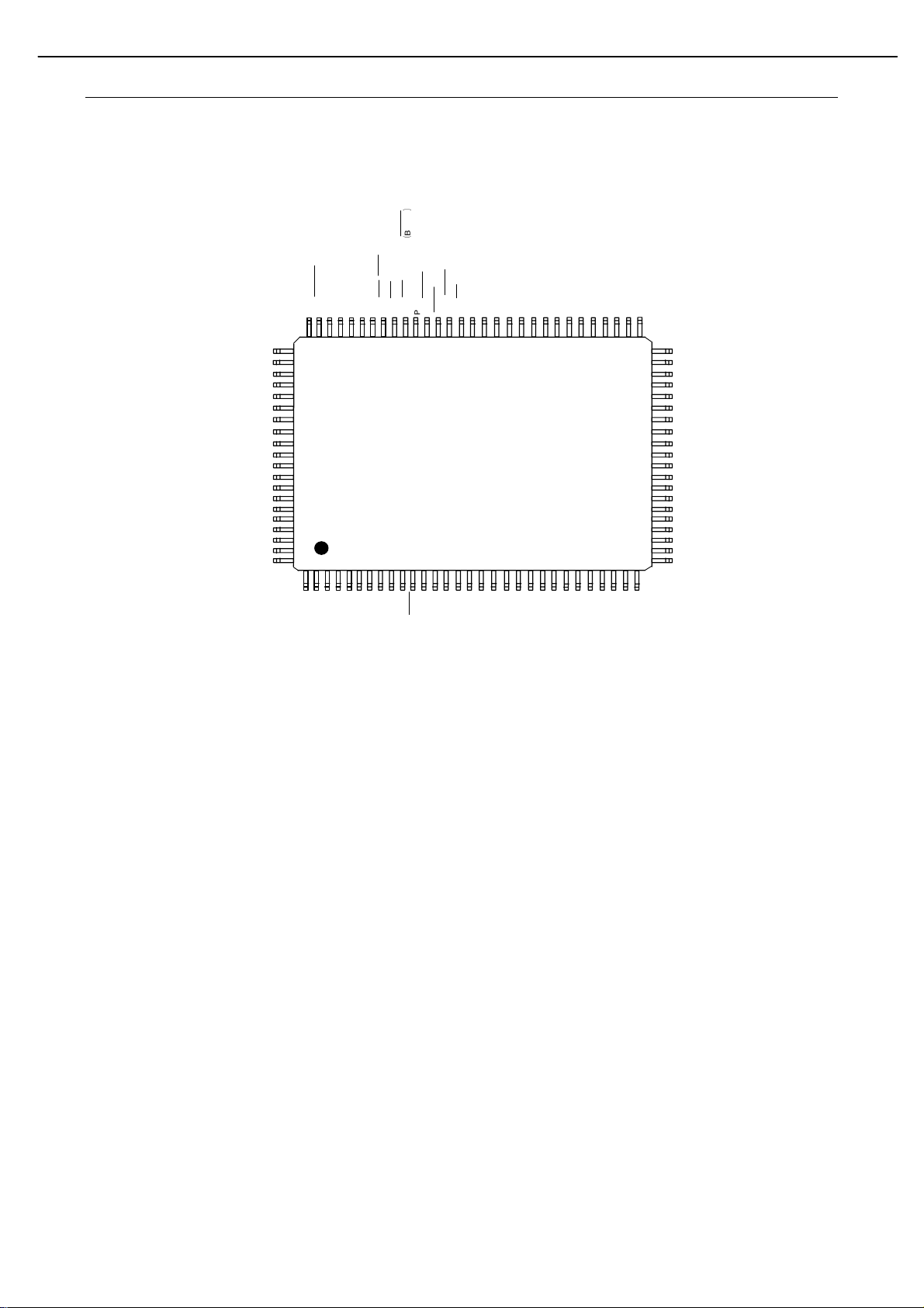
A
A
AVR 2650 harman/kardon
137
ADV3014 ADI Confidential
PIN CONFIGURATION AND FUNCTION DESCRIPTIONS
5V_DETC
HP_CTRLC
RXB_2+
RXB_2–
TVDD
RXB_1+
RXB_1–
CGND
RXB_0+
RXB_0–
TVDD
RXB_C+
RXB_C–
CGND
CVDD
DDCB_SCL
DDCB_SDA
DVDD
DGND
5V_DETB
HP_CTRLB
RXA_2+
RXA_2–
TVDD
RXA_1+
RXA_1–
CGND
RXA_0+
RXA_0–
TVDD
RXA_C+
RXA_C–
CGND
CVDD
DDCC_SDA
113
114
115
116
117
118
119
120
121
122
123
124
125
126
127
128
129
130
131
132
133
134
135
136
137
138
139
140
141
142
143
144
CVDD
CGND
TVDD
CGND
TVDD
DGND
DVDD
CVDD
CGND
TVDD
CGND
TVDD
CVDD
CGND
1
PIN 1
2
3
4
5
6
7
8
9
10
11
12
13
14
15
16
17
18
19
20
21
22
23
24
25
26
27
28
29
30
31
32
33
34
35
36
37
38
39
404142434445464748495051525354555657585960616263646566676869707172
TXC–
TXAVDD
TXC+
TXGND
TEST0
HP_TX
TXPGND
TXPLVDD
TXPLGND
XDDC_SD
EXT_SWING
TXDDC_SCL
TX0–
TXGND
ADV3014
TOP VIEW
(Not to S cale)
TX1–
TX0+
TX1+
TXGND
TXAVDD
DGND
DVDD
CS
ALSB
EP_SCK
TEST1
EP_CS
EP_MOSI
EP_MISO
CEC
TX2–
TX2+
TXGND
DDCC_SCL
RXC_C–
RXC_C+
RXC_0–
RXC_0+
RXC_1–
RXC_1+
RXC_2–
RXC_2+
HP_CTRLD
5V_DETD
DDCD_SD
DDCD_SCL
RXD_C–
RXD_C+
RXD_0–
RXD_0+
RXD_1–
RXD_1+
RXD_2–
RXD_2+
TXPVDD
Figure 4. Pin Configuration
DDCA_SCL
109
110
111
112
108
DDCA_SDA
107
RTERM
106
5V_DETA
105
HP_CTRLA
104
PGND
103
PVDD
102
XTAL1
101
XTAL
100
PVDD
99
PGND
98
PWRDN
97
RESET
96
TEST16
95
TEST15
94
TEST14
93
DVDD
92
DGND
91
TEST13
90
TEST12
89
TEST11
88
TEST10
87
TEST9
86
DVDDIO
85
DGNDIO
84
INT_TX
83
INT2
82
INT1
81
DVDD
80
DGND
79
SCL
78
SDATA
77
TEST8
76
TEST7
75
TEST6
74
TEST5
73
DVDDIO
TEST2
TEST3
TEST4
DGNDIO
9068-002
Table 5: Pin Function Descriptions
Pin No. Mnemonic Type Description
1 DDCC_SCL Digital input HDCP Slave Serial Clock Port C. DDCC_SCL is a 3.3 V input that is 5 V tolerant.
2 CVDD Power Receiver Comparator Supply Voltage (1.8 V).
3 CGND Ground TVDD and CVDD Ground.
4 RXC_C− HDMI input Digital Input Clock Complement of Port C in the HDMI Interface.
5 RXC_C+ HDMI input Digital Input Clock True of Port C in the HDMI Interface.
6 TVDD Power Receiver Terminator Supply Voltage (3.3 V).
7 RXC_0− HDMI input Digital Input Channel 0 Complement of Port C in the HDMI Interface.
8 RXC_0+ HDMI input Digital Input Channel 0 True of Port C in the HDMI Interface.
9 CGND Ground TVDD and CVDD Ground.
10 RXC_1− HDMI input Digital Input Channel 1 Complement of Port C in the HDMI Interface.
11 RXC_1+ HDMI input Digital Input Channel 1 True of Port C in the HDMI Interface.
12 TVDD Power Receiver Terminator Supply Voltage (3.3 V).
13 RXC_2− HDMI input Digital Input Channel 2 Complement of Port C in the HDMI Interface.
Rev. Sp0 | Page 8 of 16
Page 18

AVR 2650 harman/kardon
138
ADI Confidential ADV3014
Pin No. Mnemonic Type Description
14 RXC_2+ HDMI input Digital Input Channel 2 True of Port C in the HDMI Interface.
15 HP_CTRLD Digital output Hot Plug Control Output for Port D. This pin is 5 V tolerant.
16 5V_DETD HDMI input 5 V Detect Pin for Port D in the HDMI Interface. This pin is 5 V tolerant.
17 DGND Ground DVDD Ground.
18 DVDD Power Digital Supply Voltage (1.8 V).
19 DDCD_SDA Digital I/O HDCP Slave Serial Data Port D. DDCD_SDA is a 3.3 V input that is 5 V tolerant.
20 DDCD_SCL Digital Input HDCP Slave Serial Clock Port D. DDCD_SCL is a 3.3 V input that is 5 V tolerant.
21 CVDD Power Comparator Supply Voltage (1.8 V).
22 CGND Ground TVDD and CVDD Ground.
23 RXD_C− HDMI input Digital Input Clock Complement of Port D in the HDMI Interface.
24 RXD_C+ HDMI input Digital Input Clock True of Port D in the HDMI Interface.
25 TVDD Power Terminator Supply Voltage (3.3 V).
26 RXD_0- HDMI input Digital Input Channel 0 Complement of Port D in the HDMI Interface.
27 RXD_0+ HDMI input Digital Input Channel 0 True of Port D in the HDMI Interface.
28 CGND Ground TVDD and CVDD Ground.
29 RXD_1− HDMI input Digital Input Channel 1 Complement of Port D in the HDMI Interface.
30 RXD_1+ HDMI input Digital Input Channel 1 True of Port D in the HDMI Interface.
31 TVDD Power Terminator Supply Voltage (3.3 V).
32 RXD_2− HDMI input Digital Input Channel 2 Complement of Port D in the HDMI Interface.
33 RXD_2+ HDMI input Digital Input Channel 2 True of Port D in the HDMI Interface.
34 CVDD Power Comparator Supply Voltage (1.8 V).
35 CGND Ground TVDD and CVDD Ground.
36 TXPVDD Power
37 TXPLVDD Power 1.8 V power supply
38 TXPGND Ground TXPVDD Ground.
39 TXPLGND Ground TXPLVDD Ground
40 EXT_SWING Analog input
41 HP_TX Analog input
42 TEST0 Test pin Connect to ground.
43 TXDDC_SDA Digital I/O
44 TXDDC_SCL Digital output
45 TXAVDD Power 1.8 V Power Supply for TMDS Outputs.
46 TXGND Ground TXAVDD Ground.
47 TXC− HDMI output
48 TXC+ HDMI output
49 TXGND Ground TXAVDD Ground.
50 TX0− HDMI output
51 TX0+ HDMI output
52 TXGND Ground TXAVDD Ground.
53 TX1− HDMI output
54 TX1+ HDMI output
55 TXAVDD Power 1.8 V Power Supply for TMDS Outputs.
56 TX2− HDMI output
1.8 V PLL Power Supply. These pins provide power to the digital portion of the clock PLL. The
designer should provide quiet, noise-free power to these pins.
Sets Internal Reference Currents. Place an 887Ω resistor (1% tolerance) between this pin and
ground.
Hot Plug Detect Signal. This pin indicates to the interface whether the receiver is connected.
This pin is 5 V tolerant.
Serial Port Data I/O to Receiver. This pin serves as the master to the DDC bus. This pin is 5 V
tolerant.
Serial Port Data Clock to Receiver. This pin serves as the master clock for the DDC bus.
This pin is 5 V tolerant.
Differential Clock Output. Differential clock output at the TMDS clock rate; supports
TMDS logic level.
Differential Clock Output. Differential clock output at the TMDS clock rate; supports
TMDS logic level.
Differential Output Channel 0 Complement. Differential output of the red data at 10×
the pixel clock rate; supports TMDS logic level.
Differential Output Channel 0 True. Differential output of the red data at 10× the pixel clock
rate; supports TMDS logic level.
Differential Output Channel 1 Complement. Differential output of the red data at 10×
the pixel clock rate; supports TMDS logic level.
Differential Output Channel 1 True. Differential output of the red data at 10× the pixel
clock rate; supports TMDS logic level.
Differential Output Channel 2 Complement. Differential output of the red data at 10×
the pixel clock rate; supports TMDS logic level.
Rev. Sp0 | Page 9 of 16
Page 19
AVR 2650 harman/kardon
139
ADV3014 ADI Confidential
Pin No. Mnemonic Type Description
57 TX2+ HDMI output
58 TXGND Ground TXAVDD Ground.
59 CEC Digital I/O Consumer Electronics Control Channel. This pin is 5 V tolerant.
60 DGND Ground DVDD Ground.
61 DVDD Power Digital Supply Voltage (1.8 V).
62 ALSB Digital input This pin is used to set the I2C address of the Rx IO and the Tx main maps.
Digital input
Digital input
Digital input
Miscellaneous
analog
63
64 EP_SCK Digital output SPI Clock Interface for the EDID.
65 EP_CS Digital output SPI Chip Selected Interface for the EDID.
66 EP_MOSI Digital output SPI Master Out/Slave In for the EDID.
67 EP_MISO Digital input SPI Master In/Slave Out for the EDID.
68 TEST1 Test pin Connect to ground.
69 TEST2 Test pin Connect to ground.
70 TEST3 Test pin Connect to ground.
71 TEST4 Test pin Connect to ground.
72 DGNDIO Ground DVDDIO Ground.
73 DVDDIO Power Digital I/O Supply Voltage (3.3 V).
74 TEST5 Test pin Connect to ground.
75 TEST6 Test pin Connect to ground.
76 TEST7 Test pin Connect to ground.
77 TEST8 Test pin Connect to ground.
78 SDATA Digital I/O I2C Port Serial Data Input/Output Pin. SDATA is the data line for the control port.
79 SCL Digital input I2C Port Serial Clock Input. SCL is the clock line for the control port.
80 DGND Ground DVDD Ground.
81 DVDD Power Digital Supply Voltage (1.8 V).
82 INT1 Digital output
83 INT2 Digital output
84 INT_TX Digital output Interrupt; Open Drain. A 2 kΩ pull-up resistor to the microcontroller I/O supply is recommended.
85 DGNDIO Ground DVDDIO Ground.
86 DVDDIO Power Digital I/O Supply Voltage (3.3 V).
87 TEST9 Test pin Leave floating.
88 TEST10 Test pin Leave floating.
89 TEST11 Test pin Leave floating.
90 TEST12 Test pin Leave floating.
91 TEST13 Test pin Leave floating.
92 DGND Ground DVDD Ground.
93 DVDD Power Digital Supply Voltage (1.8 V).
94 TEST14 Test pin Leave floating.
95 TEST15 Test pin Leave floating.
96 TEST16 Test pin Leave floating.
97
98
99 PGND Ground PVDD Ground.
100 PVDD Power PLL Supply Voltage (1.8 V).
101 XTAL
CS
RESET
PWRDN
Differential Output Channel 2 True. Differential output of the red data at 10× the pixel
clock rate; supports TMDS logic level.
Chip Select Pin. This pin must be set low or left floating for the chip to process I2C messages
that are destined for the ADV3014. The ADV3014 ignores I2C messages that it receives if
this pin is high.
Interrupt Pin. This pin can be active low or active high. When status bits change, this pin is
triggered. The events that trigger an interrupt are under user control.
Interrupt Pin. This pin can be active low or active high. When status bits change, this pin is
triggered. The events that trigger an interrupt are under user control.
System Reset Input. Active low. A minimum low reset pulse width of 5 ms is required to reset
the ADV3014 circuitry.
Active-Low Power-Down Pin. If used, this pin should be pulled high to power up the
ADV3014. This pin can also be used as an in-system power detect where an internal EDID can
be powered from a 5 V signal of the HDMI port when it is connected to active equipment. This
pin is 5 V tolerant.
Input Pin for 28.63636 MHz Crystal or an External 1.8 V 28.63636 MHz Clock Oscillator Source to
Clock the ADV3014.
Rev. Sp0 | Page 10 of 16
Page 20

AVR 2650 harman/kardon
140
ADI Confidential ADV3014
Pin No. Mnemonic Type Description
102 XTAL1
103 PVDD Power PLL Supply Voltage (1.8 V).
104 PGND Ground PVDD Ground.
105 HP_CTRLA Digital output Hot Plug Control Output for Port A. This pin is 5 V tolerant.
106 5V_DETA Digital input 5 V Detect Pin for Port A in the HDMI Interface. This pin is 5 V tolerant.
107 RTERM
108 DDCA_SDA Digital I/O HDCP Slave Serial Data Port A. DDCA_SDA is a 3.3 V input/output that is 5 V tolerant.
109 DDCA_SCL Digital input HDCP Slave Serial Clock Port A. DDCA_SCL is a 3.3 V input that is 5 V tolerant.
110 CVDD Power Receiver Comparator Supply Voltage (1.8 V).
111 CGND Ground TVDD and CVDD Ground.
112 RXA_C− HDMI input Digital Input Clock Complement of Port A in the HDMI Interface.
113 RXA_C+ HDMI input Digital Input Clock True of Port A in the HDMI Interface.
114 TVDD Power Receiver Terminator Supply Voltage (3.3 V).
115 RXA_0− HDMI input Digital Input Channel 0 Complement of Port A in the HDMI Interface.
116 RXA_0+ HDMI input Digital Input Channel 0 True of Port A in the HDMI Interface.
117 CGND Ground TVDD and CVDD Ground.
118 RXA_1− HDMI input Digital Input Channel 1 Complement of Port A in the HDMI Interface.
119 RXA_1+ HDMI input Digital Input Channel 1 True of Port A in the HDMI Interface.
120 TVDD Power Receiver Terminator Supply Voltage (3.3 V).
121 RXA_2− HDMI input Digital Input Channel 2 Complement of Port A in the HDMI Interface.
122 RXA_2+ HDMI input Digital Input Channel 2 True of Port A in the HDMI Interface.
123 HP_CTRLB Digital output Hot Plug Control Output for Port B. This pin is 5 V tolerant.
124 5V_DETB Digital input 5 V Detect Pin for Port B in the HDMI Interface. This pin is 5 V tolerant.
125 DGND Ground DVDD Ground.
126 DVDD Power Digital Supply Voltage (1.8 V).
127 DDCB_SDA Digital I/O HDCP Slave Serial Data Port B. DDCB_SDA is a 3.3 V input/output that is 5 V tolerant.
128 DDCB_SCL Digital input HDCP Slave Serial Clock Port B. DDCB_SCL is a 3.3 V input that is 5 V tolerant.
129 CVDD Power Receiver Comparator Supply Voltage (1.8 V).
130 CGND Ground TVDD and CVDD Ground.
131 RXB_C− HDMI input Digital Input Clock Complement of Port B in the HDMI Interface.
132 RXB_C+ HDMI input Digital Input Clock True of Port B in the HDMI Interface.
133 TVDD Power Receiver Terminator Supply Voltage (3.3 V).
134 RXB_0− HDMI input Digital Input Channel 0 Complement of Port B in the HDMI Interface.
135 RXB_0+ HDMI input Digital Input Channel 0 True of Port B in the HDMI Interface.
136 CGND Ground TVDD and CVDD Ground.
137 RXB_1− HDMI input Digital Input Channel 1 Complement of Port B in the HDMI Interface.
138 RXB_1+ HDMI input Digital Input Channel 1 True of Port B in the HDMI Interface.
139 TVDD Power Receiver Terminator Supply Voltage (3.3 V).
140 RXB_2− HDMI input Digital Input Channel 2 Complement of Port B in the HDMI Interface.
141 RXB_2+ HDMI input Digital Input Channel 2 True of Port B in the HDMI Interface.
142 HP_CTRLC Digital output Hot Plug Control Output for Port C. This pin is 5 V tolerant.
143 5V_DETC Digital input 5 V Detect Pin for Port C in the HDMI Interface. This pin is 5 V tolerant.
144 DDCC_SDA Digital I/O HDCP Slave Serial Data Port C. DDCC_SDA is a 3.3 V input/output that is 5 V tolerant.
Miscellaneous
analog
Miscellaneous
analog
Crystal Output Pin. This pin should be left floating if a clock oscillator is used.
This pin sets the internal termination resistance. A 500 Ω resistor between this pin and
ground should be used.
Rev. Sp0 | Page 11 of 16
Page 21
AVR 2650 harman/kardon
141
Page 22
AVR 2650 harman/kardon
142
TMP92CD28
CMOS 32-Bit Microcontrollers
TMP92CD28FG / TMP92CD28DFG
Outline and Device Characteristics
The TMP92CD28 is a high-speed advanced 32-bit Microcontroller developed for controlling
equipment which processes mass data.
The TMP92CD28 has a high-performance CPU (900/H1 CPU) and various built-in I/Os.
The TMP92CD28FG and TMP92CD28DFG are housed in a 100-pin flat package.
Device characteristics are as follows:
(1) CPU: 32-bit CPU (900/H1 CPU)
Compatible with 900/L1 instruction code
16 Mbytes of linear address space
General-purpose register and register banks
Micro DMA: 8 channels (250 ns/4 bytes at f
(2) Minimum instruction execution time: 50 ns (at f
(3) Internal memory
Internal RAM: 32-Kbytes
Internal ROM: 512-Kbytes
= 20 MHz, best case)
SYS
= 20 MHz)
SYS
Page 23

AVR 2650 harman/kardon
143
TMP92CD28
(4) External memory expansion
Expandable up to 16 Mbytes (Shared program/data area)
Can simultaneously support 8- or 16-bit width external data bus
Dynamic data bus sizing
Separate bus system
(5) Memory controller
Chip select output: 3 channels
(6) 8-bit timers: 6 channels
(7) 16-bit timers: 2 channels
(8) General-purpose serial interface: 2 channels
UART/synchronous mode: 2 channels (channel 0 , and 1)
IrDA ver.1.0 (115 kbps) mode selectable: 2 channels (channel 0 and 1)
(9) Serial bus interface: 2 channels
2
C bus mode
I
Clock synchronous mode (only channel 1)
(10) SPI controller : 1 channel
Supported up to SPI mode of SD card and MMC card
Built-in FIFO buffer of 32 bytes to each Input/Output
(11) High Speed serial interface : 1 channel
Built-in FIFO buffer of 32 bytes to each Input/Output
(12) USB Host Controller : 1chanel
Universal Serial Bus Specification Rev2.0
Open HCI for USB Release 1.0a
12Mbps – Full speed support. (Isochronous Transfer is not supported.)
(13) Watchdog timer
(14) Timer for real-time clock (RTC)
(15) Key-on wake up (only for HALT release):4 channels
(16) Program patch logic: 8 banks
(17) Interrupts: 47interrupts
9 CPU interrupts: Software interrupt instruction and illegal instruction
34 internal interrupts: Seven selectable priority levels
4 external interrupts (INT0 to INT3): Seven selectable priority levels
(INT0 to INT3 selectable edge or level interrupt)
(18) Input/output ports: 70pins
(19) St andby function
Three HALT modes: IDLE2 (Programmable), IDLE1, STOP
Power cut mode (Built-in power supply management circuits (PMC) for leak current
provision.)
(20) Clock controller
Built-in two blocks of clock doubler (PLL). PLL supplies 48 MHz for USB and 36 MHz for CPU
from 9MHz
Clock gear function: Select high-frequency clock fc to fc/16
Special timer for CLOCK (fs = 32.768 kHz)
Page 24
(
)
A
A
Y
A
A
A
A
/
(
)
(
)
AVR 2650 harman/kardon
144
TMP92CD28
DVCC3A[5]
DVCC3B[1]
DVSS[8]
(PG0)/KI0
(PG1)/KI1
(PG2)/KI2
(PG3)/KI3
(PN1)/SDA0/TA3OUT
(PN2)/SCL0/TA2IN/SI0
(PN3)HSCLK/SCK1
(PN4)SDA1/HSSO/SO1
(PN5)SCL1/HSSI/SI1
(PF0)TXD0
(PF1)RXD0
(PF2)SCLK0/ 0CTS /CLK
(PF5)SCLK1/
/TB0OUT0
(PF3)TXD1/SPDO
(PF4)RXD1/SPDI
1CTS /SPCLK
(PC0)INT0
(PC1)INT1
(PC2)INT2/TB1IN0/TB0IN0
(PC3)INT3
PWE
PortG
PortN
PortF
PortC
PMC
Key-on
Wake up
Serial Bus I/F
(Ch.0)
Serial Bus I/F
HSIO
Serial I/O
(Ch.0)
Serial I/O
Ch.1
Ch.1
SPIC
Interrupt
Controller
16-BitTimer
(TMRB0)
16-Bit Timer
(TMRB1)
TLCS-900/H1
X
W
A
XB
C
XD
E
XH
W
IX
I
IZ
SP
32bit
SR
Watchdog
Timer
Real Time
Clock
32-KB RAM
CB
ED
LH
F
Regulator
Mode
Controller
PLL
H-OSC
Clock Gear
L-OSC
Port0
Port1
Port4
512-KB ROM
Program
patch logi
8-Banks
Port5
Port6
USB
Memory
Controller
(4-Blocks)
Port7
Port8
8-Bit Timer(TMRA0)
8-Bit Timer(TMRA1)
8-Bit Timer(TMRA2)
8-Bit Timer(TMRA3)
8-Bit Timer(TMRA4)
8-Bit Timer(TMRA5)
( ): Initial function after reset
DVCC1A[1]
DVCC1B[1]
RVIN [2]
RVOUT[2]
RESET
M0
M1
X
X2
XT2
XT1
D0 to D7(P00 to P07)
D8 to D15(P10 to P17)
0 to A7(P40 to P47)
8 to A15(P50 to P57)
16 to A23(P60 to P67)
D
D-
X1USB(P77)
USBPON(P76)
/USBOC(P75)
TA0IN/(P74)
SRLUB(P73)
SRLLB
(P72)
SRWR (P71)
RD
P70
0CS /TA1OUT(P80)
2CS (P82)
3CS / WAIT
TA5OUT(P83)
Figure 1.1 TMP92CD28 Block Diagram
Page 25
AVR 2650 harman/kardon
145
TMP92CD28
2. Pin Assignment and Functions
The assignment of input/output pins for the TMP92CD28, their names and functions are as
follows:
2.1 Pin Assignment Diagram
Figure 2.1.1 shows the pin assignment of the TMP92CD28FG.
/RESET
PC0/INT0
PC2/INT2/TB1IN0/TB0IN0
PC1/INT1
PC3/INT3
DVCC3B
XT1
XT2
PWE
DVSS
DVCC1B
RVOUT1
RVIN
RVIN
RVOUT2
DVCC1A
DVSS
P00/D0
P01/D1
P02/D2
P03/D3
P04/D4
P05/D5
P06/D6
P07/D7
1
5
10
15
20
25
DVSS
100
DVSS
A
PG0
PG2
PG1
PG3
95
PN3/HSCLK/SCK1
PN5/HSSI/SCL1/SI1
PN2/SCL0/TA2IN
PN1/SDA0/TA3OUT
90
PF5/SCLK1/CTS1/SPCLK
PN4/HSSO/SDA1/SO1
DVCC3
TMP92CD28FG
LQFP100
TOPVIEW
30
9
P11/D
P10/D8
P13/D11
P12/D10
DVCC3A
35
3
P40/A0
P41/A1
P17/D15
P15/D1
P14/D12
P16/D14
0
PF3/TXD1/SPDO
PF1/RXD
DVSS
PF4/RXD1/SPDI
P42/A2
PF0/TXD0/
PF2/SCLK0/CTS0/CLK/TB0OUT0
85
40
7
P45A5
P46/A6
P43/A3
P47/A
P44/A4
P77/X1USB
45
DVSS
DVCC3A
D+
P76/USBPON
AM0
P75/USBOC
D-
80
P50/A8
DVCC3A
75
70
65
60
55
9
P51/A
P53/A11
P52/A10
X1
DVSS
X2
AM1
P83/CS3/WAIT/TA5OUT
P82/CS2
P80/CS0/TA1OUT
P74/TA0IN
P73/SRLUB
P72/SRLLB
P71/SRWR
P70/RD
DVCC3A
DVSS
P67/A23
P66/A22
P65/A21
P64/A20
P63/A19
P62/A18
P61/A17
P60/A16
P57/A15
P56/A14
50
P55/A13
P54/A12
BOOT
Figure 2.1.1 Pin Assignment Diagram (100-pin LQFP)
Page 26
AVR 2650 harman/kardon
146
TMP92CD28
Figure 2.1.2 shows the pin assignment of the TMP92CD28DFG.
T
BOOT
AM0
P77/X1USB
DVSS
PF0/TXD0
PF2/SCLK0/CTS0/CLK/TB0OUT0
PF5/SCLK1/CTS1/SPCLK
PN4/HSSO/SDA1/SO1
PF1/RXD0
PF3/TXD1/SPDO
PF4/RXD1/SPDI
PN1/SDA0/TA3OUT
PN2/SCL0/TA2IN
PN3/HSCLK/SCK1
PN5/HSSI/SCL1/SI1
DVCC3A
PG3
PG2
PG1
D+
D-
85
90
95
100
B
X1
X2
AM1
P82/CS2
P76/USBPON
P75/USBOC
DVCC3A
80
P83/CS3/WAIT/TA5OU
DVSS
75
P72/SRLLB
P71/SRWR
P70/RD
DVCC3A
P74/TA0IN
P73/SRLU
P80/CS0/TA1OUT
70
DVSS
65
TMP92CD28DFG
QFP100
TOPVIEW
5
1
PG0
DVSS
/RESET
PC1/INT1
PC0/INT0
10
3
XT1
XT2
DVCC3B
PC3/INT
PC2/INT2/TB1IN0/TB0IN0
PWE
DVSS
15
2
RVIN
RVIN
DVCC1B
RVOUT1
RVOUT
0
P61/A17
P60/A16
P57/A15
P56/A14
P55/A13
P54/A12
P63/A19
P62/A18
P65/A21
P64/A2
P67/A23P66/A22
60
20
0
DVSS1
P01/D1
P00/D
DVCC1A
P02/D2
55
25
P03/D3
P05/D5
P06/D6
P04/D4
P53/A11
P52/A10
50
P51/A9
P50/A8
DVCC3A
DVSS
45
P47/A7
P46/A6
P45A5
P44/A4
P43/A3
P42/A2
P41/A1
P40/A0
P17/D15
P16/D14
P15/D13
P14/D12
P13/D11
P12/D10
P11/D9
40
35
30
DVSS
P10/D8
P07/D7
DVCC3A
Figure 2.1.2 Pin Assignment Diagram (100-pin QFP)
Page 27
AVR 2650 harman/kardon
147
TMP92CD28
2.2 Pin Names and Functions
The following table shows the names and functions of the input/output pins
Table 2.2.1 Pin Names and Functions (1/3)
Pin name
P00 to P07
D0 to D7
P10 to P17
D8 to D15
P40 to P47
A0 to A7
P50 to P57
A8 to A15
P60 to P67
A16 to A23
P70
RD
P71
SRWR
P72
SRLLB
P73
SRLUB
P74
TA0IN
P75
USBOC
P76
USBPON
P77
X1USB
P80
0CS
TA1OUT
(
BOOT Note)
P82
2CS
P83
3CS
TA5OUT
WAIT
PC0
INT0
PC1
INT1
PC2
INT2
TB0IN0
TB1IN0
PC3
INT3
Number
of Pin
8 I/O
8 I/O
8 I/O
8 I/O
8 I/O
1 I/O
1 I/O
1 I/O
1 I/O
1 Input
1 I/O
1 I/O
1 I/O
1 Output
1 Output
1 I/O
1 Input
1 Input
1 Input
1 Input
I/O
I/O
I/O
Output
Output
Output
Output
Output
Output
Output
Input
Input
Output
Input
Output
Output
Input
Output
Output
Output
Input
Input
Input
Input
Input
Input
Input
Function
Port 0: I/O port Input or output specifiable in units of bits
Data: Data bus 0 to 7
Port 1: I/O port Input or output specifiable in units of bits
Data: Data bus 8 to 15
Port 4: I/O port Input or output specifiable in units of bits
Address: Address bus 0 to 7
Port 5: I/O port Input or output specifiable in units of bits
Address: Address bus 8 to 15
Port 6: I/O port Input or output specifiable in units of bits
Address: Address bus 16 to 23
Port 70: I/O port (Schmitt input, with pull-up register)
Read: Outputs strobe signal for read external memory.
Port 71: I/O port (Schmitt input, with pull-up register)
Write enable for SRAM: Strobe signal for wiritng data.
Port 72: I/O port (Schmitt input, with pull-up register)
Data enable for SRAM on pins D0 to D7
Port 73: I/O port (Schmitt input, with pull-up register)
Data enable for SRAM on pins D8 to D15
Port 74: Input port (Schmitt input)
8-bit timer 0 input: Input pin of 8-bit timer TMRA0
Port 75: I/O port (Schmitt input)
USBOC Input
Port 76: I/O port (Schmitt input)
USBPON Output
Port 77: I/O port
48MHz Clock Input for USB Host Controller
Port 80: Output port
Chip select 0: Outputs “Low” when address is within specified address area
8-bit timer 1 Output: Output pin of 8-bit timer TMRA0 or TMRA1
This pin sets single boot mode (only during reset).
(Note) The function of TMP92FD28
Port 82: Output port
Chip select 2: Outputs “Low” when address is within specified address area
Port 83: I/O port
Chip select 3: Outputs “Low” when address is within specified address area
8-bit timer 5 Output: Output pin of 8-bit timer TMRA4 or TMRA5
Wait: Signal used to request CPU bus wait
Port C0: Input port (Schmitt input)
Interrupt request pin0 : Interrupt request pin with programmable level/rising/falling edge
Port C1: Input port (Schmitt input)
Interrupt request pin 1 : Interrupt request pin with programmable level/rising/falling edge
Port C2: Input port (Schmitt input)
Interrupt request pin 2 : Interrupt request pin with programmable level/rising/falling edge
16-bit timer 0 input 0: Input of count/capture trigger in 16-bit timer TMRB0
16-bit timer 1 input 0: Input of count/capture trigger in 16-bit timer TMRB1
Port C3: Input port (Schmitt input)
Interrupt request pin 3 : Interrupt request pin with programmable level/rising/falling edge
Page 28
AVR 2650 harman/kardon
148
TMP92CD28
Table 2.2.2 Pin Names and Functions (2/3)
Pin name
PF0
TXD0
PF1
RXD0
PF2
SCLK0
0CTS
CLK
TB0OUT0
PF3
TXD1
SPDO
PF4
RXD1
SPDI
PF5
SCLK1
1CTS
SPCLK
PG0 to PG3
KI0 to KI3
Number
of Pin
1
1
1
1
1
1
4 Input Port G: Input port (Schmitt input)
I/O
I/O
Output
I/O
Input
I/O
I/O
Input
Output
Output
I/O
Output
Output
I/O
Input
Input
I/O
I/O
Input
Output
Port F0: I/O port (Schmitt input)
Serial 0 send data: Open drain output programmable
Port F1: I/O port (Schmitt input)
Serial 0 receive data
Port F2: I/O port (Schmitt input)
Serial 0 clock I/O
Serial 0 data send enable (Clear to send)
Clock: System Clock output
16-bit timer 0 output 0: Output pin of 16-bit timer TMRB0
Port F3: I/O port (Schmitt input)
Serial 1 send data: Open drain output programmable
SPI Data output
Port F4: I/O port (Schmitt input)
Serial 1 receive data
SPI Data input
Port F5: I/O port (Schmitt input)
Serial 1 clock I/O
Serial 1 data send enable (Clear to send)
SPI Clock output
Key input 0 to 7: Pin used of key-on wakeup 0 to 7
Function
Page 29
AVR 2650 harman/kardon
149
TMP92CD28
Table 2.2.3 Pin Names and Functions (3/3)
Pin name
PN1
Number of
Pin
1 I/O
SDA0
TA3OUT
PN2
1 I/O
SCL0
TA2IN
PN3
1 I/O
SCK1
HSCLK
PN4
1 I/O
SO1
SDA1
HSSO
PN5
1 I/O
SI1
SCL1
HSSI
AM0, AM1
X1 / X2
2 Input
2
XT1/XT2 2 I/O Low-frequency oscillator circuit connection pin.
RESET
PWE
1 Input
1 Output
D+, D- 2 I/O
RVIN 2 Input Power supply pin for Internal Regulator
RVOUT1,
2
RVOUT2
DVCC3A
DVCC3B
DVCC1A
DVCC1B
DVSS
5
1
1
1
8
I/O
Port N1: I/O port (Schmitt input, Open drain output)
I/O
Output
I/O
Input
Serial bus interface 0 send/receive data at I
8-bit timer 3 Output: Output pin of 8-bit timer TMRA2 or TMRA3
Port N2: I/O port (Schmitt input, Open drain output)
Serial bus interface 0 clock I/O data at I
2
8-bit timer 2 input: Input pin of 8-bit timer TMRA2
Port N3: I/O port (Schmitt input)
I/O
Output
Serial bus interface 1 clock I/O data at SIO mode
HSIO Clock output
Port N4: I/O port (Schmitt input, Open drain output)
Output
I/O
Output
Serial bus interface 1 send data at SIO mode
Serial bus interface 1 send/receive data at I
HSIO Data output
Port N5: I/O port (Schmitt input, Open drain output)
Input
I/O
Input
Serial bus interface 1 receive data at SIO mode
Serial bus interface 1 clock I/O data at I
2
HSIO Data input
Operation mode:
Fixed to AM1
“1” and AM0 “1”
I/O High-frequency oscillator connection I/O pins
Reset: Intializes TMP92CD28 (Schmitt input, with pull-up register)
External power supply control output: Pin to control ON/OFF of external power supply. In
stand-by mode, outputs “L” level. In other than stand-by mode, outputs “H” level.
Data pin connected to USB.
In case USB is not used, connect both pins to pull-up(DVCC3A) or pull-down resistor for
protect current flows it.
Output
–
1.5V output from Internal Regulator (Only Mask ROM Version)
Power supply pin for peripheral I/O-A (Connect all DVCC3A pins to power supply pin.)
Power supply pin for peripheral I/O-B (Connect all DVCC3B pins to power supply pin.)
Power supply pin for internal logic-A.
Power supply pin for internal logic-B.
GND pins (0 V) (All DVSS pins shold be connected with GND(0V))
Function
2
C mode
C mode
2
C mode
C mode
Page 30
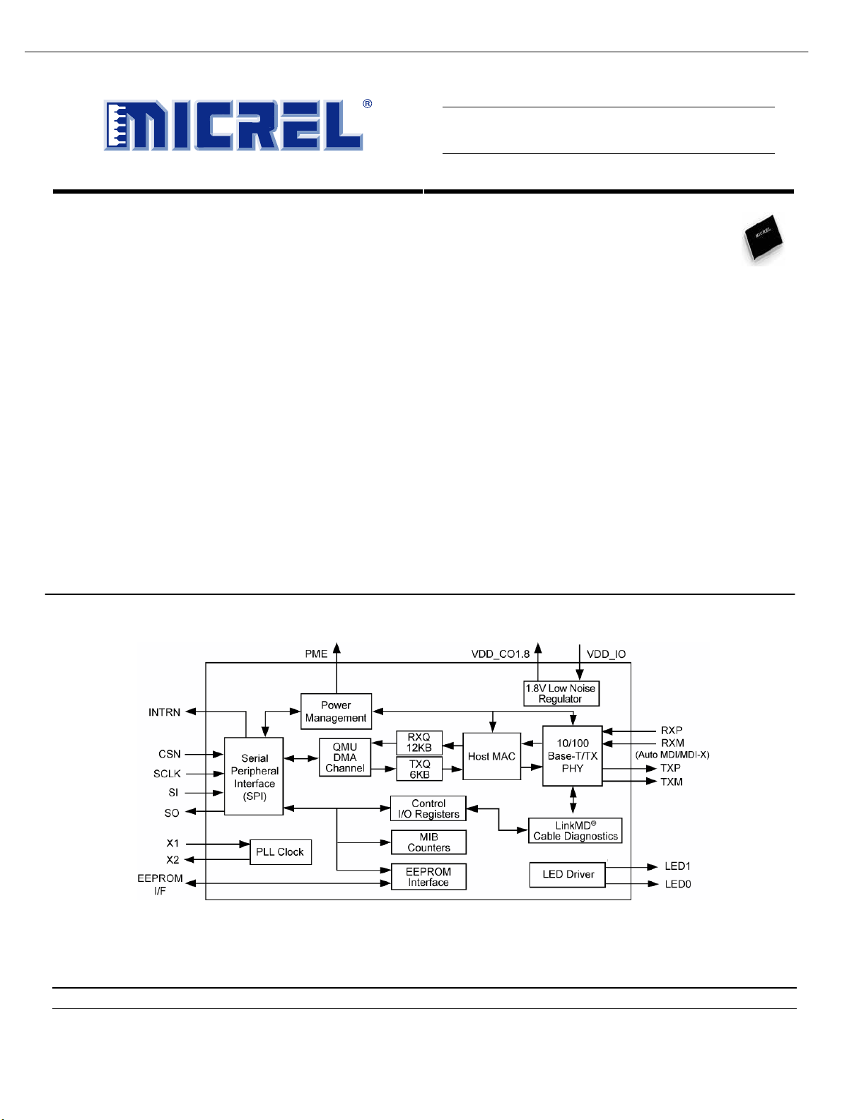
KSZ8851SNL/SNLI
Single-Port Ethernet Controller
with SPI Interface
Rev. 2.0
LinkMD is a registered trademark of Micrel, Inc.
Magic Packet is a trademark of Advanced Micro Devices, Inc.
MLF and MicroLeadFrame are registered tr ademarks of Amkor Techn ology, Inc.
Product names used in this datasheet are for identification purposes
only and may be trademarks of their respective companies.
Micrel Inc. • 2180 Fortune Drive • San Jose, CA 95131 • USA • tel +1 (408) 944-0800 • fax + 1 (408) 474-1000 • http://www.micrel.com
August 2009
M9999-083109-2.0
General Description
The KSZ8851SNL is a single-ch ip Fast Ethernet c ontroller
consisting of a 10/ 100 physical layer trans ceiver (PHY), a
MAC, and a Serial Peripheral Interface (SPI). The
KSZ8851SNL is des igned to enable an Ethernet network
connectivity with any host micro-controller equipped with
SPI interface. The KSZ8851SNL offers the most costeffective solution f or adding high-throughput Ethern et link
to traditional embedded systems with SPI interface.
The KSZ8851SNL is a single chip, mixed analog/digital
device offering Wake-on-LAN technology for effectively
addressing Fast Eth ernet a pplic ations. It cons ists of a F ast
Ethernet MAC contro ller, SPI interface and inc orporates a
unique dynamic memory pointer with 4-byte buffer
boundary and a fully utiliza ble 18KB for both TX (allocated
6KB) and RX (allocated 12KB) directions in host buffer
interface.
The KSZ8851SNL is designed to be fully compliant with
the appropriate IEEE 802.3 standards. An industrial
temperature-grade version of the KSZ8851SNL, the
KSZ8851SNLI is also a va il abl e (s ee “ Or der ing Inf or m atio n”
section).
LinkMD®
Physical signal transmission and rec eption are enhanced
through the use of analog circuitry, making the design
more efficient and a llowing for lower-power consum ption.
The KSZ8851SNL is designed using a low-power C MOS
process that features a single 3.3V power supply with
options for 1.8V, 2.5V or 3.3V VDD I/O. The device
includes an extensi ve feature set that off ers management
information base (MIB) counters and a fast SPI interface
with clock speed up to 40MHz.
The KSZ8851SNL includes unique cable diagnostics
feature called LinkMD
®
. This feature determ ines the length
of the cabling plant and als o ascertains if there is an open
or short condition in the cable. Accompanying software
enables the cable length and cable conditions to be
conveniently displayed. In addition, the KSZ8851SNL
supports Hewlett Packard (HP) Auto-MDIX thereby
eliminating the need to differentiate between straight or
crossover cables in applications.
Functional Diagram
Figure 1. KSZ8851SNL/SNLI Functional Diagram
AVR 2650 harman/kardon
150
Page 31

Micrel, Inc. KSZ8851SNL/SNLI
AVR 2650 harman/kardon
151
Features
Integra ted MA C and PH Y Ether net Control ler full y
compliant with IEEE 802.3/802. 3u sta ndar ds
SPI Interface with clock speeds up to 40MHz for high
throughput applications
Supports 10BASE-T/100BASE-TX
Supports IEEE 802.3x full-duplex flow control and half-
duplex backpressure collision flow control
Supports RXQ and TXQ FIFO DMA for fast data read
and write transfers
Supports IP Header (IPv4)/TCP/UDP/ICMP checksum
generation and checking
Supports IPv6 TCP/UDP/ICMP checksum generation
and checking
Automatic 32-bit CRC generation and checking
Supports simple command and data phases in SPI
cycle for RXQ/TXQ FIFO and registers read/write
Supports multiple data frames for TXQ FIFO and RXQ
FIFO without additional command phase
Supports flexible Byte (8-bit), Word (16-bit) and Double
word (32-bit) read/write access to internal registers
Larger internal memory with 12K Bytes for RX FIFO and
6K Bytes for TX FIFO. Programmable low, high and
overrun watermark for flow control in RX FIFO
Efficient architecture design with configurable host
interrupt schemes to minimize host CPU overhead and
utilization
Powerful and flexible address filtering scheme
Optional to use external serial EEPROM configuration
for MAC address
Single 25MHz reference clock for both PHY and MAC
HBM ESD Rating 6kV
Power Modes, Power Supplies, and Packaging
Single 3.3V power supply with options for 1.8V, 2.5V
and 3.3V VDD I/O
Built-in integrated 3.3V or 2.5V to 1.8V low noise
regulator (LDO) for core and analog blocks
Enhanced power management feature with energy
detect mode and soft power-down mode to ensure lowpower dissipation during device idle periods
Comprehensive LED indicator support for link, activity
and 10/100 speed (2 LEDs)
– User programmable
Low-power CMOS design
Commercial Temperature Range: 0oC to +70oC
Industrial Temperature Range: –40oC to +85oC
Available in 32-pin (5mm x 5mm) MLF® package
Additional Features
In addition to offering all of the features of a Layer 2
controller, the KSZ8851SNL offers:
Supports to add two-byte before frame header in order
for IP frame content with double word boundary
Micrel LinkMD
®
cable diagnostic capabilities to
determine cable length, diagnose faulty cables, and
determine distance to fault
Wake-on-LAN functionality
– Incorporates Magic Packet™, wake-up frame, network
link state, and detection of energy signal technology
HP Auto MDI-X™ crossover with disable/enable option
Ability to transmit and receive frames up to 2000 bytes
Network Features
10BASE-T and 100BASE-TX physical layer support
Auto- neg oti ati on: 10/1 00 M bps full and ha lf duplex
Adaptive equalizer
Baseline wander correction
Applications
Video/Audio Distribution Systems
Voice over IP (VoIP) and Analog Telephone Adapters
(ATA)
Building Automation
Home Base Control with Ethernet Connection
Industrial Control Sensor Devices (Temperature,
Pressure, Levels, and Valves)
Security, Motion Control and Surveillance Cameras
Markets
Fast Ethernet
Embedded Ethernet
Industrial Ethernet
Embedded Systems
August 2009
M9999-083109-2.0
Page 32

Micrel, Inc. KSZ8851SNL/SNLI
AVR 2650 harman/kardon
152
Pin Configuration
Figure 2. 32-Pin (5mm x 5mm) MLF®
August 2009
M9999-083109-2.0
Page 33

Micrel, Inc. KSZ8851SNL/SNLI
AVR 2650 harman/kardon
153
Pin Description
Pin Number Pin Name Type Pin Function
1 LED0 Opu
2 PME Opu Power Management Event (default active low)
3 INTRN Opu Interrupt Not
4 DGND Gnd Digital IO ground.
5 VDD_CO1.8 P 1.8V regulator output . This 1.8V output pi n provides power to pins 9 (VDD_A1.8) and 23
6 EED_IO Ipd/O In/Out Data from/to external EEPROM
7 EESK Opd EEPROM Serial Clock
8 AGND Gnd Analog ground.
9 VDD_A1.8 P 1.8V analog power supply from VDD_CO1.8 (pin 5) with appropriate filtering. If VDD_IO is
10 EECS Opd EEPROM Chip Select
11 RXP I/O Physical receive (MDI) or transmit (MDIX) signal (+ differential).
12 RXM I/O Physical receive (MDI) or transmit (MDIX) signal (– differential).
13 AGND Gnd Analog ground.
14 TXP I/O Physical transmit (MDI) or receive (MDIX) signal (+ differential).
15 TXM I/O Physical transmit (MDI) or receive (MDIX) signal (– differential).
16 VDD_A3.3 P 3.3V analog V
17 ISET O Set physical transmits output current.
18 AGND Gnd Analog ground.
19 RSTN Ipu Reset Not.
August 2009
M9999-083109-2.0
Programmable LED output to indicate PHY activity/status.
LED is ON when output is LOW; LED is OFF when output is HIGH.
LED indicators1 defined as follows:
Chip Global Control Register: CGCR bit [9]
0 (Default) 1
LED1 (pin 32) 100BT ACT
LED0 (pin 1) LINK/ACT LINK
Link (up) = LED On; Activity = LED Blink; Link/Act = LED On/Blink;
Speed = LED On (100BASE-T); LED Off (10BASE-T)
It is asserted (low or high depends on polarity set in PMECR register) when one of the
wake-on-LAN events is detected by KSZ8851SNL. The KSZ8851SNL is requesting the
system to wake up from low power mode.
An active low signal to host CPU to indicate an interrupt status bit is set. This pin needs
an external 4.7K pull-up resistor.
(VDD_D1.8) for core VDD supply.
If VDD_IO is set for 1.8V then this pin should be left floating, pins 9 (VDDA_1.8) and 23
(VDD_D1.8) will be sourced by the external 1.8V supply that is tied to pins 25 and 30
(VDD_IO) with appropriate filtering.
Config Mode: The pull-up/pull-down value is latched as with/without EEPROM during
power-up / reset. See “Strapping Options” section for details.
s (OBCR[1:0]=11 on-chip bus speed @ 25MHz) or 800ns (OBCR[1:0]=00 on-chip
A 4
bus speed @ 125 MHz) serial output clock to load configuration data from the serial
EEPROM.
1.8V, this pin must be supplied power from the same source as pins 25 and 30 (VDD_IO)
with appropriate filtering.
This signal is used to select an external EEPROM device.
input power supply with well decoupling capacitors.
DD
Pull-down this pin with a 3.01K 1% resistor to ground.
Page 34

Micrel, Inc. KSZ8851SNL/SNLI
AVR 2650 harman/kardon
154
Pin Number Pin Name Type Pin Function
Hardware reset pin (active Low). This reset input must be held low for a minimum of 10ms
after stable supply voltage 3.3V.
20 X1 I
21 X2 O
22 DGND Gnd Digital IO ground
23 VDD_D1.8 P 1.8V digital power supply from VDD_CO1.8 (pin 5) with appropriate filtering. If VDD_IO is
24 DGND Gnd Digital IO ground
25 VDD_IO P 3.3V, 2.5V or 1.8V digital V
26 CSN Ipu SPI slave mode: Chip Select Not
27 SO O SPI slave mode: Serial data out for SPI interface. This SO is tri-stated output when CSN
28 SCLK I SPI slave mode: Serial clock input for SPI interface. This clock speed can run up to
29 DGND Gnd Digital IO ground
30 VDD_IO P 3.3V, 2.5V or 1.8V digital V
31 SI Ipd SPI slave mode: Serial data in for SPI interface.
32 LED1 Opu Programmable LED1 output to indicate PHY activity/status (see LED0 description at pin1)
25MHz crystal or oscillator clock connection.
Pins (X1, X2) connect to a crystal. If an oscillator is used, X1 connects to a 3.3V tolerant
oscillator and X2 is a no connect.
Note: Clock requirement is +/- 50ppm for either crystal or oscillator.
1.8V, this pin must be supplied power from the same source as pins 25 and 30 (VDD_IO)
with appropriate filtering.
input power supply for IO with well decoupling capacitors.
DD
Active low input pin for SPI inte rface.
is negated and this pin must have external 4.7K pull-up to keep the SO line high while the
driver is tri-stated.
40MHz.
input power supply for IO with well decoupling capacitors.
DD
Legend:
P = Power supply Gnd = Ground
I/O = Bi-directional I = Input O = Output.
Ipd = Input with internal pull-down (58K +/-30%).
Ipu = Input with internal pull-up (58K +/-30%).
Opd = Output with internal pull-down (58K +/-30%).
Opu = Output with internal pull-up (58K +/-30%).
Ipu/O = Input with internal pull-up (58K +/-30%) during power-up/reset; output pin otherwise.
Ipd/O = Input with internal pull-down (58K +/-30%) during power-up/reset; output pin otherwise.
Strapping Options
Pin Number Pin Name Type Pin Function
6 EED_IO Ipd/O EEPROM select:
Pull-up = EEPROM present
Floating (NC) or Pull-down = EEPROM not present (default)
During power-up / reset, this pin value is latched into register CCR, bit 9
Note: Ipd/O = Input with internal pull-down (58K +/-30%) during power-up/reset; output pin otherwise.
Pin strap-ins are latched during power-up or reset.
August 2009
M9999-083109-2.0
Page 35

AVR 2650 harman/kardon
155
Page 36

AVR 2650 harman/kardon
156
1 Overview and Features
32-bit RISC Microcontroller – TX03 Series
TMPM333FDFG
TMPM333FYFG
TMPM333FWFG
1. Overview and Features
The TX03 series is a 32-bit RISC microcontroller series with an ARM CortexTM-M3 microcontroller
core.
Features of the TMPM333FDFG/FYFG/FWFG are as follows:
1.1 Features
(1) ARM Cortex-M3 microcontroller core
1) Improved code efficiency has been realized through the use of Thumb
New 16-bit Thumb instructions for improved program flow
New 32-bit Thumb instructions for improved performance
Auto-switching between 32-bit instruction and 16-bit instruction is executed by compiler.
-2 instruction
TMPM333
2) Both high performance and low power consumption have been achieved.
-High performance
A 32-bit multiplication (32×32=32 bit) can be executed with one clock.
Division takes between 2 and 12 cycles depending o n dividend and devisor
-Low power consumption
Optimized design using a low power consumption library
Standby function that stops the operation of the microcontroller core
3) High-speed interrupt response suitable for real-time control
An interruptible long instruction.
Stack push automatically handled by hardware.
Page 37

AVR 2650 harman/kardon
157
(2) On Chip program memory and data memory
Product name On chip Flash ROM On chip RAM
TMPM333FDFG 512Kbyte 32Kbyte
TMPM333FYFG 256Kbyte 16Kbyte
TMPM333FWFG 128Kbyte 8Kbyte
(3) 16-bit timer : 10 channels
16-bit interval timer mode
16-bit event counter mode
16-bit PPG output
Input capture function
(4) Real time clock (RTC) : 1 channel
Clock (hour , minute and second)
Calendar (Month, week, date and leap year)
Time correction or 30 seconds (by software)
Alarm (Alarm output)
Alarm interrupt
(5) Watchdog timer : 1 channel
26 cycles of binary counter
Watchdog timer out
(6) General-purpose serial interface : 3 channels
Either UART mode or synchronous mode can be selected (4byte FIFO equi pped)
(7) Serial bus interface : 3 channels
Either I
2C bus mode or synchronous mode can be selected.
(8) 10-bit A/D converter : 12 channels
Start by an internal or external timer trigger
Fixed channel/scan mode
Single/repeat mode
AD monitoring 2ch
Conversion speed 1.15usec(@fsys = 40MHz)
(9) Interrupt source
Internal: 38 factors…The order of precedence can be set over 7 levels (except the watchdog
timer interrupt).
External: 8 factors…The order of precedence can be set over 7 levels.
(10) Input/ output ports
79 pins
TMPM333
Page 38

AVR 2650 harman/kardon
158
1 Overview and Features
(11) Standby mode
Standby modes :IDLE, SLOW, SLEEP, STOP
Sub clock operation(32.768kHz) :SLOW, SLEEP
(12) Clock generator
On-chip PLL (quadru pled)
Clock gear function: The high-speed clock can be divided into 1/1, 1/2, 1/4 or 1/8.
(13) Endian
Little endian
(14) Maximum operating frequency
40MHz
(15) Operating voltage range
2.7V~3.6V (with on-chip regulator)
(16) Temperature range
-20~85 degrees (except during Flash writ ing/ erasing)
0~70 degrees (during Flash writing/ erasing)
(17) Package
LQFP100-P-1414-0.5H (14mm 14mm, 0.5mm pitch)
TMPM333
Page 39

AVR 2650 harman/kardon
159
TMPM333
1.2 Block Diagram
Cortex-M3
CPU
Debug
NVIC
SIO (3ch)
I2C (3ch)
FLASH
RAM
BOOT
ROM
I-Code
D-Code
System
I/F
AHB-Bus-Matrix
I/F
I/F
Bus Bridge
CG PORT A~K
TMRB (10ch)
IO-Bus
WDT
RTC
ADC (12ch)
Fig. 1-1 TMPM333 FDFG/FYFG/FWFG Block Diagram
Page 40

T
AVR 2650 harman/kardon
160
2 Pin Layout and Pin Functions
TMPM333
2 Pin Layout and Pin Functions
This chapter describes the pin layout, pin names and pin functions of TMPM333FDFG/
TMPM333FYFG/ TMPM333FWFG.
2.1 Pin Layout (Top view)
Fig.2-1 shows the pin layout of TMPM333FDFG/TMPM333FYFG/TMPM333FWF.
CTS0/ SCLK0/ PE2
CTS1/ SCLK1/ PE6
AN10/ PD6
AN11/ PD7
AVSS
VREFH
AVCC
INT4/ PG3
TB9OUT/ PK2
TB7OUT/ PJ5
TB2IN0/ PH4
TB2IN1/ PH5
TB8OUT/ PG7
TEST2
DVSS
DVCC
SDA2/ SO2/ PG4
SCL2/ SI2/ PG5
SCK2/ PG6
TEST1
INT5/ PF7
TXD0/ PE0
RXD0/ PE1
TXD1/ PE4
RXD1/ PE5
PD5 /AN9
PD4 /AN8
PD3 /AN7 /TB6IN1
PD2 /AN6 /TB6IN0
PD1 /AN5 /TB5IN1
100
5
10
15
20
25
30
PB3
SCK0/ PG2
SCL0/ SI0/ PG1
SDA0/ SO0/ PG0
BOOT/ TB0IN0/ PH0
PD0 /AN4 /TB5IN0
PC3 /AN3
PC2 /AN2
PC1 /AN1
PC0 /AN0
TEST4
PE3
95
90
TMPM333FDFG
TMPM333FYFG
TMPM333FWFG
Top View
35
PB4
TXD2/ PF0
RXD2/ PF1
TB0IN1/ PH1
TB1IN0/ PH2
TB1IN1/ PH3
CTS2/ SCLK2/ PF2
PJ4 /TB6OUT
PJ3 /INT3
PJ2 /INT2
PH7 /TB3IN1
PH6 /TB3IN0
85
40
PB5
INT6/ PJ6
TB0OUT/ PI0
TB1OUT/ PI1
TB2OUT/ PI2
PI7 /TB4IN1
RESET
MODE
NMI
PI6 /TB4IN0
80
45
PB6
PB7
SCK1/ PF6
SCL1/ SI1/ PF5
SDA1/ SO1/ PF4
XT2
XT1
75
70
65
60
55
50
PK0
INT1/ PJ1
TB3OUT/ PI3
REGVCC
REGVSS
X1
CVSS
X2
CVCC
PJ0 /INT0
PA7
PA6 /TRACEDATA3
PA5 /TRACEDATA2
PA4 /TRACEDATA1
PA3 /TRACEDATA0
PA2 /TRACECLK
DVSS
DVCC
PF3
PB2 /
PB1 /TDI
PJ7 /INT7
TEST3
PA1 /TCK /SWCLK
PA0 /TMS /SWDIO
PB0 /TDO /SWV
PI5 /TB5OUT
PI4 /TB4OUT
PK1 /SCOUT /ALARM
TRS
Fig.2-1 Pin Layout (LQFP100)
Page 41

AVR 2650 harman/kardon
161
Table2-1 Pin Numbers and Names (1/2)
Pin
No.
PD6, AN10
1
PD7, AN1 1
2
AVSS
3
VREFH
4
AVCC
5
PG3, INT4
6
PK2, TB9OUT
7
PJ5, TB7OUT
8
PH4, TB2IN0
9
PH5, TB2IN1
10
PG7, TB8OUT
11
TEST2
12
DVSS
13
DVCC
14
PG4, SO2, SDA2
15
PG5, SI2, SCL2
16
PG6, SCK2 42 PI2, TB2OUT
17
TEST1 43 PB6
18
PF7, INT5 44 PF4, SO1, SDA1
19
PE0, TXD0 45 PF5, SI1, SCL1
20
PE1, RXD0 46 PF6, SCK1
21
PE2, SCLK0, CTS0 47 PB7
22
PE4, TXD1 48 PI3, TB3OUT
23
PE5, RXD1 49 PJ1, INT1
24
PE6, SCLK1, CTS1 50 PK0,
25
Pin name Pin
t
Pin name
No.
PG0, SO0, SDA0
26
PG1, SI0, SCL0
27
PG2, SCK0
28
PB3
29
30
PH0, TB0IN0,
PH1, TB0IN1
31
PH2, TB1IN0
32
PF0, TXD2
33
PF1, RXD2
34
PF2, SCLK2, CTS2
35
PH3, TB1IN1
36
PB4
37
PI0, TB0OUT
38
PJ6, INT6
39
PI1, TB1OUT
40
PB5
41
BOOT
TMPM333
Page 42

AVR 2650 harman/kardon
162
2 Pin Layout and Pin Functions
Pin
No.
51
PK1, SCOUT,
PI4, TB4OUT 77 XT1
52
PI5, TB5OUT 78 XT2
53
PB0, TDO, SWV 79 PI6, TB4IN0
54
P A0, TMS, SWDIO 80
55
P A1, TCK, SWCLK 81 MODE
56
TEST3 82
57
PJ7, INT7 83 PI7, TB4IN1
58
PB1, TDI 84 PH6, TB3IN0
59
60
PB2,
TRST
PF3 86 PJ2, INT2
61
DVCC 87 PJ3, INT3
62
DVSS 88 PJ4, TB6OUT
63
P A2, TRACECLK 89 PE3
64
P A3, TRACEDAT A0 90 TEST4
65
P A4, TRACEDAT A1 91 PC0, AN0
66
P A5, TRACEDAT A2 92 PC1, AN1
67
P A6, TRACEDAT A3 93 PC2, AN2
68
PA7 94 PC3, AN3
69
PJ0, INT0 95 PD0, AN4, TB5IN0
70
CVCC 96 PD1, AN5, TB5IN1
71
X2 97 PD2, AN6, TB6IN0
72
CVSS 98 PD3, AN7, TB6IN1
73
X1 99 PD4, AN8
74
REGVSS 100 PD5, AN9
75
Pin name Pin
ALARM
Under development
Table2-1 Pin Numbers and Names (2/2)
No.
76 REGVCC
NMI
RESET
85 PH7, TB3IN1
Pin name
TMPM333
Page 43

AVR 2650 harman/kardon
163
Under development
TMPM333
2.2 Pin names and Functions
Table2-2 and Table2-3 sort the input and output pins of the TM
TMPM333FWFG by pin or port. Each table includes alternate pin names and functions for multi-function pins.
2.2.1 Sorted by Pin
Table2-2 Pin Names and Functions Sorted by Pin (1/5)
Type
Function
PS
Function
Test
PS
Function
Test
Function
# of
Pins
1
2
Pin Name
PD6
AN10
PD7
AN11
3 AVSS I
4 VREFH I
5 AVCC I
PG3
6
INT4
PK2
7
TB9OUT
PJ5
8
TB7OUT
PH4
9
TB2IN0
PH5
10
TB2IN1
PG7
11
TB8OUT
12 TEST2 - TEST pin: Not connected. - - 13 DVSS - GND pin - - 14 DVCC - Power supply pin - - -
PG4
15
SDA2/
SO2
PG5
16
SCL2/
SI2
PG6
SCK2
17
18 TEST1 -
PF7
19
INT5
Input/
Output
I
I
I
I
Input port
Analog input
Input port
Analog input
A/D converter: GND pin (0V)
Tie AVSS to power supply even if the A/D
converter is not used.
Supplying the A/D converter with a
reference power supply.
Tie VREFH to power supply even if the
A/D converter is not used.
Supplying the A/D converter with a power
supply. Tie AVCC to power supply even if
the A/D converter is not used.
I/O I I/O port
Interrupt request pin
I/O O I/O port
Timer B output
I/O I I/O port
Timer B output
I/O I I/O port
Inputting the timer B capture trigger
I/O I I/O port
Inputting the timer B capture trigger
I/O O I/O port
Timer B output
I/O
I/O
O
I/O
I/O
I
I/O
I/O
I/O port
If the serial bus interface operates
-in the I2C mode : data pin
-in the SIO mode: data pin
I/O port
If the serial bus interface operates
-in the I2C mode : clock pin
-in the SIO mode: data pin
I/O port
Inputting and outputting a clock if the
serial bus interface operates in the SIO
mode.
TEST pin: Not connected.
I/O
I
I/O port
Interrupt request pin
Function
PM333FDFG/ TMPM333FYFG/
Programma
ble Pull up/
Pull down
Schmitt
trigger
Programm
able Open
Drain
Output
Pull up - Pull up - -
- - -
- - -
- - -
Pull up
w/ noise filter
Pull up - Pull up - -
Pull up
Pull up
Pull up -
Pull up
Pull up
Pull up
-
-
- - -
Pull up
w/ noise filter
Page 44

AVR 2650 harman/kardon
164
2 Pin Layout and Pin Functions
Table2-2 Pin Names and Functions Sorted by Pin (2/5)
Type
Function
# of
Pins
20
21
22
23
24
25
26
27
28
Pin Name
PE0
TXD0
PE1
RXD0
PE2
SCLK0
CTS0
PE4
TXD1
PE5
RXD1
PE6
SCLK1
CTS1
PG0
SDA0/
SO0
PG1
SCL0/
SI0
PG2
SCK0
Input/
Output
I/O
O
I/O
I
I/O
I
I
I/O
O
I/O
I
I/O
I
I
I/O
I/O
O
I/O
I/O
I
I/O
I/O
29 PB3 I/O I/O port
Function/
Control
Function
30
31
32
33
34
35
36
PH0
TB0IN0
BOOT
PH1
TB0IN1
PH2
TB1IN0
PF0
TXD2
PF1
RXD2
PF2
SCLK2
CTS2
PH3
TB1IN1
I/O
I
I
I/O
I
I/O
I
I/O
O
I/O
I
I/O
I
I
I/O
I
37 PB4 I/O I/O port
38
39
PI0
TB0OUT
PJ6
INT6
I/O
O
I/O
I
I/O port
Sending serial data
I/O port
Receiving serial data
I/O port
Serial clock input/ output
Handshake input pin
I/O port
Sending serial data
I/O port
Receiving serial data
I/O port
Serial clock input/ output
Handshake input pin
I/O port
If the serial bus interface operates
-in the I2C mode : data pin
-in the SIO mode: data pin
I/O port
If the serial bus interface operates
-in the I2C mode : clock pin
-in the SIO mode: data pin
I/O port
Inputting and outputting a clock if the
serial bus interface operates in the SIO
mode.
I/O port
Inputting the timer B capture trigger
Setting a single boot mode: This pin
goes into single boot mode by sampling
"L" at the rise of a reset signal.
I/O port
Inputting the timer B capture trigger
I/O port
Inputting the timer B capture trigger
I/O port
Sending serial data
I/O port
Receiving serial data
I/O port
Serial clock input/ output
Handshake input pin
I/O port
Inputting the timer B capture trigger
I/O port
Timer B output
I/O port
Interrupt request pin
Under development
Function
Programm
able
Pull-up/
Pull down
Pull up
Pull up
Pull up
Pull up
Pull up
Pull up
Pull up
Pull up
Pull up
Pull up
Pull up
Pull up
Pull up
Pull up
Pull up
Pull up
Pull up
Pull up
Pull up
Pull up
TMPM333
Schmitt
trigger
w/ noise filter
Programma
ble Open
Drain
Output
-
-
- -
-
-
-
-
-
- -
- -
Page 45

T
AVR 2650 harman/kardon
165
Type
Function
Function/
Debug
Test
Function
Function/
Debug
Function
PS
Table2-2 Pin Names and Functions Sorted by Pin (3/5)
# of
Pins
40
Pin Name
PI1
TB1OUT
Input/
Output
I/O O I/O port
Timer B output
41 PB5 I/O I/O port
42
PI2
TB2OUT
I/O O I/O port
Timer B output
43 PB6 I/O I/O port
44
45
46
PF4
SDA1/
SO1
PF5
SCL1/
SI1
PF6
SCK1
I/O
I/O
O
I/O
I/O
I
I/O
I/O
I/O port
If the serial bus interface operates
-in the I2C mode : data pin
-in the SIO mode: data pin
I/O port
If the serial bus interface operates
-in the I2C mode : clock pin
-in the SIO mode: data pin
I/O port
Inputting and outputting a clock if the
serial bus interface operates in the SIO
mode.
47 PB7 I/O I/O port
48
49
PI3
TB3OUT
PJ1
INT1
I/O O I/O port
Timer B output
I/O I I/O port
Interrupt request pin
50 PK0 I/O I/O port -
PK1
SCOUT
51
ALARM
PI4
52
TB4OUT
PI5
53
TB5OUT
PB0
54
TDO/SWV
PA0
55
TMS/SWDIO
PA1
56
TCK/
SWCLK
I/O
O
O
I/O O I/O port
I/O O I/O port
I/O O I/O port
I/O
I/O
I/O
I
I/O port
System clock output
Alarm output
Timer B output
Timer B output
Debug pin
I/O port
Debug pin
I/O port
Debug pin
57 TEST3 - TEST pin: Not connected.
58
59
60
PJ7
INT7
PB1
TDI
PB2
TRS
I/O I I/O port
Interrupt request pin
I/O I I/O port
Debug pin
I/O
I
I/O port
Debug pin
61 PF3 I/O I/O port
62 DVCC - Power supply pin
63 DVSS - GND pin
Under development
Function
Programmab
le Pull-up/
Pull down
Pull up
Pull up
Pull up
Pull up
Pull up
Pull up
Pull up
Pull up
Pull up
Pull up
Pull up
Pull up
Pull up
Pull up
Pull up
Pull up
-
Pull up
Pull up
Pull up
Pull up
-
-
TMPM333
Programmab
Schmitt
trigger
- -
- -
- -
- -
- -
- -
w/ noise filter
- -
- -
- -
- -
- -
- -
w/ noise filter
- -
- -
- -
le Open
Drain
Output
(Note 4)
-
-
Page 46

AVR 2650 harman/kardon
166
2 Pin Layout and Pin Functions
Table2-2 Pin Names and Functions Sorted by Pin (4/5)
Type
Function/
Debug
# of
Pins
64
65
66
67
68
Pin Name
PA2
TRACECLK
PA3
TRACEDATA0
PA4
TRACEDATA1
PA5
TRACEDATA2
PA6
TRACEDATA3
Input/
Output
I/O
O
I/O
O
I/O
O
I/O
O
I/O
O
69 PA7 I/O I/O port Pull up
Function
PS
Clock
PS
Clock
PS
Clock
Function
Control
Function
70
PJ0
INT0
I/O
I
71 CVCC - Power supply pin
72 X2 O Connected to a high-speed oscillator.
73 CVSS - GND pin
74 X1 I Connected to a high-speed oscillator.
75 REGVSS - GND pin
76 REGVCC - Power supply pin
77 XT1 I Connected to a low-speed oscillator.
78 XT2 O Connected to a low-speed oscillator.
79
80
PI6
TB4IN0
NMI
I/O
I
I Non-maskable interrupt
81 MODE I Mode pin: Tied to GND pin
RESET
PI7
TB4IN0
PH6
TB3IN0
PH7
TB3IN1
PJ2
INT2
PJ3
INT3
I Reset input pin
I/O
I
I/O
I
I/O
I
I/O
I
I/O
I
82
83
84
85
86
87
I/O port
Debug pin
I/O port
Debug pin
I/O port
Debug pin
I/O port
Debug pin
I/O port
Debug pin
I/O port
Interrupt request pin
I/O port
Inputting the timer B capture trigger
I/O port
Inputting the timer B capture trigger
I/O port
Inputting the timer B capture trigger
I/O port
Inputting the timer B capture trigger
I/O port
Interrupt request pin
I/O port
Interrupt request pin
Under development
Function
Programma
ble Pull-up/
Pull down
Pull up
Pull up
Pull up
Pull up
Pull up
Pull up
-
-
-
-
-
-
-
-
Pull up
-
-
Tied to
Pull up
Pull up
Pull up
Pull up
Pull up
Pull up
TMPM333
Programmab
Schmitt
trigger
- -
- -
- -
- -
- -
w/ noise filter
- -
- -
- -
-
- -
- -
-
- -
-
w/ noise filter
-
w/ noise filter
-
-
-
w/ noise filter
w/ noise filter
le Open
Drain
Output
-
-
Test
88
PJ4
TB6OUT
I/O
O
I/O port
Timer B output
89 PE3 I/O I/O port
90 TEST4 - TEST pin: Not connected.
Pull up
Pull up
-
- -
- -
Page 47

AVR 2650 harman/kardon
167
Under development
TMPM333
Table2-2 Pin Names and Functions Sorted by Pin (5/5)
Programma
ble Open
Drain
Output
Type
Function
# of
Pins
91
92
93
94
95
96
97
98
99
100
Pin Name
PC0
AN0
PC1
AN1
PC2
AN2
PC3
AN3
PD0
AN4
TB5IN0
PD1
AN5
TB5IN1
PD2
AN6
TB6IN0
PD3
AN7
TB6IN1
PD4
AN8
PD5
AN9
Input/
Output
I
I
I
I
I
I
I
I
I
I
I
I
I
I
I
I
I
I
I
I
I
I
I
I
Function
Input port
Analog input
Input port
Analog input
Input port
Analog input
Input port
Analog input
Input port
Analog input
Inputting the timer B capture trigger
Input port
Analog input
Inputting the timer B capture trigger
Input port
Analog input
Inputting the timer B capture trigger
Input port
Analog input
Inputting the timer B capture trigger of
Input port
Analog input
Input port
Analog input
Programma
ble Pull-up/
Pull down
Schmitt
trigger
Pull up - Pull up - Pull up - Pull up - -
Pull up - -
Pull up - -
Pull up - -
Pull up - -
Pull up - Pull up - -
(Note 1) TEST1 through 4 must be left unconnected.
(Note 2) Be sure to tie MODE to GND.
(Note 3) Tie VREFH/ AVCC to power supply and AVSS to GND even if the A/D converter is not used.
(Note 4) Nch open drain port.
(Note 5) The noise elimination width of the noise filter is approximately 30 ns under typical
conditions.
Page 48

AVR 2650 harman/kardon
168
TC74VHC153F/FN/FT/FK
TOSHIBA CMOS Digital Integrated Circuit Silicon Monolithic
TC74VHC153F,TC74VHC153FN,TC74VHC153FT,TC74VHC153FK
Dual 4-Channel Multiplexer
The TC74VHC153 is an advanced high speed CMOS DUAL
4-CHANNEL MULTIPLEXERs fabricated with silicon gate
2
C
MOS technology.
It achieves the high speed operation similar to equivalent
Bipolar Schottky TTL while maintaining the CMOS low power
dissipation.
Each of these data (1C0-1C3, 2C0-2C3) is selected by the two
address inputs A and B.
Separate strobe inputs (
two four-line sections.
The strobe input (
the output is fixed in low level while the strobe input is held
high.
An input protection circuit ensures that 0 to 5.5 V can be
applied to the input pins without regard to the supply voltage.
This device can be used to interface 5 V to 3 V systems and two
supply systems such as battery back up. This circuit prevents
device destruction due to mismatched supply and input voltages.
G1
, G2) are provided for each of the
G
) can be used to inhibit the data output;
Features
• High speed: t
• Low power dissipation: I
• High noise immunity: V
• Power down protection is provided on all inputs.
• Balanced propagation delays: t
• Wide operating voltage range: V
• Pin and function compatible with 74ALS153
= 5.0 ns (typ.) at VCC = 5 V
pd
= 4 μA (max) at Ta = 25°C
CC
NIH
= V
= 28% VCC (min)
NIL
∼
t
−
pLH
CC (opr)
pHL
= 2 to 5.5 V
Note: xxxFN (JEDEC SOP) is not available in
Japan.
TC74VHC153F
TC74VHC153FN
TC74VHC153FT
TC74VHC153FK
Weight
SOP16-P-300-1.27A : 0.18 g (typ.)
SOL16-P-150-1.27 : 0.13 g (typ.)
TSSOP16-P-0044-0.65A : 0.06 g (typ.)
VSSOP16-P-0030-0.50 : 0.02 g (typ.)
Page 49

A
AVR 2650 harman/kardon
169
TC74VHC153F/FN/FT/FK
Pin Assignment IEC Logic Symbol
(14)
G1
B
1C3
1C2
1C1
1C0
1Y
GND
Truth Table
V
1
2
3
4
5
6
7
8
(top view)
15
14
13
12
11
10
9
CC
G2
2C3
2C2
2C1
2C0
2Y
16
A
B
G1
1C0
1C1
1C2
1C3
G2
2C0
2C1
2C2
2C3
(2)
(1)
(6)
(5)
(4)
(3)
(15)
(10)
(11)
(12)
(13)
0
1
EN
0
1
2
3
G
0
3
MUX
(7)
(9)
1Y
2Y
Select Inputs Data Inputs Strobe Output
B A C0 C1 C2 C3 G Y
X X X X X X H L
L L L X X X L L
L L H X X X L H
L H X L X X L L
L H X H X X L H
H L X X L X L L
H L X X H X L H
H H X X X L L L
H H X X X H L H
X: Don’t care
Page 50

A
AVR 2650 harman/kardon
170
TC74VHC153F/FN/FT/FK
System Diagram
14
2
B
S0
0S
S1
1S
S2
2S
S3
3S
1C0
1C1
1C2
1C3
G1
2C0
2C1
2C2
2C3
G2
6
5
4
3
1
10
11
12
13
15
S0
S1
S2
S3
Same as above block
7
1Y
9
2Y
Page 51

AVR 2650 harman/kardon
171
CS49DV8C Data Sheet
FEATURES
• 32-bit Post-Processor Audio DSP supports Multichannel
®
Dolby
Volume
Programmable through DSP Composer
•
™
• CS49DV8, supports up to 7.1 Channels of Dolby Volume
processing at 48 kHz, 44.1 kHz or 32 kHz.
— Input Configurable for all input/o utp ut d igi t al au dio types
2
(I
S, LJ/RJ, and TDM)
— 32-bit data path delivers uncomp rom is ed dy nam ic rang e
— 192 kHz capable integrated S/PDIF transmitter
— DAO can operate in master or slave mode (SCLK &
LRCLK)
• Integrated Clock Manager/PLL
— Capable of operating from a wide variety of external
crystals or external oscillators
• Input Fs Auto Detection, Reporting and Handling
• Sample rate conversion.
• Master & Slave Host Boot Capability via Serial Interface
• SPI interface capable of running up to 25 MHz during run
time
• 1.8V Core and a 3.3V I/O that is tolerant to 5V input
The new CS49DV8C is the fastest time-to-market, massproduction ready Multichannel Dolby Volume solution available.
The target applications for the CS49DV8C DSP are:
— Soundbars
— DTVs with Integrated Soundbars
— HDTV Stands/Furniture with Integrated Soundbars
— Automotive Head Units
— Automotive Outboard Amplifiers
— Blu-ray Disc
All of these applications and many more that use volume control
and are subject to playback from sources that do not have consistent volume levels will benefit from the CS49DV8C Dolby Volume
solution.
32-bit Dual Audio DSP Engine
featuring Multichannel Dolby
®
& DVD Receivers / HTiBs
®
Volume
Serial
Control 1
8 Ch. Audio In
S/PDIF
S/PDIF
8 Ch PCM
Audio Out
Preliminary Product Information
Ordering Information
See page 27 for ordering information.
Serial
Control 2
32-bit
DSP A
P
X Y P X Y
Ext. Memory Controller
D
M
A
32-bit
DSP B
GPIOUART Debug
This document contains information for a new product.
Cirrus Logic reserves the right to modify this product without notice.
STC
TMR1
TMR2
PLL
Copyright 2008 Cirrus Logic (All Rights Reserved) SEPT ‘08
DS868PP2
http://www.cirrus.com
Page 52

#
1
0
1
2
3
4
5
G
2
G
AVR 2650 harman/kardon
172
CS49DV8C Data Sheet
32-bit Audio DSP Family
8. Device Pin-Out Diagram
8.1 128-Pin LQFP Pin-Out Diagram
VDD6
GND6
GPIO38, PCP_WR# / DS#, SCP2_CLK
GPIO11, PCP_A3, AS#, SCP2_MISO / SDA
GPIO10, PCP_A2 / A10, SCP2_MOSI
GPOI9, SCP1_IRQ#
GPIO8, PCP_IRQ#, SCP2_IRQ#
GPIO7, SCP1_CS#, IOWAIT
GPIO6, PCP_CS#, SCP2_CS#
GPIO14, DAI1_DATA3, TM3, DSD3
GPIO13, DAI1_DATA2, TM2, DSD2
GPIO12, DAI1_DATA1, TM1, DSD1
PIO42, BDI_REQ# , DAI2_LRCLK, PCP_IRQ# / BSY#
GPIO43, BDI_CLK, DAI2_SCLK
BDI_DATA, DAI2_DATA, DSD5
GPIO26, DAO2_DATA3 / XMTB/UART_TX_EN
GPIO20, DAO2_DATA2, EE_CS#
VDDIO7
GNDIO7
GPIO3, DDAC
GPIO2, UART_TXD
VDD7
GPIO1, UART_RXD
GPIO0, UART_CLK
GND7
XTAL_OUT
XTI
XTO
GNDA
PLL_REF_RES
VDDA (3.3V)
VDD8
GND8
DAI1_DATA0, TM0, DSD0
VDDIO8
DAI1_SCLK, DSD-CLK
DAI1_LRCLK, DSD4
GNDIO8
DBDA
DBCK
GPIO37, SCP1_BSY#, PCP_BSY
1
5
10
15
20
25
30
35
GPIO34, SCP1__MISO / SDA
GPIO35, SCP1_CLK
125
40
GPIO33, SCP1_MOSI
VDDIO6
GNDIO6
EXT_CS1#
RESET#
EXT_OE#
120
128-Pin LQFP
45
GND5
EXT_A18
EXT_A19
115
50
VDD5
SD_RAS#
SD_CS#
EXT_A15
EXT_A16
EXT_A17
110
55
GNDIO5
SD_CAS#
SD_WE#
SD_BA1, EXT_A14
60
105
SD_BA0, EXT_A13
SD_A10, EXT_A10
100
95
90
85
80
75
70
65
SD_A0, EXT_A0
SD_A1, EXT_A1
VDDIO5
SD_A2, EXT_A 2
GND4
SD_A3, EXT_A 3
SD_A4, EXT_A 4
VDD4
EXT_CS2#
SD_A5, EXT_A 5
GNDIO4
SD_A6, EXT_A 6
SD_A7, EXT_A 7
VDDIO4
SD_A8, EXT_A 8
SD_A9, EXT_A 9
GND3
SD_A11, EXT_A1
SD_A12, EXT_A1
VDD3
SD_CLKEN
SD_CLKIN
SD_CLKOUT
SD_DQM1
SD_D8, EXT_D 8
SD_D9, EXT_D 9
GNDIO3
SD_D10, EXT_D1
SD_D11, EXT_D1
VDDIO3
SD_D12, EXT_D1
SD_D13, EXT_D1
SD_D14, EXT_D1
SD_D15, EXT_D1
SD_D0, EXT_D 0
GNDIO2
EXT_WE#
SD_D1, EXT_D1
TEST
VDD1
GND1
DAO_MCLK
GPIO19, DAO2_DATA1, HS4
GPIO23,
DAO2_LRCLK
GPIO22, DAO2_SCLK
GPIO18, DAO2_DATA0, HS3
VDDIO1
DAO1_DATA0, HS0
GPIO16, DAO1_DATA2, HS2
GPIO15, DAO1_DATA1, HS1
PIO17, DAO1_DATA3 / XMTA
DAO1_SCLK
VDD2
DAO1_LRCLK
GND2
SD_DQM0
SD_D7, EXT_D7
GNDIO1
VDDIO2
SD_D6, EXT_D6
SD_D5, EXT_D5
SD_D4, EXT_D4
SD_D3, EXT_D3
SD_D2, EXT_D2
Figure 15. 128-Pin LQFP Pin-Out
28 Copyright 2008 Cirrus Logic, Inc. DS868PP2
Page 53

AVR 2650 harman/kardon
173
TC74HC151AP/AF/AFN
TOSHIBA CMOS Digital Integrated Circuit Silicon Monolithic
TC74HC151AP,TC74HC151AF,TC74HC151AFN
8-Channel Multiplexer
The TC74HC151A is a high speed CMOS 8-CHANNEL
MULTIPLEXER fabricated with silicon gate C2MOS technology.
It achieves the high speed operation similar to equivalent
LSTTL while maintaining the CMOS low power dissipation.
One of eight date input signals (D0-D7) is selected by decoding
of the three-bit address input (A, B, C). The selected data appears
on two outputs: non-inverting (Y) and inverting (W).
The strobe input provides two output conditions; a low level on
the strobe input transfers the selected data to the outputs. A high
level on the strobe input sets the Y output low and the W output
high without regard to the data or select input conditions.
All inputs are equipped with protection circuits against static
discharge or transient excess voltage.
Features
Note: xxxFN (JEDEC SOP) is not available in
Japan.
TC74HC151AP
TC74HC151AF
• High speed: t
• Low power dissipation: I
• High noise immunity: V
• Output drive capability: 10 LSTTL loads
• Symmetrical output impedance: |I
Balanced propagation delays: t
•
• Wide operating voltage range: V
• Pin and function compatible with 74LS151
= 15 ns (typ.) at VCC = 5 V
pd
= 4 μA (max) at Ta = 25°C
CC
NIH
= V
= 28% VCC (min)
NIL
OH
∼
t
−
pLH
(opr) = 2 to 6 V
CC
| = IOL = 4 mA (min)
pHL
Pin Assignment
TC74HC151AFN
Weight
DIP16-P-300-2.54A : 1.00 g (typ.)
SOP16-P-300-1.27A : 0.18 g (typ.)
SOL16-P-150-1.27 : 0.13 g (typ.)
Page 54

*
1
AVR 2650 harman/kardon
174
Sound Processors for Home Theater Systems
2ch
Electronic Volume
BD3812F
No.10081EAT03
Description
BD3812F is an electronic volume having volume, gain amplifier functions necessary for applications in AV receivers, home
theatre systems, min-component systems and so forth. Having a chip select terminal, it can be controlled until 4 chips with
common bus line.
Features
1) Residual noise : 1.2µVrms {dynamic range : 131dB (IHF-A)}
2) 2ch independent volume (0 to -103dB, MUTE 1dB/step)
3) 8ch at maximum available in combination of any of BD3811K1, BD3813KS, BD3814FV, BD3815KS (6ch volume)
in common bus line
4) It can be controlled until 4 chips with common bus line at the same time
5) Maximum output voltage : 4.2Vrms (Vcc=7, VEE=-7V, RL=10k
)
6) 2-line serial control (for both 3.3V and 5V)
7) Built-in Output gain amplifier for adjustment of output signal voltage (0, 6 to 18dB, 2dB/step)
8) Output mute controllable by serial data and external control terminal
Applications
AV receivers, home theater systems, mini-component systems, etc.
Absolute maximum ratings (Ta=25)
Parameter Symbol Ratings Unit
Powewr supply voltage
VCC 7.5
VEE -7.5
V
Input signal voltage VIN VCC+0.3 to VEE-0.3 V
Power dissipation Pd 450*2 mW
Operating temperature range Topr
Storage temperature range Tastg
*1 Even in the specified range of Power Supply Voltage, applying voltage only to the VCC side may
cause an excessive current to give a permanent damage to the IC.
When starting up power supplies, VEE and VCC should be powered on simultaneously or VEE first; then followed by VCC.
*2 Over Ta
25°C, reduce at the rate of 4.5mW/°C. When installed on the standard board (size: 70x70x1.6mm).
20 to +75
55 to +125
Operating conditions
It must function normally at Ta25°C.
Parameter Symbol
Operating source voltage
Min. Typ. Max.
VCC 5 7 7.3
VEE -7.3 -7 -5
Ratings
Unit
V
Page 55

AVR 2650 harman/kardon
175
●Application circuit
IN1
10µ
1
AGND
2
IN2
10μ
3
AGND
4
VEE
AGND
VCC
5
47μ
6
47µ
7
●Reference data
2.5
2
1.5
1
0.5
0
-0.5
-1
-1.5
-2
CIRCUIT CURRENT (mA)
-2.5
0246810
POWER SU PPLY (V)
Fig.3 Circuit current - Power supply
VCC
VEE
10
1
0.1
0.01
THD+N (%)
0.001
0.0001
0.001 0.01 0.1 1 10
INPUT VOLTAGE (Vrms)
Fig.6 THD+N - Input voltage
BD3812F
Fig.2
10
8
6
4
2
0
-2
GAIN(dB)
-4
-6
-8
-10
10 100 1000 10000 100000
FREQUENCY (Hz)
Fig.4 Voltage gain - Frequency
20
15
10
5
GAIN (dB)
0
-5
10 100 1000 10000 100000
FREQUENCY (Hz)
Fig.7 Output gain - Frequency
LOGIC
0, 6~18dB
2dB/step
14
13
12
OUT1
OUT2
SEL
11
DGND
10
9
8
MUTE
DA
CL
UNIT
RESISTOR :Ω
CAPACITO R : F
10
1
0.1
0.01
OUT PUT VOLT AGE (Vrms )
0.001
0.001 0.01 0.1 1 10
IN PU T VOLTAGE (Vrms)
Fig.5 Output voltage - Input voltage
Page 56

AVR 2650 harman/kardon
176
T5CN5
32-bit RISC Microcontroller – TX03 Series
T5CN5
Overview and Features
The TX03 series is a 32-bit RISC microcontroller series with an ARM CortexTM-M3 microcontroller
core.
Features of the T5CN5 is as follows:
1.1 Features
(1) ARM Cortex-M3 microcontroller core
1) Improved code efficiency has been realized through the use of Thumb2 instruction
New 16-bit Thumb instructions for improved program flow
New 32-bit Thumb instructions for improved performance
Auto-switching between 32-bit instruction and 16-bit instruction is executed by compiler.
2) Both high performance and low power consumption have been achieved.
-High performance
A 32-bit multiplication (32×32=32 bit) can be executed with one clock.
Division takes between 2 and 12 cycles depending o n dividend and devisor
-Low power consumption
Optimized design using a low power consumption library
Standby function that stops the operation of the microcontroller core
3) High-speed interrupt response suitable for real-time control
An interruptible long instruction.
Stack push automatically handled by hardware.
Page 57

AVR 2650 harman/kardon
177
(2) On Chip program memory and data memory
Product name On chip Flash ROM On chip RAM
T5CN5 512Kbyte 32Kbyte
(3) 16-bit timer : 10 channels
16-bit interval timer mode
16-bit event counter mode
16-bit PPG output
Input capture function
(4) Real time clock (RTC) : 1 channel
Clock (hour , minute and second)
Calendar (Month, week, date and leap year)
Time correction or 30 seconds (by software)
Alarm (Alarm output)
Alarm interrupt
(5) Watchdog timer : 1 channel
26 cycles of binary counter
Watchdog timer out
(6) General-purpose serial interface : 3 channels
Either UART mode or synchronous mode can be selected (4byte FIFO equi pped)
(7) Serial bus interface : 3 channels
Either I
2C bus mode or synchronous mode can be selected.
(8) CEC : 1 channel
Transmis sion and reception per byte.
(9) Remote control signal preprocessor : 2 channels
Can receive up to 72bit data at a time
(10) 10-bit A/D converter : 12 channels
Start by an internal or external timer trigger
Fixed channel/scan mode
Single/repeat mode
AD monitoring 2ch
Conversion speed 1.15usec(@fsys = 40MHz)
(11) Interrupt source
Internal: 42 factors…The order of precedence can be set over 7 levels (except the watchdog
timer interrupt).
External: 8 factors…The order of precedence can be set over 7 levels.
(12) Input/ output ports
79 pins
T5CN5
Page 58

AVR 2650 harman/kardon
178
(13) Standby mode
Standby modes :IDLE, SLOW, SLEEP, STOP
Sub clock operation(32.768kHz) :SLOW, SLEEP
(14) Clock generator
On-chip PLL (quadru pled)
Clock gear function: The high-speed clock can be divided into 1/1, 1/2, 1/4 or 1/8.
(15) Endian
Little endian
(16) Maximum operating frequency
40MHz
(17) Operating voltage range
2.7V~3.6V (with on-chip regulator)
(18) Temperature range
-20~85 degrees (except during Flash writ ing/ erasing)
0~70 degrees (during Flash writing/ erasing)
(19) Package
LQFP100-P-1414-0.5H (14mm 14mm, 0.5mm pitch)
T5CN5
Page 59

AVR 2650 harman/kardon
179
T5CN5
1.2 Block Diagram
Cortex-M3
CPU
Debug
NVIC
SIO (3ch)
I2C (3ch)
Remote control signal
preprocessor (2ch)
CG
CEC
I-Code
D-Code
S
ystem
Bus Bridge
AHB-Bus-Matrix
IO-Bus
I/F
FLASH
I/F
I/F
BOOT
PORT 0~A
TMRB (10ch)
WDT
RTC
ADC (12ch)
RAM
ROM
Fig. 1.1 T5CN5 Block Diagram
Page 60

T
AVR 2650 harman/kardon
180
T5CN5
2. Pin Layout and Pin Functions
This chapter describes the pin layout, pin names and pin functions of T5CN5.
2.1 Pin Layout (Top view)
Fig. 2-1 shows the pin layout of T5CN5.
CTS0/ SCLK0/ PE2
CTS1/ SCLK1/ PE6
AN10/ PD6
AN11/ PD7
AVSS
VREFH
AVCC
INT4/ PG3
TB9OUT/ PK2
TB7OUT/ PJ5
TB2IN0/ PH4
TB2IN1/ PH5
TB8OUT/ PG7
TEST2
DVSS
DVCC
SDA2/ SO2/ PG4
SCL2/ SI2/ PG5
SCK2/ PG6
TEST1
INT5/ PF7
TXD0/ PE0
RXD0/ PE1
TXD1/ PE4
RXD1/ PE5
PD5 /AN9
PD4 /AN8
PD3 /AN7 /TB6IN1
PD2 /AN6 /TB6IN0
PD1 /AN5 /TB5IN1
100
5
10
15
20
25
30
PB3
SCK0/ PG2
SCL0/ SI0/ PG1
SDA0/ SO0/ PG0
BOOT/ TB0IN0/ PH0
PD0 /AN4 /TB5IN0
PC3 /AN3
PC2 /AN2
PC1 /AN1
PC0 /AN0
TEST4
PE3 /RXIN0
95
90
T5CN5
Top View
35
PB4
TXD2/ PF0
RXD2/ PF1
TB0IN1/ PH1
TB1IN0/ PH2
TB1IN1/ PH3
CTS2/ SCLK2/ PF2
PJ4 /TB6OUT
PJ3 /INT3
PJ2 /INT2
PH7 /TB3IN1
PH6 /TB3IN0
85
40
PB5
INT6/ PJ6
TB0OUT/ PI0
TB1OUT/ PI1
TB2OUT/ PI2
PI7 /TB4IN1
RESET
MODE
NMI
PI6 /TB4IN0
80
45
PB6
PB7
SCK1/ PF6
SCL1/ SI1/ PF5
SDA1/ SO1/ PF4
TB3OUT/ PI3
XT2
XT1
REGVCC
75
70
65
60
55
50
INT1/ PJ1
CEC/ PK0
REGVSS
X1
CVSS
X2
CVCC
PJ0 /INT0
PA7
PA6 /TRACEDATA3
PA5 /TRACEDATA2
PA4 /TRACEDATA1
PA3 /TRACEDATA0
PA2 /TRACECLK
DVSS
DVCC
PF3 /RXIN1
PB2 /
PB1 /TDI
PJ7 /INT7
TEST3
PA1 /TCK /SWCLK
PA0 /TMS /SWDIO
PB0 /TDO /SWV
PI5 /TB5OUT
PI4 /TB4OUT
PK1 /SCOUT /ALARM
TRS
Fig. 2.1 Pin Layout (LQFP100)
Page 61

AVR 2650 harman/kardon
181
Table 2.1 Pin Numbers and Names (1/2)
Pin
No.
PD6, AN10
1
PD7, AN1 1
2
AVSS
3
VREFH
4
AVCC
5
PG3, INT4
6
PK2, TB9OUT
7
PJ5, TB7OUT
8
PH4, TB2IN0
9
PH5, TB2IN1
10
PG7, TB8OUT
11
TEST2
12
DVSS
13
DVCC
14
PG4, SO2, SDA2
15
PG5, SI2, SCL2
16
PG6, SCK2 42 PI2, TB2OUT
17
TEST1 43 PB6
18
PF7, INT5 44 PF4, SO1, SDA1
19
PE0, TXD0 45 PF5, SI1, SCL1
20
PE1, RXD0 46 PF6, SCK1
21
PE2, SCLK0, CTS0 47 PB7
22
PE4, TXD1 48 PI3, TB3OUT
23
PE5, RXD1 49 PJ1, INT1
24
PE6, SCLK1, CTS1 50 PK0, CEC
25
Pin name Pin
No.
26
27
28
29
30
31
32
33
34
35
36
37
38
39
40
41
PG0, SO0, SDA0
PG1, SI0, SCL0
PG2, SCK0
PB3
PH0, TB0IN0,
PH1, TB0IN1
PH2, TB1IN0
PF0, TXD2
PF1, RXD2
PF2, SCLK2, CTS2
PH3, TB1IN1
PB4
PI0, TB0OUT
PJ6, INT6
PI1, TB1OUT
PB5
BOOT
Pin name
T5CN5
Page 62

AVR 2650 harman/kardon
182
Table 2.1 Pin Numbers and Names (2/2)
Pin
No.
51
PK1, SCOUT,
PI4, TB4OUT 77 XT1
52
PI5, TB5OUT 78 XT2
53
PB0, TDO, SWV 79 PI6, TB4IN0
54
P A0, TMS, SWDIO 80
55
P A1, TCK, SWCLK 81 MODE
56
TEST3 82
57
PJ7, INT7 83 PI7, TB4IN1
58
PB1, TDI 84 PH6, TB3IN0
59
60
PB2,
TRST
PF3, RXIN1 86 PJ2, INT2
61
DVCC 87 PJ3, INT3
62
DVSS 88 PJ4, TB6OUT
63
P A2, TRACECLK 89 PE3, RXIN0
64
P A3, TRACEDAT A0 90 TEST4
65
P A4, TRACEDAT A1 91 PC0, AN0
66
P A5, TRACEDAT A2 92 PC1, AN1
67
P A6, TRACEDAT A3 93 PC2, AN2
68
PA7 94 PC3, AN3
69
PJ0, INT0 95 PD0, AN4, TB5IN0
70
CVCC 96 PD1, AN5, TB5IN1
71
X2 97 PD2, AN6, TB6IN0
72
CVSS 98 PD3, AN7, TB6IN1
73
X1 99 PD4, AN8
74
REGVSS 100 PD5, AN9
75
Pin name Pin
ALARM
No.
76 REGVCC
NMI
RESET
85 PH7, TB3IN1
Pin name
T5CN5
Page 63

AVR 2650 harman/kardon
183
T5CN5
2.2 Pin names and Functions
Table 2.2 and T able 2.3 so rt the input and output pins of the T5CN5 by pin or port. Each table in cludes
alternate pin names and functions for multi-function pins.
3.1.1 Sorted by Pin
Table 2.2 Pin Names and Functions Sorted by Pin (1/5)
Type
Function
# of
Pins
1
2
Pin Name
PD6
AN10
PD7
AN11
Input/
Output
I
I
I
I
Function
Input port
Analog input
Input port
Analog input
Programma
ble Pull up/
Pull down
Schmitt
trigger
Pull up - Pull up - -
A/D converter: GND pin (0V)
3 AVSS I
Tie AVSS to power supply even if the A/D
- - -
converter is not used.
Supplying the A/D converter with a
PS
4 VREFH I
reference power supply.
Tie VREFH to power supply even if the
- - -
A/D converter is not used.
Supplying the A/D converter with a power
5 AVCC I
supply. Tie AVCC to power supply even if
- - -
the A/D converter is not used.
w/ noise filter
Function
Test
PS
Function
6
7
8
9
10
11
PG3
INT4
PK2
TB9OUT
PJ5
TB7OUT
PH4
TB2IN0
PH5
TB2IN1
PG7
TB8OUT
I/O I I/O port
Interrupt request pin
I/O O I/O port
Timer B output
I/O I I/O port
Timer B output
I/O I I/O port
Inputting the timer B capture trigger
I/O I I/O port
Inputting the timer B capture trigger
I/O O I/O port
Timer B output
Pull up
Pull up - Pull up - Pull up
Pull up
Pull up -
12 TEST2 - TEST pin: Not connected. - - 13 DVSS - GND pin - - 14 DVCC - Power supply pin - - -
15
16
17
PG4
SDA2/
SO2
PG5
SCL2/
SI2
PG6
SCK2
I/O
I/O
O
I/O
I/O
I
I/O
I/O
I/O port
If the serial bus interface operates
-in the I2C mode : data pin
-in the SIO mode: data pin
I/O port
If the serial bus interface operates
-in the I2C mode : clock pin
-in the SIO mode: data pin
I/O port
Inputting and outputting a clock if the
serial bus interface operates in the SIO
Pull up
Pull up
Pull up
mode.
Test
Function
18 TEST1 19
PF7
INT5
I/O
I
TEST pin: Not connected.
I/O port
Interrupt request pin
- - -
Pull up
w/ noise filter
Programm
able Open
Drain
Output
-
-
Page 64

AVR 2650 harman/kardon
184
Table 2.2 Pin Names and Functions Sorted by Pin (2/5)
Type
# of
Pins
20
21
Pin Name
PE0
TXD0
PE1
RXD0
PE2
22
SCLK0
CTS0
PE4
23
TXD1
PE5
24
RXD1
PE6
25
SCLK1
Function
CTS1
PG0
26
SDA0/
SO0
PG1
27
SCL0/
SI0
PG2
SCK0
28
Input/
Output
I/O
O
I/O
I
I/O
I
I
I/O
O
I/O
I
I/O
I
I
I/O
I/O
O
I/O
I/O
I
I/O
I/O
Function
I/O port
Sending serial data
I/O port
Receiving serial data
I/O port
Serial clock input/ output
Handshake input pin
I/O port
Sending serial data
I/O port
Receiving serial data
I/O port
Serial clock input/ output
Handshake input pin
I/O port
If the serial bus interface operates
-in the I2C mode : data pin
-in the SIO mode: data pin
I/O port
If the serial bus interface operates
-in the I2C mode : clock pin
-in the SIO mode: data pin
I/O port
Inputting and outputting a clock if the
serial bus interface operates in the SIO
Programm
able
Pull-up/
Pull down
Pull up
Pull up
Pull up
Pull up
Pull up
Pull up
Pull up
Pull up
Pull up
Schmitt
trigger
-
-
mode.
29 PB3 I/O I/O port
Pull up
- -
I/O port
Function/
Control
30
PH0
TB0IN0
BOOT
I/O
I
I
Inputting the timer B capture trigger
Setting a single boot mode: This pin
goes into single boot mode by sampling
Pull up
-
"L" at the rise of a reset signal.
Function
PH1
31
TB0IN1
PH2
32
TB1IN0
PF0
33
TXD2
PF1
34
RXD2
PF2
35
SCLK2
CTS2
PH3
36
TB1IN1
37 PB4 I/O I/O port
PI0
38
TB0OUT
PJ6
39
INT6
I/O
I
I/O
I
I/O
O
I/O
I
I/O
I
I
I/O
I
I/O
O
I/O
I
I/O port
Inputting the timer B capture trigger
I/O port
Inputting the timer B capture trigger
I/O port
Sending serial data
I/O port
Receiving serial data
I/O port
Serial clock input/ output
Handshake input pin
I/O port
Inputting the timer B capture trigger
I/O port
Timer B output
I/O port
Interrupt request pin
Pull up
Pull up
Pull up
Pull up
Pull up
Pull up
Pull up
Pull up
Pull up
-
-
-
-
- -
- -
w/ noise filter
T5CN5
Programma
ble Open
Drain
Output
Page 65

AVR 2650 harman/kardon
185
Drain
Type
Function
Function/
Debug
Test
Function
Function/
Debug
Function
PS
Table 2.2 Pin Names and Functions Sorted by Pin (3/5)
# of
Pins
40
Pin Name
PI1
TB1OUT
Input/
Output
I/O O I/O port
Timer B output
Function
41 PB5 I/O I/O port
42
PI2
TB2OUT
I/O O I/O port
Timer B output
43 PB6 I/O I/O port
44
45
46
PF4
SDA1/
SO1
PF5
SCL1/
SI1
PF6
SCK1
I/O
I/O
O
I/O
I/O
I
I/O
I/O
I/O port
If the serial bus interface operates
-in the I2C mode : data pin
-in the SIO mode: data pin
I/O port
If the serial bus interface operates
-in the I2C mode : clock pin
-in the SIO mode: data pin
I/O port
Inputting and outputting a clock if the
serial bus interface operates in the SIO
mode.
47 PB7 I/O I/O port
PI3
48
TB3OUT
PJ1
49
INT1
PK0
50
CEC
PK1
SCOUT
51
ALARM
PI4
52
TB4OUT
PI5
53
TB5OUT
PB0
54
TDO/SWV
PA0
55
TMS/SWDIO
PA1
56
TCK/
SWCLK
I/O O I/O port
I/O I I/O port
I/O
I/O
I/O
O
O
I/O O I/O port
I/O O I/O port
I/O O I/O port
I/O
I/O
I/O
I
Timer B output
Interrupt request pin
I/O port
CEC pin
I/O port
System clock output
Alarm output
Timer B output
Timer B output
Debug pin
I/O port
Debug pin
I/O port
Debug pin
57 TEST3 - TEST pin: Not connected.
58
59
60
61
PJ7
INT7
PB1
TDI
PB2
TRST
PF3
RXIN1
I/O I I/O port
Interrupt request pin
I/O I I/O port
Debug pin
I/O
I
I/O port
Debug pin
I/O I I/O port
Inputting signal to remote controller
62 DVCC - Power supply pin
63 DVSS - GND pin
Programmab
le Pull-up/
Pull down
Pull up
Pull up
Pull up
Pull up
Pull up
Pull up
Pull up
Pull up
Pull up
Pull up
-
Pull up
Pull up
Pull up
Pull up
Pull up
Pull up
-
Pull up
Pull up
Pull up
Pull up
-
-
Schmitt
trigger
- -
- -
- -
- -
- -
- -
w/ noise filter
- -
- -
- -
- -
- -
- -
w/ noise filter
- -
- -
- -
T5CN5
Programmab
le Open
Output
(Note 4)
-
-
Page 66

AVR 2650 harman/kardon
186
Drain
-
-
Type
Function/
Debug
Function
PS
Clock
PS
Clock
PS
Clock
Function
Control
Function
Table 2.2 Pin Names and Functions Sorted by Pin (4/5)
# of
Pins
64
65
66
67
68
Pin Name
PA2
TRACECLK
PA3
TRACEDATA0
PA4
TRACEDATA1
PA5
TRACEDATA2
PA6
TRACEDATA3
Input/
Output
I/O
O
I/O
O
I/O
O
I/O
O
I/O
O
Function
I/O port
Debug pin
I/O port
Debug pin
I/O port
Debug pin
I/O port
Debug pin
I/O port
Debug pin
Programma
ble Pull-up/
Pull down
Pull up
Pull up
Pull up
Pull up
Pull up
Schmitt
trigger
- -
- -
- -
- -
- -
69 PA7 I/O I/O port Pull up
w/ noise filter
- -
- -
- -
- -
- -
- -
w/ noise filter
w/ noise filter
w/ noise filter
w/ noise filter
70
PJ0
INT0
I/O
I
I/O port
Interrupt request pin
71 CVCC - Power supply pin
72 X2 O Connected to a high-speed oscillator.
73 CVSS - GND pin
74 X1 I Connected to a high-speed oscillator.
75 REGVSS - GND pin
76 REGVCC - Power supply pin
77 XT1 I Connected to a low-speed oscillator.
78 XT2 O Connected to a low-speed oscillator.
79
80
PI6
TB4IN0
NMI
I/O
I
I/O port
Inputting the timer B capture trigger
I Non-maskable interrupt
81 MODE I Mode pin: Tied to GND pin
RESET
PI7
TB4IN0
PH6
TB3IN0
PH7
TB3IN1
PJ2
INT2
PJ3
INT3
I Reset input pin
I/O
I
I/O
I
I/O
I
I/O
I
I/O
I
I/O port
Inputting the timer B capture trigger
I/O port
Inputting the timer B capture trigger
I/O port
Inputting the timer B capture trigger
I/O port
Interrupt request pin
I/O port
Interrupt request pin
82
83
84
85
86
87
Pull up
-
-
-
-
-
-
-
-
Pull up
-
-
Tied to
Pull up
Pull up
Pull up
Pull up
Pull up
Pull up
T5CN5
Programmab
le Open
Output
-
-
-
-
-
-
-
Test
PJ4
88
TB6OUT
PE3
89
RXIN0
90 TEST4 - TEST pin: Not connected.
I/O
O
I/O
I
I/O port
Timer B output
I/O port
Inputting signal to remote controller
Pull up
Pull up
-
- -
- -
Page 67

AVR 2650 harman/kardon
187
Drain
Table 2.2 Pin Names and Functions Sorted by Pin (5/5)
Type
Function
# of
Pins
91
92
93
94
95
96
97
98
99
100
Pin Name
PC0
AN0
PC1
AN1
PC2
AN2
PC3
AN3
PD0
AN4
TB5IN0
PD1
AN5
TB5IN1
PD2
AN6
TB6IN0
PD3
AN7
TB6IN1
PD4
AN8
PD5
AN9
Input/
Output
I
I
I
I
I
I
I
I
I
I
I
I
I
I
I
I
I
I
I
I
I
I
I
I
Function
Input port
Analog input
Input port
Analog input
Input port
Analog input
Input port
Analog input
Input port
Analog input
Inputting the timer B capture trigger
Input port
Analog input
Inputting the timer B capture trigger
Input port
Analog input
Inputting the timer B capture trigger
Input port
Analog input
Inputting the timer B capture trigger of
Input port
Analog input
Input port
Analog input
Programma
ble Pull-up/
Pull down
Schmitt
trigger
Pull up - Pull up - Pull up - Pull up - -
Pull up - -
Pull up - -
Pull up - -
Pull up - -
Pull up - Pull up - -
(Note 1) TEST1 through 4 must be left unconnected.
(Note 2) Be sure to tie MODE to GND.
(Note 3) Tie VREFH/ AVCC to power supply and AVSS to GND even if the A/D converter is not used.
(Note 4) Nch open drain port.
T5CN5
Programma
ble Open
Output
Page 68

AVR 2650 harman/kardon
188
T5CN5
2.3 Pin Names and Power Supply Pins
Table 2.4 Pin Names and Power Supplies
Power
Pin name
PA DVCC
PB DVCC
PC AVCC
PD AVCC
PE DVCC
PF DVCC
PG DVCC
PH DVCC
PI DVCC
PJ DVCC
PK DVCC
X1, X2 CVCC
XT1, XT2 DVCC
RESET
NMI
MODE DVCC
supply
DVCC
DVCC
2.4 Pin Numbers and Power Supply Pins
Table 2.5 Pin Numbers and Power Supplies
Power
supply
Pin number Voltage range
DVCC 14, 62
AVCC 5
REGVCC 76
CVCC 71
2.7V~3.6V
Page 69

ESMT
AVR 2650 harman/kardon
189
M12L16161A
SDRAM 512K x 16Bit x 2Banks
Synchronous DRAM
FEATURES
z JEDEC standard 3.3V power supply
z LVTTL compatible with multiplexed address
z Dual banks operation
z MRS cycle with address key programs
- CAS Latency (2 & 3 )
- Burst Length (1, 2, 4, 8 & full page)
- Burst Type (Sequential & Interleave)
z All inputs are sampled at the positive going edge of the
system clock
z Burst Read Single-bit Write operation
z DQM for masking
z Auto & self refresh
z 32ms refresh period (2K cycle)
GENERAL DESCRIPTION
The M12L16161A is 16,777,216 bits synchronous high
data rate Dynamic RAM organized as 2 x 524,288 words by
16 bits, fabricated with high performance CMOS technology.
Synchronous design allows precise cycle control with the
use of system clock I/O transactions are possible on every
clock cycle. Range of operating frequencies, programmable
burst length and programmable latencies allow the same
device to be useful for a variety of high bandwidth, high
performance memory system applications.
ORDERING INFORMATION
Part NO. MAX Freq. PACKAG E COMMENTS
M12L16161A-5TG
M12L16161A-7TG
M12L16161A-7BG
200MHz
143MHz
143MHz
TSOP(II) Pb-free
TSOP(II) Pb-free
VFBGA Pb-free
PIN CONFIGURATION (TOP VIEW)
VDD
DQ0
DQ1
V
SSQ
DQ2
DQ3
V
DDQ
DQ4
DQ5
V
SSQ
DQ6
DQ7
V
DDQ
LDQM
WE
CAS
RAS
CS
BA
A10/AP
A0
A1
A2
A3
V
DD
1
2
3
4
5
6
7
8
9
10
11
12
13
14
15
16
17
18
19
20
21
22
23
24
25
V
SS
50
DQ15
49
DQ14
48
V
SSQ
47
DQ13
46
DQ12
45
V
DDQ
44
DQ11
43
DQ10
42
V
SSQ
41
DQ9
40
DQ8
39
V
DDQ
38
N.C/RFU
37
UDQM
36
CLK
35
CKE
34
N.C
33
A9
32
A8
31
A7
30
A6
29
A5
28
A4
27
V
SS
26
50PIN TSOP(II)
(400mil x 825mil)
(0.8 mm PIN PITCH)
1234567
DQ15
VSS
A
B
DQ14 VSSQ
DQ13 VDDQ
C
D
DQ12 DQ11
E
DQ10 VSSQ
F
DQ9
VDDQ
DQ8
G
H
J
K
L
M
N
P
R
NC
NC
NC UDQM
NC CLK
CKE
A11
A8 A7
A6 A5
VSS A4
NC
NC
A9
DQ0
VDD
VDDQ DQ1
VSSQ
DQ2
DQ4 DQ3
VDDQ
DQ5
VSSQ
DQ6
NC DQ7
NC
NC
LDQM WE
RAS
CAS
NC
NC NC
A0 A10
A2
A3 VDD
CS
A1
60 Ball VFBGA
(6.4x10.1mm)
(0.65mm ball pitch)
Elite Semiconductor Memory Technology Inc. Publication Date : May. 2005
Revision : 2.4 2/30
Page 70

ESMT
AVR 2650 harman/kardon
190
FUNCTIONAL BLOCK DIAGRAM
Bank Select
Refresh Counter
Address Register
CLK
ADD
LRAS
LCKE
LRAS LCBR
Row Buffer
LCBR
LWE
Data Input Regi ster
Row Decoder
512K x 16
512K x 16
Col. Buffer
Column Decoder
Latency & Burst L en g th
Programming Regist er
LCAS
LWCBR
M12L16161A
I/O Control
LWE
LDQM
Sense AMP
Output Buffer
DQi
LDQM
Timing Regi ster
CLK
CKE
RAS CAS WE
CS
L(U)DQM
PIN FUNCTION DESCRIPTION
Pin Name Input Function
CLK
CS
CKE
A0 ~ A10/AP
BA
RAS
CAS
WE
L(U)DQM
System Clock
Chip Select
Clock Enable
Address
Bank Select Address
Row Address Strobe
Column Address Strobe
Write Enable
Data Input / Output Mask
Active on the positive going edge to sample all inputs.
Disables or enables device operation by masking or enabling all inputs except
CLK, CKE and L(U)DQM.
Masks system clock to freeze operation from the next clock cycle.
CKE should be enabled at least one cycle prior to new command.
Disable input buffers for power down in standby.
Row / column addresses are multiplexed on the same pins.
Row address : RA0 ~ RA10, column address : CA0 ~ CA7
Selects bank to be activated during row address latch time.
Selects bank for read/write during column address latch time.
Latches row addresses on the positive going edge of the CLK with
Enables row access & precharge.
Latches column addresses on the positive going edge of the CLK with
CASlow.
Enables column access.
Enables write operation and row precharge.
Latches data in starting from
Makes data output Hi-Z, tSHZ after the clock and masks the output.
Blocks data input when L(U)DQM active.
CAS , WE active.
RAS low.
Elite Semiconductor Memory Technology Inc. Publication Date : May. 2005
Revision : 2.4 3/30
Page 71

PDIP8 (BN)
SO8 (MN)
150 mil width
TSSOP8 (DW)
169 mil width
UFDFPN8 (MB)
2 × 3 mm (MLP)
WLCSP (CS)
AVR 2650 harman/kardon
191
M24128
M24C64 M24C32
128 Kbit, 64 Kbit and 32 Kbit serial I²C bus EEPROM
Features
■ Two-wire I
supports 400 kHz protocol
■ Single supply voltages (see Ta bl e 1 for root
part numbers):
– 2.5 V to 5.5 V
– 1.8 V to 5.5 V
– 1.7 V to 5.5 V
■ Write Control input
■ Byte and Page Write
■ Random and Sequential Read modes
■ Self-timed programming cycle
■ Automatic address incrementing
■ Enhanced ESD/latch-up protection
■ More than 1 Million write cycles
■ More than 40-year data retention
■ Packages
–ECOPACK
Table 1. Device summary
Reference Part number Supply voltage
2
C serial interface
®
(RoHS compliant)
M24128-BW 2.5 V to 5.5V
M24128
M24C64
M24C32
M24128-BR 1.8 V to 5.5V
M24128-BF 1.7 V to 5.5V
M24C64-W 2.5 V to 5.5V
M24C64-R 1.8 V to 5.5V
M24C64-F 1.7 V to 5.5V
M24C32-W 2.5 V to 5.5V
M24C32-R 1.8 V to 5.5V
M24C32-F 1.7 V to 5.5V
September 2008 Rev 15 1/39
www.st.com
1
Page 72

SDAV
SS
SCL
WCE1
E0 V
CC
E2
AI01845e
M24128
M24C64
M24C32
1
2
3
4
8
7
6
5
V
CC
E1 E0
WC
E2
SDA SCL V
SS
ai14799
AVR 2650 harman/kardon
192
M24128, M24C64, M24C32 Description
Table 2. Signal names
Signal name Function Direction
E0, E1, E2 Chip Enable Input
SDA Serial Data I/O
SCL Serial Clock Input
WC Write Control Input
V
CC
V
SS
Figure 2. DIP, SO, TSSOP and UFDFPN connections
Supply voltage
Ground
1. See Package mechanical data section for package dimensions, and how to identify pin-1.
Figure 3. M24128 WLCSP connections (top view, marking side, with balls on the
underside)
7/39
Page 73

AVR 2650 harman/kardon
193
ML61
ML61 Series Positive Voltage Detector
Application
Memory Battery Back-up Circuits
Microprocessor Reset Circuitry
Power Failure Detection
Power-on Reset Circuit
System Battery Life and Charge Voltage
Monitor
General Description
The ML61 is a group of high-precision and low-power voltage detectors.
The ML61 consists of a highly-accurate and low-power reference voltage source, a comparator,
a hysteresis circuit, and an output driver. Detect voltage is very accurate and stable with
N-channel open drain and CMOS, are available.
Block Diagram
(1) CMOS Output (2) N-Channel Open Drain Output
Features
z CMOS Low Power Consumption : Typical 1.0uA at
Vin=2.0V
z Selectable Detect Voltage : 1.1V to 6.0V in 0.1V increments
z Highly Accurate : Detect Voltage 1.1V to 1.9V +
z Operating Voltage : 0.8V to 10.0V
z Package Available : SOT23 (150mW), SOT89 (500mW)
& TO92 (300mW)
Detect Voltage 2.0V to 6.0V +
3%
2%
SOT-89
Pin Configuration
Pin Number Pin Name Description
1 VOUT Supply Voltage Output
2 VIN Supply Voltage Input
3 VSS Ground
Page 74

AVR 2650 harman/kardon
194
Page 75

AVR 2650 harman/kardon
195
Page 76

AVR 2650 harman/kardon
196
Page 77

AVR 2650 harman/kardon
197
NJU7223
500mA Low Dropout Voltage Regulator
■ GENERAL DESCRIPTION ■ PACKAGE OUTLINE
The NJU7223 series is a high precision output voltage,
low drop output, low current consumption and high output
current 3-terminal positive voltage regulator with a over
current protection and a thermal shutdown.
Low dropout voltage is realized at high current output.
■ FEATURES
●High Precision Output Voltage ±2%
●High Output Current Io(max.)=500mA
●Low Current Consumption 30µA
●Low Dropout Voltage ∆V
=0.4V typ. (Io=0.5A,Vo=5V)
IO
●Internal Over Current Protection
●Internal Thermal Shutdown Protection
●Package Outline TO-220F, TO-252
●C-MOS Technology
■ OUTPUT VOLTAGE LINE-UP
TO-220F TO-252
V
OUT
+1.8V NJU7223F18 NJU7223DL1-18
+2.5V NJU7223F25 NJU7223DL1-25
+3.0V NJU7223F30 NJU7223DL1-30
+3.3V NJU7223F33 NJU7223DL1-33
+5.0V NJU7223F50 NJU7223DL1-50
1 2 3
NJM7223F NJU7223DL1
1.V
2.V
OUT
IN
3.GND
2
3
1
■ EQUIVALENT CIRCUIT
VIN
GND
Thermal shutdown
Protection
V
REF
Over Current Protect ion
V
OUT
GND
Page 78

AVR 2650 harman/kardon
198
Page 79

AVR 2650 harman/kardon
199
Page 80

−40 C to 85 C
−55 C to 125 C
INPUT
OUTPUT
INPUT
OUTPUT
AVR 2650 harman/kardon
200
SCAS518C − JULY 1995 − REVISED OCTOBER 2003
D 4.5-V to 5.5-V V
D Inputs Accept Voltages to 5.5 V
SN54ACT04 ...J OR W PACKAGE
SN74ACT04 . . . D, DB, N, NS, OR PW PACKAGE
1A
1Y
2A
2Y
3A
3Y
GND
Operation
CC
(TOP VIEW)
1
14
2
13
3
12
4
11
5
10
6
7
9
8
V
6A
6Y
5A
5Y
4A
4Y
CC
D Max t
of 8.5 ns at 5 V
pd
D Inputs Are TTL-Voltage Compatible
SN54ACT04 . . . FK PACKAGE
2A
NC
2Y
NC
3A
NC − No internal connection
(TOP VIEW)
1Y1ANC
3212019
4
5
6
7
8
910111213
3Y
NC
GND
V
4Y
CC
6A
18
17
16
15
14
4A
6Y
NC
5A
NC
5Y
description/ordering information
The ‘ACT04 devices contain six independent inverters. The devices perform the Boolean function Y = A.
ORDERING INFORMATION
T
A
PDIP − N Tube SN74ACT04N SN74ACT0N
SOIC − D
−40°C to 85°C
−55°C to 125°C
†
Package drawings, standard packing quantities, thermal data, symbolization, and PCB design guidelines are
available at www.ti.com/sc/package.
SOP − NS Tape and reel SN74ACT04NSR ACT04
SSOP − DB Tape and reel SN74ACT04DBR AD04
TSSOP − PW
CDIP − J Tube SNJ54ACT04J SNJ54ACT04J
CFP − W Tube SNJ54ACT04W SNJ54ACT04W
LCCC − FK Tube SNJ54ACT04FK SNJ54ACT04FK
PACKAGE
†
Tube SN74ACT04D
Tape and reel SN74ACT04DR
Tube SN74ACT04PW
Tape and reel SN74ACT04PWR
ORDERABLE
PART NUMBER
TOP-SIDE
MARKING
ACT04
AD04
FUNCTION TABLE
(each inverter)
A
H L
L H
Y
Page 81

AVR 2650 harman/kardon
201
8 Mbit SPI Serial Flash
SST25VF080B
Data Sheet
PIN DESCRIPTION
CE#
SO
WP#
V
SS
1
2
Top View
3
4
1296 08-soic S2A P1.0
8
V
DD
7
HOLD#
6
SCK
5
SI
CE#
SO
WP#
V
SS
1
2
Top View
3
4
1296 08-wson QA P2.0
8
7
6
5
V
DD
HOLD#
SCK
SI
8-LEAD SOIC 8-CONTACT WSON
FIGURE 1: PIN ASSIGNMENTS
TABLE 1: PIN DESCRIPTION
Symbol Pin Name Functions
SCK Serial Clock To provide the timing of the serial interface.
Commands, addresses, or input data are latched on the rising edge of the clock input,
while output data is shifted out on the falling edge of the clock input.
SI Serial Data Input To transfer commands, addresses, or data serially into the device.
Inputs are latched on the rising edge of the serial clock.
SO Serial Data Output To transfer data serially out of the device.
Data is shifted out on the falling edge of the serial clock.
Outputs Flash busy status during AAI Programming when reconfigured as RY/BY# pin.
See “Hardware End-of-Write Detection” on page 12 for details.
CE# Chip Enable The device is enabled by a high to low transition on CE#. CE# must remain low for the
duration of any command sequence.
WP# Write Protect The Write Protect (WP#) pin is used to enable/disable BPL bit in the status register.
HOLD# Hold To temporarily stop serial communication with SPI flash memory without resetting the
device.
V
DD
V
SS
Power Supply To provide power supply voltage: 2.7-3.6V for SST25VF080B
Ground
T1.0 1296
Page 82

AVR 2650 harman/kardon
202
8 Mbit SPI Serial Flash
SST25VF080B
Data Sheet
FUNCTIONAL BLOCK DIAGRAM
SuperFlash
Address
Buffers
and
Latches
X - Decoder
Memory
Control Logic
CE#
Y - Decoder
I/O Buffers
and
Data Latches
Serial Interface
1296 B1.0
SCK SI SO WP# HOLD#
Page 83

AVR 2650 harman/kardon
203
TC74VCX541FT/FK/FTG
TOSHIBA CMOS Digital Integrated Circuit Silicon Monolithic
TC74VCX541FT, TC74VCX541FK, TC74VCX541FTG
Low-Voltage Octal Bus Buffer with 3.6 V Tolerant Inputs and Outputs
The TC74VCX541 is a high performance CMOS octal bus
buffer which is guaranteed to operate from 1.2-V to 3.6-V.
Designed for use in 1.5V, 1.8 V, 2.5 V or 3.3 V systems, it
achieves high speed operation while maintaing the CMOS low
power dissipation.
It is also designed with over voltage tolerant inputs and
outputs up to 3.6 V.
The device is a non-inverting 3-state buffer having two
active-low output enables. When either OE1 or OE2 are high, the
terminal outputs are in the high-impedance state. This device is
designed to be used with 3-state memory address drivers, etc.
All inputs are equipped with protection circuits against static
discharge.
Features (Note 1)
Low voltage operation: VCC = 1.2~3.6 V
High speed operation: t
t
tpd = 8.4 ns (max) (VCC = 1.65~1.95 V)
t
t
3.6 V tolerant inputs and outputs.
Output current: I
I
OH/IOL
OH/IOL
IOH/IOL = ±6 mA (min) (VCC = 1.65 V)
I
Latch-up performance: 300 mA
ESD performance: Machine model 200 V
OH/IOL
Human body model
Package: TSSOP
VSSOP (US)
VQON
Power down protection is provided on all inputs and outputs.
= 3.5 ns (max) (VCC = 3.0~3.6 V)
pd
= 4.2 ns (max) (VCC = 2.3~2.7 V)
pd
= 16.8 ns (max) (VCC = 1.4~1.6 V)
pd
= 42.0 ns (max) (VCC = 1.2 V)
pd
= ±24 mA (min) (VCC = 3.0 V)
= ±18 mA (min) (VCC = 2.3 V)
= ±2 mA (min) (VCC = 1.4 V)
2000 V
TC74VCX541FT
TC74VCX541FK
TC74VCX541FTG
VQON20-0404-0.50
Weight
TSSOP20-P-0044-0.65A : 0.08 g (typ.)
VSSOP20-P-0030-0.50 : 0.03 g (typ.)
VQON20-P-0404-0.50 : 0.0145g (typ.)
Note 1: When mounting VQON package, the type of recommended flux is RA or RMA.
Page 84

AVR 2650 harman/kardon
204
TC74VCX541FT/FK/FTG
Pin Assignment
GND
FT(TSSOP20-P-0044-0.65)
FK(VSSOP20-P-0030-0.50)
1OE 1
2
A1
A2
3
4
A3
5
A4
6
A5
7
A6
8
A7
9
A8
10
IEC Logic Level
(top view)
FTG(VQON20-P-0404-0.50)
20
19
18
17
16
15
14
13
12
11
V
Y1
Y2
Y3
Y4
Y5
Y6
Y7
Y8
CC
A1
1OE 2OE
VCC
2OE
A2
A3
A4
A5
A6
20 19
1
2
3
4
5
6 7 8 9 10
A7 A8 GND Y8 Y7
18
17 16
Y1
15
14
13
12
11
Y2
Y3
Y4
Y5
Y6
1OE
2OE
A1
A2
A3
A4
A5
A6
A7
A8
Truth Table
1OE 2OE An
H X X Z
X H X Z
L L H H
L L L L
(1)
(19)
(2)
(3)
(4)
(5)
(6)
(7)
(8)
(9)
Inputs
&
EN
(18)
Y1
(17)
Y2
(16)
Y3
(15)
Y4
(14)
Y5
(13)
Y6
(12)
Y7
(11)
Y8
Outputs
X: Don’t care
Z: High impedance
Page 85

AVR 2650 harman/kardon
205
Page 86

TL074A, TL074B
−
TL071, TL071A, TL071B
TL072, TL072A, TL072B
AVR 2650 harman/kardon
206
SLOS080J − SEPTEMBER 1978 − REVISED MARCH 2005
D, P, OR PS PACKAGE
(TOP VIEW)
OFFSET N1
V
CC−
IN−
IN+
1
2
3
4
TL071
FK PACKAGE
(TOP VIEW)
NC
8
V
7
CC+
OUT
6
OFFSET N2
5
D, JG, P, PS, OR PW PACKAGE
1OUT
V
1OUT
1IN−
1IN+
CC−
NC
1IN−
1IN+
V
CC−
(TOP VIEW)
1
2
3
4
TL072
U PACKAGE
(TOP VIEW)
1
2
3
4
5
TL072
FK PACKAGE
(TOP VIEW)
NC
1OUT
NCNCNC
8
7
6
5
10
9
8
7
6
CC+
V
V
CC+
2OUT
2IN−
2IN+
NC
V
CC+
2OUT
2IN−
2IN+
D, J, N, NS, OR PW PACKAGE
TL074 . . . D, J, N, NS, PW,
OR W PACKAGE
(TOP VIEW)
1
1OUT
1IN−
1IN+
V
CC+
2IN+
2IN−
2OUT
14
2
13
3
12
4
11
5
10
6
7
FK PACKAGE
1IN−
9
8
TL074
(TOP VIEW)
4OUT
1OUT
NC
4OUT
4IN−
4IN+
V
CC−
3IN+
3IN−
3OUT
4IN−
NC
NC
IN−
NC
IN+
NC
3212019
4
5
6
7
8
910111213
NC
NC − No internal connection
symbols
OFFSET N1
OFFSET N1
NCNCNC
NC
CC−
V
NC
OFFSET N2
IN+
IN−
18
17
16
15
14
NC
V
CC+
NC
OUT
NC
TL071
+
−
NC
1IN−
NC
1IN+
NC
3212019
4
5
6
7
8
910111213
NC
CC−
V
OUT
NC
2IN+
18
17
16
15
14
NC
2OUT
NC
2IN−
NC
TL072 (each amplifier)
TL074 (each amplifier)
IN+
IN−
V
+
−
1IN+
NC
CC+
NC
2IN+
3212019
4
5
6
7
8
910111213
NC
2IN−
2OUT
OUT
3OUT
18
17
16
15
14
3IN−
4IN+
NC
V
CC
NC
3IN+
OFFSET N2
Page 87

AVR 2650 harman/kardon
207
ADV7511 ADI Confidential HARDWARE USER’S GUIDE
Rev. PrB
SECTION 5: PIN AND PACKAGE INFORMATION
This section shows the pinout of the ADV7511 100-lead LQFP package. This section also contains a brief description of the
different pins as well as the mechanical drawings
Figure 6
100-lead LQFP configuration (top view - not to scale)
DE
D0D1D2D3D4D5D6D7D8
HSYNC
GND
GND
9392919089888786858483828180797877
94
95
96
97
98
99
100
DD
DD
DD
DD
DD
10
11
12
13
14
15
16
17
18
19
20
21
22
23
24
25
1
2
3
4
5
6
7
8
9
PIN 1
INDICATOR
ADV7511
TOP VIEW
(Not to Scale)
DV
VSYNC
DSD0
DSD1
DSD2
DSD3
DSD4
DSD5
DSD_ CLK
SPDIF
MCLK
I2S0
I2S1
I2S2
I2S3
SCLK
LRCLK
GND
DV
GND
PV
GND
GND
PV
PV
D9
DDDVDD
D10
D11
D12
D13
D14
D15
D16
D17
DV
CLK
76
GND
75
D18
74
D19
73
D20
72
D21
71
D22
70
D23
69
D24
68
D25
67
D26
66
D27
65
D28
64
63
D29
D30
62
D31
61
D32
60
D33
59
D34
58
D35
57
SDA
56
SCL
55
DDCSDA
54
DDCSCL
53
HEAC+
52
51
HEAC-
Rev. PrB | Page 17 of 55
26272829303132333435363738
DD
BGV
DD
HPD
AV
GND
GND
R_EXT
DD
TXC+
AV
TXC–
TX0–
GND
TX0+
PD
39
TX1+
TX1–
41
4240434445
DD
TX2+
TX2–
AV
4647484950
INT
GND
SPDIF_OUT
_3V
DD
DV
DD
DV
CEC_IN
CEC_CLK
Page 88

AVR 2650 harman/kardon
208
ADV7511 ADI Confidential HARDWARE USER’S GUIDE
Rev. PrB
Table 3
Pin No. Mnemonic Type1 Description
57-74, 78, 8096
79 CLK I Video Clock Input. Supports typical CMOS logic levels from 1.8V up to 3.3V.
97 DE I
98 HSYNC I Horizontal Sync Input. Supports typical CMOS logic levels from 1.8V up to 3.3V.
2 VSYNC I Vertical Sync Input. Supports typical CMOS logic levels from 1.8V up to 3.3V.
28 R_EXT I
51 HEAC- I HEAC- is one of a pair of differential lines for the ARC (Audio Return Channel)
52 HEAC+ I HEAC+ is one of a pair of differential lines for the ARC (Audio Return Channel)
30 HPD I
10 S/PDIF I
46 S/PDIF_OUT O S/PDIF Audio Output from ARC receiver.
11 MCLK I
15-12 I2S[3:0] I
16 SCLK I I2S Audio Clock input. Supports typical CMOS logic levels from 1.8V up to 3.3V.
17 LRCLK I
8-3 DSD[5:0] I
9 DSD_CLK I DSD Clock input. This is a 2.8224MHz clock for the DSD audio inputs.
38 PD/AD I
32, 33 TxC−/TxC+ O
42, 43 Tx2−/Tx2+ O
39, 40 Tx1−/Tx1+ O
35, 36 Tx0−/Tx0+ O
45 INT O
29, 34, 41 AVDD P 1.8V Power Supply for TMDS Outputs.
1, 19, 49, 76,
77
24, 25 PVDD P
21 PLVDD P
26 BGVDD P Band Gap Vdd.
Complete Pinout List ADV7511
D[35:0] I
DVDD P
Video Data Input. Digital input in RGB or YCbCr format. Supports typical CMOS logic
levels from1.8V up to 3.3V. See ▶Figure 2
Data Enable signal input for Digital Video. Supports typical CMOS logic levels from
1.8V up to 3.3V.
Sets internal reference currents. Place 887 Ω resistor (1% tolerance) between this
pin and ground.
Hot Plug Detect signal input. This indicates to the interface whether the sink is
connected. 1.8V to 5.0 V CMOS logic level.
S/PDIF (Sony/Philips Digital Interface) Audio Input. This pin is typically used as
the audio input from a Sony/Philips digital interface. Supports typical CMOS logic
levels from 1.8V up to 3.3V. See ▶
Audio Reference Clock input. 128 × N × f
sampling frequency (f
levels from 1.8V up to 3.3V.
2
S Audio Data Inputs. These represent the eight channels of audio (two per
I
input) available through I
3.3V. See Figure 3 for timing details.
Left/Right Channel signal input. Supports typical CMOS logic levels from1.8V up to
3.3V.
DSD audio data inputs. See ▶
Power-Down Control and I
polarity are set by the PD/AD pin state when the supplies are applied to the
ADV7511. Supports typical CMOS logic levels from 1.8V up to 3.3V.
Differential TMDS Clock Output. Differential clock output at pixel clock rate;
TMDS logic level.
Differential TMDS Output Channel 2. Differential output of the red data at 10×
the pixel clock rate; TMDS logic level.
Differential TMDS Output Channel 1. Differential output of the green data at 10×
the pixel clock rate; TMDS logic level.
Differential TMDS Output Channel 0. Differential output of the blue data at 10×
the pixel clock rate; TMDS logic level.
Interrupt signal output. CMOS logic level. A 2 kΩ pull-up resistor (10%) to
interrupt the microcontroller IO supply is recommended.
1.8V Power Supply for Digital and I/O Power Supply. These pins supply power to
the digital logic and I/Os. They should be filtered and as quiet as possible.
1.8V PLL Power Supply. These pins provide power to the digital portion of the
clock PLL. The designer should provide quiet, noise-free power to these pins.
1.8V PLL Power Supply. The most sensitive portion of the ADV7511 is the clock
generation circuitry. These pins provide power to the analog portion of the clock
PLL (VCO). The designer should provide quiet, noise-free power to these pins.
for timing details.
Figure 4 for timing details.
with N = 1, 2, 3, or 4. Set to 128 ×
), 256 × fS, 384 × fS, or 512 × fS. Supports typical CMOS logic
S
2
S. Supports typical CMOS logic levels from 1.8V up to
Figure 5 for timing details.
2
C Address Selection. The I2C address and the PD
S
Rev. PrB | Page 18 of 55
Page 89

AVR 2650 harman/kardon
209
ADV7511 ADI Confidential HARDWARE USER’S GUIDE
Rev. PrB
47 MVDD P 3.3V Power Supply.
18, 20, 22, 23,
27, 31, 37, 44,
46, 51, 75, 99,
100
56 SDA C
55 SCL C
54 DDCSDA C
53 DDCSCL C
50 CEC_CLK I CEC clock. From 1MHz to 100Mhz. Supports CMOS logic levels from 1.8V to 5V.
48 CEC_IO I/O CEC data signal. Supports CMOS logic levels from 1.8V to 5V.
1. I = input, O = output, P = power supply, C = control
GND P
Ground. The ground return for all circuitry on-chip. It is recommended that the
ADV7511 be assembled on a single, solid ground plane with careful attention
given to ground current paths.
Serial Port Data I/O. This pin serves as the serial port data I/O slave for register
access. Supports CMOS logic levels from 1.8V to 3.3V.
Serial Port Data Clock input. This pin serves as the serial port data clock slave for
register access. Supports CMOS logic levels from 1.8V to 3.3V.
Serial Port Data I/O to Sink. This pin serves as the master to the DDC bus. Tolerant
of 5 V CMOS logic levels.
Serial Port Data Clock to Sink. This pin serves as the master clock for the DDC
bus. Tolerant of 5 V CMOS logic levels.
Rev. PrB | Page 19 of 55
Page 90

AVR 2650 harman/kardon
210
Data Sheet
DUAL LOW NOISE OPERATIONAL AMPLIFIERS AZ4580
Pin Configuration
OUTPUT 1
INPUT 1-
INPUT 1+
V
EE
P/M/G Package
(DIP-8/SOIC-8/TSSOP-8)
81
2
3
4
7
6
5
Figure 2. Pin Configuration of AZ4580 (Top View)
V
CC
OUTPUT 2
INPUT 2-
INPUT 2+
Q Package
(SIP-8)
8
7
6
5
4
3
2
1
V
CC
OUTPUT 2
INPUT 2-
INPUT 2+
V
EE
INPUT 1+
INPUT 1-
OUTPUT 1
Pin Description
Pin No. Function Pin No. Function Pin No. Function Pin No. Function
1 OUTPUT 1 2 INPUT 1- 3 INPUT 1+ 4
5 INPUT 2+ 6 INPUT 2- 7 OUTPUT 2 8
V
V
EE
CC
Page 91

AVR 2650 harman/kardon
211
CS42528
114 dB, 192 kHz 8-Ch Codec with S/PDIF Receiver
Features
z Eight 24-bit D/A, two 24-bit A/D Converters
z 114 dB DAC / 114 dB ADC Dynamic Range
z -100 dB THD+N
z System Sampling Rates up to 192 kHz
z S/PDIF Receiver Compatible with EIAJ CP1201
and IEC-60958
z Recovered S/PDIF Clock or System Clock
Selection
z 8:2 S/PDIF Input MUX
z ADC High-pass Filter for DC Offset Calibration
z Expandable ADC Channels and One-line Mode
Support
z Digital Output Volume Control with Soft Ramp
z Digital +/-15dB Input Gain Adjust for ADC
z Differential Analog Architecture
z Supports logic levels between 5 V and 1.8 V.
RXP0
RXP1/GPO1
RXP2/GPO2
RXP3/GPO3
RXP4/GPO4
RXP5/GPO5
RXP6/GPO6
RXP7/GPO7
MUTEC
FILT+
REFGND
AGND
AINL+
AINL-
AINR+
AINR-
AOUTA1+
AOUTA1-
AOUTB1+
AOUTB1-
AOUTA2+
AOUTA2-
AOUTB2+
AOUTB2-
AOUTA3+
AOUTA3-
AOUTB3+
AOUTB3-
AOUTA4+
AOUTA4-
AOUTB4+
AOUTB4-
VARX AGND
TXP
Rx
GPO
MUTE
VQ
VA
Ref
ADC#1
ADC#2
r
e
t
l
i
F
g
o
l
a
n
A
Clock/Data
Recovery
Digita l Filter
Digita l Filter
LPFLT
DAC#1
DAC#2
DAC#3
DAC#4
DAC#5
DAC#6
DAC#7
DAC#8
General Description
The CS42528 codec provides two analog-to-digital and eight
digital-to-analog delta-sigma converters, as well as an integrated S/PDIF receiver, in a 64-pin LQFP package.
The CS42528 integrated S/PDIF receiver supports up to eight
inputs, clock recovery circuitry and format auto-detection. The
internal stereo ADC is capable of independent channel gain
control for single-ended or differential analog inputs. All eight
channels of DAC provide digital volume control and differential
analog outputs. The general purpose outputs may be driven
high or low, or mapped to a variety of DAC mute controls or
ADC overflow indicators.
The CS42528 is ideal for audio systems requiring wide dynamic range, negligible distortion and low noise, such as A/V
receivers, DVD receivers, digital speaker and automotive audio
systems.
ORDERING INFORMATION
CS42528-CQZ -10° to 70° C 64-pin LQFP Lead Free
CS42528-DQZ -40° to 85° C 64-pin LQFP Lead Free
CDB42528 Evaluation Board
DGND
S/PDIF
Decoder
DEM
Gain & Clip
Gain & Clip
r
e
t
l
i
F
l
a
t
i
g
i
D
DGND
C&U Bit
Data Bu ffer
Format
Detector
Internal M CLK
ADC
Serial
Data
VD
VD
INT
Control
Port
Mult/Div
Serial
Audio
Interfa ce
Port
CODEC
l
o
r
Serial
t
n
o
C
me
u
l
o
V
Port
RST
AD0/CS
AD1/CDIN
SDA/CDOUT
SCL/CCLK
VLC
OMCK
RMCK
SAI_LRCK
SAI_SCLK
SAI_SDOUT
VLS
ADCIN1
ADCIN2
CX_SDOUT
CX_LRCK
CX_SCLK
CX_SDIN1
CX_SDIN2
CX_SDIN3
CX_SDIN4
Preliminary Product Information
Cirrus Logic, Inc.
http://www.cirrus.com
Page 92

T
AVR 2650 harman/kardon
212
CS42528
2. PIN DESCRIPTIONS
CX_SDIN1
CX_SCLK
CX_LRCK
VD
DGND
VLC
SCL/CCLK
SDA/CDOUT
AD1/CDIN
AD0/CS
INT
RST
AINR-
AINR+
AINL+
AINL-
CX_SDIN2
CX_SDIN4
CX_SDIN3
64 63 62 61 60 59 58 57 56 55 54 53 52 51 50 49
1
2
3
4
5
6
7
8
9
10
11
12
13
14
15
16
17 18 19 20 21 22 23 24 25 26 27 28 29 30 31 32
VQ
FILT+
REFGND
OMCK
SAI_SCLK
SAI_LRCK
CS42528
VA
AOUTB4-
AOUTA4-
AOUTB4+
AOUTA4+
AGND
AOUTB3-
AOUTB3+
AOUTA3+
VLS
SAI_SDOU
RMCK
CX_SDOUT
ADCIN2
ADCIN1
DGND
AOUTA3-
VD
AOUTB2-
TXP
AOUTB2+
RXP0
AOUTA2+
48
47
46
45
44
43
42
41
40
39
38
37
36
35
34
33
RXP1/GPO1
RXP2/GPO2
RXP3/GPO3
RXP4/GPO4
RXP5/GPO5
RXP6/GPO6
RXP7/GPO7
VARX
AGND
LPFLT
MUTEC
AOUTA1-
AOUTA1+
AOUTB1+
AOUTB1-
AOUTA2-
Pin Name # Pin Description
CX_SDIN1
CX_SDIN2
CX_SDIN3
CX_SDIN4
CX_SCLK 2 CODEC Serial Clock (Input/Output) - Serial clock for the CODEC serial audio interface.
CX_LRCK 3 CODEC Left Right Clock (Input/Output) - Determines which channel, Left or Right, is currently active on
VD 451Digital Power (Input) - Positive power supply for the digital section.
DGND 552Digital Ground (Input) - Ground reference. Should be connected to digital ground.
VLC 6
SCL/CCLK 7 Serial Control Port Clock (Input) - Serial clock for the serial control port. Requires an external pull-up
SDA/CDOUT 8 Serial Control Data (Input/Output) - SDA is a data I/O line in I
AD1/CDIN 9 Address Bit 1 (I2C)/Serial Control Data (SPI) (Input) - AD1 is a chip address pin in I
1
Codec Serial Audio Data Input (Input) - Input for two’s complement serial audio data.
64
63
62
the CODEC serial audio data line.
Control Port Power (Input) - Determines the required signal level for the control port.
resistor to the logic interface voltage in I
2
C mode as shown in the Typical Connection Diagram.
2
C mode and requires an external pull-up
resistor to the logic interface voltage, as shown in the Typical Connection Diagram. CDOUT is the output
data line for the control port interface in SPI mode.
2
C mode; CDIN is
the input data line for the control port interface in SPI mode.
Page 93

AVR 2650 harman/kardon
213
CS42528
AD0/CS 10
INT 11 Interrupt (Output) - The CS42528 will generate an interrupt condition as per the Interrupt Mask register.
RST 12 Reset (Input) - The device enters a low power mode and all internal registers are reset to their default
AINRAINR+
AINL+
AINL-
VQ 17 Quiescent Voltage (Output) - Filter connection for internal quiescent reference voltage.
FILT+ 18 Positive Voltage Reference (Output) - Positive reference voltage for the internal sampling circuits.
REFGND 19 Reference Ground (Input) - Ground reference for the internal sampling circuits.
AOUT A1 +,-
AOUTB1 +,AOUT A2 +,AOUTB2 +,AOUT A3 +,AOUTB3 +,AOUT A4 +,AOUTB4 +,-
VA
VARX
AGND 2540Analog Ground (Input) - Ground reference. Should be connected to analog ground.
Address Bit 0 (I2C)/Control Port Chip Select (SPI) (Input) - AD0 is a chip address pin in I
is the chip select signal in SPI mode.
See “Interrupts” on page 40 for more details.
settings when low.
13
Differential Right Channel Analog Input (Input) - Signals are presented differentially to the delta-sigma
14
modulators via the AINR+/- pins.
15
Differential Left Channel Analog Input (Input) - Signals are presented differentially to the delta-sigma
16
modulators via the AINL+/- pins.
36,37
Differential Analog Output (Output) - The full-scale differential analog output level is specified in the
35,34
Analog Characteristics specification table.
32,33
31,30
28,29
27,26
22,23
21,20
24
Analog Power (Input) - Positive power supply for the analog section.
41
2
C mode; CS
MUTEC 38 Mute Control (Output) - The Mute Control pin outputs high impedance following an initial power-on con-
dition or whenever the PDN bit is set to a ‘1’, forcing the codec into power-down mode. The signal will
remain in a high impedance state as long as the part is in power-down mode. The Mute Control pin goes
to the selected “active” state during reset, muting, or if the master clock to left/right clock frequency ratio
is incorrect. This pin is intended to be used as a control for external mute circuits to prevent the clicks
and pops that can occur in any single supply system. The use of external mute circuits are not mandatory but may be desired for designs requiring the absolute minimum in extraneous clicks and pops.
LPFLT 39 PLL Loop Filter (Output) - An RC network should be connected between this pin and ground.
RXP7/GPO7
RXP6/GPO6
RXP5/GPO5
RXP4/GPO4
RXP3/GPO3
RXP2/GPO2
RXP1/GPO1
RXP0 49 S/PDIF Receiver Input (Input) - Dedicated receiver input for S/PDIF encoded data.
TXP 50 S/PDIF Transmitter Output (Output) - S/PDIF encoded data output, mapped directly from one of the
VLS 53 Serial Port Interface Power (Input) - Determines the required signal level for the serial port interfaces.
SAI_SDOUT
RMCK 55 Recovered Master Clock (Output) - Recovered master clock output from the External Clock Reference
42
S/PDIF Receiver Input/ General Purpose Output (Input/Output) - Receiver inputs for S/PDIF encoded
43
data. The CS42528 has an internal 8:2 multiplexer to select the active receiver port, according to the
44
Receiver Mode Control 2 register. These pins can also be configured as general purpose output pins,
45
ADC Overflow indicators or Mute Control outputs according to the RXP/General Purpose Pin Control
46
registers.
47
48
receiver inputs as indicated by the Receiver Mode Control 2 register.
54 Serial Audio Interface Serial Data Output (Output) - Output for two’s complement serial audio PCM
data from the S/PDIF incoming stream. This pin can also be configured to transmit the output of the internal and external ADCs.
(OMCK, pin 59) or the PLL which is locked to the incoming S/PDIF stream or CX_LRCK.
18 DS586PP5
Page 94

AVR 2650 harman/kardon
214
CS42528
CX_SDOUT 56 CODEC Serial Data Output (Output) - Output for two’s complement serial audio data from the internal
and external ADCs.
ADCIN1
ADCIN2
OMCK 59 External Reference Clock (Input) - External clock reference that must be within the ranges specified in
SAI_LRCK 60 Serial Audio Interface Left/Right Clock (Input/Output) - Determines which channel, Left or Right, is
SAI_SCLK 61 Serial Audio Interface Serial Clock (Input/Output) - Serial clock for the Serial Audio Interface.
58
External ADC Serial Input (Input) - The CS42528 provides for up to two external stereo analog to digital
57
converter inputs to provide a maximum of six channels on one serial data output line when the CS42528
is placed in One Line mode.
the register “OMCK Frequency (OMCK Freqx)” on page 54.
currently active on the serial audio data line.
Page 95

AVR 2650 harman/kardon
215
CS4970x4 Data Sheet
FEATURES
Multi-standard 32-bit High Definition Audio Decoding plus
Post-Processing
Supports high-definition audio formats including:
®
— Dolby Digital
—Dolby
®
—DTS-HD
—DTS-HD
— DTS Express
Plus
TrueHD
®
High Resolut ion Audio
®
Master Audio
™
Additional Applications Library
®
— Dolby Digital
Headphone 2
EX, Dolby® Pro Logic® IIz, Dolby
®
, Dolby® Virtual Speaker 2®, Audistry
®
— DTS-ES 96/24™Discrete 7.1, DTS-ES™ Discrete 7.1, DTS-
™
ES
—DSD
Matrix 6.1, DTS Neo:6®, DTS Neural Surround
®
™
— MPEG-2 AAC™ LC 5.1
—SRS
—THX
®
CS2®, SRS TruVolume™, SRS® TruSurround
™
,WOW HD™,
HD4
®
Ultra2™, THX® ReEQ
™
— Thomson MP3 Surround
™
— Audyssey 2EQ
Module
Cirrus Logic’s Applications Library
— Cirrus Original Multi-Channel Surround 2 (COMS2),
™
Cirrus Band Xpander
, Cirrus Virtualization Technology,
Cirrus Intelligent Room Calibration 2 (IRC2)
— Crossbar Mixer, Signal Generator
— Advanced Post-Processors including: 7.1 Bass Manager,
Tone Control, 11- Band Parametric EQ, Delay, 2:1/4:1
Decimator, 1:2/1:4 Upsampler
Up to 12 Channels of 32-bit Serial Audio Input
Customer Software Security Keys
16 Ch x 32-bit PCM O ut w ith Dual 192 kHz SPDIF Tx
Two SPI
One Parallel Port (144-pin LQFP package only)
Large On-chip X, Y, and Program RAM & ROM
SDRAM and Serial Flash Memory Support
The CS4970x4 DSP family is an enhanced version of the
CS4953x DSP family with higher overall performance. In
addition to all the mainstream audio processing codes in onchip ROM that the CS4953x DSP offers, the CS4970x4 device
family also supports the decoding of major high-definition
audio formats. Additionally, the CS4970x4, a dual-core device,
performs the high-definit ion audio decoding on the first core,
leaving the second core available for audio post-processing an d
audio enhancement. The CS4970x4 device supports the most
demanding audio post processing requirements. It provides an
easy upgrade path to systems currently using the CS495xx or
CS4953x device with minor hardware and software changes.
Ordering Information
See page 28 for ordering information.
High Definition Audio Decoder DSP
Family with Dual 32-bit DSP Engine Technology
™/I2C™
ports
Serial
Control 1
12 Ch. Audio In /
6 Ch. SACD In
S/PDIF
S/PDIF
16 Ch PCM
Audio Out
Preliminary Product Information
http://www.cirrus.com
Serial
Control 2
Coyote 32-b it
DSP A
P
Parallel
Control
D
M
A
X Y P X Y
Ext. Memory Controller
GPIO Debug
Coyote 32-bit
DSP B
This document contains information for a new product.
Cirrus Logic reserves the right to modify this product without notice.
Copyright 2009 Cirrus Logic Nov ‘09
STC
TMR1
TMR2
PLL
DS752PP8
Page 96

#
1
0
1
2
3
4
5
G
2
G
AVR 2650 harman/kardon
216
CS4970x4 Data Sheet
32-bit High Definition Audio Decoder DSP Family
8. Device Pin-Out Diagram
8.1 128-Pin LQFP Pin-Out Diagram
VDD6
GND6
GPIO37, SCP1_BSY#, PCP_BSY
GPIO35, SCP1_CLK
125
VDDIO7
GNDIO7
GPIO2
VDD7
GPIO1
GND7
XTO
GNDA
VDD8
GND8
VDDIO8
GNDIO8
DBDA
DBCK
XTI
1
5
10
15
20
25
30
35
40
TEST
VDD1
DAO_MCLK
GPIO19, DAO2_DATA1, HS4
GPIO38, PCP_WR# / DS#, SCP2_CLK
GPIO11, PCP_A3, AS#, SCP2_MISO / SDA
GPIO10, PCP_A2 / A10, SCP2_MOSI
GPIO8, PCP_IRQ#, SCP2_IRQ#
GPIO14, DAI1_DATA3, TM3, DSD3
GPIO13, DAI1_D ATA2, TM2, DSD2
GPIO12, DAI1_D ATA1, TM1, DSD 1
PIO42, BDI_REQ# , DAI2_LRCLK, PCP_IRQ# / BSY#
GPIO43, BDI_ CLK, DAI2_SCLK
GPOI9, SCP1_IRQ#
GPIO7, SCP1_CS#, IOWAIT
GPIO6, PCP_CS#, SCP2_CS#
GPIO3, DDAC
GPIO0, EE_CS#
XTAL_OUT
PLL_REF_RES
VDDA (3.3V)
DAI1_DATA0, T M0, DSD0
DAI1_SCLK, DSD_CLK
DAI1_LRCLK, D SD4
BDI_DATA, DAI2_D ATA, DSD5
GPIO26, DAO2_DATA3 / XMTB
GPIO20, DAO2_DATA2
RESET#
VDDIO6
GNDIO6
GPIO34, SCP1__MISO / SDA
GPIO33, SCP1_MOSI
120
EXT_CS1#
EXT_OE#
GND5
EXT_A18
EXT_A19
115
CS497xx4
128-Pin LQFP
45
GND1
GPIO23,
DAO2_LRCLK
GPIO22, DAO2_SCLK
GPIO18, DAO2_DATA0, HS3
50
VDDIO1
DAO1_SCLK
DAO1_DATA0, HS0
GPIO16, DAO1_ DATA2, HS2
GPIO15, DAO1_ DATA1, HS1
PIO17, DAO1_DATA3 / XMTA
VDD5
EXT_A16
EXT_A17
55
VDD2
GNDIO1
DAO1_LRCLK
EXT_A15
GND2
SD_CS#
110
SD_DQM0
SD_CAS#
SD_RAS#
SD_D7, EXT_D7
SD_D6, EXT_D6
GNDIO5
105
VDDIO2
SD_BA0, EXT_A13
SD_D3, EXT_D3
SD_A10, EXT_A10
100
95
90
85
80
75
70
65
SD_D2, EXT_D2
SD_A0, EXT_A0
SD_A1, EXT_A1
VDDIO5
SD_A2, EXT_A2
GND4
SD_A3, EXT_A3
SD_A4, EXT_A4
VDD4
EXT_CS2#
SD_A5, EXT_A5
GNDIO4
SD_A6, EXT_A6
SD_A7, EXT_A7
VDDIO4
SD_A8, EXT_A8
SD_A9, EXT_A9
GND3
SD_A11, EXT_A1
SD_A12, EXT_A1
VDD3
SD_CLKEN
SD_CLKIN
SD_CLKOUT
SD_DQM1
SD_D8, EXT_D8
SD_D9, EXT_D9
GNDIO3
SD_D10, EXT_D1
SD_D11, EXT_D1
VDDIO3
SD_D12, EXT_D1
SD_D13, EXT_D1
SD_D14, EXT_D1
SD_D15, EXT_D1
SD_D0, EXT_D0
GNDIO2
EXT_WE#
SD_D1, EXT_D1
SD_WE#
SD_BA1, EXT_A14
60
SD_D5, EXT_D5
SD_D4, EXT_D4
Figure 19. 128-Pin LQFP Pin-Out Diagram
DS752PP8 Copyright 2009 Cirrus Logic 29
Page 97

SEMICONDUCTOR
TECHNICAL DATA
KIA1117BS/BF00~
KIA1117BS/BF50
BIPOLAR LINEAR INTEGRATED CIRCUIT
LOW DROP FIXED AND ADJUSTABLE
POSITIVE VOLTAGE REGULATOR
The KIA1117BS/BF Series are a Low Drop Voltage Regulator able
to provide up to 1A of output current, available even in adjustable
version (Vref=1.25V)
FEATURES
Low Dropout Voltage : 1.1V/Typ. (Iout=1.0A)
Very Low Quiescent Current : 2.5 /Typ.
Output Current up to 1A
Fixed Output Voltage of 1.2V, 1.5V, 1.8V, 2.5V, 2.85V, 3.3V, 5.0V
Adjustable Version Availability : Vref=1.25V
Internal Current and Thermal Limit
A Minimum of 10 for stability
Suitable for MLCC, Tantalum and Low ESR Electrolytic Capacitors
ESR Range for stability : 1m ~200
Available in 2%(at 25 )
High Ripple Rejection : 80dB/Typ
Temperature Range : -40 150
+
_
6.5 0.2
+
_
+
_
+
_
A
SOT-223
L
K
G
J
H
D
F
E
B
C
0.26+0.09/-0.02
10 MAX
0.1 MAX
1.75 0.25
3.0+0.15/-0.1
2.3 TYP
7 0.3
0.7+0.15/-0.1
1.8 MAX
3.5 0.2
DIM MILLIMETERS
H
E
B
J
F
F
G
K
L
C
D
A
1. GND (Adj.)
2. OUTPUT
3. INPUT
1
2
3
Heat Sink is common to
2 (Output)
LINE UP
ITEM OUTPUT VOLTAGE (V) PACKAGE
KIA1117BS/BF00 Adjustable (1.25~8V)
S : SOT-223
F : DPAK
KIA1117BS/BF12 1.2
KIA1117BS/BF15 1.5
KIA1117BS/BF18 1.8
KIA1117BS/BF25 2.5
KIA1117BS/BF28 2.85
KIA1117BS/BF33 3.3
KIA1117BS/BF50 5.0
MAXIMUM RATINGS (Ta=25 )
CHARACTERISTIC SYMBOL RATING UNIT
Input Voltage
V
IN
10 V
Output Current
I
OUT
1.0 A
Power Dissipation 1
(No Heatsink)
S (Note)
P
D1
1.0
W
F 1.3
Power Dissipation 2
(Infinite Heatsink)
S
P
D2
8.3
W
F 13
Maximum Junction Temperature
T
j(max)
150
Operating Junction Temperature
T
opr
-40 150
Storage Temperature
T
stg
-55 150
Note) Package Mounted on FR-4 PCB 36 18 1.5
AVR 2650 harman/kardon
217
Page 98

SEMICONDUCTOR
TECHNICAL DATA
Large Current Positive Voltage Regulator
The KIC3201S/T series are highly precise, low power consumption,
positive voltage regulators manufactured using CMOS and laser trimming
technologies. The series provides large currents with a significantly small
dropout voltage. The KIC3201S/T consists of a driver transistor, a
precision reference voltage and an error amplifier. Output voltage is
selectable in 0.05V steps between a voltage of 1.2V and 6.0V.
Features
Maximum Output Current : 400mA
Dropout Voltage : 150mV @100mA, 300mV @200mA for V
OUT
=3.0V
Maximum Operating Voltage : 10V
Output Voltage Range :
1.2V ~ 6.0V (selectable in 0.05V steps)
Highly Accurate : 2%
Low Power Consumption : Typ. 8.0uA
Operational Temperature Range : -40 ~ 85
Low ESR Capacitor : Ceramic compatible or Tantalum
Applications
Battery Powered Equipment
Reference Voltage Sources
Digital Cameras, Camcoders
Palmtop Computers
Portable Audio Video Equipment
Pin Configuration
(
)
KIC3201S/T-12 ~
KIC3201S/T-60
CMOS Linear Integrated Circuit
No. Symbol Description
1 GND Ground
2
V
IN
Power input
3
V
OUT
Output
Heat Sink is common to (VIN)
KIC3201S-XX
AVR 2650 harman/kardon
218
D
123
A
H
J
D
K
FF
B
E
SOT-89
C
G
DIM
MILLIMETERS
A
4.70 MAX
_
0.45+0.15/-0.10
GND
V
IN
V
OUT
2
+
2.50 0.20
1.70 MAX
4.25 MAX
_
+
1.50 0.10
0.40 TYP
1.75 MAX
0.75 MIN
0.5+0.10/-0.05
B
C
D
E
F
G
H
J
K
1
2
3
Heat Sink is common
to (VIN)
Lot No.
Type Name
123
VINV
GND
SOT-89
TOP VIEW
OUT
Page 99

2002. 12. 5 1/3
SEMICONDUCTOR
TECHNICAL DATA
KTC812T
Revision No : 1
FOR MUTING AND SWITCHING APPLICATION.
FEATURES
High Emitter-Base Voltage : V
EBO
=25V(Min.)
High Reverse h
FE
: Reverse hFE=150(Typ.) (VCE=-2V, IC=-4mA)
Low on Resistance : RON=1 (Typ.), (IB=5mA)
MAXIMUM RATING (Ta=25 )
ELECTRICAL CHARACTERISTICS (Ta=25 )
Note : hFEClassification B: 350 1200
CHARACTERISTIC SYMBOL RATING UNIT
Collector-Base Voltage
V
CBO
50 V
Collector-Emitter Voltage
V
CEO
20 V
Emitter-Base Voltage
V
EBO
25 V
Collector Current
I
C
300 mA
Base Current
I
B
60 mA
Collector Power Dissipation
PC *
0.9 mW
Junction Temperature
T
j
150
Storage Temperature Range
T
stg
-55 150
CHARACTERISTIC SYMBOL TEST CONDITION MIN. TYP. MAX. UNIT
Collector Cut-off Current
I
CBO
VCB=50V, IE=0
- - 0.1
A
Emitter Cut-off Current
I
EBO
VEB=25V, IC=0
- - 0.1
A
DC Current Gain
h
FE
VCE=2V, IC=4mA
350 - 1200
Collector-Emitter Saturation Voltage
V
CE(sat)
IC=30mA, IB=3mA
- 0.042 0.3 V
Base-Emitter Voltage
V
BE
VCE=2V, IC=4mA
- 0.61 - V
Transition Frequency
f
T
VCE=6V, IC=4mA
- 30 - MHz
Collector Output Capacitance
C
ob
VCB=10V, IE=0, f=1MHz
- 4.8 7 pF
Switching
Time
Turn-on Time
t
on
- 160 -
nS
Storage Time
t
stg
- 500 -
Fall Time
t
f
- 130 -
* Package mounted on a ceramic board (600 0.8 )
EQUIVALENT CIRCUIT (TOP VIEW)
EPITAXIAL PLANAR NPN TRANSISTOR
AVR 2650 harman/kardon
219
F
A
C
E
K
B
16
GG
2
3
L
J
1. Q EMITTER
2. Q BASE
3. Q COLLECTOR
4. Q EMITTER
5. Q BASE
6. Q COLLECTOR
I
1
1
2
2
2
1
TS6
K
5
4
D
H
J
DIM MILLIMETERS
A
B
C
D
E
F
G
H
I
J
K 0.60
L 0.55
_
2.9 0.2
+
1.6+0.2/-0.1
_
0.70 0.05
+
_
+
0.4 0.1
2.8+0.2/-0.3
_
1.9 0.2
+
0.95
_
0.16 0.05
+
0.00-0.10
0.25+0.25/-0.15
654
Q1 Q2
1
23
1µs
INPUT
<
2%
=
50Ω
10V
DUTY CYCLE
4kΩ
3kΩ
V =-3V
BB
Type Name
OUTPUT
1kΩ
V =12V
CC
Marking
h Rank
FE
654
M
123
Lot No.
Page 100

AVR 2650 harman/kardon
220
NJU7751/54
LOW DROPOUT VOLTAGE REGULATOR
GENERAL DISCRIPTION
NJU7751/54 is a low dropout voltage regulator with
ON/OFF control and Output shunt switch.
Advanced CMOS technology achieves high ripple rejection
and ultra low quiescent current.
It is suitable for reset small micro controller and other logic
chips.
FEATURES
Ultra Low quiescent Current Iq=20µA typ.(I
Output capacitor with 1.0uF ceramic capacitor
Output Current I
High Precision Output V
Low Dropout Voltage 0.15V typ. (IO=60mA, VO=3V)
With ON/OFF Control (Active High)
With Output Shunt Switch
Internal Short Circuit Current Limit
CMOS Technology
Package Outline SOT-23-5
(max.)=100mA
O
±1.0%
O
=0mA)
O
EQUIVALENT CIRCUIT
V
VIN
V
OUT
IN
PACKAGE OUTLINE
NJU7751/54F
PIN CONFIGURATION
4 5
1
2 3
NJU7751/54F
PIN FUNCTION
1.CONTROL
2.GND
3.N.C.
4.V
OUT
5.V
IN
V
OUT
CONTROL
GND
Output
Control
Current
Limit
Vref
CONTROL
GND
Output
Control
Vref
Current
Limit
NJU7751 NJU7754
OUTPUT VOLTAGE RANK LIST
DEVICE NAME V
OUT
NJU775*F21 2.1V
NJU775*F25 2.5V
NJU775*F03 3.0V
NJU775*F33
3.3V
NJU775*F05 5.0V
Ver.2004-12-22
-1-
 Loading...