

Page 1
harman/kardon
AVR247/230 Service Manual
Page 1 of 131
harman/kardon Service Manual
AVR247/230
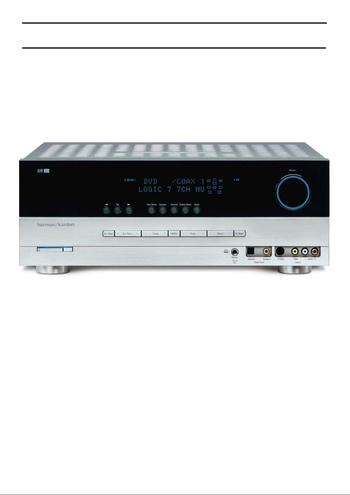
5 x 50W 7.1 CHANNEL A/V RECEIVER
CONTENTS
ESD WARNING………………………..…..2 ELECTRICAL PARTS LIST…….…..…12
BASIC SPECIFICATIONS........................3 SEMICONDUCTOR PINOUTS…....….54
TROUBLESHOOTING GUIDE.................4 PCB DRAW
PROCESSOR RESET..............................4 BLOCK DIAGRAM.............................119
PACKAGE LIST AND PARTS…...............5 WIRING DIAGRAM……………..….…120
DISASSEMBLY.........................................6 AMP BIAS ADJUSTMENT...…...…....121
UNIT EXPLODED VIEW AND PARTS…11 SCHEMATIC DIAGRAMS...………....122
Released EU2008 harman/kardon, Inc. Rev 0, 05/2008
250 Crossways Park Dr.
Woodbury, New York, 11797
INGS…………………..…110
Page 2
harman/kardon
AVR247/230 Service Manual
Page 2 of 131
Some semiconductor (solid state) devices can be damaged easily by static electricity. Such components commonly are called
Electrostatically Sensitive (ES) Devices. Examples of typical ES devices are integrated circuits and some field effect transistors and
semiconductor "chip" components.
The following techniques should be used to help reduce the incidence of component damage caused by static electricity.
1. Immediately before handling any semiconductor component or semiconductor-equipped assembly, drain off any electrostatic charge on
your body by touching a known earth ground. Alternatively, obtain and wear a commercially available discharging wrist strap device,
which should be removed for potential shock reasons prior to applying power to the unit under test.
2. After removing an electrical assembly equipped with ES devices, place the assembly on a conductive surface such as aluminum foil, to
prevent electrostatic charge build-up or exposure of the assembly.
3. Use only a grounded-tip soldering iron to solder or unsolder ES devices.
4. Use only an anti-static solder removal device. Some solder removal devices not classified as "anti-static" can generate electrical charges
sufficient to damage ES devices.
5. Do not use freon-propelled chemicals. These can generate electrical change sufficient to damage ES devices.
6. Do not remove a replacement ES device from its protective package until immediately before you are ready to install it. (Most replacement
ES devices are packaged with leads electrically shorted together by conductive foam, aluminum foil or comparable conductive material.)
7. Immediately before removing the protective material from the leads of a replacement ES device, touch the protective material to the
chassis or circuit assembly into which the device will be installed.
CAUTION :
8. Minimize bodily motions when handling unpackaged replacement ES devices. (Otherwise harmless motion such as the brushing together
or your clothes fabric or the lifting of your foot from a carpeted floor can generate static electricity sufficient to damage an ES devices.
Be sure no power is applied to the chassis or circuit, and observe all other safety precautions.
Each precaution in this manual should be followed during servicing.
Components identified with the IEC symbol in the parts list are special significance to safety. When replacing a component identified with
, use only the replacement parts designated, or parts with the same ratings or resistance, wattage, or voltage that are designated in the
parts list in this manual. Leakage-current or resistance measurements must be made to determine that exposed parts are acceptably
insulated from the supply circuit before retuming the product to the customer.
Page 3

Technical Specifications
harman/kardon
AVR247/230 Service Manual
Page 3 of 131
Audio Section
Stereo Mode
Continuous Average Power (FTC)
65 Watts per channel, 20Hz–20kHz,
@ < 0.07% THD, both channels driven into 8 ohms
7 Channel Surround Modes
Power Per Individual Channel
Front L&R channels:
50 Watts per channel,
@ < 0.07% THD, 20Hz–20kHz into 8 ohms
Center channel:
50 Watts, @ < 0.07% THD, 20Hz–20kHz into 8 ohms
Surround (L & R Side, Back) channels:
50 Watts per channel,
@ < 0.07% THD, 20Hz–20kHz into 8 ohms
Input Sensitivity/Impedance
Linear (High Level) 200mV/47kohms
Signal-to-Noise Ratio (IHF-A) 100dB
Surround System Adjacent Channel Separation
Analog Decoding 40dB
(Pro Logic, etc.)
Dolby Digital (AC-3) 55dB
DTS 55dB
Frequency Response
@ 1W (+0dB, –3dB) 10Hz–130kHz
High Instantaneous
Current Capability (HCC) ±35 Amps
Transient Intermodulation
Distortion (TIM) Unmeasurable
Rise Time 16 µsec
Slew Rate 40V/µsec**
FM Tuner Section
Frequency Range 87.5–108MHz
Usable Sensitivity IHF 1.3 µV/13.2dBf
Signal-to-Noise Ratio Mono/Stereo: 70/68dB (DIN)
Distortion Mono/Stereo: 0.2/0.3%
Stereo Separation 40dB @ 1kHz
Selectivity ±400kHz: 70dB
Image Rejection 80dB
IF Rejection 90dB
AM Tuner Section
Frequency Range 522–1620kHz
Signal-to-Noise Ratio 45dB
Usable Sensitivity Loop: 500µV
Distortion 1kHz, 50% Mod: 0.8%
Selectivity ±10kHz: 30dB
Video Section
Video Format PAL/NTSC
Input Level/Impedance 1Vp-p/75 ohms
Output Level/Impedance 1Vp-p/75 ohms
Video Frequency Response
(Composite and S-Video) 10Hz–8MHz (-3dB)
Video Frequency
Response (Component) 10Hz–100MHz (-3dB)
™
HDMI
Audio and video processing
General
Power Requirement AC 220–240V/50Hz
Power Consumption 65W idle, 540W maximum
(7 channels driven)
Dimensions (Max)
Width 440mm
Height 165mm
Depth 382mm
Weight 13.6 kg
This product incorporates copyright protection technology that is protected by method
claims of certain U.S.patents and other intellectual property rights owned by Macrovision
Corporation and other rights owners. Use of this copyright protection technology must be
authorized by Macrovision Corporation, and is intended for home and other limited viewing
uses only unless otherwise authorized by Macrovision Corporation. Reverse engineering or
disassembly is prohibited.
Depth measurement includes knobs, buttons and terminal connections.
Height measurement includes feet and chassis.
All features and specifications are subject to change without notice.
Harman Kardon, The Bridge and Logic 7 are registered trademarks of
Harman International Industries, Incorporated.
is a trademark of Harman International Industries, Inc.
*Manufactured under license from Dolby Laboratories.
“Dolby,”“Pro Logic” and the Double-D symbol are
trademarks of Dolby Laboratories.
"DTS","DTS ES","Neo:6"and"96/24" are trademarks of DTS,Inc.
SA-CD is a trademark of Sony Electronics, Inc.
Blu-ray Disc is a trademark of the Blu-ray Disc Association.
Apple and iPod are registered trademarks of Apple Computer, Inc.
Cirrus is a registered trademark of Cirrus Logic Corp.
**Without input anti slewing and output isolation networks.
Faroudja and DCDi by Faroudja are trademarks of Genesis Microchip, Inc.
HD-DVD is a trademark of the DVD Format/Logo Licensing Corporation (DVD FLLC).
HDMI, the HDMI logo and High-Definition Multimedia Interface are trademarks or
registered trademarks of HDMI Licensing, LLC.
Page 4

Troubleshooting Guide
harman/kardon
AVR247/230 Service Manual
Page 4 of 131
SYMPTOM CAUSE SOLUTION
Unit does not function when Main • No AC Power • Make certain AC power cord is plugged
Power Switch
Display lights, but no sound • Intermittent input connections • Make certain that all input and speaker
or picture connections are secure
No sound from any speaker; • Amplifier is in protection mode • Check speaker-wire connections for shorts at receiver
light around Power switch
No sound from surround or • Incorrect surround mode • Select a mode other than Stereo
center speakers • Input is mono • There is no surround information from mono sources (except with
Unit does not respond to • Weak batteries in remote • Change remote batteries
remote commands • Wrong device selected • Press the AVR Selector
1
is pushed into a live outlet
• Check to see if outlet is switch controlled
• Mute is on • Press Mute button
• Volume control is down • Turn up volume control
2
is red due to possible short and speaker ends
• Amplifier is in protection mode • Contact your local Harman Kardon service depot
due to internal problems
Theater and Hall surround modes)
• Incorrect configuration • Check speaker mode configuration
• Stereo or Mono program material • Some surround modes may not create rear-channel information
from nonencoded programs
• Remote sensor Úis obscured • Make certain front-panel sensor is visible to remote or
connect remote sensor
5
Intermittent buzzing in tuner • Local interference • Move unit or antenna away from computers, fluorescent lights,
motors or other electrical appliances
Letters flash in the Channel Indicator • Digital audio feed paused • Resume play for DVD
Display $and Digital Audio stops • Check that Digital Signal is fed to the Digital Input selected
Processor Reset
In the rare case where the unit’s operation or the
displays seem abnormal, the cause may involve
the erratic operation of the system’s memory or
microprocessor.
To correct this problem, first unplug the unit from
the AC wall outlet and wait at least three
minutes. After the pause,reconnect the AC
power cord and check the unit’s operation.If the
system still malfunctions, a system reset may
clear the problem.
To clear the AVR’s entire system memory
including tuner presets, output level settings,
delay times and speaker configuration data, first
put the unit in Standby by pressing the System
Power Control button
the Tone Mode button
The unit will turn on automatically. Note that
once you have cleared the memory in this manner,
it is necessary to re-establish all system
configuration settings and tuner presets.
2
. Next press and hold
8
for three seconds.
NOTE: Resetting the processor will erase any
configuration settings you have made for
speakers,output levels, surround modes, digital
input assignments as well as the tuner presets.
After a reset the unit will be returned to the
factory presets, and all settings for these items
must be reentered.
If the system is still operating incorrectly,there
may have been an electronic discharge or severe
AC line interference that has corrupted the
memory or microprocessor.
If these steps do not solve the problem, consult
an authorized Harman Kardon service depot.
Page 5
1. Instruction manual ass'y - Accessories
harman/kardon
AVR247/230 Service Manual
Page 5 of 131
2. Package Drawing
MICROPHONE ASS'Y
7
AVR247/230
1
5
9
POLY BAG
COVER ASS'Y
POLY BAG
2
AM LOOP ANTENNA ASS'Y
6
IMAGE BROCHURES
10
BOOKLET,INFORMATION
3
BATTERY ASS'Y
7
REMOCON ASS'Y
11
MANUAL INSTRUCTION
4
FM 1 POLE ANT
8
STAPLE
12
MANUAL SETUP GUIDE
2
SNOW PAD (L)
SET
4
ACCESSORY-1
1
SNOW PAD (R)
3
BOX ,OUT CARTON
5
13
STAPLE
NO DESCRIPTION PARTS NO. Q,ty
1
2
3
4
FM 1 POL ANT CSA1A018Z 1
5
COVER ASS'Y CGRAVR130/230ZA
COVER A
1
COVER B
2
SHEET,FRONT COVER
3
4
PAD , COVER
BAG , POLY
5
6 IMAGE BROCHURES HQE1A273Z 1
7
REMOCON ASS'Y CARTAVR247/230 1
8 STAPLE CPL0905 3
A
MICROPHONE ASS'Y
CPB1061WPOLY BAG
CSA1A027ZAM LOOP ANTENNA ASS'Y 1
CABR03P3BATTERY 3
CGR1A331M7H43 1
CQE1A220Z
CPS1A676 1
CPB1A176Z 1
ACCESSORY-2
ACCESSORY-2ACCESSORY-1
NO DESCRIPTION PARTS NO. Q,ty
1
1
1
1CGR1A332M7H43
1
9
BOOKLET,INFORMATION
10
11
MANUAL ,SETUP GUIDE
12
13
STAPLE CPL0905 3
A MICROPHONE ASS'T CJXAVR340MICRO 1
CQE1A180Z 1
CQX1A1255ZMANUAL,INSTRUCTION
CQX1A1256Z
1CPB1061WPOLY BAG
1
1
ACCESSORY-1
1
21SNOW,PAD(L)
3
SET AVR247/230SET 1
4
BOX,OUT CARTON
5
ACCESSORY-26 CQXAVR247/230 1
MICROPHONE ASS'Y7 CJXAVR340MICRO 1
DESCRIPTIONNO
CQXAVR247/230
CPS6A564
CPS6A565SNOW,PAD(R)
CPG1A822U
6
Q,tyPARTS NO.
1
1
1
Page 6
DISASSEMBLY
harman/kardon
AVR247/230 Service Manual
Page 6 of 131
AVR247/230
1. Removing the Top Cabinet
Remove the Screws
6
4
5
3. Removing the Rear Panel
13
1
~
10
9
11
7
8
12
13
3
1
2
Remove the Screws
10
11
12
13
14
15
16
25
26
9
7 6 5 4
8
27 29 30
33
1
~
21
22
23 24
28
31
18
17
1
3
2
32
33
19 20
9
8
4. Removing the Main PCB
1 7
Remove the Screws
~
2. Removing the Front Panel
Remove the Screws
7
6
5
1
4
2
3
1 9
~
1
5
2
6
3
4
7
Page 7

DISASSEMBLY PROCEDURES (AVR247)
harman/kardon
AVR247/230 Service Manual
Page 7 of 131
<1> TOP-CABINET(21) REMOVAL
1. Remove 13 screws(S1,S7) and then remove the Top-cabinet.
<2> FRONT PANEL ASS’Y REMOVAL
1. Remove the Top-cabinet, referring to the previous step<1>.
2. Disconnect the card cable between conn
and connector(CN72) on the Input PCB(39-1).
3. Disconnect the lead wire(BN81-8P) on the Fip PCB(37-1) from connector(CN81) on the Trans PCB(40-4).
4. Disconnect the lead wire(BN22-6P) on the Phone PCB(
5. Disconnect the lead wire(BN18-5P) on the Phone PCB(
6. Disconnect the lead wire(BN10-4P) on the Volume PCB(37-6) from conn
7. Disconnect the lead wire(BN41-6P) on the Volume PCB(37-6) from conn
8. Disconnect the lead wire(BN90-2P) on the Main PCB(38
9. Remove 1 screw(S10) and then lead wire(JW82-1P,JW83-1P) on the Phone PCB(37-5).
10 .Remove 1screw(S10) and then lead wire(JW84-1P) on the Volume PCB(37-3).
11. Remove 10 scre ws(S1) and then remov e the Front Panel ASS’Y.
<3> Volume PCB(37-6) REMOVAL
1. Remove the Top-cabinet, referring to the previous step<1>.
2. Remove the Front Panel ASS’Y, referring to the previous step<2>.
3. Pull out the Volume Knob ASS’Y.
4. Disconnect connector(CN84) on the Volume PCB(37-6) from the lead
5. Disconnect the lead wire(BN92-5P)on the Volume PCB(
6. Remove 8 screws(S2,S14), and then remove the Volume PCB(37-6).
<4>PHONE PCB(37-5) REMOVAL
1. Remove the Top-cabinet, referring to the previous step<1>.
2. Remove the Front Panel ASS’Y, referring to the previous step<2>.
3. Disconnect connector(CN92) on the Phone PCB(37-5) from the lead wire(BN92-5P) on the Volume PCB(37-6).
4.. Disconnect connector(CN85)on the Phone PCB(37-5) from the lead wire(BN85-3P) on the Fip PCB(37-1).
5. Remove 2 screws(S2) and then remove the Phone PCB(37-5).
<5>POWER LED PCB(37-3) REMOVAL
1. Remove the Top-cabinet, referring to the previous step<1>.
2. Remove the Front Panel ASS’Y, referring to the previous step<2>.
3. Disconnect connector(CN88) on the Power Led PCB(37-3) from the lea
4. Remove 2 screws(S2) and then remove the Power led PCB(37-3).
<6>FIP PCB(37-1) REMOVAL
1. Remove the Top-cabinet, referring to the previous step<1>.
2. Remove the Front Panel ASS’Y, referring to the previous step<2>.
3. Disconnect the lead wire(BN84-5P) on the Fip PCB(3
4. Disconnect the lead wire(BN85-3P) on the Fip PCB(37
5. Disconnect the lead wire(BN88-4P) on the Fip PCB(37
ector(CN72-17p) on the Fip PCB(37-1)
37-5) from connector(CN22) on the Input PCB(39-1).
37-5) from connector(CN18) on the Input PCB(39-1).
ector(CN10) on the Input PCB(39-1).
ector(CN41) on the Video PCB(41).
-1) from connector(CN86) on the Moms PCB(37-4).
ire(BN84-5P) on the Fip PCB(37-1).
w
37-6) from connector(CN92) on the Phone PCB(37-5).
wire(BN88-4P) on the Fip PCB(37-1) .
d
-1) from connector(CN84) on the Volume PCB(37-6).
7
-1) from connector(CN85) on the Phone PCB(37-5).
-1) from connector(CN88) on the Power Led PCB(37-3).
Page 8

6. Disconnect the connector (CN89) on the Fip PCB(37-1) from lead wire(BN89-4P) on the Key PCB(37-2).
harman/kardon
AVR247/230 Service Manual
Page 8 of 131
7. Remove 3 screws(S2) and then remove the Guide PCB(37-8) & the Fip PCB(37-1).
<7>KEY PCB(37-2) REMOVAL
1. Remove the Top-cabinet, referring to the previous step<1>.
2. Remove the Front Panel ASS’Y, referring to the previous step<2>.
3. Remove the Fip PCB(37-1), referring to the previous step<6>.
4. Remove 10 screws(S2) and then remove the Key PCB(37-2).
<8>TUNER MODULE(44) REMOVAL
1. Remove the Top-cabinet, referring to the previous step<1>.
2. Disconnect the card cable between conne
ctor(CON1-1
3P) on the Tuner module(44)
and connector(CN13) on the Input PCB(39-1).
3. Remove 2 screws(S8) and then remove the Tuner Module(44).
<9>HUDSON PCB(42) REMOVAL
1. Remove the Top-cabinet, referring to the previous step<1>.
2. Disconnect connector(CN80) on the HUDSON PCB(42) from the lead
ire(BN80-3P) on the RS232 PCB(37-7).
w
3. Remove 3 screws(S15).
4. Disconnect the board to board connector between and connector(CN81-44P) on the HUDSON PCB(42)
and connector(BN81-44P) on VIDEO PCB(41) and then r
emove the HUDSON PCB(42).
<10>VIDEO PCB(41) REMOVAL
1. Remove the Top-cabinet, referring to the previous step<1>.
2. Remove the Hudson PCB(42), referring to
3. Disconnect the card cable between conn
the previ
ector(BN14-17p) on the Video PCB(41)
ous step<9>.
and connector(CN14) on the Input PCB(39-1).
4. Disconnect connector(CN43) on the Video PCB(41)
from the lead wire(BN43-3P) on the Regul
5. Disconnect connector(CN41) on the Video PCB(41) from
the lead wire(BN41-6P) on the Volume PCB(37-6).
ator PCB(A)(40-2).
6. Disconnect the card cable between connector(CN42) on the Video PCB(41)
and connector(BN44-7P) on the iPod PCB(39-2).
7. Disconnect the card cable between connector(BN15-15P) on the Video PCB(41)
and connector(CN15-15P) on the INPUT PCB(39-1).
8. Remove 6 screws(S8) and then remove the Video PCB(41).
<11>iPod PCB(39-2) REMOVAL
1. Remove the Top-cabinet, referring to the previous step<1>.
2. Remove the Hudson PCB(42), referring to
the previ
ous step<9>.
3. Remove the Video PCB(41), referring to the previous step<10>
4. Disconnect the card cable between connector(BN19-15P) on the the iPod PCB(39-2)
and connector(CN19) on the Input PCB(39-1).
5. Disconnect the card cable between conne
ctor(BN44-
7P) on the iPod PCB(39-2)
and connector(CN42) on the Video PCB(41).
6. Disconnect the card cable between connector(CN47-7P) on the iPod PCB(39-2)
and connector(CN47) on the RS232 PCB(37-7).
7. Disconnect the board to board connector betw
en and connector(CN23) on the XM PCB(39-4)
e
and connector(BN17-12P) on the iPod PCB(39-2).
Page 9

8. Remove 2 screws(S13) and then remove the iPod PCB(39-2).
harman/kardon
AVR247/230 Service Manual
Page 9 of 131
<12>XM PCB(39-4) REMOVAL
1. Remove the Top-cabinet, referring to the previous step<1>.
2. Remove the Hudson PCB(42), referring to the previ
ous step<9>.
3. Remove the Video PCB(41), referring to the previous step<10>
4. Disconnect the card cable between connector(BN21-7P) on XM PCB(39-4)
and connector(CN21) on the input PCB(39-1).
5. Disconnect the lead wire(BN85-2P) on the XM PCB(39-4) from connector(CN85) on the Regulator PCB(A)(40-2).
6. Disconnect the board to board connector betwe
en and connector(CN23) on the XM PCB(39-4)
and connector(BN17-12P) on the iPod PCB(39-2).
7. Remove 1 screws(S15) and then remove the XM PCB(39-4).
<13>RS232 PCB(37-7) REMOVAL
1. Remove the Top-cabinet, referring to the previous step<1>.
2. Remove the Hudson PCB(42), referring to
the previ
ous step<9>.
3. Remove the Video PCB(41), referring to the previous step<10>.
4. Disconnect the card cable between conne
ctor(CN47-
7P) on the iPod PCB(39-2)
and connector(CN47) on the RS232 PCB(37-7).
5.Remove 2 screws and then remove the RS232 PCB(37-7).
<14>INPUT PCB(39-1) REMOVAL
1. Remove the Top-cabinet, referring to the previous step<1>.
2. Remove the Tuner module(44), referring to the previous step<8>.
3. Remove the Hudson PCB(42), referring to the previ
ous step<9>.
4. Remove the Video PCB(41), referring to the previous step<10>.
5. Disconnect connector(CN20) on the the Input PCB(39-1)
from the lead wire(BN20-5P) on the Regul
6. Disconnect connector(CN22) on the Input PCB(39-1) from the lead w
7. Disconnect connector(CN18) on the Input PCB(39-1) from the lead w
8. Disconnect connector(CN10) on the Input PCB(39-1) from the lead w
9. Disconnect the card cable between connector(CN14) on the
ator PCB(B)(40-5).
ire(BN22-6P) on the Phone PCB(37-5).
ire(BN18-5P) on the Phone PCB(37-5)
ire(BN10-4P) on the Volume PCB(37-6).
Input PCB(39-1).
and connector(BN14-17P) on the Video PCB(41).
10. Disconnect the card cable between connector(CN19) on the Input PCB(39-1)
and connector(BN19-15P) on the I-Pod PCB(39-2).
11. Disconnect the card cab le between connector(CN21) on the input PCB(39-1)
and connector(BN21-7P) on XM PCB(43).
12. Disconnect the card cable between connector(CN12-21p) on the Input PCB(39-1)
and connector(CN12-21p)) on the main PCB(38-1)
13. Disconnect the card cable between connector(CN11-17p) on the Input PCB(39-1)
and connector(CN11) on the main PCB(38-1)
14. Disconnect the card cable between con
n
ector(CN72) on the Input PCB(39-1)
and connector(CN72-17p) on the Fip PCB(37-1)
15. Remove 11 screws(S8,S15) and then remove the Inp ut PCB(39-1).
<15>POWER TRANS(36) & POWER PCB ASS’Y(40) REMOVAL
1. Remove the Top-cabinet, referring to the previous step<1>.
2. Disconnect lead wire of the Power Trans(36) from connector (CN91-3P) on the Main PCB(38-1)
3. Disconnect connector(CN19-3P,CN20-4P) on TRANS PCB(40-3)
Page 10

from the lead wire(BN19-3P,BN20-4P) on the Main PCB(38-1).
harman/kardon
AVR247/230 Service Manual
Page 10 of 131
4. Disconnect the lead wire(BN96-8P) on the Power PCB(40-4)
from connector(CN96) on the Regulator PCB(B)(40-5).
5. Disconnect the lead wire(BN99-8P) on the Power PCB(40-4)
from connector(CN99) on the Regulator PCB(A)(40-2).
6. Disconnect connector(CN81) on the Trans PCB(40-4) from the lead
wire(BN81-8P) on the Fip PCB(37-1).
7. Remove 4 Trans screws(S9) and then remove the Power Trans(36)& Power PCB ASS’Y(40) REMOVAL .
<16>REMOTE PCB ASS’Y(40-7) REMOVAL
1. Remove the Top-cabinet, referring to the previous step<1>.
2.Disconnect connector(CN88) on the remote PCB(40-7) from
the lead wire(BN88-6P) on the Main PCB(38-1)
3. Remove 3screws(S13) and then remove the Remote PCB ASS’Y(40-7).
<17>MAIN PCB ASS’Y(38-1) REMOVAL
1. Remove the Top-cabinet, referring to the previous step<1>.
2. Remove the Tuner module(44), referring to the previous step<8>.
3. Remove the Hudson PCB(42), referring to
the previ
ous step<9>.
4. Remove the Video PCB(41), referring to the previous step<10>.
5. Remove the iPod PCB(39-2), referring to the previous step<11>.
6. Remove the XM PCB(39-4), referring to the previous step<12>.
7. Remove the RS232 PCB(37-7), referring to the previous step<13>.
8. Remove the Input PCB(39-1), referring to the previ
ous step<14>.
9. Remove the AC Cord(35) on the Main PCB(38-1)
10. Disconnect the lead wire(BN90-2P) on the Main PCB(38-1) from connector(CN86) on Moms PCB(37-4).
11. Disconnect conn ector (CN91-3P) on the Main PCB(38-
1) from lead wire of the Power Trans(36)
12. Disconnect the lead wire(BN89-2P) on the Main PCB(38-1)
from connector(CN89) on Regulator PCB(A)(40-2).
13. Disconnect the lead wire(BN19-3P,BN20-4P) on the Main PCB(38-1)
from connector(CN19-3P,CN20-4P) on TRANS PCB(40-4).
14. Disconnect the lead wire(BN88-6P) on the Main PCB(38
15. Disconnect the lead wire of the DC, FAN(49) from connector(CN
16. Remove 11screws(S13-1EA, S4-2EA, S6-2EA, S8-6EA) and then
-1) from connector(CN88) on remote PCB(40-7).
89-2P) on the Main PCB(38-1).
remove the Main PCB ASS’Y(38-1).
Page 11
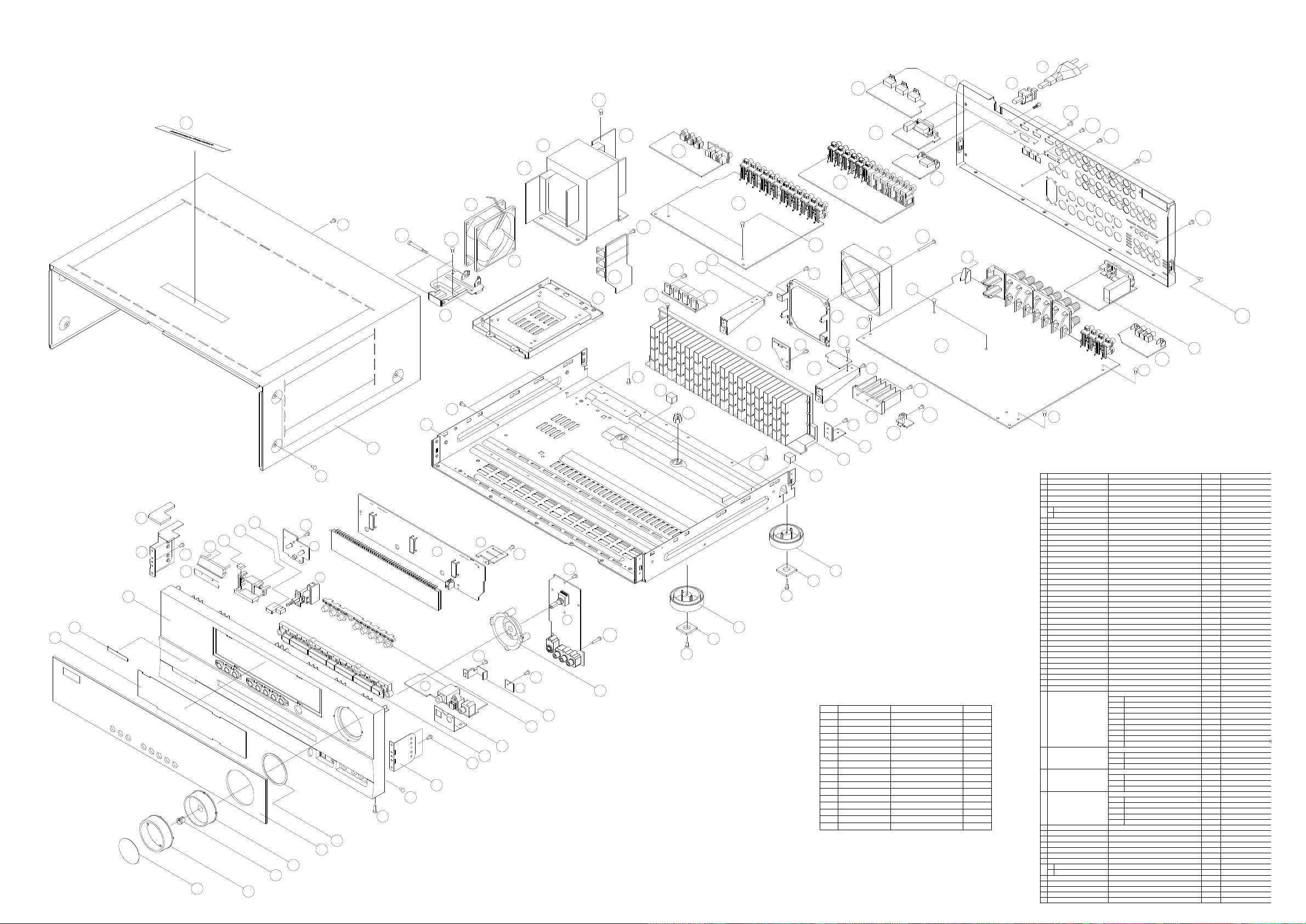
AVR247/230 EXPLODED VIEW
harman/kardon
AVR247/230 Service Manual
Page 11 of 131
35
42
33
S9
47
36
40-1
40-3
37-7
40-4
41
39-2
34
S15
S13
S13
S8
S5
40-2
23
39-1
24
38-2
S10
S13
S15
48
S16
32
S5
S6
x2
18
S4
39-5
S4
S5
38-1
43
40-7
S4
S4
S10
S12
30
51
S5
40-2
S14
S4
27
26
REMARK
DESCRIPTION
25
24
23
S4
DESCRIPTION PARTS NO. Q,ty
NO
S1
SCREW
S2
S3
SCREW
S4
SCREW
S5
SCREW
S6
SCREW
S7
SCREW
S8
SCREW,TRANS
S9
SCREW
S10
SCREW
S11
SCREW
S12
SCREW
S13
SCREW,SPECIAL CHD1A012R 21
S14
SCREW,SPECIAL CHD1A012ZR 2
S15
SCREW,SPECIAL CHD3A012R 7
S16
SCREW,SPECIAL CHD4A012R 5
S17
CTB3+10GR
CTW3+8JR
CTB3+8JR
CTW3+12JR
CTB4+6FFC
CTB3+10GFZR
CHD1A023R
CTB3+6JR
CTB3+16GFZR
CTB3+10JRR
CTB3+8FFZR
13CTB3+8JFCSCREW
31
9
10
3
6
22
4
19
2
3
8
NO
ORNAMENT,VOLUME CGU1A318Z 1
1
CAP,VOLUME
2
HOLDER,VOLUME
3
INDICATOR,VOLUME
4
WINDOW ASS'Y
5
WINDOW,FIP CGU1A399Y
1
BADGE,MODEL
2
6
FILTER,FIP
7
BDAGE,HARMAN/KARDON
8
PANEL,FRONT
9
BRACKET,SIDE
10
KNOB,FUNCTION
11
KNOB,DISPLAY
12
KNOB,POWER
13
INDICATOR,POWER
14
KNOB,MOMS
15
BRACKET,PCB CMK2A010
16
PLATE,SHIELD
17
BRACKET , FAN CMD1A600 1
18
HOLDER,LED
19
BRACKET,FIP
20
CABINET,TOP
21
CHASSIS,BOTTOM
22
RUBBER,CUSHION
23
FOOT
24
SUPPORT,CUSHION
25
HEAT SINK
26
BRACKET,PCB
27
HOLDER,PCB
28
BRACKET,TRANS
29
BRACKET,PCB(H/T)
30
BRACKET,PCB CMD1A570 1
31
BRACKET,PCB
32
PANEL,REAR
33
BUSHING,AC CORD
34
CORD,POWER
35
TRANS,POWER
36
FRONT PAB ASS'Y
37
MAIN PCB ASS'Y COP11911O 1
38
INPUT PCB ASS'Y COP11913O 1
39
POWER PCB ASS'Y
40
VIDEO PCB ASS'Y
41
HUDSON PCB ASS'Y COP11915O 1
42
TUNER MODULE
43
44
RUBBER
45
46
BADGE ASS'Y
47
ORNAMENT,BADGE
1
BADGE,H/K(TOP)
2
FAN(80*80*25mm)
48
BEACKET,FAN(A) CMD1A615 1
49
SHEET,REFLECTION CMZ1A120 1
50
HEAT SINK CMY2A249 1
51
PARTS NO.
CGX1A338MBC63
CMH1A214
CGL1A222
CGUAVR247
CGB1A179Z
CMZ2A090SHEET,VOLUME 1
CMZ1A088
KGB1A158Z
CGW1A427RDNH43
CMD2A443
CBT1A1028MBYG27
CBT1A1027K128
CBT1A1026MMZG27
CGL1A258Z
CBC1A158MBZG27
CMC1A302
CMH1A215
CMD1A209
CKC5B145S46Z
CUA3A229
CHG1A329
CKL2A069H43
CHG1A104Z
CMY1A271
CMD1A417
CHE1A170
CMD2A487
CMD1A398
CMD1A387
CKF12A319Z
KHR1A028
CJA2B043ZA
CLT5W026ZE
COP11910O
FIP PCB
37-1
KEY PCB
37-2
POWER LED PCB
37-3
MOMS PCB
37-4
PHONE PCB
37-5
VOLUME PCB
37-6
RS232 PCB
37-7
GUIDE PCB(CARD CABLE)
37-8
MAIN PCB
38-1
GUIDE PCB(CARD CABLE) 1
38-2
INPUT PCB
39-1
ipod PCB 1
39-2
RDS PCB 1
39-5
COP11916O 1
VIDEO PCB 1
40-1
REGULATOR PAC(A) 7
40-2
TRANS PCB 1
40-3
TRANS PCB 1
40-4
REGULATOR PCB(B) 1
40-5
COP11918O 1
CNVM9014MS171L
CHG1A309
CHG1A160ZCUSHION 1
CGX1A375ZA
CGX1A375M7G32
KGB1A159Z
CFNCF12825MS
Q,ty
1
1
1
1
1
1
1
1
1
1
11
1
1
1
1
1
1
1
3
1
1
4
4
1
1
2
2
1
2
2
1
1
1
1
1
1
1
1
1
1
1
1
1
1
1
1
1
1
1CMD1A555BRACKET,SIDE(L)
1
1
1
1
2
48
S1
S16
S9
47
29
40-5
S16
S17
S16
30
49
S5
46
S5
28
22
21
S7
45
44
14
S2
50
14-1
15
13
S2
37-3
37-1
37-4
37-8
S2
S2
9
8
7
S2
37-5
37-9
37-6
S11
S4
S2
19
16
12
17
11
S2
10
S1
S1
6
5
4
3
1
2
Page 12

AVR247/230 Electrical Parts List
harman/kardon
AVR247/230 Service Manual
Page 12 of 131
Ref. # Part Number
CGL1A222 INDICATOR , VOLUME INDICATOR 1
CGUAVR247/230 WINDOW ASS'Y ASS'Y 1
CGB1A179Z BADGE, HARMAN(AVR247/230) BADGE 1
CGU1A399Y WINDOW , FIP FIP WINDOW 1
CGU1A318Z ORNAMENT , VOLUME ORANMENT 1
CGX1A338MBC63 CAP , VOLUME CAP 1
CGX1A375ZA BADGE ASS'Y ASS'Y 1
CHE36-3 CLAMPER , WIRE CLAMPER 1
CKC5B145S46Z CABINET , TOP TOP CABINEET 1
BKC5C145S46 CABINET , TOP TOP CABINEET 1
CLZ9Z028Z FERRITE CORE(21.2X6.4X12.7) FERRITE CORE 3
CMH1A214 HOLDER , VOLUME HOLDER 1
CMZ2A090 SHEET , VOLUME SHEET 1
CQB1A549Y LABEL , ATTENTION DVD48 LABEL 1
CQB1A551Z LABEL , BAR CODE LABEL 1
CQB1A622 LABEL , SERIAL NO LABEL 1
CQB1A797Z LABEL , HDMI LABEL 2
CTB3+8JFC SCREW SCREW 13
CTB4+6FFC SCREW SCREW 6
CHE154 CLAMPER , ARM CLAMPER 0,12
CJXAVR340MICRO MICRO PHONE ASS'Y ASS'Y 1
CPG1A822U BOX , OFFSET CARTON BOX 1
CPP1A081Z BAG,POLY SET BAG 1
CPS6A564 PAD , SNOW L SNOW PAD 1
CPS6A565 PAD , SNOW R SNOW PAD 1
CQB1A551Z LABEL , BAR CODE LABEL 2
CQB1A795Z LABEL , COUNTRY AVR245/230 LABEL 2
CQS1A001 RIBON , BAR CODE SONY(TR-4070) 0,12
CQXAVR247/230 INSTRUCTION MANUAL ASS'Y ASS'Y 1
CABR03P3 BATTERY (SIZE 'AAA') 3PCS IN 1 BATTERY 3
CARTAVR247/230 REMOCON TRANSMITTER ASS'Y ASS'Y 1
CGRAVR130/230ZA COVER ASS'Y ASS'Y 1
CGR1A331M7H43 COVER A COVER 1
CGR1A332M7H43 COVER B COVER 1
CPS1A676 PAD , COVER PAD 1
CQE1A220Z SHEET , FRONT COVER SHEET 1
CQE1A180Z BOOKLET , IMFORMATIONS BOOKLET 1
CQX1A1255Z MANUAL , INSTRUCTION AVR247/230 SHEET 1
CQX1A1256Z MANUAL , SET UP AVR147/230 MANUAL 1
CSA1A018Z FM 1 POLE ANT ANT 1
CSA1A027Z AM LOOP ANT ANT 1
HQE1A273Z HARMAN IMAGE BROCHURES BROCHURES 1
CRE1A037 LOCKER LOCKER 14
Description
Value Qty
FRONT PANEL ASSY
Ref. # Part Number
Description
Value Qty
CGWAVR247/230 FRONT PANEL ASS'Y ASS'Y 1
CBC1A158MBZG27 KNOB , MOMS KNOB 1
CBT1A1026MMZG27 KNOB , POWER KNOB 1
CBT1A1027K128 KNOB , DISPLAY KNOB 1
CBT1A1028MBYG27 KNOB , FUNCTION KNOB 1
CGL1A258Z INDICATOR , POWER INDICATOR 1
CGW1A427RDNH43 PANEL , FRONT AVR247/230 PANEL 1
CHG1A309 RUBBER RUBBER 1
CHR301 CLAMPER CLAMPER 20
CLZ9Z028Z FERRITE CORE(21.2X6.4X12.7) FERRITE CORE 4
CMC1A302 PLATE , SHIELD PLATE 1
Page 13

FRONT PANEL ASSY
harman/kardon
AVR247/230 Service Manual
Page 13 of 131
Ref. # Part Number
CMD1A555 BRACKET , SIDE (L) BRACKET 1
CMD2A443 BRACKET , SIDE BRACKET 1
CMH2A215 HOLDER , LED AVR350 HOLDER 1
CMK2A010 BRACKET , PCB BRACKET 1
CMZ1A088 FILTER , FIP FIP FILTER 1
CMZ1A120 SHEET , REFLECTION SHEET 1
CTB3+10GR SCREW SCREW 31
CTB3+16GFZR SCREW SCREW 2
KGB1A158Z BADGE , HARMAN/KARDON(FRONT) BADGE 1
CB72 CWCAVR350CN72 CABLE , SHIELD CARD(17PIN, 240MM) CARD CABLE(SHILED) 1
Description
Value Qty
FRONT PCB ASSY
Ref. # Part Number
COP11910O AVR247/230 FRONT PCB ASS'Y ASS'Y 1
CMC3A111 PLATE , EARTH PLATE 1
CMD1A618 BRACKET , RESET BRACKET 1
C402 CCEA1HH100T CAP , ELECT 10UF 50V 1
C403 CCEA1HH100T CAP , ELECT 10UF 50V 1
C714 HCBS1H151KBT CAP , CERAMIC 150UF 50V K 1
C716 CCEA1AH331T CAP , ELECT 330UF 10V 1
C719 HCBS1H102KBT CAP , CERAMIC 1000PF 50V K 1
C720 HCBS1H102KBT CAP , CERAMIC 1000PF 50V K 1
C721 HCBS1H102KBT CAP , CERAMIC 1000PF 50V K 1
C723 HCBS1H104ZFT CAP , CERAMIC 0.1UF 50V Z 1
C728 HCBS1H104ZFT CAP , CERAMIC 0.1UF 50V Z 1
C729 HCBS1H473ZFT CAP , CERAMIC 0.047UF 50V Z 1
C731 CCEA1HH100T CAP , ELECT 10UF 50V 1
C735 CCEA1CKS100T CAP , ELECT 10UF 16V 1
C742 HCBS1H223ZFT CAP , CERAMIC 0.02UF 50V Z 1
C793 HCBS1H104ZFT CAP , CERAMIC 0.1UF 50V Z 1
C794 HCBS1C222MXT CAP , CERAMIC 2200PF 16V 1
C795 HCBS1H102KBT CAP , CERAMIC 1000PF 50V K 1
C796 HCBS1H102KBT CAP , CERAMIC 1000PF 50V K 1
C805 HCBS1H223ZFT CAP , CERAMIC 0.022UF 50V Z 1
C806 HCBS1H223ZFT CAP , CERAMIC 0.022UF 50V Z 1
C807 HCBS1H104ZFT CAP , CERAMIC 0.1UF 50V Z 1
C808 HCBS1H181KBT CAP , CERAMIC 180PF 50V 1
C809 CCEA1AH471T CAP , ELECT 470PF 10V 1
C812 HCBS1H104ZFT CAP , CERAMIC 0.1UF 50V Z 1
C817 HCBS1H100JCT CAP , CERAMIC 10PF 50V 1
C820 CCEA1HH100T CAP , ELECT 10UF 50V 1
C821 CCEA1EH470T CAP , ELECT 47UF 25V 1
C822 CCEA1EH470T CAP , ELECT 47UF 25V 1
C823 CCEA1HH100T CAP , ELECT 10UF 50V 1
C824 HCBS1H471KBT CAP , CERAMIC 470PF 50V 1
C825 HCBS1H151KBT CAP , CERAMIC 150PF 50V 1
C828 HCBS1H470JT CAP , CERAMIC 47PF 50V 1
C830 HCBS1H473ZFT CAP , CERAMIC 0.047F 50V 1
C841 CCEA1HH100T CAP , ELECT 10UF 50V 1
C842 CCEA1HH100T CAP , ELECT 10UF 50V 1
C843 CCEA1HH100T CAP , ELECT 10UF 50V 1
C850 HCBS1H471KBT CAP , CERAMIC 470PF 50V 1
C851 HCBS1H471KBT CAP , CERAMIC 470PF 50V 1
C852 HCBS1H104ZFT CAP , CERAMIC 0.1UF 50V Z 1
C855 HCBS1H101KBT CAP , CERAMIC 100PF 50V K 1
C856 HCBS1H101KBT CAP , CERAMIC 100PF 50V K 1
C857 HCBS1H104ZFT CAP , CERAMIC 0.1UF 50V Z 1
C862 HCBS1H101KBT CAP , CERAMIC 100PF 50V K 1
Description
Value Qty
Page 14

FRONT PCB ASSY
harman/kardon
AVR247/230 Service Manual
Page 14 of 131
Ref. # Part Number
C863 HCBS1H101KBT CAP , CERAMIC 100PF 50V K 1
C866 CCEA1HKS100T CAP , ELECT 10UF 50V SMALL SIZE 1
C867 CCEA1HKS100T CAP , ELECT 10UF 50V SMALL SIZE 1
C868 CCEA1EKS470T CAP , ELECT 47UF 25V 1
C869 CCEA1EKS470T CAP , ELECT 47UF 25V 1
C870 HCBS1H681KBT CAP , CERAMIC 680PF 50V K 1
C871 HCBS1H681KBT CAP , CERAMIC 680PF 50V K 1
C872 CCEA1CH331T CAP , ELECT 330UF 16V 1
C873 CCEA1CH331T CAP , ELECT 330UF 16V 1
C874 HCBS1H101KBT CAP , CERAMIC 100PF 50V K 1
C882 HCBS1H104ZFT CAP , CERAMIC 0.1UF 50V Z 1
C889 HCBS1H104ZFT CAP , CERAMIC 0.1UF 50V Z 1
C891 HCBS1H223ZFT CAP , CERAMIC 0.023UF 50V Z 1
C892 HCBS1H223ZFT CAP , CERAMIC 0.023UF 50V Z 1
C893 HCBS1H223ZFT CAP , CERAMIC 0.023UF 50V Z 1
C894 CCEA1CKS100T CAP , ELECT 10UF 16V 1
C896 HCBS1H223ZFT CAP , CERAMIC 0.023UF 50V Z 1
C897 CCEA1AH471T CAP , ELECT 470UF 10V 1
C901 HCBS1H390JT CAP , CERAMIC 39PF 50V Z 1
C903 CCEA1HKS2R2T CAP , ELECT 2.2UF 50V 1
C905 CCEA1HKS2R2T CAP , ELECT 2.2UF 50V 1
C953 HCBS1H104ZFT CAP , CERAMIC 0.1UF 50V Z 1
C954 HCBS1H104ZFT CAP , CERAMIC 0.1UF 50V Z 1
C957 HCBS1H104ZFT CAP , CERAMIC 0.1UF 50V Z 1
D455 CVD1SS133MT DIODE 1SS133 1
D730 CVD1SS133MT DIODE 1SS133 1
D774 CVD1SS133MT DIODE 1SS133 1
D778 HVD1N5819T DIODE , SCHOTTKY 1N5819 1
D784 CVD1SS133MT DIODE 1SS133 1
D785 CVD1SS133MT DIODE 1SS133 1
J906 CRD20TJ391T RES , CARBON 390OHM 1/5W 1
L702 HLQ02C100KT COIL , AXAIL 10uH 1
Q401 HVTKRC104MT T.R KRC104M 1
Q451 HVTKRC107MT T.R KRC107M 1
Q452 HVTKRA107MT T.R KRA107M 1
Q454 HVTKRC107MT T.R KRC107M 1
Q701 HVTKRC107MT T.R KRC107M 1
Q722 HVTKRA107MT T.R KRA107M 1
Q724 HVTKRC107MT T.R KRC107M 1
Q725 HVTKRC107MT T.R KRC107M 1
Q734 HVTKTC2874BT T.R , MUTE KTC2874B 1
Q735 HVTKTC2874BT T.R , MUTE KTC2874B 1
Q736 HVTKTC2874BT T.R , MUTE KTC2874B 1
Q737 HVTKTC2874BT T.R , MUTE KTC2874B 1
Q738 HVTKRC107MT T.R KRC107M 1
Q739 HVTKTA1271YT T.R KTA1271Y 1
R402 CRD20TJ101T RES , CARBON 100 OHM 1/5W J 1
R403 CRD20TJ104T RES , CARBON 100K OHM 1/5W J 1
R404 CRD20TJ101T RES , CARBON 100 OHM 1/5W J 1
R452 CRD20TJ103T RES , CARBON 10K OHM 1/5W J 1
R453 CRD20TJ362T RES , CARBON 3.6K OHM 1/5W J 1
R454 CRD20TJ102T RES , CARBON 1K OHM 1/5W J 1
R701 CRD20TJ103T RES , CARBON 10K OHM 1/5W J 1
R704 CRD20TJ100T RES , CARBON 10 OHM 1/5W J 1
R705 CRD20TJ820T RES , CARBON 82 OHM 1/5W J 1
R706 CRD20TJ820T RES , CARBON 82 OHM 1/5W J 1
R708 CRD20TJ820T RES , CARBON 82 OHM 1/5W J 1
R709 CRD20TJ470T RES , CARBON 47 OHM 1/5W J 1
R710 CRD20TJ470T RES , CARBON 47 OHM 1/5W J 1
Description
Value Qty
Page 15

FRONT PCB ASSY
harman/kardon
AVR247/230 Service Manual
Page 15 of 131
Ref. # Part Number
R711 CRD20TJ470T RES , CARBON 47 OHM 1/5W J 1
R718 CRD20TJ222T RES , CARBON 2.2K OHM 1/5W J 1
R737 CRD20TJ100T RES , CARBON 10 OHM 1/5W J 1
R747 CRD20TJ103T RES , CARBON 10K OHM 1/5W J 1
R753 CRD20TF1001T RES , CARBON 1K /1/5W /F 1
R754 CRD20TF1501T RES , CARBON 1.5K /1/5W /F 1
R755 CRD20TF1801T RES , CARBON 1.8K /1/5W /F 1
R756 CRD20TF2701T RES , CARBON 2.7K /1/5W/F 1
R757 CRD20TF3301T RES , CARBON 3.3K /1/5W/F 1
R758 CRD20TF5601T RES , CARBON(5.6K/F) 5.6K 1/5W F 1
R759 CRD20TF1001T RES , CARBON 1K /1/5W /F 1
R760 CRD20TF1501T RES , CARBON 1.5K /1/5W /F 1
R761 CRD20TF1801T RES , CARBON 1.8K /1/5W /F 1
R762 CRD20TF2701T RES , CARBON 2.7K /1/5W/F 1
R763 CRD20TF3301T RES , CARBON 3.3K /1/5W/F 1
R764 CRD20TF5601T RES , CARBON(5.6K/F) 5.6K/1/5W/F 1
R765 CRD20TF7501T RES , CARBON (7.5K/F) 7.5K/1/5W/F 1
R766 CRD20TF1001T RES , CARBON 1K /1/5W /F 1
R767 CRD20TF1501T RES , CARBON 1.5K /1/5W /F 1
R768 CRD20TF1801T RES , CARBON 1.8K /1/5W /F 1
R769 CRD20TF2701T RES , CARBON 2.7K /1/5W/F 1
R781 CRD20TJ102T RES , CARBON 1K OHM 1/5W J 1
R782 CRD20TJ103T RES , CARBON 10K OHM 1/5W J 1
R783 CRD20TJ102T RES , CARBON 1K OHM 1/5W J 1
R784 CRD20TJ102T RES , CARBON 1K OHM 1/5W J 1
R786 CRD20TJ152T RES , CARBON 1.5K OHM 1/5W J 1
R787 CRD20TJ101T RES , CARBON 100 OHM 1/5W J 1
R791 CRD20TJ822T RES , CARBON 8.2K OHM 1/5W J 1
R805 CRD20TJ104T RES , CARBON 100K OHM 1/5W J 1
R806 CRD20TJ472T RES , CARBON 4.7K OHM 1/5W J 1
R824 CRD20TJ221T RES , CARBON 220 OHM 1/5W J 1
R825 CRD20TJ681T RES , CARBON 680 OHM 1/5W J 1
R828 CRD20TJ221T RES , CARBON 220 OHM 1/5W J 1
R829 CRD20TJ681T RES , CARBON 680 OHM 1/5W J 1
R864 CRD20TJ272T RES , CARBON 2.7K OHM 1/5W J 1
R865 CRD20TJ101T RES , CARBON 100 OHM 1/5W J 1
R866 CRD20TJ272T RES , CARBON 2.7K OHM 1/5W J 1
R869 CRD20TJ750T RES , CARBON 75 OHM 1/5W J 1
R871 CRD20TJ104T RES , CARBON 100K OHM 1/5W J 1
R872 CRD20TJ104T RES , CARBON 100K OHM 1/5W J 1
R873 CRD20TJ471T RES , CARBON 470 OHM 1/5W J 1
R874 CRD20TJ471T RES , CARBON 470 OHM 1/5W J 1
R875 CRD20TJ103T RES , CARBON 10K OHM 1/5W J 1
R876 CRD20TJ750T RES , CARBON 75 OHM 1/5W J 1
R877 CRD20TJ750T RES , CARBON 75 OHM 1/5W J 1
R878 CRD20TJ750T RES , CARBON 75 OHM 1/5W J 1
R892 CRD20TJ222T RES , CARBON 2.2K OHM 1/5W J 1
R893 CRD20TJ333T RES , CARBON 33K OHM 1/5W J 1
R895 CRD20TJ101T RES , CARBON 100 OHM 1/5W J 1
R896 CRD20TJ101T RES , CARBON 100 OHM 1/5W J 1
R897 CRD20TJ101T RES , CARBON 100 OHM 1/5W J 1
R898 CRD20TJ101T RES , CARBON 100 OHM 1/5W J 1
R899 CRD20TJ104T RES , CARBON 100K OHM 1/5W J 1
R900 CRD20TJ104T RES , CARBON 100K OHM 1/5W J 1
R901 CRD20TJ152T RES , CARBON 1.5K OHM 1/5W J 1
R902 CRD20TJ152T RES , CARBON 1.5K OHM 1/5W J 1
R903 CRD20TJ102T RES , CARBON 1K OHM 1/5W J 1
R904 CRD20TJ102T RES , CARBON 1K OHM 1/5W J 1
R905 CRD20TJ104T RES , CARBON 100K OHM 1/5W J 1
Description
Value Qty
Page 16

FRONT PCB ASSY
harman/kardon
AVR247/230 Service Manual
Page 16 of 131
Ref. # Part Number
R906 CRD20TJ104T RES , CARBON 100K OHM 1/5W J 1
R907 CRD20TJ472T RES , CARBON 4.7K OHM 1/5W J 1
R908 CRD20TJ472T RES , CARBON 4.7K OHM 1/5W J 1
R909 CRD20TJ221T RES , CARBON 220 OHM 1/5W J 1
R910 CRD20TJ221T RES , CARBON 220 OHM 1/5W J 1
R911 CRD20TJ221T RES , CARBON 220 OHM 1/5W J 1
R912 CRD20TJ221T RES , CARBON 220 OHM 1/5W J 1
R913 CRD20TJ102T RES , CARBON 1K OHM 1/5W J 1
R915 CRD20TJ473T RES , CARBON 47K OHM 1/5W J 1
R918 CRD20TJ472T RES , CARBON 4.7K OHM 1/5W J 1
R919 CRD20TJ472T RES , CARBON 4.7K OHM 1/5W J 1
R920 CRD20TJ102T RES , CARBON 1K OHM 1/5W J 1
R921 CRD20TJ103T RES , CARBON 10K OHM 1/5W J 1
R922 CRD20TJ102T RES , CARBON 1K OHM 1/5W J 1
R923 CRD20TJ101T RES , CARBON 100 OHM 1/5W J 1
R924 CRD20TJ101T RES , CARBON 100 OHM 1/5W J 1
R926 CRD20TJ103T RES , CARBON 10K OHM 1/5W J 1
R931 CRD20TJ104T RES , CARBON 100K OHM 1/5W J 1
R934 CRD20TJ222T RES , CARBON 2.2K OHM 1/5W J 1
R935 CRD20TJ103T RES , CARBON 10K OHM 1/5W J 1
R936 CRD20TJ152T RES , CARBON 1.5K OHM 1/5W J 1
R937 CRD20TJ104T RES , CARBON 100K OHM 1/5W J 1
R956 CRD20TJ1R0T RES , CARBON 1 OHM 1/5W J 1
S701 HST1A020ZT SW , TACT 1A020 1
S702 HST1A020ZT SW , TACT 1A020 1
S703 HST1A020ZT SW , TACT 1A020 1
S704 HST1A020ZT SW , TACT 1A020 1
S705 HST1A020ZT SW , TACT 1A020 1
S706 HST1A020ZT SW , TACT 1A020 1
S707 HST1A020ZT SW , TACT 1A020 1
S708 HST1A020ZT SW , TACT 1A020 1
S709 HST1A020ZT SW , TACT 1A020 1
S710 HST1A020ZT SW , TACT 1A020 1
S711 HST1A020ZT SW , TACT 1A020 1
S712 HST1A020ZT SW , TACT 1A020 1
S713 HST1A020ZT SW , TACT 1A020 1
S714 HST1A020ZT SW , TACT 1A020 1
S715 HST1A020ZT SW , TACT 1A020 1
S716 HST1A020ZT SW , TACT 1A020 1
S717 HST1A020ZT SW , TACT 1A020 1
S718 HST1A020ZT SW , TACT 1A020 1
S719 HST1A020ZT SW , TACT 1A020 1
S720 HST1A020ZT SW , TACT 1A020 1
BK71 CMD1A209 BRACKET , FLT BRACKET 1
BK72 CMD1A209 BRACKET , FLT BRACKET 1
BK73 CMD1A209 BRACKET , FLT BRACKET 1
BN10 CWZAVR247BN10 SHIELD WIRE ASS'Y(4P, 400mm) WIRE 1
BN18 CWZAVR125BN18 WIRE ASS'Y (SHIELD) WIRE 1
BN22 CWZAVR247BN22 SHIELD WIRE ASS'Y(6P, 550mm) WIRE 1
BN41 CWZAVR247BN41 SHIELD WIRE ASS'Y(6P, 600mm) WIRE 1
BN80 CWB2B903180EN WIRE ASS'Y WIRE 1
BN81 CWB2C908200BM WIRE ASS'Y WIRE 1
BN84 CWB2B905080EN WIRE ASS'Y WIRE 1
BN85 CWB2B903100EW WIRE ASS'Y WIRE 1
BN88 CWB2B904100EN WIRE ASS'Y WIRE 1
BN89 CWB2B904100EN WIRE ASS'Y WIRE 1
BN92 CWB2B905100EN WIRE ASS'Y WIRE 1
CN47 CJP07GA117ZY WAFER WAFER 1
CN72 CJP17GA193ZY WAFER, CARD CABLE (SMD) WAFER 1
Description
Value Qty
Page 17
FRONT PCB ASSY
harman/kardon
AVR247/230 Service Manual
Page 17 of 131
Ref. # Part Number
CN84 CJP05GB46ZY WAFER WAFER 1
CN85 CJP03GA19ZY WAFER , STRAIGHT, 3PIN WAFER 1
CN86 CJP02GA89ZM WAFER WAFER 1
CN88 CJP04GB46ZY WAFER WAFER 1
CN89 CJP04GB46ZY WAFER WAFER 1
CN92 CJP05GA19ZY WAFER, STRAIGHT, 5PIN WAFER 1
D701 CVD52CSBBCEAB2 L.E.D , BLUE L.E.D 1
D703 CVD52CSBBCEAB2 L.E.D , BLUE L.E.D 1
D705 CVD52CSBBCEAB2 L.E.D , BLUE L.E.D 1
D723 CVD50BOBBWGA L.E.D , 2 COLOR (ORG , BLUE) L.E.D 1
D727 CVD50BOBBWGA L.E.D , 2 COLOR (ORG , BLUE) L.E.D 1
ET03 CMD1A569 BRACKET , PCB BRACKET 1
FIP1 HFLHCA18ML03 F.I.P F.I.P 1
IC41 CVINJU7301M I.C , NJU7301M(TE1) JRC 1
IC73 HRVNJL34H380A SENSOR , REMOCON JRC 1
IC75 HVI74ACT04MTR I.C , HEX FAIRCHILD 1
IC76 HVI74HCU04AFNG I.C , INVERTER TOSHICA 1
IC86 HVINJM4556AL I.C , HEADPHONE JRC 1
IC87 HVINJM2068MDTE1 I.C , OP AMP JRC 1
IC97 HVIST202EBW IC , RS232C ST 1
JK81 CJJ4M043Y JACK , BOARD JACK 1
JK82 HJSTORX177L MODULE , OPTICAL(RX) OPT JACK(RX) 1
JK83 CJJ2E026Z JACK , HEADPHONE(SILVER PLATE) JACK 1
JK85 CJJ9M003Z JACK , S-VIDEO JACK 1
JK86 CJJ4S023Y JACK , BOARD JACK 1
JK97 CJJ9W001Z 9P D-SUB FEMALE(RS-232C) SEMCO JACK 1
JW82 CWE8202300RV WIRE ASS'Y WIRE 1
JW83 CWE8202150RV WIRE ASS'Y WIRE 1
JW84 CWE8202110RV WIRE ASS'Y WIRE 1
RL45 CSL4A014ZE RELAY (+12V) AXICOM 1
SW1 CSH1A008ZV SW , PUSH (MOMS) MOMS SW 1
SW95 KST1A010Z SW , TACT CN 1A010 1
SW96 HSH2B018Z SW , PUSH SWITCH 1
SW97 HSH2B018Z SW , PUSH SWITCH 1
VR74 CSR2A037Z ENCODER ENCODER 1
Description
Value Qty
BOTTOM CHASSIS ASS'Y
Ref. # Part Number
CUAAVR247/230 BOTTOM CHASSIS ASS'Y ASS'Y 1
CHD1A012ZR SCREW , SPECIAL SCREW 2
CHD1A023R SCREW , SPECIAL SCREW 4
CHD4A012R SCREW , SPECIAL SCREW 5
CHE170 HOLDER , PCB HOLDER 2
CHE36-3 CLAMPER , WIRE CLAMPER 2
CHG1A104Z CUSHUON , RUBBER CUSHION 1
CHG1A160Z CUSHION , RUBBER CUSHION 1
CHG1A360 CUSHION , FOOT CUSHION 4
CHS1A032 TAPE , HEMELON TAPE 4
CJA2B043ZA CORD , POWER(EUR) POWER CORD 1
CKF12A319Z PANEL , REAR AVR247/230 REAR PANEL 1
CKL2A069H43 FOOT FOOT 4
CLZ9W003Z FERRITE , RING FERRITE RING 1
CMD2A487 BRACKET , TRANS BRACKET 1
CNVM9014MS171L MODULE , TUNER(EUR) TUNER 1
CQB1A173Y LABEL, FUSE CAUTION LABEL 1
CTB3+10GFZR SCREW SCREW 23
CTB3+6FFZR SCREW SCREW 8
CTB3+6JR SCREW SCREW 15
CTB3+8JR SCREW SCREW 10
Description
Value Qty
Page 18
BOTTOM CHASSIS ASS'Y
T
harman/kardon
AVR247/230 Service Manual
Page 18 of 131
Ref. # Part Number
CTW3+12JR SCREW SCREW 2
CTW3+8JR SCREW SCREW 9
CUA3A229 CHASSIS , BOTTOM AVR350/230 CHASSIS 1
KHR1A028 BUSHING , AC CORD BUSHING 1
CB11 CWC1B2A17A100B CABLE , CARD (1MM) 17PIN CARD CABLE 1
CB12 CWC1C4A21B110B CABLE , CARD CARD CABLE 1
CB13 CWC1C4A13B080B CABLE , CARD CARD CABLE 1
CB14 CWC6F2A17A120B CABLE , CARD(17PIN, 120MM, 1 MM PI
CB15 CWCAVR347BN15 CARD CABLE COPPER SHIELD ASS'Y CARD CABLE 1
CB19 CWC1B2A09A240B CABLE , CARD CARD CABLE 1
CB42 CWC1B2A07A120B CABLE, CARD (1mm PITCH, A-B TYPE) CARD CABLE 1
CB47 CWC1B2A07A060B CABLE , CARD CARD CABLE 1
F901 KBA2C6300TLEZ FUSE LITTEL FUSE 1
T901 CLT5W026ZE TRANS , POWER MAIN TRANS 1
Description
Value Qty
CARD CABLE 1
MAIN PCB ASSY
Ref. # Part Number
COP11911O AVR247/230 MAIN PCB ASS'Y ASS'Y 1
CHD3A012R SCREW , SPECIAL SCREW 3
CHS1A032 TAPE , HEMELON TAPE 1
CTW3+8JR SCREW SCREW 2
C8AGB288 BOND (MAX) BOND (MAX) 10,2
C501 CCEA1HH100T CAP , ELECT 10UF 50V 1
C502 CCEA1HH100T CAP , ELECT 10UF 50V 1
C503 CCEA1HH100T CAP , ELECT 10UF 50V 1
C504 CCEA1HH100T CAP , ELECT 10UF 50V 1
C505 CCEA1HH100T CAP , ELECT 10UF 50V 1
C506 CCKT1H331KB CAP , CERAMIC 330PF 50V 1
C507 HCBS1H331KBT CAP , CERAMIC 330PF 50V 1
C508 HCBS1H331KBT CAP , CERAMIC 330PF 50V 1
C509 CCKT1H331KB CAP , CERAMIC 330PF 50V 1
C510 HCBS1H331KBT CAP , CERAMIC 330PF 50V 1
C561 CCEA1CH101T CAP , ELECT 100UF 16V 1
C562 CCEA1CH101T CAP , ELECT 100UF 16V 1
C563 CCEA1CH101T CAP , ELECT 100UF 16V 1
C564 CCEA1CH101T CAP , ELECT 100UF 16V 1
C565 CCEA1CH101T CAP , ELECT 100UF 16V 1
C566 CCEA1CH101T CAP , ELECT 100UF 16V 1
C567 CCEA1CH101T CAP , ELECT 100UF 16V 1
C568 CCEA1CH101T CAP , ELECT 100UF 16V 1
C569 CCEA1CH101T CAP , ELECT 100UF 16V 1
C570 CCEA1CH101T CAP , ELECT 100UF 16V 1
C571 HCBS1H681KBT CAP , CERAMIC 680PF 50V 1
C572 HCBS1H681KBT CAP , CERAMIC 680PF 50V 1
C573 HCBS1H681KBT CAP , CERAMIC 680PF 50V 1
C574 HCBS1H681KBT CAP , CERAMIC 680PF 50V 1
C575 HCBS1H681KBT CAP , CERAMIC 680PF 50V 1
C601 CCCT1H120JC CAP , CERAMIC 12PF 50V 1
C602 CCCT1H120JC CAP , CERAMIC 12PF 50V 1
C603 CCCT1H120JC CAP , CERAMIC 12PF 50V 1
C604 CCCT1H120JC CAP , CERAMIC 12PF 50V 1
C605 CCCT1H120JC CAP , CERAMIC 12PF 50V 1
C606 CCCT1H330JC CAP , CERAMIC 33PF 50V 1
C607 CCCT1H330JC CAP , CERAMIC 33PF 50V 1
C608 CCCT1H330JC CAP , CERAMIC 33PF 50V 1
C609 CCCT1H330JC CAP , CERAMIC 33PF 50V 1
C610 CCCT1H330JC CAP , CERAMIC 33PF 50V 1
Description
Value Qty
Page 19

MAIN PCB ASSY
harman/kardon
AVR247/230 Service Manual
Page 19 of 131
Ref. # Part Number
C681 CCEA1HH100T CAP , ELECT 10UF 50V 1
C682 CCEA1HH100T CAP , ELECT 10UF 50V 1
C683 CCEA1HH100T CAP , ELECT 10UF 50V 1
C684 CCEA1HH100T CAP , ELECT 10UF 50V 1
C685 CCEA1HH100T CAP , ELECT 10UF 50V 1
C721 CCKT1H221KB CAP , CERAMIC 220PF 50V 1
C722 CCKT1H221KB CAP , CERAMIC 220PF 50V 1
C723 CCKT1H221KB CAP , CERAMIC 220PF 50V 1
C724 CCKT1H221KB CAP , CERAMIC 220PF 50V 1
C725 CCKT1H221KB CAP , CERAMIC 220PF 50V 1
C726 CCKT1H221KB CAP , CERAMIC 220PF 50V 1
C727 CCKT1H221KB CAP , CERAMIC 220PF 50V 1
C728 CCKT1H221KB CAP , CERAMIC 220PF 50V 1
C801 CCEA1HH100T CAP , ELECT 10UF 50V 1
C802 CCEA1HH100T CAP , ELECT 10UF 50V 1
C803 CCCT1H330JC CAP , CERAMIC 33PF 50V 1
C804 CCCT1H330JC CAP , CERAMIC 33PF 50V 1
C805 CCCT1H120JC CAP , CERAMIC 12PF 50V 1
C806 CCCT1H120JC CAP , CERAMIC 12PF 50V 1
C811 CCEA1CH101T CAP , ELECT 100UF 16V 1
C812 CCEA1CH101T CAP , ELECT 100UF 16V 1
C813 CCEA1CH101T CAP , ELECT 100UF 16V 1
C814 CCEA1CH101T CAP , ELECT 100UF 16V 1
C815 CCKT1H331KB CAP , CERAMIC 330PF 50V 1
C816 HCBS1H331KBT CAP , CERAMIC 330PF 50V 1
C817 CCEA1HH100T CAP , ELECT 10UF 50V 1
C818 CCEA1HH100T CAP , ELECT 10UF 50V 1
C819 HCBS1H681KBT CAP , CERAMIC 680PF 50V 1
C820 HCBS1H681KBT CAP , CERAMIC 680PF 50V 1
C900 HCQI1H473JZT CAP , MYLAR 0.047UF 50V 1
C901 HCQI1H473JZT CAP , MYLAR 0.047UF 50V 1
C905 CCFT1H223ZF CAP , CERAMIC 0.022UP 50V 1
C907 CCEA1CH101T CAP , ELECT 100UF 16V 1
C908 CCFT1H223ZF CAP , CERAMIC 0.022UP 50V 1
C910 HCQI1H473JZT CAP , MYLAR 0.047UF 50V 1
C911 CCEA1CH471T CAP , ELECT 470UF 16V 1
C912 CCEA1EH221T CAP , ELECT 220UF 16V 1
C913 CCFT1H104ZF CAP , SEMICONDUCTOR 0.1UF 50V ZF 1
C914 HCQI1H473JZT CAP , MYLAR 0.047UF 50V J 1
C917 HCQI1H473JZT CAP , MYLAR 0.047UF 50V J 1
C918 HCQI1H473JZT CAP , MYLAR 0.047UF 50V J 1
C919 HCQI1H473JZT CAP , MYLAR 0.047UF 50V J 1
C924 CCFT1H104ZF CAP , SEMICONDUCTOR 0.1UF 50V ZF 1
C925 CCFT1H104ZF CAP , SEMICONDUCTOR 0.1UF 50V ZF 1
C932 CCEA1CH101T CAP , ELECT 100UF 16V 1
C933 CCEA1CH221T CAP , ELECT 220UF 16V 1
C934 CCFT1H223ZF CAP , CERAMIC 0.022UP 50V 1
C939 CCEA1HH4R7T CAP , ELECT 4.7UF 50V 1
C940 CCEA1AH471T CAP , ELECT 470UF 10V 1
C948 CCFT1H104ZF CAP , SEMICONDUCTOR 0.1UF 50V ZF 1
C949 CCEA1HH220T CAP , ELECT 22UF 50V 1
C950 CCEA1AH471T CAP , ELECT 470UF 10V 1
C971 HCQI1H562JZT CAP , MYLAR 5600PF 50V 1
C972 HCQI1H562JZT CAP , MYLAR 5600PF 50V 1
C973 HCQI1H562JZT CAP , MYLAR 5600PF 50V 1
C974 HCQI1H562JZT CAP , MYLAR 5600PF 50V 1
C975 HCQI1H562JZT CAP , MYLAR 5600PF 50V 1
C980 HCQI1H562JZT CAP , MYLAR 5600PF 50V 1
C981 HCQI1H562JZT CAP , MYLAR 5600PF 50V 1
Description
Value Qty
Page 20

MAIN PCB ASSY
harman/kardon
AVR247/230 Service Manual
Page 20 of 131
Ref. # Part Number
C990 HCQI1H473JZT CAP , MYLAR 0.047UF 50V J 1
C991 CCEA1HH1R0T CAP , ELECT 1UF 50V 1
C992 HCQI1H473JZT CAP , MYLAR 0.047UF 50V J 1
C993 HCQI1H473JZT CAP , MYLAR 0.047UF 50V J 1
C994 HCQI1H473JZT CAP , MYLAR 0.047UF 50V J 1
C995 HCQI1H473JZT CAP , MYLAR 0.047UF 50V J 1
C996 HCQI1H473JZT CAP , MYLAR 0.047UF 50V J 1
C997 HCQI1H473JZT CAP , MYLAR 0.047UF 50V J 1
C999 CCFT1H223ZF CAP , CERAMIC 0.022UF 50V ZF 1
D501 CVD1SS133MT DIODE 1SS133 1
D502 CVD1SS133MT DIODE 1SS133 1
D503 CVD1SS133MT DIODE 1SS133 1
D504 CVD1SS133MT DIODE 1SS133 1
D505 CVD1SS133MT DIODE 1SS133 1
D581 CVD1SS133MT DIODE 1SS133 1
D582 CVD1SS133MT DIODE 1SS133 1
D583 CVD1SS133MT DIODE 1SS133 1
D584 CVD1SS133MT DIODE 1SS133 1
D585 CVD1SS133MT DIODE 1SS133 1
D801 CVD1SS133MT DIODE 1SS133 1
D802 CVD1SS133MT DIODE 1SS133 1
D803 CVD1SS133MT DIODE 1SS133 1
D804 CVD1SS133MT DIODE 1SS133 1
D901 CVD1N4003SRT DIODE , RECT 1N4003 1
D902 CVD1SS133MT DIODE 1SS133 1
D911 CVD1SS133MT DIODE 1SS133 1
D912 CVD1SS133MT DIODE 1SS133 1
D914 CVD1SS133MT DIODE 1SS133 1
D917 CVD1SS133MT DIODE 1SS133 1
D953 CVD1SS133MT DIODE 1SS133 1
D954 CVD1N4003SRT DIODE , RECT 1N4003 1
D955 CVD1N4003SRT DIODE , RECT 1N4003 1
D956 CVD1N4003SRT DIODE , RECT 1N4003 1
D957 CVD1N4003SRT DIODE , RECT 1N4003 1
D961 CVD1N4003ST DIODE , RECT 1N4003 1
D962 CVD1N4003SRT DIODE , RECT 1N4003 1
D963 CVD1N4003ST DIODE , RECT 1N4003 1
D964 CVD1SS133MT DIODE 1SS133 1
D967 CVD1SS133MT DIODE 1SS133 1
D968 CVD1SS133MT DIODE 1SS133 1
D969 CVD1SS133MT DIODE 1SS133 1
D971 CVD1SS133MT DIODE 1SS133 1
D972 CVD1SS133MT DIODE 1SS133 1
D973 CVD1SS133MT DIODE 1SS133 1
D974 CVD1SS133MT DIODE 1SS133 1
D979 CVDZJ6.2BT DIODE , ZENER MTZJ6.2B 1
D980 CVD1SS133MT DIODE 1SS133 1
ET90 HJT1A025 PALTE , EARTH MET37-0002 1
ET91 HJT1A025 PALTE , EARTH MET37-0002 1
F901 KJCFC5S HOLDER , FUSE HOLDER 2
F902 KBA2D2500TLET FUSE SAVE FUSETECH 1
Q501 HVTKTA1268GRT T.R KTA1268GR 1
Q502 HVTKTA1268GRT T.R KTA1268GR 1
Q503 HVTKTA1268GRT T.R KTA1268GR 1
Q504 HVTKTA1268GRT T.R KTA1268GR 1
Q505 HVTKTA1268GRT T.R KTA1268GR 1
Q511 HVTKTC3200GRT T.R KTC3200GR 1
Q512 HVTKTC3200GRT T.R KTC3200GR 1
Q513 HVTKTC3200GRT T.R KTC3200GR 1
Description
Value Qty
Page 21

MAIN PCB ASSY
harman/kardon
AVR247/230 Service Manual
Page 21 of 131
Ref. # Part Number
Q514 HVTKTC3200GRT T.R KTC3200GR 1
Q515 HVTKTC3200GRT T.R KTC3200GR 1
Q516 HVTKTC3200GRT T.R KTC3200GR 1
Q517 HVTKTC3200GRT T.R KTC3200GR 1
Q518 HVTKTC3200GRT T.R KTC3200GR 1
Q519 HVTKTC3200GRT T.R KTC3200GR 1
Q520 HVTKTC3200GRT T.R KTC3200GR 1
Q541 HVTKTC3198YT T.R KTC3198Y 1
Q542 HVTKTC3198YT T.R KTC3198Y 1
Q543 HVTKTC3198YT T.R KTC3198Y 1
Q544 HVTKTC3198YT T.R KTC3198Y 1
Q545 HVTKTC3198YT T.R KTC3198Y 1
Q556 HVTKTC3200GRT T.R KTC3200GR 1
Q557 HVTKTC3200GRT T.R KTC3200GR 1
Q558 HVTKTC3200GRT T.R KTC3200GR 1
Q559 HVTKTC3200GRT T.R KTC3200GR 1
Q560 HVTKTC3200GRT T.R KTC3200GR 1
Q561 HVTKTC3200GRT T.R KTC3200GR 1
Q562 HVTKTC3200GRT T.R KTC3200GR 1
Q563 HVTKTC3200GRT T.R KTC3200GR 1
Q564 HVTKTC3200GRT T.R KTC3200GR 1
Q565 HVTKTC3200GRT T.R KTC3200GR 1
Q601 HVTKTA1268GRT T.R KTA1268GR 1
Q602 HVTKTA1268GRT T.R KTA1268GR 1
Q603 HVTKTA1268GRT T.R KTA1268GR 1
Q604 HVTKTA1268GRT T.R KTA1268GR 1
Q605 HVTKTA1268GRT T.R KTA1268GR 1
Q681 HVTKSC2785YT T.R KSC2785Y 1
Q682 HVTKSC2785YT T.R KSC2785Y 1
Q683 HVTKSC2785YT T.R KSC2785Y 1
Q684 HVTKSC2785YT T.R KSC2785Y 1
Q685 HVTKSC2785YT T.R KSC2785Y 1
Q801 HVTKSC2785YT T.R KSC2785Y 1
Q802 HVTKSC2785YT T.R KSC2785Y 1
Q812 HVTKTA1268GRT T.R KTA1268GR 1
Q813 HVTKTC3200GRT T.R KTC3200GR 1
Q814 HVTKTA1268GRT T.R KTA1268GR 1
Q815 HVTKTC3200GRT T.R KTC3200GR 1
Q816 HVTKTA1268GRT T.R KTA1268GR 1
Q817 HVTKTA1268GRT T.R KTA1268GR 1
Q818 HVTKTC3200GRT T.R KTC3200GR 1
Q819 HVTKTC3200GRT T.R KTC3200GR 1
Q820 HVTKTC3200GRT T.R KTC3200GR 1
Q821 HVTKTC3200GRT T.R KTC3200GR 1
Q822 HVTKTC3200GRT T.R KTC3200GR 1
Q823 HVTKTC3200GRT T.R KTC3200GR 1
Q824 HVTKTC3198YT T.R KTC3198Y 1
Q825 HVTKTC3198YT T.R KTC3198Y 1
Q901 HVTKSC2785YT T.R KSC2785Y 1
Q911 HVTKTA1271YT T.R KTA1271Y 1
Q912 HVTKTA1271YT T.R KTA1271Y 1
Q913 HVTKTA1271YT T.R KTA1271Y 1
Q914 HVTKTA1271YT T.R KTA1271Y 1
Q915 HVTKSC2785YT T.R KSC2785Y 1
Q916 HVTKSC2785YT T.R KSC2785Y 1
Q917 HVTKSC2785YT T.R KSC2785Y 1
Q918 HVTKSC2785YT T.R KSC2785Y 1
Q938 HVTKRA107MT T.R KRA107M 1
Q939 HVTKRA107MT T.R KRA107M 1
Description
Value Qty
Page 22

MAIN PCB ASSY
harman/kardon
AVR247/230 Service Manual
Page 22 of 131
Ref. # Part Number
Q942 HVTKSC2785YT T.R KSC2785Y 1
Q943 HVTKSC2785YT T.R KSC2785Y 1
Q951 HVTKRC107MT T.R KRC107M 1
Q952 HVTKRA107MT T.R KRA107M 1
Q960 HVTKRC107MT T.R KRC107M 1
Q961 HVTKTA1024YT T.R KTA1024YT 1
Q991 HVTKRC107MT T.R KRC107M 1
Q992 HVTKRA107MT T.R KRA107M 1
Q993 HVTKRA107MT T.R KRA107M 1
Q994 HVTKRC107MT T.R KRC107M 1
Q997 HVTKRA107MT T.R KRA107M 1
Q998 HVTKRC107MT T.R KRC107M 1
R501 CRD20TJ433T RES , CARBON 43K OHM 1/5W J 1
R502 CRD20TJ433T RES , CARBON 43K OHM 1/5W J 1
R503 CRD20TJ433T RES , CARBON 43K OHM 1/5W J 1
R504 CRD20TJ433T RES , CARBON 43K OHM 1/5W J 1
R505 CRD20TJ433T RES , CARBON 43K OHM 1/5W J 1
R506 CRD20TJ333T RES , CARBON 33K OHM 1/5W J 1
R507 CRD20TJ333T RES , CARBON 33K OHM 1/5W J 1
R508 CRD20TJ333T RES , CARBON 33K OHM 1/5W J 1
R509 CRD20TJ333T RES , CARBON 33K OHM 1/5W J 1
R510 CRD20TJ333T RES , CARBON 33K OHM 1/5W J 1
R511 CRD20TJ152T RES , CARBON 1.5K OHM 1/5W J 1
R512 CRD20TJ152T RES , CARBON 1.5K OHM 1/5W J 1
R513 CRD20TJ152T RES , CARBON 1.5K OHM 1/5W J 1
R514 CRD20TJ152T RES , CARBON 1.5K OHM 1/5W J 1
R515 CRD20TJ152T RES , CARBON 1.5K OHM 1/5W J 1
R516 CRD20TJ152T RES , CARBON 1.5K OHM 1/5W J 1
R517 CRD20TJ152T RES , CARBON 1.5K OHM 1/5W J 1
R518 CRD20TJ152T RES , CARBON 1.5K OHM 1/5W J 1
R519 CRD20TJ152T RES , CARBON 1.5K OHM 1/5W J 1
R520 CRD20TJ152T RES , CARBON 1.5K OHM 1/5W J 1
R521 CRD20TJ471T RES , CARBON 470 OHM 1/5W J 1
R522 CRD20TJ471T RES , CARBON 470 OHM 1/5W J 1
R523 CRD20TJ471T RES , CARBON 470 OHM 1/5W J 1
R524 CRD20TJ471T RES , CARBON 470 OHM 1/5W J 1
R525 CRD20TJ471T RES , CARBON 470 OHM 1/5W J 1
R531 CRD20TJ221T RES , CARBON 220 OHM 1/5W J 1
R532 CRD20TJ221T RES , CARBON 220 OHM 1/5W J 1
R533 CRD20TJ221T RES , CARBON 220 OHM 1/5W J 1
R534 CRD20TJ221T RES , CARBON 220 OHM 1/5W J 1
R535 CRD20TJ221T RES , CARBON 220 OHM 1/5W J 1
R536 CRD20TJ221T RES , CARBON 220 OHM 1/5W J 1
R537 CRD20TJ221T RES , CARBON 220 OHM 1/5W J 1
R538 CRD20TJ221T RES , CARBON 220 OHM 1/5W J 1
R539 CRD20TJ221T RES , CARBON 220 OHM 1/5W J 1
R540 CRD20TJ221T RES , CARBON 220 OHM 1/5W J 1
R541 CRD20TJ271T RES , CARBON 270 OHM 1/5W J 1
R542 CRD20TJ271T RES , CARBON 270 OHM 1/5W J 1
R543 CRD20TJ271T RES , CARBON 270 OHM 1/5W J 1
R544 CRD20TJ271T RES , CARBON 270 OHM 1/5W J 1
R545 CRD20TJ271T RES , CARBON 270 OHM 1/5W J 1
R556 CRD20TJ273T RES , CARBON 27K OHM 1/5W J 1
R557 CRD20TJ273T RES , CARBON 27K OHM 1/5W J 1
R558 CRD20TJ273T RES , CARBON 27K OHM 1/5W J 1
R559 CRD20TJ273T RES , CARBON 27K OHM 1/5W J 1
R560 CRD20TJ273T RES , CARBON 27K OHM 1/5W J 1
R561 CRD20TJ162T RES , CARBON 1.6K OHM 1/5W J 1
R562 CRD20TJ162T RES , CARBON 1.6K OHM 1/5W J 1
Description
Value Qty
Page 23

MAIN PCB ASSY
harman/kardon
AVR247/230 Service Manual
Page 23 of 131
Ref. # Part Number
R563 CRD20TJ162T RES , CARBON 1.6K OHM 1/5W J 1
R564 CRD20TJ162T RES , CARBON 1.6K OHM 1/5W J 1
R565 CRD20TJ162T RES , CARBON 1.6K OHM 1/5W J 1
R566 CRD20TJ561T RES , CARBON 560 OHM 1/5W J 1
R567 CRD20TJ561T RES , CARBON 560 OHM 1/5W J 1
R568 CRD20TJ561T RES , CARBON 560 OHM 1/5W J 1
R569 CRD20TJ561T RES , CARBON 560 OHM 1/5W J 1
R570 CRD20TJ561T RES , CARBON 560 OHM 1/5W J 1
R571 CRD20TJ561T RES , CARBON 560 OHM 1/5W J 1
R572 CRD20TJ561T RES , CARBON 560 OHM 1/5W J 1
R573 CRD20TJ561T RES , CARBON 560 OHM 1/5W J 1
R574 CRD20TJ561T RES , CARBON 560 OHM 1/5W J 1
R575 CRD20TJ561T RES , CARBON 560 OHM 1/5W J 1
R576 CRD20TJ100T RES , CARBON 10 OHM 1/5W J 1
R577 CRD20TJ100T RES , CARBON 10 OHM 1/5W J 1
R578 CRD20TJ100T RES , CARBON 10 OHM 1/5W J 1
R579 CRD20TJ100T RES , CARBON 10 OHM 1/5W J 1
R580 CRD20TJ100T RES , CARBON 10 OHM 1/5W J 1
R581 CRD20TJ561T RES , CARBON 560 OHM 1/5W J 1
R582 CRD20TJ561T RES , CARBON 560 OHM 1/5W J 1
R583 CRD20TJ561T RES , CARBON 560 OHM 1/5W J 1
R584 CRD20TJ561T RES , CARBON 560 OHM 1/5W J 1
R585 CRD20TJ561T RES , CARBON 560 OHM 1/5W J 1
R586 CRD20TJ561T RES , CARBON 560 OHM 1/5W J 1
R587 CRD20TJ561T RES , CARBON 560 OHM 1/5W J 1
R588 CRD20TJ561T RES , CARBON 560 OHM 1/5W J 1
R589 CRD20TJ561T RES , CARBON 560 OHM 1/5W J 1
R590 CRD20TJ561T RES , CARBON 560 OHM 1/5W J 1
R591 CRD20TJ561T RES , CARBON 560 OHM 1/5W J 1
R592 CRD20TJ561T RES , CARBON 560 OHM 1/5W J 1
R593 CRD20TJ561T RES , CARBON 560 OHM 1/5W J 1
R594 CRD20TJ561T RES , CARBON 560 OHM 1/5W J 1
R595 CRD20TJ561T RES , CARBON 560 OHM 1/5W J 1
R596 CRD20TJ561T RES , CARBON 560 OHM 1/5W J 1
R597 CRD20TJ561T RES , CARBON 560 OHM 1/5W J 1
R598 CRD20TJ561T RES , CARBON 560 OHM 1/5W J 1
R599 CRD20TJ561T RES , CARBON 560 OHM 1/5W J 1
R600 CRD20TJ561T RES , CARBON 560 OHM 1/5W J 1
R601 CRD20TJ223T RES , CARBON 22K OHM 1/5W J 1
R602 CRD20TJ223T RES , CARBON 22K OHM 1/5W J 1
R603 CRD20TJ223T RES , CARBON 22K OHM 1/5W J 1
R604 CRD20TJ223T RES , CARBON 22K OHM 1/5W J 1
R605 CRD20TJ223T RES , CARBON 22K OHM 1/5W J 1
R606 CRD20TJ223T RES , CARBON 22K OHM 1/5W J 1
R607 CRD20TJ223T RES , CARBON 22K OHM 1/5W J 1
R608 CRD20TJ223T RES , CARBON 22K OHM 1/5W J 1
R609 CRD20TJ223T RES , CARBON 22K OHM 1/5W J 1
R610 CRD20TJ223T RES , CARBON 22K OHM 1/5W J 1
R611 CRD20TJ100T RES , CARBON 10 OHM 1/5W J 1
R612 CRD20TJ100T RES , CARBON 10 OHM 1/5W J 1
R631 CRD25FJ180T RES , CARBON 18 OHM 1/4W 1
R632 CRD25FJ180T RES , CARBON 18 OHM 1/4W 1
R633 CRD25FJ180T RES , CARBON 18 OHM 1/4W 1
R634 CRD25FJ180T RES , CARBON 18 OHM 1/4W 1
R635 CRD25FJ180T RES , CARBON 18 OHM 1/4W 1
R636 CRD25FJ180T RES , CARBON 18 OHM 1/4W 1
R637 CRD25FJ180T RES , CARBON 18 OHM 1/4W 1
R638 CRD25FJ180T RES , CARBON 18 OHM 1/4W 1
R639 CRD25FJ180T RES , CARBON 18 OHM 1/4W 1
Description
Value Qty
Page 24

MAIN PCB ASSY
harman/kardon
AVR247/230 Service Manual
Page 24 of 131
Ref. # Part Number
R640 CRD25FJ180T RES , CARBON 18 OHM 1/4W 1
R646 CRD25FJ3R3T RES , CARBON 3.3 OHM 1/4W J 1
R647 CRD25FJ3R3T RES , CARBON 3.3 OHM 1/4W J 1
R648 CRD25FJ3R3T RES , CARBON 3.3 OHM 1/4W J 1
R649 CRD25FJ3R3T RES , CARBON 3.3 OHM 1/4W J 1
R650 CRD25FJ3R3T RES , CARBON 3.3 OHM 1/4W J 1
R651 CRD25FJ3R3T RES , CARBON 3.3 OHM 1/4W J 1
R652 CRD25FJ3R3T RES , CARBON 3.3 OHM 1/4W J 1
R653 CRD25FJ3R3T RES , CARBON 3.3 OHM 1/4W J 1
R654 CRD25FJ3R3T RES , CARBON 3.3 OHM 1/4W J 1
R655 CRD25FJ3R3T RES , CARBON 3.3 OHM 1/4W J 1
R666 CRD25TJ470T RES , CARBON 47 OHM 1/4W 1
R667 CRD25TJ470T RES , CARBON 47 OHM 1/4W 1
R668 CRD25TJ470T RES , CARBON 47 OHM 1/4W 1
R669 CRD25TJ470T RES , CARBON 47 OHM 1/4W 1
R670 CRD25TJ470T RES , CARBON 47 OHM 1/4W 1
R671 CRD20TJ911T RES , CARBON 910 OHM 1/5W J 1
R672 CRD20TJ911T RES , CARBON 910 OHM 1/5W J 1
R673 CRD20TJ911T RES , CARBON 910 OHM 1/5W J 1
R674 CRD20TJ911T RES , CARBON 910 OHM 1/5W J 1
R675 CRD20TJ911T RES , CARBON 910 OHM 1/5W J 1
R681 CRD20TJ562T RES , CARBON 5.6K OHM 1/5W J 1
R682 CRD20TJ562T RES , CARBON 5.6K OHM 1/5W J 1
R683 CRD20TJ562T RES , CARBON 5.6K OHM 1/5W J 1
R684 CRD20TJ562T RES , CARBON 5.6K OHM 1/5W J 1
R685 CRD20TJ562T RES , CARBON 5.6K OHM 1/5W J 1
R686 CRD20TJ103T RES , CARBON 10K OHM 1/5W J 1
R687 CRD20TJ103T RES , CARBON 10K OHM 1/5W J 1
R688 CRD20TJ103T RES , CARBON 10K OHM 1/5W J 1
R689 CRD20TJ103T RES , CARBON 10K OHM 1/5W J 1
R690 CRD20TJ103T RES , CARBON 10K OHM 1/5W J 1
R696 CRD25TJ470T RES , CARBON 47 OHM 1/4W 1
R697 CRD25TJ470T RES , CARBON 47 OHM 1/4W 1
R698 CRD25TJ470T RES , CARBON 47 OHM 1/4W 1
R699 CRD25TJ470T RES , CARBON 47 OHM 1/4W 1
R700 CRD25TJ470T RES , CARBON 47 OHM 1/4W 1
R771 CRD20TJ750T RES , CARBON 75 OHM 1/5W J 1
R772 CRD20TJ750T RES , CARBON 75 OHM 1/5W J 1
R773 CRD20TJ750T RES , CARBON 75 OHM 1/5W J 1
R774 CRD20TJ750T RES , CARBON 75 OHM 1/5W J 1
R775 CRD20TJ750T RES , CARBON 75 OHM 1/5W J 1
R776 CRD20TJ750T RES , CARBON 75 OHM 1/5W J 1
R777 CRD20TJ750T RES , CARBON 75 OHM 1/5W J 1
R781 CRD20TJ750T RES , CARBON 75 OHM 1/5W J 1
R782 CRD20TJ750T RES , CARBON 75 OHM 1/5W J 1
R783 CRD20TJ750T RES , CARBON 75 OHM 1/5W J 1
R784 CRD20TJ750T RES , CARBON 75 OHM 1/5W J 1
R785 CRD20TJ750T RES , CARBON 75 OHM 1/5W J 1
R786 CRD20TJ750T RES , CARBON 75 OHM 1/5W J 1
R787 CRD20TJ750T RES , CARBON 75 OHM 1/5W J 1
R801 CRD20TJ103T RES , CARBON 10K OHM 1/5W J 1
R802 CRD20TJ103T RES , CARBON 10K OHM 1/5W J 1
R803 CRD20TJ562T RES , CARBON 5.6K OHM 1/5W J 1
R804 CRD20TJ562T RES , CARBON 5.6K OHM 1/5W J 1
R805 CRD20TJ911T RES , CARBON 910 OHM 1/5W J 1
R807 CRD20TJ911T RES , CARBON 910 OHM 1/5W J 1
R812 CRD25TJ470T RES , CARBON 47 OHM 1/4W 1
R813 CRD25TJ470T RES , CARBON 47 OHM 1/4W 1
R814 CRD25TJ470T RES , CARBON 47 OHM 1/4W 1
Description
Value Qty
Page 25

MAIN PCB ASSY
harman/kardon
AVR247/230 Service Manual
Page 25 of 131
Ref. # Part Number
R815 CRD25TJ470T RES , CARBON 47 OHM 1/4W 1
R817 CRD25FJ3R3T RES , CARBON 3.3 OHM 1/4W J 1
R818 CRD25FJ3R3T RES , CARBON 3.3 OHM 1/4W J 1
R819 CRD25FJ3R3T RES , CARBON 3.3 OHM 1/4W J 1
R820 CRD25FJ3R3T RES , CARBON 3.3 OHM 1/4W J 1
R821 CRD25FJ180T RES , CARBON 18 OHM 1/4W 1
R822 CRD25FJ180T RES , CARBON 18 OHM 1/4W 1
R823 CRD25FJ180T RES , CARBON 18 OHM 1/4W 1
R824 CRD25FJ180T RES , CARBON 18 OHM 1/4W 1
R830 CRD20TJ223T RES , CARBON 22K OHM 1/5W J 1
R831 CRD20TJ223T RES , CARBON 22K OHM 1/5W J 1
R832 CRD20TJ223T RES , CARBON 22K OHM 1/5W J 1
R833 CRD20TJ223T RES , CARBON 22K OHM 1/5W J 1
R834 CRD20TJ561T RES , CARBON 560 OHM 1/5W J 1
R835 CRD20TJ561T RES , CARBON 560 OHM 1/5W J 1
R836 CRD20TJ561T RES , CARBON 560 OHM 1/5W J 1
R837 CRD20TJ561T RES , CARBON 560 OHM 1/5W J 1
R838 CRD20TJ561T RES , CARBON 560 OHM 1/5W J 1
R839 CRD20TJ561T RES , CARBON 560 OHM 1/5W J 1
R840 CRD20TJ561T RES , CARBON 560 OHM 1/5W J 1
R841 CRD20TJ561T RES , CARBON 560 OHM 1/5W J 1
R842 CRD20TJ561T RES , CARBON 560 OHM 1/5W J 1
R843 CRD20TJ561T RES , CARBON 560 OHM 1/5W J 1
R844 CRD20TJ561T RES , CARBON 560 OHM 1/5W J 1
R845 CRD20TJ561T RES , CARBON 560 OHM 1/5W J 1
R848 CRD20TJ273T RES , CARBON 27K OHM 1/5W J 1
R849 CRD20TJ273T RES , CARBON 27K OHM 1/5W J 1
R850 CRD20TJ162T RES , CARBON 1.6K OHM 1/5W J 1
R851 CRD20TJ162T RES , CARBON 1.6K OHM 1/5W J 1
R852 CRD20TJ152T RES , CARBON 1.5K OHM 1/5W J 1
R853 CRD20TJ152T RES , CARBON 1.5K OHM 1/5W J 1
R854 CRD20TJ152T RES , CARBON 1.5K OHM 1/5W J 1
R855 CRD20TJ152T RES , CARBON 1.5K OHM 1/5W J 1
R856 CRD20TJ221T RES , CARBON 220 OHM 1/5W J 1
R857 CRD20TJ221T RES , CARBON 220 OHM 1/5W J 1
R858 CRD20TJ221T RES , CARBON 220 OHM 1/5W J 1
R859 CRD20TJ221T RES , CARBON 220 OHM 1/5W J 1
R860 CRD20TJ271T RES , CARBON 270 OHM 1/5W J 1
R861 CRD20TJ271T RES , CARBON 270 OHM 1/5W J 1
R862 CRD20TJ333T RES , CARBON 33K OHM 1/5W J 1
R863 CRD20TJ333T RES , CARBON 33K OHM 1/5W J 1
R870 CRD20TJ433T RES , CARBON 43K OHM 1/5W J 1
R871 CRD20TJ433T RES , CARBON 43K OHM 1/5W J 1
R872 CRD20TJ471T RES , CARBON 470 OHM 1/5W J 1
R873 CRD20TJ471T RES , CARBON 470 OHM 1/5W J 1
R900 CRD20TJ103T RES , CARBON 10K OHM 1/5W J 1
R901 CRD25TJ393T RES , CARBON 39K OHM 1/4W 1
R902 CRD25TJ393T RES , CARBON 39K OHM 1/4W 1
R903 CRD25TJ393T RES , CARBON 39K OHM 1/4W 1
R906 CRD25TJ393T RES , CARBON 39K OHM 1/4W 1
R907 CRD20TJ103T RES , CARBON 10K OHM 1/5W J 1
R908 CRD20TJ105T RES , CARBON 1M OHM 1/5W J 1
R909 CRD20TJ682T RES , CARBON 6.8K OHM 1/5W J 1
R910 CRD20TJ105T RES , CARBON 1M OHM 1/5W J 1
R911 CRD25TJ680T RES , CARBON 68 OHM 1/4W J 1
R912 CRD20TJ332T RES , CARBON 3.3K OHM 1/5W J 1
R917 CRD25TJ393T RES , CARBON 39K OHM 1/4W 1
R918 CRD25TJ393T RES , CARBON 39K OHM 1/4W 1
R919 CRD25TJ393T RES , CARBON 39K OHM 1/4W 1
Description
Value Qty
Page 26

MAIN PCB ASSY
harman/kardon
AVR247/230 Service Manual
Page 26 of 131
Ref. # Part Number
R920 CRD25TJ393T RES , CARBON 39K OHM 1/4W 1
R921 CRD25FJ180T RES , CARBON 18 OHM 1/4W J 1
R922 CRD25TJ470T RES , CARBON 47 OHM 1/4W J 1
R923 CRD20TJ220T RES , CARBON 22 OHM 1/5W J 1
R924 CRD20TJ473T RES , CARBON 47K OHM 1/5W J 1
R925 CRD20TJ473T RES , CARBON 47K OHM 1/5W J 1
R926 CRD20TJ473T RES , CARBON 47K OHM 1/5W J 1
R927 CRD20TJ473T RES , CARBON 47K OHM 1/5W J 1
R928 CRD20TJ222T RES , CARBON 2.2K OHM 1/5W J 1
R929 CRD20TJ222T RES , CARBON 2.2K OHM 1/5W J 1
R930 CRD20TJ222T RES , CARBON 2.2K OHM 1/5W J 1
R931 CRD20TJ222T RES , CARBON 2.2K OHM 1/5W J 1
R932 CRD20TJ103T RES , CARBON 10K OHM 1/5W J 1
R933 CRD20TJ472T RES , CARBON 4.7K OHM 1/5W J 1
R934 CRD20TJ104T RES , CARBON 100K OHM 1/5W J 1
R935 CRD20TJ154T RES , CARBON 150K OHM 1/5W J 1
R936 CRD20TJ184T RES , CARBON 180K OHM 1/5W J 1
R939 CRD20TJ472T RES , CARBON 4.7K OHM 1/5W J 1
R940 CRD20TJ152T RES , CARBON 1.5K OHM 1/5W J 1
R941 CRD20TJ223T RES , CARBON 22K OHM 1/5W J 1
R942 CRD20TJ223T RES , CARBON 22K OHM 1/5W J 1
R943 CRD20TJ223T RES , CARBON 22K OHM 1/5W J 1
R944 CRD25TJ223T RES , CARBON 22K OHM 1/4W J 1
R945 CRD20TJ223T RES , CARBON 22K OHM 1/5W J 1
R946 CRD25TJ223T RES , CARBON 22K OHM 1/4W J 1
R947 CRD20TJ223T RES , CARBON 22K OHM 1/5W J 1
R948 CRD25TJ222T RES , CARBON 2.2K OHM 1/4W J 1
R949 CRD20TJ822T RES , CARBON 8.2K OHM 1/5W J 1
R952 CRD25TJ223T RES , CARBON 22K OHM 1/4W J 1
R953 CRD20TJ223T RES , CARBON 22K OHM 1/5W J 1
R954 CRD20TJ223T RES , CARBON 22K OHM 1/5W J 1
R955 CRD20TJ203T RES , CARBON 20K OHM 1/5W J 1
R956 CRD20TJ394T RES , CARBON 390K OHM 1/5W J 1
R957 CRD20TJ153T RES , CARBON 15K OHM 1/5W J 1
R958 CRD20TJ563T RES , CARBON 56K OHM 1/5W J 1
R959 CRD20TJ104T RES , CARBON 100K OHM 1/5W J 1
R960 CRD20TJ332T RES , CARBON 3.3K OHM 1/5W J 1
R961 CRD20TJ331T RES , CARBON 330 OHM 1/5W J 1
R962 CRD20TJ273T RES , CARBON 27K OHM 1/5W J 1
R963 CRD20TJ105T RES , CARBON 1M OHM 1/5W J 1
R966 CRD20TJ472T RES , CARBON 4.7K OHM 1/5W J 1
R967 CRD20TJ562T RES , CARBON 5.6K OHM 1/5W J 1
R968 CRD20TJ105T RES , CARBON 1M OHM 1/5W J 1
R969 CRD20TJ103T RES , CARBON 10K OHM 1/5W J 1
R980 CRD20TJ473T RES , CARBON 47K OHM 1/5W J 1
R986 CRD20TJ102T RES , CARBON 1K OHM 1/5W J 1
R987 CRD20TJ561T RES , CARBON 560 OHM 1/5W J 1
R988 CRD20TJ562T RES , CARBON 5.6K OHM 1/5W J 1
R989 CRD20TJ302T RES , CARBON 3K OHM 1/5W J 1
R991 CRD20TJ822T RES , CARBON 8.2K OHM 1/5W J 1
R992 CRD20TJ562T RES , CARBON 5.6K OHM 1/5W J 1
R998 CRD20TJ103T RES , CARBON 10K OHM 1/5W J 1
BN19 CWB3FE03250UP WIRE ASS'Y WIRE 1
BN20 CWB3FC04280UP WIRE ASS'Y WIRE 1
BN81 CWB1C902050EN WIRE ASS'Y WIRE 1
BN82 CWB1C902050EN WIRE ASS'Y WIRE 1
BN83 CWB1C902050EN WIRE ASS'Y WIRE 1
BN84 CWB1C902050EN WIRE ASS'Y WIRE 1
BN85 CWB1C902050EN WIRE ASS'Y WIRE 1
Description
Value Qty
Page 27

MAIN PCB ASSY
harman/kardon
AVR247/230 Service Manual
Page 27 of 131
Ref. # Part Number
BN86 CWB1C902050EN WIRE ASS'Y WIRE 1
BN87 CWB1C902050EN WIRE ASS'Y WIRE 1
BN88 CWB2B906070EN WIRE ASS'Y WIRE 1
BN89 CWB1C902250BM WIRE ASS'Y WIRE 1
BN90 CWB4F232550PU WIRE ASS'Y WIRE 1
BN98 HJP08GA130ZK WAFER WAFER 1
CN11 CJP17GA117ZY WAFER WAFER 1
CN12 CJP21GA115ZY WAFER , CARD CABLE WAFER 1
CN61 CJP02GA01ZY WAFER , STRAIGHT, 2PIN WAFER 1
CN62 CJP02GA01ZY WAFER , STRAIGHT, 2PIN WAFER 1
CN63 CJP02GA01ZY WAFER , STRAIGHT, 2PIN WAFER 1
CN64 CJP02GA01ZY WAFER , STRAIGHT, 2PIN WAFER 1
CN65 CJP02GA01ZY WAFER , STRAIGHT, 2PIN WAFER 1
CN66 CJP02GA01ZY WAFER , STRAIGHT, 2PIN WAFER 1
CN67 CJP02GA01ZY WAFER , STRAIGHT, 2PIN WAFER 1
CN89 CJP02GA01ZY WAFER , STRAIGHT, 2PIN WAFER 1
CN91 CJP02GA89ZY WAFER WAFER 1
CN92 CJP02KA060ZY WAFER WAFER 1
CN93 CJP02GA01ZY WAFER , STRAIGHT, 2PIN WAFER 1
C631 CCEA1JH101E CAP , ELECT 100UF 63V 1
C632 CCEA1JH101E CAP , ELECT 100UF 63V 1
C633 CCEA1JH101E CAP , ELECT 100UF 63V 1
C634 CCEA1JH101E CAP , ELECT 100UF 63V 1
C635 CCEA1JH101E CAP , ELECT 100UF 63V 1
C636 CCEA1JH101E CAP , ELECT 100UF 63V 1
C637 CCEA1JH101E CAP , ELECT 100UF 63V 1
C638 CCEA1JH101E CAP , ELECT 100UF 63V 1
C639 CCEA1JH101E CAP , ELECT 100UF 63V 1
C640 CCEA1JH101E CAP , ELECT 100UF 63V 1
C807 CCEA1JH101E CAP , ELECT 100UF 63V 1
C808 CCEA1JH101E CAP , ELECT 100UF 63V 1
C809 CCEA1JH101E CAP , ELECT 100UF 63V 1
C810 CCEA1JH101E CAP , ELECT 100UF 63V 1
C902 CCET50VKL4822NK CAP , ELECT 8200UF 50V 1
C904 KCKDKS472ME CAP , CERAMIC(X1/Y2/SC) 0.0047UF 2.5KV 1
C906 CCEA1EH102E CAP , ELECT 1000UF 25V 1
C909 CCET50VKL4822NK CAP , ELECT 8200UF 50V 1
C915 CCET50VKL4103NK CAP , ELECT 10000UF 50V 1
C916 CCET50VKL4103NK CAP , ELECT 10000UF 50V 1
ET01 CMD1A387 BRACKET , PCB BRACKET 1
IC94 HVIKIA7805API REGULATOR, +5V FAIRCHILD 1
IC97 HVIS-80842CNY-X I.C RESET SEIKO 1
JK91 CJJ5R006Z TERMINAL , SPEAKER TERMINAL 1
JK92 CJJ5Q012Z TERMINAL , SPEAKER TERMINAL 1
JK97 CJJ4P041W JACK IN/OUT JACK 1
JK98 CJJ4P042W JACK IN/OUT JACK 1
JW90 CWE8212120VV WIRE , RED WIRE 1
JW91 CWE8212180VV WIRE ASS'Y WIRE 1
JW93 CWEP202110VV WIRE WIRE 1
L501 CLEY0R5KAK COIL , SPEAKER 0.5UH K 1
L502 CLEY0R5KAK COIL , SPEAKER 0.5UH K 1
L503 CLEY0R5KAK COIL , SPEAKER 0.5UH K 1
L504 CLEY0R5KAK COIL , SPEAKER 0.5UH K 1
L505 CLEY0R5KAK COIL , SPEAKER 0.5UH K 1
L506 CLEY0R5KAK COIL , SPEAKER 0.5UH K 1
L507 CLEY0R5KAK COIL , SPEAKER 0.5UH K 1
OL91 KJJ7A022Z OUTLET , AC(EUR/1P) A202D0031P(1P) 1
Q858 HVT2SA1360O T.R 2SA1360O 1
Q871 HVT2SA1360O T.R 2SA1360O 1
Description
Value Qty
Page 28
MAIN PCB ASSY
harman/kardon
AVR247/230 Service Manual
Page 28 of 131
Ref. # Part Number
Q872 HVT2SA1360O T.R 2SA1360O 1
Q874 HVT2SA1360O T.R 2SA1360O 1
Q875 HVT2SA1360O T.R 2SA1360O 1
Q876 HVT2SA1360O T.R 2SA1360O 1
Q877 HVT2SA1360O T.R 2SA1360O 1
Q881 HVT2SC3423O T.R 2SC3423O 1
Q882 HVT2SC3423O T.R 2SC3423O 1
Q883 HVT2SC3423O T.R 2SC3423O 1
Q884 HVT2SC3423O T.R 2SC3423O 1
Q885 HVT2SC3423O T.R 2SC3423O 1
Q886 HVT2SC3423O T.R 2SC3423O 1
Q887 HVT2SC3423O T.R 2SC3423O 1
RY94 HSL1A008ZE RELAY SDT-S-112DMR(OEG) 1
R656 CRF5EKR27HX2K RES , CEMENT 0.27ohm X 2 1
R657 CRF5EKR27HX2K RES , CEMENT 0.27ohm X 2 1
R658 CRF5EKR27HX2K RES , CEMENT 0.27ohm X 2 1
R659 CRF5EKR27HX2K RES , CEMENT 0.27ohm X 2 1
R660 CRF5EKR27HX2K RES , CEMENT 0.27ohm X 2 1
R676 CRD25TJ182T RES , CARBON 1.8K OHM 1
R677 CRD25TJ182T RES , CARBON 1.8K OHM 1
R678 CRD25TJ182T RES , CARBON 1.8K OHM 1
R679 CRD25TJ182T RES , CARBON 1.8K OHM 1
R680 CRD25TJ182T RES , CARBON 1.8K OHM 1
R808 CRD25TJ182T RES , CARBON 1.8K OHM 1
R809 CRD25TJ182T RES , CARBON 1.8K OHM 1
R810 CRF5EKR27HX2K RES , CEMENT 0.27ohm X 2 1
R811 CRF5EKR27HX2K RES , CEMENT 0.27ohm X 2 1
R905 CRG1ANJ100H RES , METAL OXIDE FILM 10 OHM 1W J 1
R990 CRG1ANJ100H RES , METAL OXIDE FILM 10 OHM 1W J 1
R993 CRG1ANJ100H RES , METAL OXIDE FILM 10 OHM 1W J 1
R994 CRG1ANJ100H RES , METAL OXIDE FILM 10 OHM 1W J 1
R995 CRG1ANJ100H RES , METAL OXIDE FILM 10 OHM 1W J 1
R996 CRG1ANJ100H RES , METAL OXIDE FILM 10 OHM 1W J 1
R997 CRG1ANJ100H RES , METAL OXIDE FILM 10 OHM 1W J 1
R999 CRG1ANJ100H RES , METAL OXIDE FILM 10 OHM 1W J 1
TH91 KRTP42T7D330B THERMAL SENSOR , POSISTOR P42T7D330BW20 1
T902 CLT5J033YE TRANS , SUB 1
Description
Value Qty
CMYAVR247/230 HEAT SINK ASS'Y 1
CMYAVR247/230 HEAT SINK ASS'Y ASS`Y 1
CFNCF12825MS MOTOR, FAN(80*80*25MM) FAN 2
CHD1A012R SCREW , SPECIAL SCREW 21
CHD1A036R SCREW , SPECIAL SCREW 6
CHD3A012R SCREW , SPECIAL SCREW 4
CMD1A398 BRACKET , PCB BRACKET 2
CMD1A417 BRACKET , PCB BRACKET 2
CMD1A600 BRACKET , FAN BRACKET 1
CMD1A615 BRACKET , FAN BRACKET 1
CMY1A271 HEAT SINK HEAT SINK 1
CMY2A249 HEAT SINK HEAT SINK 1
CTB3+10JR SCREW SCREW 3
CTB3+8JR SCREW SCREW 6
K8AYG6260 COMPOUND , SILICONE COMPOUND , SILICONE 9
Q652 HVT2SB1560-OKM T.R , POWER 2SB1560 1
Q653 HVT2SB1560-OKM T.R , POWER 2SB1560 1
Q654 HVT2SB1560-OKM T.R , POWER 2SB1560 1
Q655 HVT2SB1560-OKM T.R , POWER 2SB1560 1
Q657 HVT2SD2390-OKM T.R , POWER 2SD2390 1
Q658 HVT2SD2390-OKM T.R , POWER 2SD2390 1
Page 29

CMYAVR247/230 HEAT SINK ASS'Y 1
harman/kardon
AVR247/230 Service Manual
Page 29 of 131
Q659 HVT2SD2390-OKM T.R , POWER 2SD2390 1
Q660 HVT2SD2390-OKM T.R , POWER 2SD2390 1
Q661 HVT2SB1560-OKM T.R , POWER 2SB1560 1
Q670 HVT2SD2390-OKM T.R , POWER 2SD2390 1
Q803 HVT2SD2390-OKM T.R , POWER 2SD2390 1
Q804 HVT2SB1560-OKM T.R , POWER 2SB1560 1
Q805 HVT2SD2390-OKM T.R , POWER 2SD2390 1
Q807 HVT2SB1560-OKM T.R , POWER 2SB1560 1
INPUT PCB ASSY
Ref. # Part Number
COP11913O AVR247/230 INPUT PCB ASS'Y ASS'Y 1
CIP11913OSMD INPUT PCB SMD ASS'Y AVR247/230 ASS'Y 1
C201 CCUS1H221JA CAP , CHIP 220PF 1
C202 CCUS1H221JA CAP , CHIP 220PF 1
C203 CCUS1H221JA CAP , CHIP 220PF 1
C204 CCUS1H221JA CAP , CHIP 220PF 1
C205 CCUS1H221JA CAP , CHIP 220PF 1
C206 CCUS1H221JA CAP , CHIP 220PF 1
C207 CCUS1H221JA CAP , CHIP 220PF 1
C208 CCUS1H221JA CAP , CHIP 220PF 1
C209 CCUS1H221JA CAP , CHIP 220PF 1
C210 CCUS1H221JA CAP , CHIP 220PF 1
C211 CCUS1H221JA CAP , CHIP 220PF 1
C212 CCUS1H221JA CAP , CHIP 220PF 1
C213 CCUS1H221JA CAP , CHIP 220PF 1
C214 CCUS1H221JA CAP , CHIP 220PF 1
C215 CCUS1H221JA CAP , CHIP 220PF 1
C216 CCUS1H221JA CAP , CHIP 220PF 1
C219 CCUS1H221JA CAP , CHIP 220PF 1
C220 CCUS1H221JA CAP , CHIP 220PF 1
C221 CCUS1H221JA CAP , CHIP 220PF 1
C222 CCUS1H221JA CAP , CHIP 220PF 1
C223 CCUS1H221JA CAP , CHIP 220PF 1
C224 CCUS1H221JA CAP , CHIP 220PF 1
C225 CCUS1H221JA CAP , CHIP 220PF 1
C226 CCUS1H221JA CAP , CHIP 220PF 1
C260 CCUS1H104KC CAP , CHIP 0.1UF 1
C269 CCUS1A105KC CAP , CHIP 1UF 1
C274 CCUS1A105KC CAP , CHIP 1UF 1
C277 CCUS1H104KC CAP , CHIP 0.1UF 1
C278 CCUS1H104KC CAP , CHIP 0.1UF 1
C279 CCUS1H104KC CAP , CHIP 0.1UF 1
C280 CCUS1H104KC CAP , CHIP 0.1UF 1
C289 CCUS1H104KC CAP , CHIP 0.1UF 1
C290 CCUS1H104KC CAP , CHIP 0.1UF 1
C291 CCUS1H104KC CAP , CHIP 0.1UF 1
C293 CCUS1H104KC CAP , CHIP 0.1UF 1
C295 CCUS1H272KC CAP , CHIP 2700PF 1
C296 CCUS1H272KC CAP , CHIP 2700PF 1
C299 CCUS1H104KC CAP , CHIP 0.1UF 1
C301 CCUS1H152KC CAP , CHIP 1500PF 1
C302 CCUS1H152KC CAP , CHIP 1500PF 1
C303 CCUS1H152KC CAP , CHIP 1500PF 1
C304 CCUS1H152KC CAP , CHIP 1500PF 1
C305 CCUS1H152KC CAP , CHIP 1500PF 1
C306 CCUS1H152KC CAP , CHIP 1500PF 1
C307 CCUS1H152KC CAP , CHIP 1500PF 1
C308 CCUS1H152KC CAP , CHIP 1500PF 1
C309 CCUS1H102KC CAP , CHIP 1000PF 1
Description
Value Qty
Page 30

INPUT PCB ASSY
harman/kardon
AVR247/230 Service Manual
Page 30 of 131
Ref. # Part Number
C310 CCUS1H102KC CAP , CHIP 1000PF 1
C311 CCUS1H102KC CAP , CHIP 1000PF 1
C312 CCUS1H102KC CAP , CHIP 1000PF 1
C313 CCUS1H102KC CAP , CHIP 1000PF 1
C314 CCUS1H102KC CAP , CHIP 1000PF 1
C315 CCUS1H102KC CAP , CHIP 1000PF 1
C316 CCUS1H102KC CAP , CHIP 1000PF 1
C317 CCUS1H223KC CAP , CHIP 0.022UF 1
C318 CCUS1H223KC CAP , CHIP 0.022UF 1
C319 CCUS1H223KC CAP , CHIP 0.022UF 1
C320 CCUS1H223KC CAP , CHIP 0.022UF 1
C321 CCUS1H681JA CAP , CHIP 680PF 1
C322 CCUS1H681JA CAP , CHIP 680PF 1
C323 CCUS1H681JA CAP , CHIP 680PF 1
C324 CCUS1H681JA CAP , CHIP 680PF 1
C325 CCUS1H681JA CAP , CHIP 680PF 1
C326 CCUS1H681JA CAP , CHIP 680PF 1
C327 CCUS1H681JA CAP , CHIP 680PF 1
C328 CCUS1H681JA CAP , CHIP 680PF 1
C329 CCUS1H681JA CAP , CHIP 680PF 1
C330 CCUS1H681JA CAP , CHIP 680PF 1
C331 CCUS1H681JA CAP , CHIP 680PF 1
C332 CCUS1H681JA CAP , CHIP 680PF 1
C333 CCUS1H681JA CAP , CHIP 680PF 1
C334 CCUS1H681JA CAP , CHIP 680PF 1
C335 CCUS1H681JA CAP , CHIP 680PF 1
C336 CCUS1H681JA CAP , CHIP 680PF 1
C337 CCUS1H223KC CAP , CHIP 0.022UF 1
C338 CCUS1H223KC CAP , CHIP 0.022UF 1
C339 CCUS1H223KC CAP , CHIP 0.022UF 1
C340 CCUS1H223KC CAP , CHIP 0.022UF 1
C350 CCUS1H102KC CAP , CHIP 1000PF 1
C351 CCUS1H102KC CAP , CHIP 1000PF 1
C352 CCUS1H102KC CAP , CHIP 1000PF 1
C353 CCUS1H102KC CAP , CHIP 1000PF 1
C354 CCUS1H102KC CAP , CHIP 1000PF 1
C355 CCUS1H102KC CAP , CHIP 1000PF 1
C356 CCUS1H102KC CAP , CHIP 1000PF 1
C357 CCUS1H102KC CAP , CHIP 1000PF 1
C369 CCUS1H223KC CAP , CHIP 0.022UF 1
C370 CCUS1H223KC CAP , CHIP 0.022UF 1
C381 CCUS1H223KC CAP , CHIP 0.022UF 1
C382 CCUS1H223KC CAP , CHIP 0.022UF 1
C383 CCUS1H223KC CAP , CHIP 0.022UF 1
C384 CCUS1H223KC CAP , CHIP 0.022UF 1
C385 CCUS1H223KC CAP , CHIP 0.022UF 1
C386 CCUS1H223KC CAP , CHIP 0.022UF 1
C387 CCUS1H223KC CAP , CHIP 0.022UF 1
C388 CCUS1H223KC CAP , CHIP 0.022UF 1
C391 CCUS1H151JA CAP , CHIP 150PF 1
C392 CCUS1H151JA CAP , CHIP 150PF 1
C393 CCUS1H151JA CAP , CHIP 150PF 1
C394 CCUS1H102KC CAP , CHIP 1000PF 1
C395 CCUS1H151JA CAP , CHIP 150PF 1
C396 CCUS1H151JA CAP , CHIP 150PF 1
C397 CCUS1H151JA CAP , CHIP 150PF 1
C398 CCUS1H151JA CAP , CHIP 150PF 1
C400 CCUS1H104KC CAP , CHIP 0.1UF 1
C401 CCUS1H104KC CAP , CHIP 0.1UF 1
Description
Value Qty
Page 31

INPUT PCB ASSY
harman/kardon
AVR247/230 Service Manual
Page 31 of 131
Ref. # Part Number
C402 CCUS1H471JA CAP , CHIP 470PF 1
C403 CCUS1H471JA CAP , CHIP 470PF 1
C405 CCUC1C225ZF CAP , CHIP(2.2UF/16V/2012/Y5V) 2.2UF 1
C406 CCUC1C225ZF CAP , CHIP(2.2UF/16V/2012/Y5V) 2.2UF 1
C410 CCUS1A105KC CAP , CHIP 1UF 1
C411 CCUS1A105KC CAP , CHIP 1UF 1
C416 CCUS1H473KC CAP , CHIP 0.047UF 1
C420 CCUS1A105KC CAP , CHIP 1UF 1
C421 CCUS1A105KC CAP , CHIP 1UF 1
C422 CCUS1A105KC CAP , CHIP 1UF 1
C423 CCUS1H220JA CAP , CHIP 22PF 1
C424 CCUS1H220JA CAP , CHIP 22PF 1
C425 CCUS1H223KC CAP , CHIP 0.022UF 1
C426 CCUS1H223KC CAP , CHIP 0.022UF 1
C427 CCUS1H223KC CAP , CHIP 0.022UF 1
C432 HCEC1CRV2220T CAP , CHIP ELECT 22UF/16V 1
C435 CCUS1H070DA CAP , CHIP 7PF 1
C436 CCUS1H120JA CAP , CHIP(12PF/50V/COG/1608) 12PF 1
C440 CCUS1H223KC CAP , CHIP 0.022UF 1
C445 HCEC1CRV2220T CAP , CHIP ELECT 22UF/16V 1
C459 CCUS1H151JA CAP , CHIP 150PF 1
C532 CCUS1H182KC CAP , CHIP(1800PF/50V/1608/X7R) 0.1UF 1
C534 CCUS1H182KC CAP , CHIP(1800PF/50V/1608/X7R) 1800PF/50V 1
C535 CCUS1H182KC CAP , CHIP(1800PF/50V/1608/X7R) 1800PF/50V 1
C536 CCUS1H182KC CAP , CHIP(1800PF/50V/1608/X7R) 1800PF/50V 1
C537 CCUS1H182KC CAP , CHIP(1800PF/50V/1608/X7R) 1800PF/50V 1
C538 CCUS1H182KC CAP , CHIP(1800PF/50V/1608/X7R) 1800PF/50V 1
C539 CCUS1H182KC CAP , CHIP(1800PF/50V/1608/X7R) 1800PF/50V 1
C540 CCUS1H182KC CAP , CHIP(1800PF/50V/1608/X7R) 1800PF/50V 1
C601 CCUS1H104KC CAP , CHIP 0.1UF 1
C603 CCUS1H104KC CAP , CHIP 0.1UF 1
C605 CCUS1H104KC CAP , CHIP 0.1UF 1
C607 CCUS1H104KC CAP , CHIP 0.1UF 1
C609 CCUS1H104KC CAP , CHIP 0.1UF 1
C611 CCUS1H104KC CAP , CHIP 0.1UF 1
C613 CCUS1H104KC CAP , CHIP 0.1UF 1
C615 CCUS1H104KC CAP , CHIP 0.1UF 1
C617 CCUS1H104KC CAP , CHIP 0.1UF 1
C619 CCUS1H104KC CAP , CHIP 0.1UF 1
C621 CCUS1H104KC CAP , CHIP 0.1UF 1
C623 CCUS1H104KC CAP , CHIP 0.1UF 1
C625 CCUS1H104KC CAP , CHIP 0.1UF 1
C627 CCUS1H104KC CAP , CHIP 0.1UF 1
C629 CCUS1H104KC CAP , CHIP 0.1UF 1
C631 CCUS1H104KC CAP , CHIP 0.1UF 1
C701 CCUS1H150JA CAP , CHIP(15PF/50V) 15PF/50V 1
C702 CCUS1H150JA CAP , CHIP(15PF/50V) 15PF/50V 1
C704 CCUS1H104KC CAP , CHIP 0.1UF 1
C705 CCUS1H104KC CAP , CHIP 0.1UF 1
C707 CCUS1H102KC CAP , CHIP 1000PF 1
C708 CCUS1H104KC CAP , CHIP 0.1UF 1
C709 CCUS1H102KC CAP , CHIP 1000PF 1
C711 CCUS1H102KC CAP , CHIP 1000PF 1
C712 CCUS1H223KC CAP , CHIP 0.022UF 1
C713 CCUS1H390JA CAP , CHIP 39PF 1
C714 CCUS1H390JA CAP , CHIP 39PF 1
C716 CCUS1H151JA CAP , CHIP 150PF 1
C718 CCUS1H104KC CAP , CHIP 0.1UF 1
C719 CCUS1H104KC CAP , CHIP 0.1UF 1
Description
Value Qty
Page 32

INPUT PCB ASSY
harman/kardon
AVR247/230 Service Manual
Page 32 of 131
Ref. # Part Number
C722 CCUS1H104KC CAP , CHIP 0.1UF 1
C723 CCUS1H473KC CAP , CHIP 0.047UF 1
C725 CCUS1H104KC CAP , CHIP 0.1UF 1
C727 CCUS1H104KC CAP , CHIP 0.1UF 1
C729 CCUS1H104KC CAP , CHIP 0.1UF 1
C731 CCUS1H104KC CAP , CHIP 0.1UF 1
C733 CCUS1H104KC CAP , CHIP 0.1UF 1
C734 CCUS1H102KC CAP , CHIP 1000PF 1
C735 CCUS1H470JA CAP , CHIP 47PF 1
C738 CCUS1A105KC CAP , CHIP 1UF 1
C739 CCUS1H103KC CAP , CHIP 0.01UF 1
C741 CCUS1H104KC CAP , CHIP 0.1UF 1
C742 CCUS1H180JA CAP , CHIP(18PF/50V) 18PF 1
C743 CCUS1H104KC CAP , CHIP 0.1UF 1
C744 CCUS1H180JA CAP , CHIP(18PF/50V) 18PF 1
C745 CCUS1H104KC CAP , CHIP 0.1UF 1
C746 CCUS1H104KC CAP , CHIP 0.1UF 1
C747 CCUS1H104KC CAP , CHIP 0.1UF 1
C748 CCUS1H104KC CAP , CHIP 0.1UF 1
C751 CCUS1H104KC CAP , CHIP 0.1UF 1
C754 CCUS1H104KC CAP , CHIP 0.1UF 1
C755 CCUS1H561JA CAP , CHIP 560PF 1
C756 CCUS1H104KC CAP , CHIP 0.1UF 1
C757 CCUS1H104KC CAP , CHIP 0.1UF 1
C758 CCUS1H104KC CAP , CHIP 0.1UF 1
C759 CCUS1H104KC CAP , CHIP 0.1UF 1
C760 CCUS1H104KC CAP , CHIP 0.1UF 1
C761 CCUS1H104KC CAP , CHIP 0.1UF 1
C762 CCUS1H104KC CAP , CHIP 0.1UF 1
C763 CCUS1H104KC CAP , CHIP 0.1UF 1
C765 CCUS1H104KC CAP , CHIP 0.1UF 1
C768 CCUS1H104KC CAP , CHIP 0.1UF 1
C769 CCUS1H104KC CAP , CHIP 0.1UF 1
C770 CCUS1H104KC CAP , CHIP 0.1UF 1
C771 CCUS1H104KC CAP , CHIP 0.1UF 1
C772 CCUS1H104KC CAP , CHIP 0.1UF 1
C773 CCUS1H104KC CAP , CHIP 0.1UF 1
C780 CCUS1H102KC CAP , CHIP 1000PF 1
C781 CCUS1H223KC CAP , CHIP 0.022UF 1
C782 CCUS1H103KC CAP , CHIP 0.01UF 1
C783 CCUS1H103KC CAP , CHIP 0.01UF 1
C784 CCUS1H103KC CAP , CHIP 0.01UF 1
C785 CCUS1H103KC CAP , CHIP 0.01UF 1
C786 CCUS1H103KC CAP , CHIP 0.01UF 1
C787 CCUS1H103KC CAP , CHIP 0.01UF 1
C789 CCUS1H103KC CAP , CHIP 0.01UF 1
C790 CCUS1H103KC CAP , CHIP 0.01UF 1
C791 CCUS1H104KC CAP , CHIP 0.1UF 1
C792 CCUS1H104KC CAP , CHIP 0.1UF 1
D201 CVD1SS355T DIODE , CHIP 1SS355T 1
D202 CVD1SS355T DIODE , CHIP 1SS355T 1
D203 CVD1SS355T DIODE , CHIP 1SS355T 1
D204 CVD1SS355T DIODE , CHIP 1SS355T 1
D205 CVD1SS355T DIODE , CHIP 1SS355T 1
D206 CVD1SS355T DIODE , CHIP 1SS355T 1
D207 CVD1SS355T DIODE , CHIP 1SS355T 1
D208 CVD1SS355T DIODE , CHIP 1SS355T 1
D209 CVD1SS355T DIODE , CHIP 1SS355T 1
D210 CVD1SS355T DIODE , CHIP 1SS355T 1
Description
Value Qty
Page 33

INPUT PCB ASSY
harman/kardon
AVR247/230 Service Manual
Page 33 of 131
Ref. # Part Number
D211 CVD1SS355T DIODE , CHIP 1SS355T 1
D212 CVD1SS355T DIODE , CHIP 1SS355T 1
D213 CVD1SS355T DIODE , CHIP 1SS355T 1
D214 CVD1SS355T DIODE , CHIP 1SS355T 1
D215 CVD1SS355T DIODE , CHIP 1SS355T 1
D216 CVD1SS355T DIODE , CHIP 1SS355T 1
D400 CVD1SS355T DIODE , CHIP 1SS355T 1
D401 CVD1SS355T DIODE , CHIP 1SS355T 1
D725 CVD1SS355T DIODE , CHIP 1SS355T 1
D727 CVD1SS355T DIODE , CHIP 1SS355T 1
IC20 CVINJW1197FC2 IC , SW(WITH VOLUME) JRC 1
IC21 HVINJM2068MDTE1 I.C , OP AMP JRC 1
IC22 HVINJM2068MDTE1 I.C , OP AMP JRC 1
IC23 HVINJM2068MDTE1 I.C , OP AMP JRC 1
IC24 HVINJM2068MDTE1 I.C , OP AMP JRC 1
IC25 HVINJM2068MDTE1 I.C , OP AMP JRC 1
IC31 HVINJM2068MDTE1 I.C , OP AMP JRC 1
IC32 HVINJM2068MDTE1 I.C , OP AMP JRC 1
IC33 HVINJM2068MDTE1 I.C , OP AMP JRC 1
IC34 HVINJM2068MDTE1 I.C , OP AMP JRC 1
IC41 HVINJM2068MDTE1 I.C , OP AMP JRC 1
IC42 HVINJM2068MDTE1 I.C , OP AMP JRC 1
IC43 HVINJM2137MTE1 I.C JRC 1
IC70 HVITC74VHC157FT I.C , 2-CHANNEL MUX ST 1
IC71 HVITC74VHC157FT I.C , 2-CHANNEL MUX ST 1
IC72 HVI74HCU04AFNG I.C , INVERTER TOSHIBA 1
IC73 HVICS42528-CQ I.C , CODEC + DIR CIRRUS LOGIC 1
IC74 HVILC72723M IC , PLL (RDS) SANYO 1
IC75 CVICS49510-CQ I.C , DSP CIRRUS LOGIC 1
IC76 CVIES29LV800ET70TG IC , FLASH MEMORY (8Mbit) EXCELSEMI 1
IC77 HVI57V161610ET7 SDRAM 16M 7NS HYNIX 1
IC78 HVINJM2391DL133 I.C , CHIP REGULATOR (+3.3V) JRC 1
IC79 CVIKIA1117S18 I.C , REGULATOR(SOT-223) HTC 1
IC88 CVIKIA1117S33 I.C , REGULATOR(SOT-223) HTC 1
IC89 CVIM24C32WMN6TP I.C , EEPROM (32 Kbit) ST 1
IC90 CVIT5CC1 I.C , FLASH U-COM TOSHIBA 1
IC91 HVI74ACT04MTR I.C , HEX TOSHIBA 1
JK40 HJJ9L003Z JACK , IPOD IPOD JACK 1
L701 HLZ9Z014Z CHIP , BEAD HU-1H4516-600JT 1
L702 HLZ9Z014Z CHIP , BEAD HU-1H4516-600JT 1
L703 HLZ9Z014Z CHIP , BEAD HU-1H4516-600JT 1
L704 HLZ9R005Z BEAD CHIP 60(1608 SIZE) HH-1M1608-600 1
L705 HLZ9R005Z BEAD CHIP 60(1608 SIZE) HH-1M1608-600 1
Q402 HVTKRC102S TR , CHIP KRC102S 1
Q729 HVTKRC107S T.R , CHIP KRC107S 1
Q730 HVTKRC107S T.R , CHIP KRC107S 1
Q732 HVTKRC107S T.R , CHIP KRC107S 1
Q734 HVTKRC107S T.R , CHIP KRC107S 1
RN61 CRJ104DJ103T RES, ARRAY, 10K (1608) 10K OHM/1608*4 1
RN62 CRJ104DJ103T RES, ARRAY, 10K (1608) 10K OHM/1608*4 1
RN63 CRJ104DJ103T RES, ARRAY, 10K (1608) 10K OHM/1608*4 1
RN64 CRJ104DJ101T RES , CHIP NETWORK(1/16W, 100OHM 100 OHM/1608*4 1
RN65 CRJ104DJ101T RES , CHIP NETWORK(1/16W, 100OHM 100 OHM/1608*4 1
RN66 CRJ104DJ101T RES , CHIP NETWORK(1/16W, 100OHM 100 OHM/1608*4 1
RN71 CRJ104DJ103T RES, ARRAY, 10K (1608) 10K OHM/1608*4 1
RN72 CRJ104DJ103T RES, ARRAY, 10K (1608) 10K OHM/1608*4 1
RN73 CRJ104DJ103T RES, ARRAY, 10K (1608) 10K OHM/1608*4 1
RN74 CRJ104DJ330T RES , 4ARRAY (1608*4) 33 OHM/1608*4 1
RN75 CRJ104DJ330T RES , 4ARRAY (1608*4) 33 OHM/1608*4 1
Description
Value Qty
Page 34

INPUT PCB ASSY
harman/kardon
AVR247/230 Service Manual
Page 34 of 131
Ref. # Part Number
RN76 CRJ104DJ330T RES , 4ARRAY (1608*4) 33 OHM/1608*4 1
RN77 CRJ104DJ330T RES , 4ARRAY (1608*4) 33 OHM/1608*4 1
RN78 CRJ104DJ330T RES , 4ARRAY (1608*4) 33 OHM/1608*4 1
RN79 CRJ104DJ330T RES , 4ARRAY (1608*4) 33 OHM/1608*4 1
RN80 CRJ104DJ330T RES , 4ARRAY (1608*4) 33 OHM/1608*4 1
RN81 CRJ104DJ330T RES , 4ARRAY (1608*4) 33 OHM/1608*4 1
RN82 CRJ104DJ330T RES , 4ARRAY (1608*4) 33 OHM/1608*4 1
RN83 CRJ104DJ330T RES , 4ARRAY (1608*4) 33 OHM/1608*4 1
RN84 CRJ104DJ330T RES , 4ARRAY (1608*4) 33 OHM/1608*4 1
RN85 CRJ104DJ330T RES , 4ARRAY (1608*4) 33 OHM/1608*4 1
RN86 CRJ104DJ103T RES, ARRAY, 10K (1608) 10K OHM/1608*4 1
RN87 CRJ104DJ330T RES , 4ARRAY (1608*4) 33 OHM/1608*4 1
RN88 CRJ104DJ103T RES, ARRAY, 10K (1608) 10K OHM/1608*4 1
RN89 CRJ104DJ103T RES, ARRAY, 10K (1608) 10K OHM/1608*4 1
RN90 CRJ104DJ330T RES , 4ARRAY (1608*4) 33 OHM/1608*4 1
RN91 CRJ104DJ330T RES , 4ARRAY (1608*4) 33 OHM/1608*4 1
RN92 CRJ104DJ101T RES , CHIP NETWORK(1/16W, 100OHM 100 OHM/1608*4 1
R201 CRJ10DJ101T RES , CHIP 100 OHM 1
R202 CRJ10DJ101T RES , CHIP 100 OHM 1
R203 CRJ10DJ101T RES , CHIP 100 OHM 1
R204 CRJ10DJ101T RES , CHIP 100 OHM 1
R205 CRJ10DJ101T RES , CHIP 100 OHM 1
R206 CRJ10DJ101T RES , CHIP 100 OHM 1
R207 CRJ10DJ101T RES , CHIP 100 OHM 1
R208 CRJ10DJ101T RES , CHIP 100 OHM 1
R209 CRJ10DJ101T RES , CHIP 100 OHM 1
R210 CRJ10DJ101T RES , CHIP 100 OHM 1
R211 CRJ10DJ101T RES , CHIP 100 OHM 1
R212 CRJ10DJ101T RES , CHIP 100 OHM 1
R213 CRJ10DJ101T RES , CHIP 100 OHM 1
R214 CRJ10DJ101T RES , CHIP 100 OHM 1
R215 CRJ10DJ101T RES , CHIP 100 OHM 1
R216 CRJ10DJ101T RES , CHIP 100 OHM 1
R219 CRJ10DJ101T RES , CHIP 100 OHM 1
R220 CRJ10DJ101T RES , CHIP 100 OHM 1
R221 CRJ10DJ101T RES , CHIP 100 OHM 1
R222 CRJ10DJ101T RES , CHIP 100 OHM 1
R223 CRJ10DJ101T RES , CHIP 100 OHM 1
R224 CRJ10DJ272T RES , CHIP 2.7K OHM 1
R225 CRJ10DJ101T RES , CHIP 100 OHM 1
R226 CRJ10DJ101T RES , CHIP 100 OHM 1
R227 CRJ10DJ474T RES , CHIP 470K OHM 1
R228 CRJ10DJ474T RES , CHIP 470K OHM 1
R229 CRJ10DJ474T RES , CHIP 470K OHM 1
R230 CRJ10DJ474T RES , CHIP 470K OHM 1
R231 CRJ10DJ474T RES , CHIP 470K OHM 1
R232 CRJ10DJ474T RES , CHIP 470K OHM 1
R233 CRJ10DJ474T RES , CHIP 470K OHM 1
R234 CRJ10DJ474T RES , CHIP 470K OHM 1
R235 CRJ10DJ474T RES , CHIP 470K OHM 1
R236 CRJ10DJ474T RES , CHIP 470K OHM 1
R237 CRJ10DJ474T RES , CHIP 470K OHM 1
R238 CRJ10DJ474T RES , CHIP 470K OHM 1
R239 CRJ10DJ474T RES , CHIP 470K OHM 1
R240 CRJ10DJ474T RES , CHIP 470K OHM 1
R241 CRJ10DJ474T RES , CHIP 470K OHM 1
R242 CRJ10DJ474T RES , CHIP 470K OHM 1
R245 CRJ10DJ474T RES , CHIP 470K OHM 1
R246 CRJ10DJ474T RES , CHIP 470K OHM 1
Description
Value Qty
Page 35

INPUT PCB ASSY
harman/kardon
AVR247/230 Service Manual
Page 35 of 131
Ref. # Part Number
R247 CRJ10DJ474T RES , CHIP 470K OHM 1
R248 CRJ10DJ474T RES , CHIP 470K OHM 1
R249 CRJ10DJ474T RES , CHIP 470K OHM 1
R250 CRJ10DJ103T RES , CHIP 10K OHM 1
R251 CRJ10DJ474T RES , CHIP 470K OHM 1
R252 CRJ10DJ474T RES , CHIP 470K OHM 1
R253 CRJ10DJ4R7T RES , CHIP 4.7 OHM 1
R254 CRJ10DJ4R7T RES , CHIP 4.7 OHM 1
R255 CRJ10DJ4R7T RES , CHIP 4.7 OHM 1
R256 CRJ10DJ4R7T RES , CHIP 4.7 OHM 1
R257 CRJ10DJ4R7T RES , CHIP 4.7 OHM 1
R258 CRJ10DJ4R7T RES , CHIP 4.7 OHM 1
R259 CRJ10DJ4R7T RES , CHIP 4.7 OHM 1
R260 CRJ10DJ4R7T RES , CHIP 4.7 OHM 1
R261 CRJ10DJ184T RES , CHIP 180K OHM 1
R262 CRJ10DJ184T RES , CHIP 180K OHM 1
R263 CRJ10DJ184T RES , CHIP 180K OHM 1
R264 CRJ10DJ184T RES , CHIP 180K OHM 1
R265 CRJ10DJ184T RES , CHIP 180K OHM 1
R266 CRJ10DJ184T RES , CHIP 180K OHM 1
R267 CRJ10DJ184T RES , CHIP 180K OHM 1
R268 CRJ10DJ184T RES , CHIP 180K OHM 1
R271 CRJ10DJ102T RES , CHIP 1K OHM 1
R272 CRJ10DJ102T RES , CHIP 1K OHM 1
R273 CRJ10DJ102T RES , CHIP 1K OHM 1
R274 CRJ10DJ102T RES , CHIP 1K OHM 1
R275 CRJ10DJ102T RES , CHIP 1K OHM 1
R276 CRJ10DJ102T RES , CHIP 1K OHM 1
R277 CRJ10DJ102T RES , CHIP 1K OHM 1
R278 CRJ10DJ102T RES , CHIP 1K OHM 1
R279 CRJ10DJ101T RES , CHIP 100 OHM 1
R280 CRJ10DJ101T RES , CHIP 100 OHM 1
R281 CRJ10DJ512T RES , CHIP 5.1K OHM 1
R282 CRJ10DJ512T RES , CHIP 5.1K OHM 1
R283 CRJ10DJ512T RES , CHIP 5.1K OHM 1
R284 CRJ10DJ912T RES , CHIP 9.1K OHM/1608 1
R285 CRJ10DJ512T RES , CHIP 9.1K OHM 1
R286 CRJ10DJ512T RES , CHIP 5.1K OHM 1
R287 CRJ10DJ512T RES , CHIP 5.1K OHM 1
R288 CRJ10DJ512T RES , CHIP 5.1K OHM 1
R289 CRJ10DJ101T RES , CHIP 100 OHM 1
R290 CRJ10DJ101T RES , CHIP 100 OHM 1
R291 CRJ10DJ184T RES , CHIP 180K OHM 1
R292 CRJ10DJ184T RES , CHIP 180K OHM 1
R293 CRJ10DJ184T RES , CHIP 180K OHM 1
R294 CRJ10DJ184T RES , CHIP 180K OHM 1
R295 CRJ10DJ184T RES , CHIP 180K OHM 1
R296 CRJ10DJ184T RES , CHIP 180K OHM 1
R297 CRJ10DJ184T RES , CHIP 180K OHM 1
R298 CRJ10DJ184T RES , CHIP 180K OHM 1
R301 CRJ10DJ122T RES , CHIP 1.2K OHM 1
R302 CRJ10DJ122T RES , CHIP 1.2K OHM 1
R303 CRJ10DJ122T RES , CHIP 1.2K OHM 1
R304 CRJ10DJ122T RES , CHIP 1.2K OHM 1
R305 CRJ10DJ272T RES , CHIP 2.7K OHM 1
R306 CRJ10DJ272T RES , CHIP 2.7K OHM 1
R307 CRJ10DJ272T RES , CHIP 2.7K OHM 1
R308 CRJ10DJ272T RES , CHIP 2.7K OHM 1
R309 CRJ10DJ272T RES , CHIP 2.7K OHM 1
Description
Value Qty
Page 36

INPUT PCB ASSY
harman/kardon
AVR247/230 Service Manual
Page 36 of 131
Ref. # Part Number
R310 CRJ10DJ272T RES , CHIP 2.7K OHM 1
R311 CRJ10DJ272T RES , CHIP 2.7K OHM 1
R312 CRJ10DJ272T RES , CHIP 2.7K OHM 1
R313 CRJ10DJ272T RES , CHIP 2.7K OHM 1
R314 CRJ10DJ272T RES , CHIP 2.7K OHM 1
R315 CRJ10DJ272T RES , CHIP 2.7K OHM 1
R316 CRJ10DJ272T RES , CHIP 2.7K OHM 1
R317 CRJ10DJ561T RES , CHIP 560 OHM 1
R318 CRJ10DF3920T RES. CHIP (392R 1%) 392 OHM 1
R321 CRJ10DJ512T RES , CHIP 5.1K OHM 1
R322 CRJ10DJ821T RES , CHIP 820 OHM 1
R323 CRJ10DJ821T RES , CHIP 820 OHM 1
R324 CRJ10DJ512T RES , CHIP 5.1K OHM 1
R325 CRJ10DJ512T RES , CHIP 5.1K OHM 1
R326 CRJ10DJ821T RES , CHIP 820 OHM 1
R327 CRJ10DJ821T RES , CHIP 820 OHM 1
R328 CRJ10DJ103T RES , CHIP 10K OHM 1
R329 CRJ10DJ512T RES , CHIP 5.1K OHM 1
R330 CRJ10DJ821T RES , CHIP 820 OHM 1
R331 CRJ10DJ821T RES , CHIP 820 OHM 1
R332 CRJ10DJ512T RES , CHIP 5.1K OHM 1
R333 CRJ10DJ512T RES , CHIP 5.1K OHM 1
R334 CRJ10DJ821T RES , CHIP 820 OHM 1
R335 CRJ10DJ821T RES , CHIP 820 OHM 1
R336 CRJ10DJ512T RES , CHIP 5.1K OHM 1
R341 CRJ10DJ821T RES , CHIP 820 OHM 1
R344 CRJ10DJ821T RES , CHIP 820 OHM 1
R345 CRJ10DJ821T RES , CHIP 820 OHM 1
R348 CRJ10DJ821T RES , CHIP 820 OHM 1
R349 CRJ10DJ821T RES , CHIP 820 OHM 1
R352 CRJ10DJ821T RES , CHIP 820 OHM 1
R353 CRJ10DJ821T RES , CHIP 820 OHM 1
R356 CRJ10DJ821T RES , CHIP 820 OHM 1
R361 CRJ10DJ104T RES , CHIP 100K OHM 1
R362 CRJ10DJ104T RES , CHIP 100K OHM 1
R363 CRJ10DJ104T RES , CHIP 100K OHM 1
R364 CRJ10DJ104T RES , CHIP 100K OHM 1
R365 CRJ10DJ104T RES , CHIP 100K OHM 1
R366 CRJ10DJ104T RES , CHIP 100K OHM 1
R367 CRJ10DJ104T RES , CHIP 100K OHM 1
R368 CRJ10DJ104T RES , CHIP 100K OHM 1
R371 CRJ10DJ512T RES , CHIP 5.1K OHM 1
R372 CRJ10DJ512T RES , CHIP 5.1K OHM 1
R373 CRJ10DJ512T RES , CHIP 5.1K OHM 1
R374 CRJ10DJ103T RES , CHIP 10K OHM 1
R375 CRJ10DJ512T RES , CHIP 5.1K OHM 1
R376 CRJ10DJ512T RES , CHIP 5.1K OHM 1
R377 CRJ10DJ512T RES , CHIP 5.1K OHM 1
R378 CRJ10DJ512T RES , CHIP 5.1K OHM 1
R381 CRJ10DJ561T RES , CHIP 560 OHM 1
R382 CRJ10DJ561T RES , CHIP 560 OHM 1
R383 CRJ10DJ561T RES , CHIP 560 OHM 1
R384 CRJ10DJ561T RES , CHIP 560 OHM 1
R385 CRJ10DJ561T RES , CHIP 560 OHM 1
R386 CRJ10DJ561T RES , CHIP 560 OHM 1
R387 CRJ10DJ561T RES , CHIP 560 OHM 1
R388 CRJ10DJ561T RES , CHIP 560 OHM 1
R389 CRJ10DJ184T RES , CHIP 180K OHM 1
R390 CRJ10DJ184T RES , CHIP 180K OHM 1
Description
Value Qty
Page 37

INPUT PCB ASSY
harman/kardon
AVR247/230 Service Manual
Page 37 of 131
Ref. # Part Number
R391 CRJ10DF3920T RES. CHIP (392R 1%) 392 OHM 1
R392 CRJ10DF3920T RES. CHIP (392R 1%) 392 OHM 1
R393 CRJ10DF3920T RES. CHIP (392R 1%) 392 OHM 1
R394 CRJ10DF3920T RES. CHIP (392R 1%) 392 OHM 1
R395 CRJ10DF3920T RES. CHIP (392R 1%) 392 OHM 1
R396 CRJ10DF3920T RES. CHIP (392R 1%) 392 OHM 1
R397 CRJ10DF3920T RES. CHIP (392R 1%) 392 OHM 1
R398 CRJ10DF3920T RES. CHIP (392R 1%) 392 OHM 1
R400 CRJ10DJ4R7T RES , CHIP 4.7 OHM 1
R401 CRJ10DJ4R7T RES , CHIP 4.7 OHM 1
R402 CRJ10DF5493T RES , CHIP 549KOHM/1608/1% 543K OHM 1
R403 CRJ10DJ0R0T RES , CHIP 0 OHM 1
R404 CRJ10DJ103T RES , CHIP 10K OHM 1
R405 CRJ10DJ103T RES , CHIP 10K OHM 1
R406 CRJ10DJ474T RES , CHIP 470K OHM 1
R407 CRJ10DJ474T RES , CHIP 470K OHM 1
R421 CRJ10DJ222T RES , CHIP 2.2K OHM 1
R422 CRJ10DJ474T RES , CHIP 470K OHM 1
R430 CRJ10DJ473T RES , CHIP 47K OHM 1
R431 CRJ10DJ473T RES , CHIP 47K OHM 1
R432 CRJ18AJ221T RES , CHIP 220 OHM 1
R433 CRJ18AJ221T RES , CHIP 220 OHM 1
R434 CRJ10DJ103T RES , CHIP 10K OHM 1
R435 CRJ10DJ103T RES , CHIP 10K OHM 1
R436 CRJ10DJ222T RES , CHIP 2.2K OHM 1
R437 CRJ10DJ222T RES , CHIP 2.2K OHM 1
R438 CRJ10DJ222T RES , CHIP 2.2K OHM 1
R439 CRJ10DJ222T RES , CHIP 2.2K OHM 1
R440 CRJ10DJ220T RES , CHIP 2.2K OHM 1
R441 CRJ10DJ472T RES , CHIP 4.7K OHM 1
R442 CRJ10DJ472T RES , CHIP 4.7K OHM 1
R443 CRJ10DJ202T RES , CHIP 2K OHM 1
R445 CRJ10DJ202T RES , CHIP 2K OHM 1
R446 CRJ10DJ431T RES , CHIP 430 OHM 1
R447 CRJ10DJ821T RES , CHIP 820 OHM 1
R449 CRJ10DJ0R0T RES , CHIP 0 OHM 1
R453 CRJ10DJ220T RES , CHIP 22 OHM 1
R531 CRJ10DJ152T RES , CHIP 1.5K OHM 1
R532 CRJ10DJ152T RES , CHIP 1.5K OHM 1
R533 CRJ10DJ152T RES , CHIP 1.5K OHM 1
R534 CRJ10DJ152T RES , CHIP 1.5K OHM 1
R701 CRJ10DJ103T RES , CHIP 10K OHM 1
R702 CRJ10DJ103T RES , CHIP 10K OHM 1
R703 CRJ10DJ103T RES , CHIP 10K OHM 1
R706 CRJ10DJ222T RES , CHIP 2.2 KOHM 1
R707 CRJ10DJ222T RES , CHIP 2.2 KOHM 1
R708 CRJ10DJ101T RES , CHIP 100 OHM 1
R709 CRJ10DJ103T RES , CHIP 10K OHM 1
R710 CRJ10DJ103T RES , CHIP 10K OHM 1
R711 CRJ10DJ101T RES , CHIP 100 OHM 1
R712 CRJ10DJ820T RES , CHIP 82 OHM 1
R713 CRJ10DJ101T RES , CHIP 100 OHM 1
R714 CRJ10DJ104T RES , CHIP 100K OHM 1
R715 CRJ10DJ104T RES , CHIP 100K OHM 1
R716 CRJ10DJ472T RES , CHIP 4.7 OHM 1
R717 CRJ10DJ0R0T RES , CHIP 0 OHM 1
R718 CRJ10DJ332T RES , CHIP 3.3K. OHM 1
R719 CRJ10DJ0R0T RES , CHIP 0 OHM 1
R720 CRJ10DJ0R0T RES , CHIP 0 OHM 1
Description
Value Qty
Page 38

INPUT PCB ASSY
harman/kardon
AVR247/230 Service Manual
Page 38 of 131
Ref. # Part Number
R721 CRJ10DJ330T RES , CHIP 33 OHM 1
R724 CRJ10DJ101T RES , CHIP 100 OHM 1
R725 CRJ10DJ0R0T RES , CHIP 0 OHM 1
R726 CRJ10DJ100T RES , CHIP 10 OHM 1
R727 CRJ10DJ0R0T RES , CHIP 0 OHM 1
R728 CRJ10DJ102T RES , CHIP 1K OHM 1
R729 CRJ10DJ102T RES , CHIP 1K OHM 1
R730 CRJ10DJ102T RES , CHIP 1K OHM 1
R731 CRJ10DJ102T RES , CHIP 1K OHM 1
R737 CRJ10DJ330T RES , CHIP 33 OHM 1
R738 CRJ10DJ103T RES , CHIP 10K OHM 1
R739 CRJ10DJ1R0T RES , CHIP 1 OHM 1
R740 CRJ10DJ820T RES , CHIP 82 OHM 1
R741 CRJ10DJ330T RES , CHIP 33 OHM 1
R742 CRJ10DJ330T RES , CHIP 33 OHM 1
R743 CRJ10DJ330T RES , CHIP 33 OHM 1
R744 CRJ10DJ0R0T RES , CHIP 0 OHM 1
R747 CRJ10DJ330T RES , CHIP 33 OHM 1
R748 CRJ10DJ330T RES , CHIP 33 OHM 1
R751 CRJ10DJ820T RES , CHIP 82 OHM 1
R752 CRJ10DJ101T RES , CHIP 100 OHM 1
R753 CRJ10DJ103T RES , CHIP 10K OHM 1
R754 CRJ10DJ103T RES , CHIP 10K OHM 1
R756 CRJ10DJ103T RES , CHIP 10K OHM 1
R759 CRJ10DJ101T RES , CHIP 100 OHM 1
R760 CRJ10DJ105T RES , CHIP 1M OHM 1
R761 CRJ10DJ102T RES , CHIP 1K OHM 1
R762 CRJ10DJ102T RES , CHIP 1K OHM 1
R763 CRJ10DJ472T RES , CHIP 4.7K OHM 1
R765 CRJ10DJ103T RES , CHIP 10K OHM 1
R766 CRJ10DJ103T RES , CHIP 10K OHM 1
R767 CRJ10DJ301T RES , CHIP 300 OHM 1
R768 CRJ10DJ562T RES , CHIP 5.6K OHM 1
R770 CRJ10DJ100T RES , CHIP 10 OHM 1
R771 CRJ10DJ103T RES , CHIP 10K OHM 1
R772 CRJ10DJ473T RES , CHIP 47K OHM 1
R773 CRJ10DJ332T RES , CHIP 3.3K OHM 1
R774 CRJ10DJ332T RES , CHIP 3.3K OHM 1
R775 CRJ10DJ332T RES , CHIP 3.3K OHM 1
R776 CRJ10DJ332T RES , CHIP 3.3K OHM 1
R777 CRJ10DJ102T RES , CHIP 1K OHM 1
R778 CRJ10DJ103T RES , CHIP 10K OHM 1
R779 CRJ10DJ103T RES , CHIP 10K OHM 1
R780 CRJ10DJ103T RES , CHIP 10K OHM 1
R781 CRJ10DJ103T RES , CHIP 10K OHM 1
R782 CRJ10DJ272T RES , CHIP 2.7K OHM 1
R783 CRJ10DJ272T RES , CHIP 2.7K OHM 1
R784 CRJ10DJ473T RES , CHIP 47K OHM 1
R785 CRJ10DJ104T RES , CHIP 100K OHM 1
R786 CRJ10DJ471T RES , CHIP 470 OHM 1
R787 CRJ10DJ103T RES , CHIP 10K OHM 1
R788 CRJ10DJ103T RES , CHIP 10K OHM 1
R789 CRJ10DJ103T RES , CHIP 10K OHM 1
R790 CRJ10DJ103T RES , CHIP 10K OHM 1
R793 CRJ10DJ103T RES , CHIP 10K OHM 1
R799 CRJ10DJ103T RES , CHIP 10K OHM 1
X702 HOX27000E180S CRYSTAL , CHIP(27MHZ,SMD) 27MHz 1
C261 CCEA1EH470T CAP , ELECT 47UF 25V 1
C262 CCEA1EH470T CAP , ELECT 47UF 25V 1
Description
Value Qty
Page 39

INPUT PCB ASSY
harman/kardon
AVR247/230 Service Manual
Page 39 of 131
Ref. # Part Number
C263 CCEA1EH470T CAP , ELECT 47UF 25V 1
C264 CCEA1EH470T CAP , ELECT 47UF 25V 1
C265 CCEA1EH470T CAP , ELECT 47UF 25V 1
C266 CCEA1EH470T CAP , ELECT 47UF 25V 1
C267 CCEA1EH470T CAP , ELECT 47UF 25V 1
C268 CCEA1EH470T CAP , ELECT 47UF 25V 1
C270 CCEA1HH100T CAP , ELECT 10UF 50V 1
C271 CCEA1HH100T CAP , ELECT 10UF 50V 1
C272 CCEA1HH100T CAP , ELECT 10UF 50V 1
C273 CCEA1HH100T CAP , ELECT 10UF 50V 1
C275 CCEA1HH100T CAP , ELECT 10UF 50V 1
C276 CCEA1HH100T CAP , ELECT 10UF 50V 1
C281 CCEA1HH100T CAP , ELECT 10UF 50V 1
C282 CCEA1HH100T CAP , ELECT 10UF 50V 1
C283 CCEA1HH100T CAP , ELECT 10UF 50V 1
C284 CCEA1HH100T CAP , ELECT 10UF 50V 1
C285 CCEA1HH100T CAP , ELECT 10UF 50V 1
C286 CCEA1HH100T CAP , ELECT 10UF 50V 1
C287 CCEA1HH100T CAP , ELECT 10UF 50V 1
C288 CCEA1HH100T CAP , ELECT 10UF 50V 1
C292 CCEA1CH101T CAP , ELECT 100UF 16V 1
C294 CCEA1CH101T CAP , ELECT 100UF 16V 1
C341 CCEA1HH100T CAP , ELECT 10UF 50V 1
C342 CCEA1HH100T CAP , ELECT 10UF 50V 1
C343 CCEA1HH100T CAP , ELECT 10UF 50V 1
C344 CCEA1HH100T CAP , ELECT 10UF 50V 1
C345 CCEA1HH100T CAP , ELECT 10UF 50V 1
C346 CCEA1HH100T CAP , ELECT 10UF 50V 1
C347 CCEA1HH100T CAP , ELECT 10UF 50V 1
C348 CCEA1HH100T CAP , ELECT 10UF 50V 1
C349 CCEA1CH101T CAP , ELECT 100UF 16V 1
C358 CCEA1CH101T CAP , ELECT 100UF 16V 1
C359 CCEA1CH101T CAP , ELECT 100UF 16V 1
C360 CCEA1CH101T CAP , ELECT 100UF 16V 1
C371 CCEA1HH100T CAP , ELECT 10UF 50V 1
C372 CCEA1HH100T CAP , ELECT 10UF 50V 1
C373 CCEA1HH100T CAP , ELECT 10UF 50V 1
C374 CCEA1HH100T CAP , ELECT 10UF 50V 1
C375 CCEA1HH100T CAP , ELECT 10UF 50V 1
C376 CCEA1HH100T CAP , ELECT 10UF 50V 1
C377 CCEA1HH100T CAP , ELECT 10UF 50V 1
C378 CCEA1HH100T CAP , ELECT 10UF 50V 1
C389 CCEA1HH100T CAP , ELECT 10UF 50V 1
C390 CCEA1HH100T CAP , ELECT 10UF 50V 1
C417 CCEA1CH471T CAP , ELECT 470UF 16V 1
C430 CCEA1AH331T CAP , ELECT 330UF 10V 1
C431 CCEA1CH221T CAP , ELECT 220UF 16V 1
C433 CCEA1CH101T CAP , ELECT 100UF 16V 1
C600 CCEA1CH101T CAP , ELECT 100UF 16V 1
C602 CCEA1CH101T CAP , ELECT 100UF 16V 1
C604 CCEA1CH101T CAP , ELECT 100UF 16V 1
C606 CCEA1CH101T CAP , ELECT 100UF 16V 1
C608 CCEA1CH101T CAP , ELECT 100UF 16V 1
C610 CCEA1CH101T CAP , ELECT 100UF 16V 1
C612 CCEA1CH101T CAP , ELECT 100UF 16V 1
C614 CCEA1CH101T CAP , ELECT 100UF 16V 1
C616 CCEA1CH101T CAP , ELECT 100UF 16V 1
C618 CCEA1CH101T CAP , ELECT 100UF 16V 1
C620 CCEA1CH101T CAP , ELECT 100UF 16V 1
Description
Value Qty
Page 40

INPUT PCB ASSY
harman/kardon
AVR247/230 Service Manual
Page 40 of 131
Ref. # Part Number
C622 CCEA1CH101T CAP , ELECT 100UF 16V 1
C624 CCEA1CH101T CAP , ELECT 100UF 16V 1
C626 CCEA1CH101T CAP , ELECT 100UF 16V 1
C628 CCEA1CH101T CAP , ELECT 100UF 16V 1
C630 CCEA1CH101T CAP , ELECT 100UF 16V 1
C703 CCEA1CH101T CAP , ELECT 100UF 16V 1
C706 CCEA1CH101T CAP , ELECT 100UF 16V 1
C715 CCEA1HH4R7T CAP , ELECT 4.7UF 50V 1
C717 CCEA1HH4R7T CAP , ELECT 4.7UF 50V 1
C720 CCEA1CH101T CAP , ELECT 100UF 16V 1
C721 CCEA1AH471T CAP , ELECT 470UF 10V 1
C724 CCEA1AH471T CAP , ELECT 470UF 10V 1
C726 CCEA1CH101T CAP , ELECT 100UF 16V 1
C728 CCEA1AH471T CAP , ELECT 470UF 10V 1
C730 CCEA1CH101T CAP , ELECT 100UF 16V 1
C736 CCEA1HH2R2T CAP , ELECT 2.2UF 50V 1
C737 CCEA1CH101T CAP , ELECT 100UF 16V 1
C740 CCEA1CH101T CAP , ELECT 100UF 16V 1
C749 CCEA1CH101T CAP , ELECT 100UF 16V 1
C750 CCEA1CH101T CAP , ELECT 100UF 16V 1
C752 CCEA1CH101T CAP , ELECT 100UF 16V 1
C753 CCEA1CH101T CAP , ELECT 100UF 16V 1
C764 CCEA0JH102T CAP , ELECT 1000UF 6.3V 1
C766 CCEA0JH102T CAP , ELECT 1000UF 6.3V 1
C767 CCEA1CKS100T CAP , ELECT 10UF 16V 1
C774 CCEA1CH101T CAP , ELECT 100UF 16V 1
D221 CVD1N4003ST DIODE , RECT 1N4003 1
D222 CVD1N4003ST DIODE , RECT 1N4003 1
D402 CVD1N4003SRT DIODE , RECT 1N4003 1
D703 CVD1N4003ST DIODE , RECT 1N4003 1
D704 CVD1N4003SRT DIODE , RECT 1N4003 1
IC87 HVIRE5VL28CATZ IC , RESET RICOH 1
Q301 HVTKTC2874BT T.R , MUTE KTC2874B 1
Q302 HVTKTC2874BT T.R , MUTE KTC2874B 1
Q303 HVTKTC2874BT T.R , MUTE KTC2874B 1
Q304 HVTKTC2874BT T.R , MUTE KTC2874B 1
Q305 HVTKTC2874BT T.R , MUTE KTC2874B 1
Q306 HVTKTC2874BT T.R , MUTE KTC2874B 1
Q307 HVTKTC2874BT T.R , MUTE KTC2874B 1
Q308 HVTKTC2874BT T.R , MUTE KTC2874B 1
Q311 HVTKTC2874BT T.R , MUTE KTC2874B 1
Q731 HVTKSA1175YT T.R KSA1175Y(DEAD) 1
Q733 HVTKSC2785YT T.R KSC2785Y 1
BN11 CWZAVR145BN46 WIRE ASS'Y (SHIELD) WIRE ASS'Y (SHIELD) 1
BN19 CJP09GA117ZY WAFER WAFER 1
BN44 CJP07GA117ZY WAFER WAFER 1
BN49 CWB2B905080EN WIRE ASS'Y WIRE 1
CN10 CJP04GB46ZY WAFER WAFER 1
CN11 CJP17GA117ZY WAFER WAFER 1
CN12 CJP21GA115ZY WAFER , CARD CABLE WAFER 1
CN13 CJP13GA115ZY WAFER , CARD CABLE WAFER 1
CN14 CJP17GA117ZY WAFER WAFER 1
CN15 CJP15GA117ZY WAFER , CARD CABLE WAFER 1
CN17 CJP12GB142ZB PIN HEADER(12PIN, 2.54mm, ANGLE) PIN HEADER 1
CN18 CJP05GA19ZY WAFER, STRAIGHT, 5PIN WAFER 1
CN19 CJP09GA117ZY WAFER WAFER 1
CN20 CJP05GA01ZY WAFER(YMW025-05R) WAFER 1
CN22 CJP06GA19ZY WAFER , STRAIGHT DVD LOADER WAFER 1
CN46 CJP03GB46ZY WAFER , ANGLE , 3PIN WAFER 1
Description
Value Qty
Page 41

INPUT PCB ASSY
harman/kardon
AVR247/230 Service Manual
Page 41 of 131
Ref. # Part Number
CN47 CJP07GA117ZY WAFER WAFER 1
CN49 CJP05GA19ZY WAFER, STRAIGHT, 5PIN WAFER 1
CN72 CJP17GA117ZY WAFER WAFER 1
C732 CCEA0JKR3222E CAP , ELECT 2200UF 6.3V 1
ET02 CMD1A570 BRACKET , PCB BARCKET 1
IC36 HVIKIA7808API I.C , REGULATOR +8V KIA7808 (KEC) 1
IC37 CVIKIA7908PI I.C , REGULATOR(TO-220IS) KIA7908PI TO-220IS 1
JK11 CJJ4R019W TERMINAL , IN/OUT TERMINAL 1
JK12 CJJ4R019W TERMINAL , IN/OUT TERMINAL 1
JK13 CJJ4R019W TERMINAL , IN/OUT TERMINAL 1
JK14 CJJ4R037W JACK , BOARD JACK 1
X701 HOX24576E150TF CRYSTAL 24.576MHZ 1
X703 HOX04332E200C CRYSTAL 4.332MHZ 1
Description
Value Qty
HUDSON PCB ASSY
Ref. # Part Number
COP11915O AVR247/230 HUDSON PCB ASS'Y ASS'Y 1
CHG1A306 CUSHION CUSHION 2,5
CN81 CJP44HA213ZB WAFER , HOUSING(2MM PITCH) WAFER 1
C803 CCUS1H104KC CAP , CHIP 0.1UF 1
C804 CCUS1H104KC CAP , CHIP 0.1UF 1
C805 CCUS1H101JA CAP , CHIP 100PF 1
C806 CCUS1H470JA CAP , CHIP 47UF 1
C807 CCUS1H470JA CAP , CHIP 47UF 1
C808 CCUS1H104KC CAP , CHIP 0.1UF 1
C809 CCUS1H104KC CAP , CHIP 0.1UF 1
C810 CCUS1H104KC CAP , CHIP 0.1UF 1
C811 CCUS1H104KC CAP , CHIP 0.1UF 1
C812 CCUS1H104KC CAP , CHIP 0.1UF 1
C813 CCUS1H104KC CAP , CHIP 0.1UF 1
C814 CCUS1H104KC CAP , CHIP 0.1UF 1
C815 CCUS1H104KC CAP , CHIP 0.1UF 1
C816 CCUS1H104KC CAP , CHIP 0.1UF 1
C817 CCUS1H104KC CAP , CHIP 0.1UF 1
C818 CCUS1H104KC CAP , CHIP 0.1UF 1
C819 CCUS1H104KC CAP , CHIP 0.1UF 1
C820 CCUS1H104KC CAP , CHIP 0.1UF 1
C821 CCUS1H104KC CAP , CHIP 0.1UF 1
C822 CCUS1H104KC CAP , CHIP 0.1UF 1
C823 CCUS1H104KC CAP , CHIP 0.1UF 1
C824 CCUS1H104KC CAP , CHIP 0.1UF 1
C825 CCUS1H104KC CAP , CHIP 0.1UF 1
C826 CCUS1H104KC CAP , CHIP 0.1UF 1
C827 CCUS1H104KC CAP , CHIP 0.1UF 1
C828 CCUS1H104KC CAP , CHIP 0.1UF 1
C829 CCUS1H104KC CAP , CHIP 0.1UF 1
C830 CCUS1H104KC CAP , CHIP 0.1UF 1
C831 CCUS1H104KC CAP , CHIP 0.1UF 1
C832 CCUS1H104KC CAP , CHIP 0.1UF 1
C833 CCUS1H104KC CAP , CHIP 0.1UF 1
C834 CCUS1H104KC CAP , CHIP 0.1UF 1
C835 CCUS1H104KC CAP , CHIP 0.1UF 1
C836 CCUS1H104KC CAP , CHIP 0.1UF 1
C837 CCUS1H104KC CAP , CHIP 0.1UF 1
C838 CCUS1H104KC CAP , CHIP 0.1UF 1
C839 CCUS1H104KC CAP , CHIP 0.1UF 1
C840 CCUS1H104KC CAP , CHIP 0.1UF 1
C841 CCUS1H104KC CAP , CHIP 0.1UF 1
C842 CCUS1H104KC CAP , CHIP 0.1UF 1
Description
Value Qty
Page 42

HUDSON PCB ASSY
harman/kardon
AVR247/230 Service Manual
Page 42 of 131
Ref. # Part Number
C843 CCUS1H104KC CAP , CHIP 0.1UF 1
C844 CCUS1H104KC CAP , CHIP 0.1UF 1
C845 CCUS1H104KC CAP , CHIP 0.1UF 1
C846 CCUS1H104KC CAP , CHIP 0.1UF 1
C847 CCUS1H392KC CAP , CHIP CERAMIC(1608, 3900p) 3900PF 1
C848 CCUS1H821JA CAP , CHIP 820PF 1
C849 CCUS1H104KC CAP , CHIP 0.1UF 1
C850 CCUS1H104KC CAP , CHIP 0.1UF 1
C851 CCUS1H104KC CAP , CHIP 0.1UF 1
C852 CCUS1H104KC CAP , CHIP 0.1UF 1
C853 CCUS1H104KC CAP , CHIP 0.1UF 1
C854 CCUS1H104KC CAP , CHIP 0.1UF 1
C855 CCUS1H104KC CAP , CHIP 0.1UF 1
C856 CCUS1A105KC CAP , CHIP 1UF 1
C857 CCUS1A105KC CAP , CHIP 1UF 1
C858 HCEC0JRV2220T CAP , CHIP ELECT 22UF/6.3V 1
C859 CCUS1H104KC CAP , CHIP 0.1UF 1
C860 CCUS1H104KC CAP , CHIP 0.1UF 1
C861 CCUS1H104KC CAP , CHIP 0.1UF 1
C862 CCUS1H104KC CAP , CHIP 0.1UF 1
C863 CCUS1H104KC CAP , CHIP 0.1UF 1
C864 CCUS1H104KC CAP , CHIP 0.1UF 1
C865 CCUS1H104KC CAP , CHIP 0.1UF 1
C866 HCEC0JRV2220T CAP , CHIP ELECT 22UF/6.3V 1
C867 HCEC0JRV2220T CAP , CHIP ELECT 22UF/6.3V 1
C868 HCEC0JRV2220T CAP , CHIP ELECT 22UF/6.3V 1
C869 HCEC0JRV2220T CAP , CHIP ELECT 22UF/6.3V 1
C870 HCEC0JRV2220T CAP , CHIP ELECT 22UF/6.3V 1
C871 HCEC0JRV2220T CAP , CHIP ELECT 22UF/6.3V 1
C872 HCEC0JRV2220T CAP , CHIP ELECT 22UF/6.3V 1
C873 HCEC0JRV2220T CAP , CHIP ELECT 22UF/6.3V 1
C874 HCEC0JRV2220T CAP , CHIP ELECT 22UF/6.3V 1
C875 HCEC0JRV2220T CAP , CHIP ELECT 22UF/6.3V 1
C876 HCEC0JRV2220T CAP , CHIP ELECT 22UF/6.3V 1
C877 HCEC0JRV2220T CAP , CHIP ELECT 22UF/6.3V 1
C878 HCEC0JRV2220T CAP , CHIP ELECT 22UF/6.3V 1
C879 HCEC0JRV2220T CAP , CHIP ELECT 22UF/6.3V 1
C880 HCEC0JRV2220T CAP , CHIP ELECT 22UF/6.3V 1
C881 HCEC0JRV2220T CAP , CHIP ELECT 22UF/6.3V 1
C882 HCEC0JRV2220T CAP , CHIP ELECT 22UF/6.3V 1
C883 HCEC0JRV2220T CAP , CHIP ELECT 22UF/6.3V 1
C884 HCEC0JRV2220T CAP , CHIP ELECT 22UF/6.3V 1
C885 CCUS1H104KC CAP , CHIP 0.1UF 1
C886 HCEC0JRV2220T CAP , CHIP ELECT 22UF/6.3V 1
C887 CCUS1H104KC CAP , CHIP 0.1UF 1
C888 CCUS1H104KC CAP , CHIP 0.1UF 1
C889 CCUS1H104KC CAP , CHIP 0.1UF 1
C891 HCEC0JRV2220T CAP , CHIP ELECT 22UF/6.3V 1
C892 HCEC0JRV2220T CAP , CHIP ELECT 22UF/6.3V 1
C893 HCEC0JRV2220T CAP , CHIP ELECT 22UF/6.3V 1
C894 HCEC0JRV2220T CAP , CHIP ELECT 22UF/6.3V 1
C895 HCEC0JRV2101T CAP , CHIP ELECT 100UF/6.3V 1
C896 HCEC0JRV2220T CAP , CHIP ELECT 22UF/6.3V 1
C897 HCEC0JRV2220T CAP , CHIP ELECT 22UF/6.3V 1
C898 CCUS1H104KC CAP , CHIP 0.1UF 1
C899 CCUS1H104KC CAP , CHIP 0.1UF 1
C900 CCUS1H104KC CAP , CHIP 0.1UF 1
C901 CCUS1H104KC CAP , CHIP 0.1UF 1
Description
Value Qty
Page 43

HUDSON PCB ASSY
harman/kardon
AVR247/230 Service Manual
Page 43 of 131
Ref. # Part Number
C902 CCUS1H104KC CAP , CHIP 0.1UF 1
C903 CCUS1H104KC CAP , CHIP 0.1UF 1
C904 CCUS1H104KC CAP , CHIP 0.1UF 1
C905 CCUS1H104KC CAP , CHIP 0.1UF 1
C906 CCUS1H104KC CAP , CHIP 0.1UF 1
C907 CCUS1H104KC CAP , CHIP 0.1UF 1
C908 CCUS1H104KC CAP , CHIP 0.1UF 1
C909 CCUS1H104KC CAP , CHIP 0.1UF 1
C910 CCUS1H103KC CAP , CHIP 0.01UF 1
C911 CCUS1H103KC CAP , CHIP 0.01UF 1
C912 CCUS1H104KC CAP , CHIP 0.1UF 1
C913 CCUS1H104KC CAP , CHIP 0.1UF 1
C914 CCUS1H104KC CAP , CHIP 0.1UF 1
C915 CCUS1H104KC CAP , CHIP 0.1UF 1
C916 CCUS1H104KC CAP , CHIP 0.1UF 1
C917 CCUS1H104KC CAP , CHIP 0.1UF 1
C918 CCUS1H104KC CAP , CHIP 0.1UF 1
C919 CCUS1H104KC CAP , CHIP 0.1UF 1
C920 CCUS1H104KC CAP , CHIP 0.1UF 1
C921 CCUS1H104KC CAP , CHIP 0.1UF 1
C922 CCUS1H180JA CAP , CHIP(18PF/50V) 18PF 1
C923 CCUS1H180JA CAP , CHIP(18PF/50V) 18PF 1
C924 CCUS1H104KC CAP , CHIP 0.1UF 1
C925 CCUS1H104KC CAP , CHIP 0.1UF 1
C926 CCUS1H104KC CAP , CHIP 0.1UF 1
C927 CCUS1H104KC CAP , CHIP 0.1UF 1
C928 CCUS1H104KC CAP , CHIP 0.1UF 1
C929 CCUS1H104KC CAP , CHIP 0.1UF 1
C930 CCUS1H104KC CAP , CHIP 0.1UF 1
C931 CCUS1H104KC CAP , CHIP 0.1UF 1
C932 CCUS1H104KC CAP , CHIP 0.1UF 1
C933 CCUS1H104KC CAP , CHIP 0.1UF 1
C934 CCUS1H104KC CAP , CHIP 0.1UF 1
C935 CCUS1H104KC CAP , CHIP 0.1UF 1
C936 CCUS1H103KC CAP , CHIP 0.01UF 1
C937 CCUS1H104KC CAP , CHIP 0.1UF 1
C938 CCUS1H104KC CAP , CHIP 0.1UF 1
C939 CCUS1H104KC CAP , CHIP 0.1UF 1
C941 CCUS1H104KC CAP , CHIP 0.1UF 1
C942 CCUS1H104KC CAP , CHIP 0.1UF 1
C944 CCUS1H104KC CAP , CHIP 0.1UF 1
C945 CCUS1H104KC CAP , CHIP 0.1UF 1
C946 CCUS1H104KC CAP , CHIP 0.1UF 1
C947 CCUS1H104KC CAP , CHIP 0.1UF 1
C948 CCUS1H104KC CAP , CHIP 0.1UF 1
C949 CCUS1H104KC CAP , CHIP 0.1UF 1
C950 CCUS1H104KC CAP , CHIP 0.1UF 1
C951 CCUS1H104KC CAP , CHIP 0.1UF 1
C952 CCUS1H104KC CAP , CHIP 0.1UF 1
C953 CCUS1H104KC CAP , CHIP 0.1UF 1
C954 CCUS1H104KC CAP , CHIP 0.1UF 1
C955 CCUS1H104KC CAP , CHIP 0.1UF 1
C956 HCEC0JRV2220T CAP , CHIP ELECT 22UF/6.3V 1
C957 HCEC0JRV2220T CAP , CHIP ELECT 22UF/6.3V 1
C958 HCEC0JRV2220T CAP , CHIP ELECT 22UF/6.3V 1
C959 HCEC0JRV2220T CAP , CHIP ELECT 22UF/6.3V 1
C960 HCEC0JRV2220T CAP , CHIP ELECT 22UF/6.3V 1
C961 HCEC0JRV2220T CAP , CHIP ELECT 22UF/6.3V 1
C962 HCEC1CRV2100T CAP , CHIP ELECT 10UF / 16V 1
Description
Value Qty
Page 44

HUDSON PCB ASSY
harman/kardon
AVR247/230 Service Manual
Page 44 of 131
Ref. # Part Number
C963 CCUS1H104KC CAP , CHIP 0.1UF 1
C964 CCUS1H104KC CAP , CHIP 0.1UF 1
C965 CCUS1A105KC CAP , CHIP 1UF 1
C966 HCEC0JRV2220T CAP , CHIP ELECT 22UF/6.3V 1
C967 HCEC0JRV2101T CAP , CHIP ELECT 100UF/6.3V 1
C975 HCEC0JRV2220T CAP , CHIP ELECT 22UF/6.3V 1
C976 HCEC0JRV2101T CAP , CHIP ELECT 100UF/6.3V 1
C978 HCEC0JRV2101T CAP , CHIP ELECT 100UF/6.3V 1
C979 HCEC0JRV2101T CAP , CHIP ELECT 100UF/6.3V 1
C980 HCEC0JRV2220T CAP , CHIP ELECT 22UF/6.3V 1
C991 CCUS1H104KC CAP , CHIP 0.1UF 1
C992 CCUS1H104KC CAP , CHIP 0.1UF 1
C993 CCUS1H104KC CAP , CHIP 0.1UF 1
C994 CCUS1H104KC CAP , CHIP 0.1UF 1
D801 HVD1SR159-200 DIODE , SCHOTTKEY BARRIER DIODE 1
D811 CVDAD1580BRT I.C, 1.2V MICROPOWER,PRECISION MICROPOWER 1
D926 CVD1SS378 DIODE , SCHOTTKY BARRIER DIODE 1
D927 CVD1SS378 DIODE , SCHOTTKY BARRIER DIODE 1
IC78 CVIST232CDR IC , RS232C(SO-16TYPE) ST 1
IC79 HVIKIC7SZ08FU I.C ,INPUT AND GATE (USV PACKAGE) KEC 1
IC80 CVIAT26DF081ASU I.C , 8MBIT SERIAL Flash(2.7V,8S2) ATMEL 1
IC81 CVIM24C32WMN6TP I.C , EEPROM (32 Kbit) ST 1
IC82 CVIFLI8125LFBC I.C , HUDSON FAMILY GENESIS 1
IC83 CVIADV7322KSTZ I.C , VIDEO ENCODER ANALOG DEVICES 1
IC84 CVINJM2566V I.C , NJM2566AV(TE1) JRC 1
IC85 HVINJM2391DL133 I.C , CHIP REGULATOR (+3.3V) JRC 1
IC86 HVINJM2391DL125 I.C , CHIP REGULATOR (+2.5V) JRC 1
IC87 CVINJM2845DL118 IC, NJM2845DL1-18(TE1) JRC 1
IC88 CVIIDTQS3VH16233PA I.C , 32:16 BUS SWITCH IDT 1
IC89 CVIIDTQS3VH16233PA I.C , 32:16 BUS SWITCH IDT 1
IC90 HVINJM2391DL133 I.C , CHIP REGULATOR (+3.3V) JRC 1
IC91 CVISII9031CTU7 I.C , HDMI RX SILICON IMAGE 1
IC92 CVISII9030CTU7 I.C , HDMI TX SILICON IMAGE 1
IC93 HVI74VHC08TTR I.C , AND-GATE 74VHC08 1
IC94 CVITC7MZ4052FK I.C , 4CH MUX ST 1
IC95 CVIAT24C02NSU18 I.C , EEPROM (2K) ATMEL 1
IC96 CVITC7MZ4052FK I.C , 4CH MUX TOSHIBA 1
IC97 CVIAT24C02NSU18 I.C , EEPROM (2K) ATMEL 1
IC98 HVIRN5RZ50BA REGULATOR 5V (SOT-23-5) RICOH 1
IC99 CVINJM2845DL118 IC, NJM2845DL1-18(TE1) JRC 1
JK91 HJJ9H003Z JACK , HDMI(JALCO) JACK 1
JK92 HJJ9H003Z JACK , HDMI(JALCO) JACK 1
JK93 HJJ9H003Z JACK , HDMI(JALCO) JACK 1
L801 HLZ9R006Z BEAD , CHIP HH-1H2012-221JT 1
L802 HLZ9Z014Z CHIP , BEAD HU-1H4516-600JT 1
L803 HLZ9R006Z BEAD , CHIP HH-1H2012-221JT 1
L804 HLZ9Z014Z CHIP , BEAD HU-1H4516-600JT 1
L805 HLZ9Z014Z CHIP , BEAD HU-1H4516-600JT 1
L806 HLZ9R006Z BEAD , CHIP HH-1H2012-221JT 1
L807 HLZ9R006Z BEAD , CHIP HH-1H2012-221JT 1
L808 HLZ9R006Z BEAD , CHIP HH-1H2012-221JT 1
L809 HLZ9R006Z BEAD , CHIP HH-1H2012-221JT 1
L810 HLZ9Z014Z CHIP , BEAD HU-1H4516-600JT 1
L811 HLZ9R006Z BEAD , CHIP HH-1H2012-221JT 1
L812 HLZ9Z014Z CHIP , BEAD HU-1H4516-600JT 1
L813 HLZ9Z014Z CHIP , BEAD HU-1H4516-600JT 1
L814 HLZ9Z014Z CHIP , BEAD HU-1H4516-600JT 1
L816 HLZ9Z014Z CHIP , BEAD HU-1H4516-600JT 1
L817 HLZ9Z014Z CHIP , BEAD HU-1H4516-600JT 1
Description
Value Qty
Page 45

HUDSON PCB ASSY
harman/kardon
AVR247/230 Service Manual
Page 45 of 131
Ref. # Part Number
L901 HLZ9Z014Z CHIP , BEAD HU-1H4516-600JT 1
L902 HLZ9Z014Z CHIP , BEAD HU-1H4516-600JT 1
L903 HLZ9Z014Z CHIP , BEAD HU-1H4516-600JT 1
L904 HLZ9Z014Z CHIP , BEAD HU-1H4516-600JT 1
L921 CLZ9R009Z CHOKE COIL, CHIP ( FOR HDMI ) TDK 1
L922 CLZ9R009Z CHOKE COIL, CHIP ( FOR HDMI ) TDK 1
L923 CLZ9R009Z CHOKE COIL, CHIP ( FOR HDMI ) TDK 1
L924 CLZ9R009Z CHOKE COIL, CHIP ( FOR HDMI ) TDK 1
Q902 CVTKRC103S T.R , CHIP KRC103S 1
Q903 HVTKRA102S T.R , CHIP KRA102S 1
Q904 CVTKRC103S T.R , CHIP KRC103S 1
Q905 HVTKRA102S T.R , CHIP KRA102S 1
Q906 CVTKRC103S T.R , CHIP KRC103S 1
Q907 CVTKRC103S T.R , CHIP KRC103S 1
Q908 CVTUPA672T F.E.T UPA672T 1
Q909 CVTUPA672T F.E.T UPA672T 1
Q910 CVTUPA672T F.E.T UPA672T 1
RN80 CRJ104DJ220T RES,4ARRAY 22 OHM/1608*4 1
RN81 CRJ104DJ220T RES,4ARRAY 22 OHM/1608*4 1
RN82 CRJ104DJ220T RES,4ARRAY 22 OHM/1608*4 1
RN83 CRJ104DJ220T RES,4ARRAY 22 OHM/1608*4 1
RN84 CRJ104DJ220T RES,4ARRAY 22 OHM/1608*4 1
RN85 CRJ104DJ220T RES,4ARRAY 22 OHM/1608*4 1
RN86 CRJ104DJ220T RES,4ARRAY 22 OHM/1608*4 1
RN87 CRJ104DJ220T RES,4ARRAY 22 OHM/1608*4 1
RN88 CRJ104DJ220T RES,4ARRAY 22 OHM/1608*4 1
RN89 CRJ104DJ220T RES,4ARRAY 22 OHM/1608*4 1
RN91 CRJ104DJ220T RES,4ARRAY 22 OHM/1608*4 1
RN92 CRJ104DJ220T RES,4ARRAY 22 OHM/1608*4 1
RN93 CRJ104DJ220T RES,4ARRAY 22 OHM/1608*4 1
RN94 CRJ104DJ220T RES,4ARRAY 22 OHM/1608*4 1
RN95 CRJ104DJ220T RES,4ARRAY 22 OHM/1608*4 1
RN96 CRJ104DJ220T RES,4ARRAY 22 OHM/1608*4 1
RN97 CRJ104DJ100T RES, ARRAY, 10R (1608) 10 OHM/1608*4 1
R522 CRJ10DJ301T RES , CHIP 300 OHM 1
R801 CRJ10DJ272T RES , CHIP 2.7K OHM 1
R802 CRJ10DJ272T RES , CHIP 2.7K OHM 1
R803 CRJ10DJ473T RES , CHIP 47K OHM 1
R804 CRJ10DJ103T RES , CHIP 10K OHM 1
R805 CRJ10DJ102T RES , CHIP 1K OHM 1
R806 CRJ10DJ103T RES , CHIP 10K OHM 1
R807 CRJ10DJ103T RES , CHIP 10K OHM 1
R809 CRJ10DJ103T RES , CHIP 10K OHM 1
R810 CRJ10DJ222T RES , CHIP 2.2K OHM 1
R811 CRJ10DJ103T RES , CHIP 10K OHM 1
R812 CRJ10DJ103T RES , CHIP 10K OHM 1
R813 CRJ10DJ103T RES , CHIP 10K OHM 1
R814 CRJ10DJ103T RES , CHIP 10K OHM 1
R815 CRJ10DJ220T RES , CHIP 22 OHM 1
R816 CRJ10DJ560T RES , CHIP 56 OHM 1
R817 CRJ10DJ220T RES , CHIP 22 OHM 1
R818 CRJ10DJ220T RES , CHIP 22 OHM 1
R819 CRJ10DJ220T RES , CHIP 22 OHM 1
R820 CRJ10DJ560T RES , CHIP 56 OHM 1
R821 CRJ10DJ560T RES , CHIP 56 OHM 1
R822 CRJ10DJ220T RES , CHIP 22 OHM 1
R823 CRJ10DJ220T RES , CHIP 22 OHM 1
R824 CRJ10DJ560T RES , CHIP 56 OHM 1
R825 CRJ10DJ103T RES , CHIP 10K OHM 1
Description
Value Qty
Page 46

HUDSON PCB ASSY
harman/kardon
AVR247/230 Service Manual
Page 46 of 131
Ref. # Part Number
R826 CRJ10DJ112T RES , CHIP 1.1K OHM 1
R827 CRJ10DJ302T RES , CHIP 3K OHM 1
R828 CRJ10DJ302T RES , CHIP 3K OHM 1
R829 CRJ10DJ681T RES , CHIP 680 OHM 1
R830 CRJ10DJ681T RES , CHIP 680 OHM 1
R831 CRJ10DJ100T RES , CHIP 10 OHM 1
R832 CRJ10DJ100T RES , CHIP 10 OHM 1
R833 CRJ10DJ100T RES , CHIP 10 OHM 1
R834 CRJ10DJ472T RES , CHIP 4.7K OHM 1
R835 CRJ10DJ472T RES , CHIP 4.7K OHM 1
R836 CRJ10DJ103T RES , CHIP 10K OHM 1
R837 CRJ10DJ103T RES , CHIP 10K OHM 1
R838 CRJ10DJ103T RES , CHIP 10K OHM 1
R839 CRJ10DJ1R0T RES , CHIP 1 OHM 1
R841 CRJ10DJ272T RES , CHIP 2.7K OHM 1
R842 CRJ10DJ272T RES , CHIP 2.7K OHM 1
R843 CRJ10DJ272T RES , CHIP 2.7K OHM 1
R844 CRJ10DJ272T RES , CHIP 2.7K OHM 1
R851 CRJ10DJ301T RES , CHIP 300 OHM 1
R853 CRJ10DJ301T RES , CHIP 300 OHM 1
R854 CRJ10DJ301T RES , CHIP 300 OHM 1
R855 CRJ10DJ272T RES , CHIP 2.7K OHM 1
R856 CRJ10DJ301T RES , CHIP 300 OHM 1
R857 CRJ10DJ301T RES , CHIP 300 OHM 1
R858 CRJ10DJ103T RES , CHIP 10K OHM 1
R859 CRJ10DJ103T RES , CHIP 10K OHM 1
R871 CRJ10DJ5R6T RES , CHIP 5.6 OHM 1
R872 CRJ10DJ100T RES , CHIP 10 OHM 1
R873 CRJ10DJ9R1T RES , CHIP 9.1 OHM 1
R874 CRJ10DJ750T RES , CHIP 75 OHM 1
R875 CRJ10DJ750T RES , CHIP 75 OHM 1
R876 CRJ10DJ750T RES , CHIP 75 OHM 1
R880 CRJ10DJ680T RES , CHIP 68 OHM 1
R881 CRJ10DJ820T RES , CHIP 82 OHM 1
R882 CRJ10DJ820T RES , CHIP 82 OHM 1
R899 CRJ10DJ0R0T RES , CHIP 0 OHM 1
R907 CRJ10DJ102T RES , CHIP 1K OHM 1
R908 CRJ10DJ223T RES , CHIP 22K OHM 1
R909 CRJ10DJ101T RES , CHIP 100 OHM 1
R910 CRJ10DJ101T RES , CHIP 100 OHM 1
R911 CRJ10DJ101T RES , CHIP 100 OHM 1
R912 CRJ10DJ101T RES , CHIP 100 OHM 1
R913 CRJ10DJ102T RES , CHIP 1K OHM 1
R914 CRJ10DJ223T RES , CHIP 22K OHM 1
R915 CRJ10DJ103T RES , CHIP 10K OHM 1
R916 CRJ10DJ473T RES , CHIP 47K OHM 1
R917 CRJ10DJ103T RES , CHIP 10K OHM 1
R918 CRJ10DJ103T RES , CHIP 10K OHM 1
R919 CRJ10DJ103T RES , CHIP 10K OHM 1
R920 CRJ10DJ473T RES , CHIP 47K OHM 1
R921 CRJ10DJ103T RES , CHIP 10K OHM 1
R922 CRJ10DJ103T RES , CHIP 10K OHM 1
R923 CRJ10DJ181T RES , CHIP 180 OHM 1
R928 CRJ10DJ101T RES , CHIP 100 OHM 1
R929 CRJ10DJ101T RES , CHIP 100 OHM 1
R933 CRJ10DJ332T RES , CHIP 3.3K OHM 1
R934 CRJ10DJ332T RES , CHIP 3.3K OHM 1
R935 CRJ10DJ332T RES , CHIP 3.3K OHM 1
R936 CRJ10DJ473T RES , CHIP 47K OHM 1
Description
Value Qty
Page 47

HUDSON PCB ASSY
harman/kardon
AVR247/230 Service Manual
Page 47 of 131
Ref. # Part Number
R937 CRJ10DJ101T RES , CHIP 100 OHM 1
R938 CRJ10DJ101T RES , CHIP 100 OHM 1
R939 CRJ10DJ473T RES , CHIP 47K OHM 1
R940 CRJ10DJ473T RES , CHIP 47K OHM 1
R941 CRJ10DJ101T RES , CHIP 100 OHM 1
R942 CRJ10DJ220T RES , CHIP 22 OHM 1
R943 CRJ10DJ220T RES , CHIP 22 OHM 1
R944 CRJ10DJ220T RES , CHIP 22 OHM 1
R945 CRJ10DJ330T RES , CHIP 33 OHM 1
R946 CRJ10DJ105T RES , CHIP 1M OHM 1
R947 CRJ10DJ103T RES , CHIP 10K OHM 1
R948 CRJ10DJ103T RES , CHIP 10K OHM 1
R949 CRJ10DJ182T RES , CHIP 1.8K OHM 1
R950 CRJ10DJ103T RES , CHIP 10K OHM 1
R951 CRJ10DJ182T RES , CHIP 1.8K OHM 1
R952 CRJ10DJ182T RES , CHIP 1.8K OHM 1
R953 CRJ10DJ471T RES , CHIP 470 OHM 1
R962 CRJ10DJ101T RES , CHIP 100 OHM 1
R963 CRJ10DJ103T RES , CHIP 10K OHM 1
R964 CRJ10DJ101T RES , CHIP 100 OHM 1
R966 CRJ10DJ222T RES , CHIP 2.2K OHM 1
R967 CRJ10DJ222T RES , CHIP 2.2K OHM 1
R975 CRJ10DJ473T RES , CHIP 47K OHM 1
R976 CRJ10DJ473T RES , CHIP 47K OHM 1
X801 COX19660E330S X-TAL, CHIP, 19.6608 MHz ( 33P) 19.6608 MHz 1
X901 HOX27000E180S CRYSTAL , CHIP(27MHZ,SMD) HC-49/US 1
CN80 CJP03GA19ZY WAFER , STRAIGHT, 3PIN 27MHz 1
C711 CCCT1H100DC CAP , CERAMIC WAFER 1
J801 CRD25TJ100T RES , CARBON 10 OHM/ 1/4W 1
J802 CRD25TJ100T RES , CARBON 10 OHM/ 1/4W 1
Description
Value Qty
POWER PCB ASSY
Ref. # Part Number
COP11916O AVR247/230 POWER PCB ASS'Y ASS'Y 1
CHG1A218 CUSHION CUSHION 1
C104 HCBS1H103ZFT CAP , CERAMIC 0.01UF 50V 1
C105 HCBS1H103ZFT CAP , CERAMIC 0.01UF 50V 1
C106 CCFT1H104ZF CAP , SEMICONDUCTOR 0.1UF 50V ZF 1
C107 HCBS1H103ZFT CAP , CERAMIC 0.01UF 50V 1
C108 HCBS1H103ZFT CAP , CERAMIC 0.01UF 50V 1
C109 CCFT1H104ZF CAP , SEMICONDUCTOR 0.1UF 50V ZF 1
C117 CCEA1HH4R7T CAP , ELECT 4.7UF 50V 1
C118 HCBS1H103ZFT CAP , CERAMIC 0.01UF 50V 1
C119 CCEA1JH470TS CAP , ELECT 47UF 63V 1
C120 CCEA1JH470TS CAP , ELECT 47UF 63V 1
C121 HCBS1H103ZFT CAP , CERAMIC 0.01UF 50V 1
C123 CCFT1H473ZF CAP , CERAMIC 0.047UF 50V ZF 1
C125 CCFT1H473ZF CAP , CERAMIC 0.047UF 50V ZF 1
C126 CCFT1H473ZF CAP , CERAMIC 0.047UF 50V ZF 1
C131 CCEA1HH4R7T CAP , ELECT 0.047UF 50V ZF 1
C750 CCEA1CH101T CAP , ELECT 100UF 16V 1
C751 CCEA1CH101T CAP , ELECT 100UF 16V 1
C753 HCBS1H181KBT CAP , CERAMIC 180PF 50V 1
C754 HCBS1H181KBT CAP , CERAMIC 180PF 50V 1
C756 CCFT1H104ZF CAP , SEMICONDUCTOR 0.1UF 50V ZF 1
C757 CCFT1H104ZF CAP , SEMICONDUCTOR 0.1UF 50V ZF 1
C759 HCBS1H101KBT CAP , CERAMIC 100PF 50V 1
C762 CCEA1CH101T CAP , ELECT 100UF 16V 1
Description
Value Qty
Page 48

POWER PCB ASSY
harman/kardon
AVR247/230 Service Manual
Page 48 of 131
Ref. # Part Number
C763 CCFT1H104ZF CAP , SEMICONDUCTOR 0.1UF 50V ZF 1
C851 CCEA1HH100T CAP , ELECT 10UF 50V 1
C852 CCEA1HH100T CAP , ELECT 10UF 50V 1
C853 CCEA1HH100T CAP , ELECT 10UF 50V 1
C854 CCEA1HH100T CAP , ELECT 10UF 50V 1
C855 CCEA1HH100T CAP , ELECT 10UF 50V 1
C856 CCEA1HH100T CAP , ELECT 10UF 50V 1
C857 CCEA1HH100T CAP , ELECT 10UF 50V 1
C919 CCKT1H102KB CAP , CERAMIC 1000PF 50V 1
C920 CCEA1HH470T CAP , ELECT 47UF 50V 1
C921 HCQI1H104JZT CAP , MYLAR 0.1UF 50V J 1
C922 HCQI1H104JZT CAP , MYLAR 0.1UF 50V J 1
C923 HCQI1H104JZT CAP , MYLAR 0.1UF 50V J 1
C924 HCQI1H104JZT CAP , MYLAR 0.1UF 50V J 1
C925 HCQI1H103JZT CAP , MYLAR 0.01UF 50V J 1
C926 HCQI1H103JZT CAP , MYLAR 0.01UF 50V J 1
C927 HCQI1H103JZT CAP , MYLAR 0.01UF 50V J 1
C928 HCQI1H103JZT CAP , MYLAR 0.01UF 50V J 1
C931 HCQI1H473JZT CAP , MYLAR 0.047UF 50V J 1
C932 HCQI1H473JZT CAP , MYLAR 0.047UF 50V J 1
C933 HCQI1H473JZT CAP , MYLAR 0.047UF 50V J 1
C934 HCQI1H473JZT CAP , MYLAR 0.047UF 50V J 1
C935 HCBS1H223ZFT CAP , CERAMIC 0.022UF 50V 1
C936 HCBS1H223ZFT CAP , CERAMIC 0.022UF 50V 1
C937 HCBS1H223ZFT CAP , CERAMIC 0.022UF 50V 1
C938 CCEA1CH101T CAP , ELECT 100UF 16V 1
C939 CCEA1EH101T CAP , ELECT 100UF 25V 1
C940 CCEA1EH101T CAP , ELECT 100UF 25V 1
C971 CCFT1H104ZF CAP , SEMICONDUCTOR 0.1UF 50V ZF 1
D101 CVDZJ15BT DIODE , ZENER ZJ15B 1/2W 1
D102 CVDZJ27BT DIODE , ZENER ZJ27B 1/2W 1
D104 CVD1N4003ST DIODE , RECT 1N4003 1
D105 CVD1N4003ST DIODE , RECT 1N4003 1
D108 CVD1N4003ST DIODE , RECT 1N4003 1
D109 CVDZJ12BT DIODE , ZENER MTZJ12B 1/2W 1
D111 CVDZJ12BT DIODE , ZENER MTZJ12B 1/2W 1
D112 CVD1N4003ST DIODE , RECT 1N4003 1
D113 CVD1N4003ST DIODE , RECT 1N4003 1
D114 CVD1N4003ST DIODE , RECT 1N4003 1
D115 CVD1N4003ST DIODE , RECT 1N4003 1
D116 CVD1N4003ST DIODE , RECT 1N4003 1
D117 CVD1N4003ST DIODE , RECT 1N4003 1
D118 CVD1N4003ST DIODE , RECT 1N4003 1
D119 CVD1N4003ST DIODE , RECT 1N4003 1
D124 CVD1N4003ST DIODE , RECT 1N4003 1
D125 CVD1N4003ST DIODE , RECT 1N4003 1
D921 CVD1SS133MT DIODE 1SS133 1
Q104 HVTKSC2316YT T.R KSC2316Y 1
Q911 HVTKTA1267YT T.R KTA1267Y 1
Q912 HVTKTC3198YT T.R KTC3198Y 1
Q913 HVTKTC3198YT T.R KTC3198Y 1
Q995 HVTKRA107MT T.R KRA107M 1
Q997 HVTKRC107MT T.R KRC107M 1
R101 CRD25FJ3R3T RES , CARBON 3.3 OHM 1/4W J 1
R108 CRD20TJ4R7T RES , CARBON 4.7 OHM 1/5W J 1
R109 CRD20TJ100T RES , CARBON 10 OHM 1/5W J 1
R110 CRD20TJ4R7T RES , CARBON 4.7 OHM 1/5W J 1
R112 CRD20TJ122T RES , CARBON 1.2K OHM 1/5W J 1
R113 CRD20TJ473T RES , CARBON 47K OHM 1/5W J 1
Description
Value Qty
Page 49

POWER PCB ASSY
harman/kardon
AVR247/230 Service Manual
Page 49 of 131
Ref. # Part Number
R120 CRD20TJ103T RES , CARBON 10K OHM 1/5W J 1
R750 CRD20TJ103T RES , CARBON 10K OHM 1/5W J 1
R751 CRD20TJ103T RES , CARBON 10K OHM 1/5W J 1
R756 CRD20TJ750T RES , CARBON 75 OHM 1/5W J 1
R757 CRD20TJ750T RES , CARBON 75 OHM 1/5W J 1
R759 CRD20TJ100T RES , CARBON 10 OHM 1/5W J 1
R760 CRD20TJ241T RES , CARBON 240OHM 1/5W J 1
R761 CRD20TJ750T RES , CARBON 75 OHM 1/5W J 1
R874 CRD20TJ331T RES , CARBON 330 OHM 1/5W J 1
R875 CRD20TJ331T RES , CARBON 330 OHM 1/5W J 1
R876 CRD20TJ331T RES , CARBON 330 OHM 1/5W J 1
R877 CRD20TJ331T RES , CARBON 330 OHM 1/5W J 1
R878 CRD20TJ331T RES , CARBON 330 OHM 1/5W J 1
R879 CRD20TJ331T RES , CARBON 330 OHM 1/5W J 1
R880 CRD20TJ331T RES , CARBON 330 OHM 1/5W J 1
R882 CRD20TJ122T RES , CARBON 1.2K OHM 1/5W J 1
R883 CRD20TJ122T RES , CARBON 1.2K OHM 1/5W J 1
R884 CRD20TJ122T RES , CARBON 1.2K OHM 1/5W J 1
R885 CRD20TJ122T RES , CARBON 1.2K OHM 1/5W J 1
R886 CRD20TJ122T RES , CARBON 1.2K OHM 1/5W J 1
R887 CRD20TJ122T RES , CARBON 1.2K OHM 1/5W J 1
R888 CRD20TJ122T RES , CARBON 1.2K OHM 1/5W J 1
R912 CRD20TJ153T RES , CARBON 15K OHM 1/5W J 1
R913 CRD20TJ153T RES , CARBON 15K OHM 1/5W J 1
R917 CRD20TJ153T RES , CARBON 15K OHM 1/5W J 1
R918 CRD20TJ153T RES , CARBON 15K OHM 1/5W J 1
R919 CRD20TJ153T RES , CARBON 15K OHM 1/5W J 1
R920 CRD20TJ153T RES , CARBON 15K OHM 1/5W J 1
R921 CRD20TJ153T RES , CARBON 15K OHM 1/5W J 1
R922 CRD20TJ153T RES , CARBON 15K OHM 1/5W J 1
R923 CRD25TJ153T RES , CARBON 10K OHM 1/4W J 1
R924 CRD20TJ153T RES , CARBON 15K OHM 1/5W J 1
R925 CRD20TJ103T RES , CARBON 10K OHM 1/5W J 1
R926 CRD25TJ103T RES , CARBON 10K OHM 1/4W J 1
R927 CRD20TJ104T RES , CARBON 100K OHM 1/5W J 1
R928 CRD20TJ333T RES , CARBON 33K OHM 1/5W J 1
R970 CRD20TJ103T RES , CARBON 10K OHM 1/5W J 1
R971 CRD20TJ103T RES , CARBON 10K OHM 1/5W J 1
R972 CRD20TJ473T RES , CARBON 47K OHM 1/5W J 1
R973 CRD20TJ473T RES , CARBON 47K OHM 1/5W J 1
R974 CRD20TJ271T RES , CARBON 270 OHM 1/5W J 1
R975 CRD20TJ271T RES , CARBON 270 OHM 1/5W J 1
R976 CRD20TJ470T RES , CARBON 47 OHM 1/5W J 1
R977 CRD20TJ103T RES , CARBON 10K OHM 1/5W J 1
VR81 HVN1RA221B01T RES , SEMI FIXED(220 OHM) RH0615C100221 1
VR82 HVN1RA221B01T RES , SEMI FIXED(220 OHM) RH0615C100221 1
VR83 HVN1RA221B01T RES , SEMI FIXED(220 OHM) RH0615C100221 1
VR84 HVN1RA221B01T RES , SEMI FIXED(220 OHM) RH0615C100221 1
VR85 HVN1RA221B01T RES , SEMI FIXED(220 OHM) RH0615C100221 1
VR86 HVN1RA221B01T RES , SEMI FIXED(220 OHM) RH0615C100221 1
VR87 HVN1RA221B01T RES , SEMI FIXED(220 OHM) RH0615C100221 1
BN17 CJP12GB143ZB PIN HEADER , DIP SOCKET(12PIN,2.54 DIP SOCKET 1
BN20 CWB1C905220BM WIRE ASS'Y (2.5mm Pitch, 220mm) 2.5MM PITCH, 220MM 1
BN95 CWB1C903080EN WIRE ASS'Y WIRE 1
BN96 CWB1C909150BM WIRE ASS'Y WIRE 1
BN99 CWB1B908270EN WIRE ASS'Y WIRE 1
CN13 CJP05GA01ZY WAFER(YMW025-05R) WAFER 1
CN19 CJP03GA90ZY WAFER WAFER 1
CN20 CJP04GA90ZM WAFER WAFER 1
Description
Value Qty
Page 50

POWER PCB ASSY
E
harman/kardon
AVR247/230 Service Manual
Page 50 of 131
Ref. # Part Number
CN31 CJP02GA19ZY WAFER , 2PIN WAFER 1
CN32 CJP02GA19ZY WAFER , 2PIN WAFER 1
CN33 CJP02GA19ZY WAFER , 2PIN WAFER 1
CN34 CJP02GA19ZY WAFER , 2PIN WAFER 1
CN35 CJP02GA19ZY WAFER , 2PIN WAFER 1
CN36 CJP02GA19ZY WAFER , 2PIN WAFER 1
CN37 CJP02GA19ZY WAFER , 2PIN WAFER 1
CN81 CJP08GA01ZY WAFER, STRAIGHT, 8PIN WAFER 1
CN88 CJP06GA19ZY WAFER , STRAIGHT DVD LOADER WAFER 1
CN96 CJP09GA01ZY CON WAFER YMW025-09R WAFER 1
CN98 HJP08GB131ZK WAFER WAFER 1
C122 CCEA1JH101E CAP , ELECT 100UF 63V 1
C124 CCEA1VH102E CAP , ELECT 1000UF 35V 1
C128 CCEA1EH102E CAP , ELECT 1000UF 25V 1
C129 CCEA1EH222E CAP , ELECT 2200UF 25V 1
C132 CCEA1EH822F CAP, ELECT(8200uF/25V, ANGLE TYP
C912 CCEA0JKR3222E CAP , ELECT 2200UF 6.3V 1
C929 CCEA1VH102E CAP , ELECT 1000UF 35V 1
C930 CCEA1VH102E CAP , ELECT 1000UF 35V 1
C941 CCEA1CH103E CAP , ELECT 10000UF 16V 1
D120 HVDSB2100 DIODE , SCHOTTKY 1
D121 HVDSB2100 DIODE , SCHOTTKY 1
D991 CVDKBU804FMA BRIDGE DIODE ASS'Y ASS'Y 1
CMY1A219 HEAT SINK (BRIDGE DIODE) HEAT SINK 1
CTB3+12JR SCREW SCREW 1
HVDKBU804F DIODE , BRIDGE KBU804F 1
K8AYG6260 COMPOUND , SILICONE SILICONE 0,5
D992 CVDKBU804FMA BRIDGE DIODE ASS'Y ASS'Y 1
CMY1A219 HEAT SINK (BRIDGE DIODE) HEAT SINK 1
CTB3+12JR SCREW SCREW 1
HVDKBU804F DIODE , BRIDGE KBU804F 1
K8AYG6260 COMPOUND , SILICONE SILICONE 0,5
ET04 CMD1A569 BRACKET , PCB BRACKET 1
ET05 CMD1A569 BRACKET , PCB BRACKET 1
IC89 HVIL7805CP I.C, REGULATOR ST 1
IC90 HVIL7815CP I.C, REGULATOR ST 1
IC91 HVIL7915CP I.C, REGULATOR ST 1
IC97 BVIKP1010B IC, PHOTO COUPLER COSMO 1
IC98 BVIKP1010B IC, PHOTO COUPLER COSMO 1
IC99 HVI74LCX32TTR I.C , OR-GATE ST 1
JK74 HJSTOTX177L MODULE , OPTICAL(TX) OPT JACK(TX) 1
JK75 HJSTORX177L MODULE , OPTICAL(RX) OPT JACK(RX) 1
JK76 HJSTORX177L MODULE , OPTICAL(RX) OPT JACK(RX) 1
JK78 CJJ4S022Z JACK , BOARD JACK 1
JK94 CJJ2D008Z JACK , STEREO JACK 1
JK95 CJJ2D008Z JACK , STEREO JACK 1
JK96 CJJ2D008Z JACK , STEREO JACK 1
Q851 HVTKTD600KGR T.R , BIAS KTD600KGR 1
Q852 HVTKTD600KGR T.R , BIAS KTD600KGR 1
Q853 HVTKTD600KGR T.R , BIAS KTD600KGR 1
Q854 HVTKTD600KGR T.R , BIAS KTD600KGR 1
Q855 HVTKTD600KGR T.R , BIAS KTD600KGR 1
Q856 HVTKTD600KGR T.R , BIAS KTD600KGR 1
Q857 HVTKTD600KGR T.R , BIAS KTD600KGR 1
R104 KRQ1AJR47H RES , FUSE 0.47 OHM 1W J 1
R105 KRQ1AJR47H RES , FUSE 0.47 OHM 1W J 1
R106 CRQ1AJR33H RES , FUSE 0.33 OHM 1W J 1
R107 CRQ1AJR33H RES , FUSE 0.33 OHM 1W J 1
R114 KRQ1AJR47H RES , FUSE 0.47 OHM 1W J 1
Description
Value Qty
8200UF 25V 1
Page 51

POWER PCB ASSY
harman/kardon
AVR247/230 Service Manual
Page 51 of 131
Ref. # Part Number
R115 KRQ1AJR47H RES , FUSE 0.47 OHM 1W J 1
R116 CRQ1AJR33H RES , FUSE 0.33 OHM 1W J 1
R117 CRQ1AJR33H RES , FUSE 0.33 OHM 1W J 1
Description
Value Qty
VIDEO PCB ASSY
Ref. # Part Number
COP11918O AVR247/230 VIDEO PCB ASS'Y ASS'Y 1
C401 CCUS1H101JA CAP , CHIP 100PF 1
C402 CCUS1H101JA CAP , CHIP 100PF 1
C403 CCUS1H101JA CAP , CHIP 100PF 1
C461 CCUS1H223KC CAP , CHIP 0.022UF 1
C463 CCUS1H223KC CAP , CHIP 0.022UF 1
C465 CCUS1H470JA CAP , CHIP 47PF 1
C466 CCUS1H223KC CAP , CHIP 0.022UF 1
C468 CCUS1H223KC CAP , CHIP 0.022UF 1
C470 CCUS1H470JA CAP , CHIP 47PF 1
C471 CCUS1H223KC CAP , CHIP 0.022UF 1
C473 CCUS1H223KC CAP , CHIP 0.022UF 1
C475 CCUS1H470JA CAP , CHIP 47PF 1
C485 CCUS1H223KC CAP , CHIP 0.022UF 1
C487 CCUS1H223KC CAP , CHIP 0.022UF 1
C491 CCUS1H101JA CAP , CHIP 100PF 1
C492 CCUS1H101JA CAP , CHIP 100PF 1
C493 CCUS1H101JA CAP , CHIP 100PF 1
C601 CCUS1H220JA CAP , CHIP 22PF 1
C603 CCUS1H220JA CAP , CHIP 22PF 1
C605 CCUS1H220JA CAP , CHIP 22PF 1
C611 CCUS1H220JA CAP , CHIP 22PF 1
C613 CCUS1H220JA CAP , CHIP 22PF 1
C615 CCUS1H220JA CAP , CHIP 22PF 1
C621 CCUS1H220JA CAP , CHIP 22PF 1
C623 CCUS1H220JA CAP , CHIP 22PF 1
C625 CCUS1H220JA CAP , CHIP 22PF 1
C631 CCUS1H220JA CAP , CHIP 22PF 1
C633 CCUS1H220JA CAP , CHIP 22PF 1
C635 CCUS1H220JA CAP , CHIP 22PF 1
C672 CCUS1H104KC CAP , CHIP 0.1UF 1
C677 CCUS1H473KC CAP , CHIP 0.047UF 1
IC41 CVINJM2595MTE1 I.C , VIDEO S/W JRC 1
IC42 CVINJM2595MTE1 I.C , VIDEO S/W JRC 1
IC43 CVINJM2595MTE1 I.C , VIDEO S/W JRC 1
IC48 HVIHCF4053M013T I.C ST 1
IC61 CVINJW1321FP1 I.C , VIDEO S/W JRC 1
R401 CRJ10DJ750T RES , CHIP 75 OHM 1
R402 CRJ10DJ750T RES , CHIP 75 OHM 1
R403 CRJ10DJ750T RES , CHIP 75 OHM 1
R411 CRJ10DJ750T RES , CHIP 75 OHM 1
R412 CRJ10DJ750T RES , CHIP 75 OHM 1
R413 CRJ10DJ750T RES , CHIP 75 OHM 1
R421 CRJ10DJ750T RES , CHIP 75 OHM 1
R422 CRJ10DJ750T RES , CHIP 75 OHM 1
R423 CRJ10DJ750T RES , CHIP 75 OHM 1
R431 CRJ10DJ750T RES , CHIP 75 OHM 1
R432 CRJ10DJ750T RES , CHIP 75 OHM 1
R433 CRJ10DJ750T RES , CHIP 75 OHM 1
R451 CRJ10DJ750T RES , CHIP 75 OHM 1
R452 CRJ10DJ750T RES , CHIP 75 OHM 1
R453 CRJ10DJ750T RES , CHIP 75 OHM 1
Description
Value Qty
Page 52

VIDEO PCB ASSY
harman/kardon
AVR247/230 Service Manual
Page 52 of 131
Ref. # Part Number
R461 CRJ10DJ102T RES , CHIP 1K OHM 1
R462 CRJ10DJ820T RES , CHIP 82 OHM 1
R463 CRJ10DJ910T RES , CHIP 91 OHM 1
R466 CRJ10DJ102T RES , CHIP 1K OHM 1
R467 CRJ10DJ750T RES , CHIP 75 OHM 1
R468 CRJ10DJ910T RES , CHIP 91 OHM 1
R471 CRJ10DJ102T RES , CHIP 1K OHM 1
R472 CRJ10DJ820T RES , CHIP 82 OHM 1
R473 CRJ10DJ910T RES , CHIP 91 OHM 1
R485 CRJ10DJ100T RES , CHIP 10 OHM 1
R487 CRJ10DJ100T RES , CHIP 10 OHM 1
R491 CRJ10DJ750T RES , CHIP 75 OHM 1
R492 CRJ10DJ750T RES , CHIP 75 OHM 1
R493 CRJ10DJ750T RES , CHIP 75 OHM 1
R494 CRJ10DJ102T RES , CHIP 1K OHM 1
R601 CRJ10DJ820T RES , CHIP 82 OHM 1
R603 CRJ10DJ680T RES , CHIP 68 OHM 1
R604 CRJ10DJ0R0T RES , CHIP 0 OHM 1
R605 CRJ10DJ680T RES , CHIP 68 OHM 1
R611 CRJ10DJ750T RES , CHIP 75 OHM 1
R612 CRJ10DJ750T RES , CHIP 75 OHM 1
R613 CRJ10DJ750T RES , CHIP 75 OHM 1
R614 CRJ10DJ0R0T RES , CHIP 0 OHM 1
R615 CRJ10DJ0R0T RES , CHIP 0 OHM 1
R616 CRJ10DJ0R0T RES , CHIP 0 OHM 1
R621 CRJ10DJ750T RES , CHIP 75 OHM 1
R622 CRJ10DJ750T RES , CHIP 75 OHM 1
R623 CRJ10DJ750T RES , CHIP 75 OHM 1
R624 CRJ10DJ0R0T RES , CHIP 0 OHM 1
R625 CRJ10DJ0R0T RES , CHIP 0 OHM 1
R626 CRJ10DJ0R0T RES , CHIP 0 OHM 1
R631 CRJ10DJ750T RES , CHIP 75 OHM 1
R633 CRJ10DJ750T RES , CHIP 75 OHM 1
R635 CRJ10DJ750T RES , CHIP 75 OHM 1
C404 CCEA0JH102T CAP , ELECT 1000UF 6.3V 1
C405 CCEA1HH100T CAP , ELECT 10UF 50V 1
C406 CCEA0JH102T CAP , ELECT 1000UF 6.3V 1
C411 CCEA1HH100T CAP , ELECT 10UF 50V 1
C412 CCEA1HH100T CAP , ELECT 10UF 50V 1
C413 CCEA1HH100T CAP , ELECT 10UF 50V 1
C421 CCEA1HH100T CAP , ELECT 10UF 50V 1
C422 CCEA1HH100T CAP , ELECT 10UF 50V 1
C423 CCEA1HH100T CAP , ELECT 10UF 50V 1
C431 CCEA1HH100T CAP , ELECT 10UF 50V 1
C432 CCEA1HH100T CAP , ELECT 10UF 50V 1
C433 CCEA1HH100T CAP , ELECT 10UF 50V 1
C451 CCEA1HH100T CAP , ELECT 10UF 50V 1
C452 CCEA1HH100T CAP , ELECT 10UF 50V 1
C453 CCEA1HH100T CAP , ELECT 10UF 50V 1
C462 CCEA1CH101T CAP , ELECT 100UF 16V 1
C464 CCEA1CH101T CAP , ELECT 100UF 16V 1
C467 CCEA1CH101T CAP , ELECT 100UF 16V 1
C469 CCEA1CH101T CAP , ELECT 100UF 16V 1
C472 CCEA1CH101T CAP , ELECT 100UF 16V 1
C474 CCEA1CH101T CAP , ELECT 100UF 16V 1
C486 CCEA1CH101T CAP , ELECT 100UF 16V 1
C488 CCEA1CH101T CAP , ELECT 100UF 16V 1
C602 CCEA0JH102T CAP , ELECT 1000UF 6.3V 1
C604 CCEA0JH102T CAP , ELECT 1000UF 6.3V 1
Description
Value Qty
Page 53

VIDEO PCB ASSY
P
A
)
harman/kardon
AVR247/230 Service Manual
Page 53 of 131
Ref. # Part Number
C606 CCEA0JH102T CAP , ELECT 1000UF 6.3V 1
C612 CCEA1HH100T CAP , ELECT 10UF 50V 1
C614 CCEA1HH100T CAP , ELECT 10UF 50V 1
C616 CCEA1HH100T CAP , ELECT 10UF 50V 1
C622 CCEA1HH100T CAP , ELECT 10UF 50V 1
C624 CCEA1HH100T CAP , ELECT 10UF 50V 1
C626 CCEA1HH100T CAP , ELECT 10UF 50V 1
C632 CCEA1HH100T CAP , ELECT 10UF 50V 1
C634 CCEA1HH100T CAP , ELECT 10UF 50V 1
C636 CCEA1HH100T CAP , ELECT 10UF 50V 1
C641 CCEA1HH100T CAP , ELECT 10UF 50V 1
C643 CCEA1HH100T CAP , ELECT 10UF 50V 1
C645 CCEA1HH100T CAP , ELECT 10UF 50V 1
C671 CCEA1CH101T CAP , ELECT 100UF 16V 1
C673 CCEA1HH100T CAP , ELECT 10UF 50V 1
C676 CCEA1CH101T CAP , ELECT 100UF 16V 1
C678 CCEA1CH101T CAP , ELECT 100UF 16V 1
BN14 CJP17GA117ZY WAFER WAFER 1
BN15 CJP15GB113ZY WAFER WAFER 1
BN81 CJP44TT212ZB PIN , HEADER (2.00MM PITCH, DIP TY
CN41 CJP06GA19ZY WAFER , STRAIGHT DVD LOADER WAFER 1
CN42 CJP07GB113ZY WAFER , CARD CABLE WAFER 1
CN43 CJP03GB03ZY WAFER WAFER 1
IC62 HVIKIA7809API I.C , REGULATOR +9V FAIRCHILD 1
JK40 CJJ9R001Z JACK , (S-VIDEO + CVBS) JACK 1
JK41 CJJ9R001Z JACK , (S-VIDEO + CVBS) JACK 1
JK62 CJJ4R045Z JACK , BOARD JACK 1
JK69 CJJ4R045Z JACK , BOARD JACK 1
Description
Value Qty
PIN HEADER 1
REGULATOR A PCB ASSY
Ref. # Part Number
COP12014O
VR247/230 REGULATOR A PCB ASS`YASS`Y 1
C902 HCBS1H223ZFT CAP , CERAMIC 0.02UF 50V Z 1
C903 HCBS1H223ZFT CAP , CERAMIC 0.02UF 50V Z 1
C906 CCEA1CH101T CAP , ELECT 100UF 16V 1
C907 CCEA1CH101T CAP , ELECT 100UF 16V 1
C908 CCEA1CH101T CAP , ELECT 100UF 16V 1
C910 CCEA1VH221T CAP , ELECT 220UF 35V 1
R903 CRD20TJ104T RES , CARBON 100K OHM 1/5W J 1
C8AGB288 BOND (MAX) BOND 2
BN43 CWB1C903200BM WIRE ASS'Y WIRE 1
CN89 CJP02GA01ZY WAFER , STRAIGHT, 2PIN WAFER 1
CN95 CJP03GA19ZY WAFER , STRAIGHT, 3PIN WAFER 1
CN99 CJP08GA19ZY WAFER, STRAIGHT, 8PIN WAFER 1
IC93 CVIKIA7905PI I.C , REGULATOR(-5V) 1
IC94 HVIKIA278R05PI REGULATOR (5V OUTPUT LOW DROP
IC95 HVIKIA7812API I.C , REGULATOR KIA78XXAPI 1
C4B120202 TUBE , UL(20PIE, BK, UL) 20PIE, BK, UL 0,13
Description
Value Qty
KIA278R05PI 1
Page 54

47
∗hFE Rank O(5000to12000), P(6500to20000), Y(15000to30000)
Darlington 2SB1560
IC
–
V
CE Characteristics
(Typical)
hFE
–
I
C Characteristics
(Typical)
hFE
–
I
C
Temperature Characteristics (Typical)
IC
–
V
BE Temperature Characteristics
(Typical)
VCE(sat)–IB Characteristics
(Typical)
Pc–Ta Derating
0
0
–2
–4
–6
–10
–8
–2 –4 –6
Collector-Emitter Voltage V
CE(V)
Collector Current IC(A)
–10mA
–2.5mA
–2.0mA
–1.5mA
–1.0mA
–1.2mA
–0.8mA
–0.6mA
I
B
=–0.4mA
0
–3
–2
–1
–0.2
–1–0.5 –10–5 –200–100–50
Base Current IB(mA)
Collector-Emitter Saturation Voltage VCE(sat)(V)
–7A
–10A
IC =–5A
0
–10
–8
–6
–2
–4
0 –2.5–2–1
Base-Emittor Voltage V
BE(V)
Collector Current IC(A)
(VCE=–4V)
125˚C (Case Temp)
25˚C (Case Temp)
–30˚C (Case Temp)
1,000
10,000
40,000
5,000
–0.2 –0.5 –1 –5 –10
Collector Current I
C(A)
DC Current Gain hFE
(VCE=–4V)
Typ
(VCE=–4V)
–0.2 –1–0.5 –5 –10
500
1000
5000
10000
50000
Collector Current IC(A)
DC Current Gain hFE
125˚C
25˚C
–30˚C
0.1
1
3
0.5
1 5 10 50 100 500 1000 2000
Time t(ms)
Transient Thermal Resistance θj-a(˚C/W)
0.02 0.10.05 0.5 1 5 10
0
40
60
20
100
80
Cut-off Frequency fT(MHZ)
(VCE=–12V)
Emitter Current I
E(A)
Typ
10ms
–10 –50–5–3 –100 –200
–0.05
–0.1
–1
–0.5
–10
–30
–5
Collector-Emitter Voltage V
CE(V)
Collector Current IC(A)
DC
100ms
Without Heatsink
Natural Cooling
100
50
3.5
0
0 25 50 75 100 125 150
Ambient Temperature Ta(˚C)
Maximum Power Dissipation PC(W)
With Infinite heatsink
Without Heatsink
Safe Operating Area (Single Pulse)
θj-a
–
t
Characteristics
f
T
–
I
E Characteristics
(Typical)
Silicon PNP Epitaxial Planar Transistor (Complement to type 2SD2390)
Application : Audio, Series Regulator and General Purpose
Symbol
V
CBO
VCEO
VEBO
IC
IB
PC
Tj
T
stg
2SB1560
–160
–150
–5
–10
–1
100(Tc=25°C)
150
–55 to +150
Unit
V
V
V
A
A
W
°C
°C
■
Absolute maximum ratings
■
Electrical Characteristics
Symbol
I
CBO
IEBO
V(BR)CEO
hFE
VCE(sat)
VBE(sat)
fr
C
OB
2SB1560
–100
max
–100max
–150min
5000min∗
–2.5
max
–3.0max
50typ
230typ
Unit
µ
A
µ
A
V
V
V
MHz
pF
Conditions
V
CB=–160V
V
EB=–5V
I
C=–30mA
V
CE=–4V, IC=–7A
I
C=–7A, IB=–7mA
I
C=–7A, IB=–7mA
V
CE=–12V, IE=2A
V
CB=–10V, f=1MHz
(Ta=25°C)
(Ta=25°C)
■Typical Switching Characteristics (Common Emitter)
V
CC
(V)
–70
R
L
(Ω)
10
I
C
(A)
–7
V
BB2
(V)
5
I
B2
(mA)
7
t
on
(µs)
0.8typ
t
stg
(µs)
3.0typ
t
f
(µs)
1.2typ
I
B1
(mA)
–7
VBB1
(V)
–10
External Dimensions MT-100(TO3P)
15.6
±0.4
9.6
19.9
±0.3
4.0 2.0
5.0
±0.2
1.8
ø3.2
±0.1
2
3
1.05
+0.2
-0.1
20.0min
4.0max
BE
5.45
±0.1
5.45
±0.1
C
4.8
±0.2
0.65
+0.2
-0.1
1.4
2.0
±0.1
a
b
Weight : Approx 6.0g
a. Type No.
b. Lot No.
E
Equivalent circuit
harman/kardon
AVR247/230 Service Manual
Page 54 of 131
(70Ω)
B
C
Page 55

149
Silicon NPN Triple Diffused Planar Transistor (Complement to type 2SB1560)
Application : Audio, Series Regulator and General Purpose
Symbol
V
CBO
VCEO
VEBO
IC
IB
PC
Tj
T
stg
2SD2390
160
150
5
10
1
100(Tc=25°C)
150
–55 to +150
Unit
V
V
V
A
A
W
°C
°C
■
Absolute maximum ratings
■
Electrical Characteristics
Symbol
I
CBO
IEBO
V(BR)CEO
hFE
VCE(sat)
VBE(sat)
fT
COB
2SD2390
100
max
100max
150min
5000min∗
2.5
max
3.0max
55typ
95typ
Unit
µ
A
µ
A
V
V
V
MHz
pF
Conditions
V
CB=160V
V
EB=5V
I
C=30mA
V
CE=4V, IC=7A
I
C=7A, IB=7mA
I
C=7A, IB=7mA
V
CE=12V, IE=–2A
V
CB=10V, f=1MHz
Darlington 2SD2390
(Ta=25°C) (Ta=25°C)
IC
–
V
CE Characteristics
(Typical)
hFE
–
I
C Characteristics
(Typical)
hFE
–
I
C
Temperature Characteristics (Typical)
θj-a
–
t
Characteristics
IC
–
V
BE Temperature Characteristics
(Typical)
VCE(sat)–IB Characteristics
(Typical)
Pc–Ta Derating
Safe Operating Area (Single Pulse)
fT
–
I
E Characteristics
(Typical)
0
0
2
4
6
10
8
246
Collector-Emitter Voltage V
CE(V)
Collector Current IC(A)
10mA
2.5mA
2mA
1.5mA
1.2mA
0.8mA
1mA
0.6mA
I
B
=0.4mA
02 0.5 1 5 10
Collector Current I
C(A)
DC Current Gain hFE
(VCE=4V)
1000
5000
10000
40000
Typ
0.1
1
3
0.5
1 10 100 10005 50 500 2000
Time t(ms)
Transient Thermal Resistance θj-a(˚C/W)
0
10
8
2
4
6
0 2 2.51
Base-Emittor Voltage V
BE(V)
Collector Current IC(A)
(VCE=4V)
125˚C (Case Temp)
25˚C (Case Temp)
–30˚C (Case Temp)
100
50
3.5
0
0 25 50 75 100 125 150
Ambient Temperature Ta(˚C)
Maximum Power Dissipation PC(W)
With Infinite heatsink
Without Heatsink
10ms
10 5053 100 200
0.05
0.1
1
0.5
10
30
5
Collector-Emitter Voltage V
CE(V)
Collector Current IC(A)
DC
100ms
Without Heatsink
Natural Cooling
0
3
2
1
0.2
10.5 105 20010050
Base Current IB(mA)
Collector-Emitter Saturation Voltage VCE(sat)(V)
IC =5A
IC =7A
IC =10A
(V
CE=4V)
0.2 0.5 5 101
Collector Current I
C(A)
DC Current Gain hFE
1000
500
5000
10000
50000
70000
125˚C
25˚C
–30˚C
–0.02 –0.1 –1 –10
0
20
40
100
80
60
Cut-off Frequency fT(MHZ)
(VCE=12V)
Emitter Current I
E(A)
Typ
■Typical Switching Characteristics (Common Emitter)
VCC
(V)
70
RL
(Ω)
10
IC
(A)
7
V
BB2
(V)
–5
I
B2
(mA)
–7
t
on
(µs)
0.5typ
t
stg
(µs)
10.0typ
t
f
(µs)
1.1typ
I
B1
(mA)
7
VBB1
(V)
10
External Dimensions MT-100(TO3P)
15.6
±0.4
9.6
19.9
±0.3
4.0 2.0
5.0
±0.2
1.8
ø3.2
±0.1
2
3
1.05
+0.2
-0.1
20.0min
4.0max
BE
5.45
±0.1
5.45
±0.1
C
4.8
±0.2
0.65
+0.2
-0.1
1.4
2.0
±0.1
a
b
Weight : Approx 2.0g
a. Type No.
b. Lot No.
Equivalent circuit
∗hFE Rank O(5000to12000), P(6500to20000), Y(15000to30000)
harman/kardon
AVR247/230 Service Manual
Page 55 of 131
B
C
(70Ω)
E
Page 56

74ACT04
harman/kardon
AVR247/230 Service Manual
Page 56 of 131
HEX INVERTER
■ HIGH SPEED: t
■ LOW POWER DISSIPATION:
I
= 2µA(MAX.) at TA=25°C
CC
■ COMPATI BLE WITH TTL OUTPU TS
V
= 2V (MIN.), VIL = 0.8V (MAX.)
IH
■ 50Ω TRANSMISSION LINE DRI VI NG
= 5.0ns (TYP.) at VCC = 5V
PD
CAPABILITY
■ SYMMETRICAL OUTPUT IMPEDANCE:
|I
| = IOL = 24mA (MIN)
OH
■ BALANCED PROPAGATION DELAYS:
t
≅ t
PLH
■ OPERA TING VOLTAGE RANGE:
V
CC
■ PIN AND FUNCTION COMPATIBLE WITH
PHL
(OPR) = 4.5V to 5.5V
74 SERIES 04
■ IMPROVED LATCH-UP IMMUNITY
DESCRIPTION
The 74ACT04 is an advanced high-speed CMOS
HEX INVERTER fabricated with sub-micron
silicon gate and double-layer metal wiring C
2
MOS
technology.
The internal circuit is composed of 3 stages
including buffer output , which enables high noise
immunity and stable output.
TSSOPDIP SOP
ORDER CODES
PACKAGE TUBE T & R
DIP 74ACT04B
SOP 74ACT04M 74ACT04MTR
TSSOP 74ACT04TTR
The device is designed to interface directly High
Speed CMOS systems with TTL, NMOS and
CMOS output voltage levels.
All inputs and outputs are equipped with
protection circuits against stat ic discharge, giving
them 2KV ESD immunity and transient excess
voltage.
PIN CONNECTION AND IEC LOGIC SYMBOLS
July 2001
Page 57

74LCX32
harman/kardon
AVR247/230 Service Manual
Page 57 of 131
LOW VOLTAGE CMOS QUAD 2-INPUT OR GATE
WITH 5V TOLERANT INPUTS
■ 5V TOLERANT INPUTS
■ HIGH SPEED:
t
= 5.2ns (MAX.) at VCC = 3V
PD
■ POWER DOWN PROTECTION ON INPUTS
AND OUTPUTS
■ SYMMETRICAL OUTPUT IMPEDANCE:
|I
| = IOL = 24mA (MIN) at VCC = 3V
OH
■ PCI BUS LEVELS GUARANTEED AT 24 mA
■ BALANCED PROPAGATION DELAYS:
t
≅ t
PLH
■ OPERATI N G VOLTAGE RANGE:
V
CC
PHL
(OPR) = 2.0V to 3.6V (1.5V Data
Retention)
■ PIN AND FUNCTION COMPATIBLE WITH
74 SERIES 32
■ LATCH-UP PERFORMANCE EXCEEDS
500mA (JESD 17)
■ ESD PERFORMANCE:
HBM > 2000V (MIL STD 883 method 3015);
MM > 200V
DESCRIPTION
The 74LCX32 is a low voltage CMOS QUAD
2-INPUT OR GATE fabricated with sub-micron
silicon gate and double-layer metal wiring C
2
MOS
TSSOPSOP
Table 1: Order Codes
PACKAGE T & R
SOP 74LCX32MTR
TSSOP 74LCX32TTR
technology. It is ideal for low power and high
speed 3.3V applications; it can be interfaced to 5V
signal environment for inputs.
It has same speed performance at 3.3V than 5V
AC/ACT family, combined with a lower power
consumption.
All inputs and outputs are equipped with
protection circuits against static disc harge, giving
them 2KV ESD immunity and transient excess
voltage.
Figure 1: Pin Conne ction And IEC Logic Symbols
September 2004
Rev. 6
Page 58

LOW VOLTAGE CMOS DUAL D-TYPE FLIP FLOP
harman/kardon
AVR247/230 Service Manual
Page 58 of 131
■ 5V TOLERANT INPUTS
■ HIGH SPEED :
f
= 150 MHz (MAX.) at VCC=3V
MAX
■ POWER DOWN PROTECTION ON INPUTS
AND OUTPUTS
■ SYMMETRICAL OUTPUT IMPEDANCE:
|IOH|=IOL= 24mA (MIN) at VCC=3V
■ PCI BUS LEVELS GUARANTEED AT 24 mA
■ BALANCED PROPAGATION DELAYS:
t
≅ t
PLH
PHL
■ OPERATING VOLTAGE RANGE:
VCC(OPR) = 2.0V to 3.6V (1.5V Data
Retention)
■ PIN AND FUNCTION COMPATIBLE WITH
74 SERIES 74
■ LATCH-UP PERFORMANCE EXCEEDS
500mA (JESD 17)
■ ESD PERFORMANCE:
HBM > 2000V (MIL STD 883 method 3015);
MM > 200V
DESCRIPTION
The 74LCX74 is a low voltage CMOS DUAL
D-TYPE FLIP FLOP WITH PRESET AND CLEAR
NON INVERTING fabricated with sub-micron
silicon gate and double-layer metal wiring C2MOS
technology. It is ideal for low power and high
speed 3.3V applications; it can be interfaced to 5V
signal environment for inputs.
74LCX74
WITH 5V TOLERANT INPUTS
TSSOPSOP
ORDER CODES
PACKAGE TUBE T & R
SOP 74LCX74M 74LCX74MTR
TSSOP 74LCX74TTR
A signal on the D INPUT is transferred to the Q
OUTPUT duringthe positive going transitionof the
clock pulse.
CLR and PR are independent of the clock and
accomplished by a low setting on the appropriate
input.
It has same speed performance at 3.3V than 5V
AC/ACT family, combined with a lower power
consumption.
All inputs and outputs are equipped with
protection circuits against static discharge, giving
them 2KV ESD immunity and transient excess
voltage.
PIN CONNECTION AND IEC LOGIC SYMBOLS
1/11September 2001
Page 59
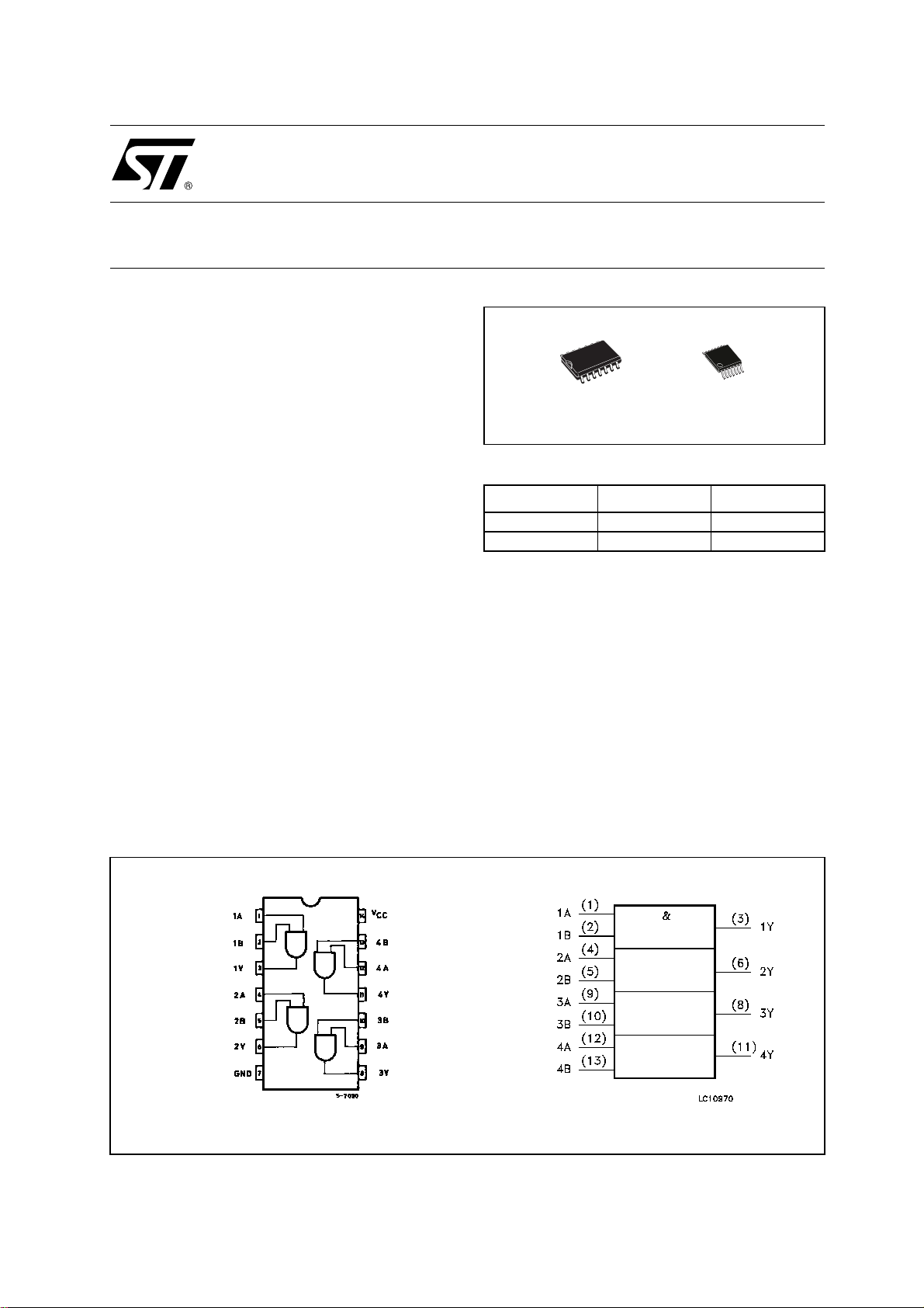
74VHC08
harman/kardon
AVR247/230 Service Manual
Page 59 of 131
QUAD 2-INPUT AND GATE
■ HIGH SPEED: t
■ LOW POWER DISSIPATION:
I
= 2 µA (MAX.) at TA=25°C
CC
■ HIGH NOISE IMMUNITY:
V
= V
NIH
■ POWER DOWN PROTECTION ON INPUTS
■ SYMMETRICAL OUTPUT IMPEDANCE:
|I
| = IOL = 8mA (MIN)
OH
■ BALANCED PROPAGATION DELAYS:
t
≅ t
PLH
■ OPERATI N G VOLTAGE RANGE:
V
(OPR) = 2V to 5.5V
CC
■ PIN AND FUNCTION COMPATIBLE WITH
= 28% VCC (MIN.)
NIL
PHL
= 4.3 ns (TYP.) at VCC = 5V
PD
74 SERIES 08
■ IMPROVED LATCH-UP IMMUNITY
■ LOW NOISE: V
= 0.8V (MAX.)
OLP
DESCRIPTION
The 74VHC08 is a n advanced high-speed CMOS
QUAD 2-INPUT AND GATE fabricated with
sub-micron silicon gate and double-layer metal
wiring C
2
MOS technology.
The internal circuit is composed of 2 stages
including buffer ou tput, which provides high no ise
immunity and stable output.
TSSOPSOP
ORDER CODES
PACKAGE TUBE T & R
SOP 74VHC08M 74VHC08MTR
TSSOP 74VHC08TTR
Power down protection is provided on all inputs
and 0 to 7V can be accepted on inputs with no
regard to the supply voltage. This device can be
used to interface 5V to 3V.
All inputs and outputs are equipped with
protection circuits against stat ic discharge, giving
them 2KV ESD immunity and transient excess
voltage.
PIN CONNECTION AND IEC LOGIC SYMBOLS
June 2001
Page 60

1
2
NC = NO CONNECT
V+
NC (OR V–)
V–
3
TOP
VIEW
QUANTITY
TEMPERATURE DRIFT – ppm/°C
0
–40
5
10
15
20
25
30
35
40
45
50
–30 –20 –10
0
10 20 30 40
QUANTITY
OUTPUT ERROR – mV
0
–10
50
100
150
200
250
300
–8 –6 –4 –2 0 2 4 10
68
1.2 V Micropower, Precision
harman/kardon
AVR247/230 Service Manual
Page 60 of 131
a
FEATURES
Wide Operating Range: 50 mA–10 mA
Initial Accuracy: 60.1% max
Temperature Drift: 650 ppm/8C max
Output Impedance: 0.5 V max
Wideband Noise (10 Hz–10 kHz): 20 mV rms
Operating Temperature Range: –408C to +858C
High ESD Rating
4 kV Human Body Model
400 V Machine Model
Compact, Surface-Mount, SOT-23 Package
GENERAL DESCRIPTION
The AD1580 is a low cost, two-terminal (shunt), precision
bandgap reference. It provides an accurate 1.225 V output for
input currents between 50 µA and 10 mA.
The AD1580’s superior accuracy and stability is made possible
by the precise matching and thermal tracking of on-chip
components. Proprietary curvature correction design techniques
have been used to minimize the nonlinearities in the voltage
output temperature characteristics. The AD1580 is stable with
any value of capacitive load.
The low minimum operating current makes the AD1580 ideal
for use in battery powered 3 V or 5 V systems. However, the
wide operating current range means that the AD1580 is
extremely versatile and suitable for use in a wide variety of high
current applications.
The AD1580 is available in two grades, A and B, both of which
are provided in an SOT-23 package, the smallest surface mount
package available on the market. Both grades are specified over
the industrial temperature range of –40°C to +85°C.
Shunt Voltage Reference
AD1580
PIN CONFIGURATION
SOT-23 Package
Reverse Voltage Temperature Drift Distribution
TARGET APPLICATIONS
1. Portable, Battery-Powered Equipment:
Cellular Phones, Notebook Computers, PDAs, GPS and
DMM.
2. Computer Workstations
Suitable for use with a wide range of video RAMDACs.
3. Smart Industrial Transmitters
4. PCMCIA Cards.
5. Automotive.
6. 3 V/5 V 8–12-Bit Data Converters.
REV. 0
Information furnished by Analog Devices is believed to be accurate and
reliable. However, no responsibility is assumed by Analog Devices for its
use, nor for any infringements of patents or other rights of third parties
which may result from its use. No license is granted by implication or
otherwise under any patent or patent rights of Analog Devices.
Reverse Voltage Error Distribution
© Analog Devices, Inc., 1995
One Technology Way, P.O. Box 9106, Norwood, MA 02062-9106, U.S.A.
Tel: 617/329-4700 Fax: 617/326-8703
Page 61

ADV7322 Preliminary Technical Data
harman/kardon
AVR247/230 Service Manual
Page 61 of 131
PIN CONFIGURATION AND FUNCTION DESCRIPTIONS
V
DD_IO
TEST0
TEST1
V
DGND
TEST2
TEST3
Y0
Y1
Y2
Y3
Y4
Y5
DD
Y6
Y7
C0
GND_IO63CLKIN_B62S761S660S559S458S357DGND56V
64
1
2
3
4
5
6
7
8
9
10
11
12
13
14
15
16
PIN 1
17C118C219
20
C
2
I
ALSB
DD
55S254S153S052
ADV7322
TOP VIEW
(Not to Scale)
21
22
23
24
25
26C327C428C529C630C731
SDA
SCLK
P_VSYNC
P_HSYNC
P_BLANK
Figure 19. Pin Configuration
TEST551TEST450S_HSYNC
S_VSYNC
49
48
47
46
45
44
43
42
41
40
39
38
37
36
35
34
33
32
CLKIN_A
RTC_SCR_TR
S_BLANK
R
SET1
V
REF
COMP1
DAC A
DAC B
DAC C
V
AA
AGND
DAC D
DAC E
DAC F
COMP2
R
SET2
EXT_LF
RESET
05067-019
Rev. PrA | Page 18 of 88
Page 62

Preliminary Technical Data ADV7322
harman/kardon
AVR247/230 Service Manual
Page 62 of 131
Table 6. Pin Function Descriptions
Mnemonic Input/Output Function
DGND G Digital Ground.
AGND G Analog Ground.
CLKIN_A I Pixel Clock Input for HD (74.25 MHz Only, PS Only (27 MHz), SD Only (27 MHz).
CLKIN_B I
COMP1,
O Compensation Pin for DACs. Connect 0.1 µF capacitor from COMP pin to V
COMP2
DAC A O CVBS/Green/Y/Y Analog Output.
DAC B O Chroma/Blue/U/Pb Analog Output.
DAC C O Luma/Red/V/Pr Analog Output.
DAC D O
DAC E O
DAC F O
P_HSYNC
P_VSYNC
P_BLANK
S_BLANK
S_HSYNC
S_VSYNC
I Video Horizontal Sync Control Signal for HD in Simultaneous SD/HD Mode and HD Only Mode.
I Video Vertical Sync Control Signal for HD in Simultaneous SD/HD Mode and HD Only Mode.
I Video Blanking Control Signal for HD in Simultaneous SD/HD Mode and HD Only Mode.
I/O Video Blanking Control Signal for SD Only.
I/O Video Horizontal Sync Control Signal for SD Only.
I/O Video Vertical Sync Control Signal for SD Only.
Y7 to Y0 I
C7 to C0 I
S7 to S0 I SD or Progressive Scan/HDTV Input Port for Cr [Red/V] data in 4:4:4 input mode. LSB is set up on Pin S0.
RESET
R
SET1
, R
SET2
I
I
SCLK I I2C Port Serial Interface Clock Input.
SDA I/O I2C Port Serial Data Input/Output.
ALSB I
V
P Power Supply for Digital Inputs and Outputs.
DD_IO
VDD P Digital Power Supply.
VAA P Analog Power Supply.
V
I/O Optional External Voltage Reference Input for DACs or Voltage Reference Output (1.235 V).
REF
EXT_LF I External Loop Filter for the Internal PLL.
RTC_SCR_TR I Multifunctional Input. Real time control (RTC) input, timing reset input, subcarrier reset input.
I2C I This input pin must be tied high (V
GND_IO Digital Input/Output Ground.
TEST0 to
I Not used. Tie to DGND
TEST5
Pixel Clock Input. Requires a 27 MHz reference clock for progressive scan mode or a 74.25 MHz (74.1758
MHz) reference clock in HDTV mode. This clock is only used in dual modes.
.
AA
In SD Only Mode: CVBS/Green/Y Analog Output; in HD Only Mode and Simultaneous HD/SD Mode:
Y/Green [HD] Analog Output.
In SD Only Mode: Luma/Blue/U Analog Output; in HD Only Mode and Simultaneous HD/SD Mode: Pr/Red
Analog Output.
In SD Only Mode: Chroma/Red/V Analog Output; in HD Only Mode and Simultaneous HD/SD Mode:
Pb/Blue [HD] Analog Output.
SD or Progressive Scan/HDTV Input Port for Y Data. Input port for interleaved progressive scan data. The
LSB is set up on Pin Y0.
Progressive Scan/HDTV Input Port 4:4:4 Input Mode. This port is used for the Cb [Blue/U] data. The LSB is
set up on Pin C0.
This input resets the on-chip timing generator and sets the ADV7322 into default register setting.
RESET
an active low signal.
A 3040 Ω resistor must be connected from this pin to AGND and is used to control the amplitudes of the
DAC outputs.
2
TTL Address Input. This signal sets up the LSB of the I
activated, which reduces noise on the I
2
C interface.
) for the ADV7322 to interface over the I2C port.
DD_IO
C address. When this pin is tied low, the I2C filter is
is
Rev. PrA | Page 19 of 88
Page 63

Features
harman/kardon
AVR247/230 Service Manual
Page 63 of 131
• Low-volta ge and Stand ard-voltage Operation
– 2.7 (VCC = 2.7V to 5.5V)
– 1.8 (V
• Internally Organized 128 x 8 (1K), 256 x 8 (2K), 512 x 8 (4K),
1024 x 8 (8K) or 2048 x 8 (16K)
• Two-wire Serial Interface
• Schmitt Trigger, Filtered Inputs for Noise Suppression
• Bidirectional Data Transfer Protocol
• 100 kHz (1.8V) and 400 kHz (2.7V, 5V) Compatibility
• Write Protect Pin for Hardware Data Protection
• 8-byte Page (1K, 2K), 16-byte Page (4K, 8K, 16K) Write Modes
• Partial Page Writes Allowed
• Self-timed Write Cycle (5 ms max)
• High-reliability
– Endurance: 1 Million Write Cycles
– Data Retention: 100 Years
• Automotive Grade and Lead-free/Halogen-free Devices Available
• 8-lead PDIP, 8-lead JEDEC SOIC, 8-lead MAP, 5-lead SOT23,
8-lead TSSOP and 8-ball dBGA2 Packages
• Die Sales: Wafer Form, Waffle Pack and B um pe d Wafers
= 1.8V to 5.5V)
CC
Two-wire
Serial EEPROM
1K (128 x 8)
2K (256 x 8)
4K (512 x 8)
8K (1024 x 8)
Description
The AT24C01A/02/04/08A/16A provides 1024/2048/4 096/8192/16384 bits of ser ial
electrically erasable and programmable read-only memor y (EEPROM) organized as
128/256/512/1024/2048 words of 8 bits each. The device is optimized for use in many
industrial and commercial applications where low-power and low-voltage operation
are essential. The A T24C01A/02/04/08A/16A is available in space-saving 8-lead PDIP,
8-lead JEDEC SOIC, 8-lead MAP, 5-lead SOT23 (AT24C01 A/AT24C02/AT24C04), 8lead TSSOP, and 8-ball dBGA2 packages and is accessed via a Two-wire serial interface. In addition, the entire family is available in 2.7V (2.7V to 5.5V) and 1.8V (1.8V to
5.5V) versions.
Table 1. Pin Configuration
Pin Name Function
A0 - A2 Address Inputs
SDA Serial Data
SCL Serial Clock Input
WP Write Protect
NC No Connect
GND Ground
VCC Power Supply
8-lead TSSOP
A0
A1
A2
GND
8-ball dBGA2
VCC
WP
SCL
SDA
Bottom View
8-lead PDIP
1
2
3
4
8
VCC
7
WP
6
SCL
5
SDA
1
8
7
6
5
A0
2
A1
3
A2
4
GND
GND
A0
A1
A2
8-lead MAP
VCC
8
WP
7
SCL
6
SDA
5
Bottom View
5-lead SOT23
8-lead SOIC
1
2
3
4
1
2
3
4
8
7
6
5
A0
A1
A2
GND
VCC
WP
SCL
SDA
16K (2048 x 8)
AT24C01A
AT24C02
AT24C04
AT24C08A
AT24C16A
A0
A1
A2
GND
1
2
3
4
8
VCC
7
WP
6
SCL
5
SDA
SCL
GND
SDA
1
2
3
WP
5
VCC
4
0180V–SEEPR–8/05
1
Page 64

3. Block Diagram
harman/kardon
AVR247/230 Service Manual
Page 64 of 131
Figure 2-1. 8-SOIC Top View
1
CS
SO
WP
GND
2
3
4
8
7
6
5
AT26DF081A [Preliminary]
VCC
HOLD
SCK
SI
CS
SCK
SI
INTERFACE
CONTROL
SO
WP
4. Memory Array
CONTROL AND
PROTECTION LOGIC
I/O BUFFERS
AND LATCHES
SRAM
DATA BUFFER
AND
LOGIC
Y-DECODER
Y-GATING
FLASH
MEMORY
X-DECODER
ARRAY
ADDRESS LATCH
To provide the greatest flexibility, the memory array of the AT26DF081A can be erased in four
levels of granularity including a full chip erase. In addition, the array has been divided into physical sectors of various si zes, of which each sector can be individually pr otected from progra m
and erase operations. The si zes of the physical sec tors are optim ized for bo th code and d ata
storage applicati ons, allowi ng both cod e and data segments to resid e in their ow n isolate d
regions. Th e Figure 4-1 on page 4 illustrates the breakdown of each erase level as well as the
breakdown of each physical sector.
3600A–DFLASH–11/05
Page 65

2. PIN DESCRIPTIONS
T
harman/kardon
AVR247/230 Service Manual
Page 65 of 131
CS42528
CX_SDIN1
CX_SCLK
CX_LRCK
VD
DGND
VLC
SCL/CCLK
SDA/CDOUT
AD1/CDIN
AD0/CS
INT
RST
AINR-
AINR+
AINL+
AINL-
CX_SDIN2
CX_SDIN4
CX_SDIN3
64 63 62 61 60 59 58 57 56 55 54 53 52 51 50 49
1
2
3
4
5
6
7
8
9
10
11
12
13
14
15
16
17 18 19 20 21 22 23 24 25 26 27 28 29 30 31 32
VQ
FILT+
REFGND
OMCK
SAI_SCLK
SAI_LRCK
CS42528
AOUTB4-
AOUTA4-
AOUTB4+
AOUTA4+
VA
AGND
AOUTB3-
AOUTB3+
AOUTA3+
VLS
SAI_SDOU
RMCK
CX_SDOUT
ADCIN2
ADCIN1
DGND
AOUTA3-
VD
AOUTB2-
TXP
AOUTB2+
RXP0
AOUTA2+
48
47
46
45
44
43
42
41
40
39
38
37
36
35
34
33
RXP1/GPO1
RXP2/GPO2
RXP3/GPO3
RXP4/GPO4
RXP5/GPO5
RXP6/GPO6
RXP7/GPO7
VARX
AGND
LPFLT
MUTEC
AOUTA1AOUTA1+
AOUTB1+
AOUTB1AOUTA2-
Pin Name # Pin Description
CX_SDIN1
CX_SDIN2
CX_SDIN3
CX_SDIN4
CX_SCLK 2 CODEC Serial Clock (Input/Output) - Serial clock for the CODEC serial audio interface.
CX_LRCK 3 CODEC Left Right Clock (Input/Output) - Determines which channel, Left or Right, is currently active on
VD 451Digital Power (Input) - Positive power supply for the digital section.
DGND 552Digital Ground (Input) - Ground reference. Should be connected to digital ground.
VLC 6
SCL/CCLK 7 Serial Control Port Clock (Input) - Serial clock for the serial control port. Requires an external pull-up
SDA/CDOUT 8 Serial Control Data (Input/Output) - SDA is a data I/O line in I
AD1/CDIN 9 Address Bit 1 (I2C)/Serial Control Data (SPI) (Input) - AD1 is a chip address pin in I
1
Codec Serial Audio Data Input (Input) - Input for two’s complement serial audio data.
64
63
62
the CODEC serial audio data line.
Control Port Power (Input) - Determines the required signal level for the control port.
resistor to the logic interface voltage in I
2
C mode as shown in the Typical Connection Diagram.
2
C mode and requires an external pull-up
resistor to the logic interface voltage, as shown in the Typical Connection Diagram. CDOUT is the output
data line for the control port interface in SPI mode.
2
C mode; CDIN is
the input data line for the control port interface in SPI mode.
Page 66

CS42528
harman/kardon
AVR247/230 Service Manual
Page 66 of 131
AD0/CS 10
Address Bit 0 (I2C)/Control Port Chip Select (SPI) (Input) - AD0 is a chip address pin in I
2
C mode; CS
is the chip select signal in SPI mode.
INT 11 Interrupt (Output) - The CS42528 will generate an interrupt condition as per the Interrupt Mask register.
See “Interrupts” on page 40 for more details.
RST 12 Reset (Input) - The device enters a low power mode and all internal registers are reset to their default
settings when low.
AINRAINR+
AINL+
AINL-
VQ 17 Quiescent Voltage (Output) - Filter connection for internal quiescent reference voltage.
FILT+ 18 Positive Voltage Reference (Output) - Positive reference voltage for the internal sampling circuits.
REFGND 19 Reference Ground (Input) - Ground reference for the internal sampling circuits.
AOUT A1 +,-
AOUTB1 +,AOUT A2 +,AOUTB2 +,AOUT A3 +,AOUTB3 +,AOUT A4 +,AOUTB4 +,-
VA
VARX
AGND 2540Analog Ground (Input) - Ground reference. Should be connected to analog ground.
13
Differential Right Channel Analog Input (Input) - Signals are presented differentially to the delta-sigma
14
modulators via the AINR+/- pins.
15
Differential Left Channel Analog Input (Input) - Signals are presented differentially to the delta-sigma
16
modulators via the AINL+/- pins.
36,37
Differential Analog Output (Output) - The full-scale differential analog output level is specified in the
35,34
Analog Characteristics specification table.
32,33
31,30
28,29
27,26
22,23
21,20
24
Analog Power (Input) - Positive power supply for the analog section.
41
MUTEC 38 Mute Control (Output) - The Mute Control pin outputs high impedance following an initial power-on con-
dition or whenever the PDN bit is set to a ‘1’, forcing the codec into power-down mode. The signal will
remain in a high impedance state as long as the part is in power-down mode. The Mute Control pin goes
to the selected “active” state during reset, muting, or if the master clock to left/right clock frequency ratio
is incorrect. This pin is intended to be used as a control for external mute circuits to prevent the clicks
and pops that can occur in any single supply system. The use of external mute circuits are not mandatory but may be desired for designs requiring the absolute minimum in extraneous clicks and pops.
LPFLT 39 PLL Loop Filte r (Output) - An RC network should be connected between this pin and ground.
RXP7/GPO7
RXP6/GPO6
RXP5/GPO5
RXP4/GPO4
RXP3/GPO3
RXP2/GPO2
RXP1/GPO1
RXP0 49 S/PDIF Receiver Input (Input) - Dedicated receiver input for S/PDIF encoded data.
TXP 50 S/PDIF T ransmitter Output (Output) - S/PDIF encoded data output, mapped directly from one of the
42
S/PDIF Receiver Input/ General Purpose Output (Input/Output) - Receiver inputs for S/PDIF encoded
43
data. The CS42528 has an internal 8:2 multiplexer to select the active receiver port, according to the
44
Receiver Mode Control 2 register. These pins can also be configur ed as general purpose output pins,
45
ADC Overflow indicators or Mute Control outputs according to the RXP/General Purpose Pin Control
46
registers.
47
48
receiver inputs as indicated by the Receiver Mode Control 2 register.
VLS 53 Serial Port Interface Power (Input) - Determines the required signal level for the serial port interfaces.
SAI_SDOUT
54 Serial Audio Interface Serial Data Output (Output) - Output for two’s complement serial audio PCM
data from the S/PDIF incoming stream. This pin can also be configured to transmit the output of the internal and external ADCs.
RMCK 55 Recovered Master Clock (Output) - Recovered master clock output from the External Clock Reference
(OMCK, pin 59) or the PLL which is locked to the incoming S/PDIF stream or CX_LRCK.
18 DS586PP5
Page 67

CS42528
harman/kardon
AVR247/230 Service Manual
Page 67 of 131
CX_SDOUT 56 CODEC Serial Data Output (Output) - Output for two’s complement serial audio data from the internal
and external ADCs.
ADCIN1
ADCIN2
OMCK 59 External Reference Clock (Input) - External clock reference that must be within the ranges specified in
SAI_LRCK 60 Serial Audio Interface Left/Right Clock (Input/Output) - Determines which channel, Left or Right, is
SAI_SCLK 61 Serial Audio Interface Serial Clock (Input/Output) - Serial clock for the Serial Audio Interface.
58
External ADC Serial Input (Input) - The CS42528 provides for up to two external stereo analog to digital
57
converter inputs to provide a maximum of six channels on one serial data output line when the CS42528
is placed in One Line mode.
the register “OMCK Frequency (OMCK Freqx)” on page 54.
currently active on the serial audio data line.
Page 68

3. TYPICAL CONNECTION DIAGRAM
harman/kardon
AVR247/230 Service Manual
Page 68 of 131
CS42528
+3.3 V to +5 V
+2.5 V
to +5 V
+1.8 V
to +5 V
** Resistors are required for
I
10 µF
10 µF
Driver
S/PDIF
Interfac e
Up to 8
Sources
CS5361
A/D Converter
A/D Converter
Digital A u dio
Processor
Micro-
Controller
2
C control port operation
0.1 µF 0.01 µF
+
0.1 µF
+
OSC
CS5361
2 kΩ 2 kΩ
0.01 µF
0.1 µF
** **
0.1 µF
VD
50
TXP
49
RXP0
48
RXP1/GPO1
47
RXP2/GPO2
46
RXP3/GPO3
45
RXP4/GPO4
44
RXP5/GPO5
43
RXP6/GPO6
42
RXP7/GPO7
53
59
OMCK
58
ADCIN1
57
ADCIN2
55
RMCK
54
60
61
3
CX_LRCK
2
CX_SCLK
56
CX_SDOUT
1
CX_SDIN1
64
CX_SDIN2
63
CX_SDIN3
62
CX_SDIN4
11
INT
12
RST
7
SCL/CCLK
8
SDA/CDOUT
9
AD1/CDIN
10
AD0/CS
6
VLC
DGND
4
VLS
51
CS42528
SAI_SDOUT
SAI_LRCK
SAI_SCLK
DGND
5
52 40
25
41
VAVD
24
VA
AOUTA1+
AOUTA1-
AOUTB1+
AOUTB1-
AOUTA2+
AOUTA2-
AOUTB2+
AOUTB2-
AOUTA3+
AOUTA3-
AOUTB3+
AOUTB3-
AOUTA4+
AOUTA4-
AOUTB4+
AOUTB4-
MUTEC
AINL+
AINL-
AINR+
AINR-
VQ
FILT+
REFGND
LPFLT
AGNDAGND
0.01 µF
0.01 µF
36
37
35
34
32
33
31
30
28
29
27
26
22
23
21
20
+VA
38
15
16
14
13
17
18
19
39
*
*
0.1 µF
RFILT
CFILT
0.1 µF
+
10 µF
0.1 µF
+
10 µF
Analog Output Buffer
and
Mute Circuit (optional)
Analog Output Buffer
and
Mute Circuit (optional)
Analog Output Buffer
and
Mute Circuit (optional)
Analog Output Buffer
and
Mute Circuit (optional)
Analog Output Buffer
and
Mute Circuit (optional)
Analog Output Buffer
and
Mute Circuit (optional)
Analog Output Buffer
and
Mute Circuit (optional)
Analog Output Buffer
and
Mute Circuit (optional)
Mute
Drive
(optional)
Analog
2700 pF*
Input
1
Buffer
Analog
Input
2700 pF*
1
Buffer
+
3
3
100 µF
CRIP
0.1 µF
3
+5 V
2
2
2
2
2
2
2
2
* Pull up or down as
required on startup if the
Mute Control is used.
Left Analog Input
Right Analog Inpu
+
4.7 µF
20 DS586PP5
1. See the ADC Input Filter section in the Appendix.
2. See the DAC Output Filter section in the Appendix.
3. See the PLL Filter section in the Appendix.
Figure 5. Typical Connection Diagram
Connect DGND and AGN D at single point near Codec
Page 69

harman/kardon
AVR247/230 Service Manual
Page 69 of 131
Page 70

harman/kardon
AVR247/230 Service Manual
Page 70 of 131
PRODUCT SELECTOR GUIDE
Family Part Number ES29LV800
Voltage Range 2.7 ~ 3.6V
Speed Option 70 90 120
Max Access Time (ns) 70 90 120
CE# Access (ns) 70 90 120
OE# Access (ns) 30 35 50
FUNCTION BLOCK DIAGRAM
RY/BY#
ESI
ESI
Excel Semiconductor inc.
Vcc
Vss
WE
RESET#
A<0:18>
CE#
OE#
BYTE#
Vcc Detector
#
Command
Register
Chip Enable
Output Enable
Logic
Timer/
Counter
Write
State
Machine
Analog Bias
Generator
Sector Switches
Y-Decoder
X-Decoder
Address Latch
DQ0-DQ15(A-1)
Input/Output
Buffers
Data Latch/
Sense Amps
Y-Decoder
Cell Array
ES29LV800E
3
Rev. 0A January 5, 2006
Page 71

harman/kardon
AVR247/230 Service Manual
Page 71 of 131
PIN DESCRIPTION
Pin Description
A0-A18 19 Addresses
DQ0-DQ14 15 Data Inputs/Outputs
DQ15/A-1
CE# Chip Enable
OE# Output Enable
WE# Write Enable
RESET# Hardware Reset Pin, Active Low
BYTE# Selects 8-bit or 16-bit mode
RY/BY# Ready/Busy Output
Vcc
Vss Device Ground
NC Pin Not Connected Internally
Excel Semiconductor inc.
DQ15 (Data Input/Output, Word Mode)
A-1 (LSB Address Input, Byte Mode)
3.0 volt-only single power supply
(see Product Selector Guide for speed options and voltage supply tolerances)
ESI
ESI
LOGIC SYMBOL
19
A0 ~ A18
CE#
OE#
WE#
RESET#
BYTE#
16 or 8
DQ0 ~ DQ15
(A-1)
RY/BY#
ES29LV800E
4
Rev. 0A January 5, 2006
Page 72

harman/kardon
AVR247/230 Service Manual
Page 72 of 131
CONNECTION DIAGRAM
ESI
ESI
Excel Semiconductor inc.
A15
A14
A13
A12
A11
A10
A9
A8
NC
NC
WE#
RESET#
NC
NC
RY/BY#
A18
A17
A7
A6
A5
A4
A3
A2
A1
1
2
3
4
5
6
7
8
9
10
11
12
13
14
15
16
17
18
19
20
21
22
23
24
48-Pin Standard TSOP
ES29LV800
48
47
46
45
44
43
42
41
40
39
38
37
36
35
34
33
32
31
30
29
28
27
26
25
A16
BYTE#
Vss
DQ15/A-1
DQ7
DQ14
DQ6
DQ13
DQ5
DQ12
DQ4
Vcc
DQ11
DQ3
DQ10
DQ2
DQ9
DQ1
DQ8
DQ0
OE#
Vss
CE#
A0
48-Ball FBGA (6 x 8 mm)
(Top View, Balls Facing Down)
A B C D E F G H
6
5
4
3
2
1
A13 A12
A9
WE#
RY/
BY#
A7
A3
A8
RESET#
NC
A17
A4
A14
A10
NC
A18
A6
A2
A15
A16
A11 DQ7
NC
NC
A5
DQ5
DQ2
DQ0
A0A1
BYTE#
DQ14
DQ12
DQ10 DQ11 DQ3
DQ8 DQ9 DQ1
DQ15/
A-1
DQ13
Vcc
OE#CE#
Vss
DQ6
DQ4
Vss
ES29LV800E
5
Rev. 0A January 5, 2006
Page 73

ANALOG MULTIPLEXER/DEMULTIPLEXER
harman/kardon
AVR247/230 Service Manual
Page 73 of 131
■ LOW "ON" RESISTANCE : 125Ω (Typ.)
OVER 15V p.p SIGNAL-INPUT RANGE FOR
V
DD-VEE
■ HIGH "OFF" RESISTANCE : CHANNEL
LEAKAGE ± 100pA (Typ.) at V
■ BINARY ADDRESS DECODING ON CHIP
■ HIGH DEGREE OF LINEARITY : < 0.5%
DISTORTIONTYP. at f
V
DD-VSS
■ VERY LOW QUIESCENT POWER
DISSIPATION UNDER ALL DIGITAL
CONTROL INPUT AND SUP PLY
CONDITIONS : 0.2
at V
■ MATCHED SWITCH CHARACTERISTICS :
R
ON
■ WIDE RANGE O F DIGITAL AND ANALOG
SIGNAL LEVELS : DIGITAL 3 to 20,
ANALOG TO 20V p.p.
■ QUIESCENT CURRENT SPECIF. UP TO 20V
■ 5V, 10V AND 15V PARAM ETRIC RATINGS
■ INPUT LEAKAGE CURRENT
I
= 100nA (MAX) AT VDD=18VTA= 25°C
I
■ 100% TESTED FOR QUIESCENT CURRENT
■ MEETS ALL REQUIREMENTS OF JEDEC
JESD13B " STANDARD SPECIFICATIONS
FOR DESCRIPTIONOF B SERIES CMOS
DEVICES"
DESCRIPTION
The HCF4053B is a monolithic integrated circuit
fabricated in Metal Oxide Semiconductor
= 15V
DD-VEE
=1KHz,VIS=5Vpp,
IS
> 10V, RL = 10KΩ
µW(Typ.)
DD-VSS=VDD-VEE
=10V
=5Ω (Typ.) FOR VDD-VEE= 15V
=18V
HCF4053B
TRIPLE 2-CHANNEL
DIP SOP
ORDER CODES
PACKAGE TUBE T & R
DIP HCF4053BEY
SOP HCF4053BM1 HCF4053M013TR
technology available in DIP and SOP packages.
The HCF4053B analog m ultipl ex er/de mul tiplexer
is a digitally controlled analog switch having low
ON impedance and very low OFF leakage current.
This multiplexer circuit dissipate extremely low
quiescent power over the full V
V
supply voltage rang e, independent of the
EE
DD-VSS
logic state of the control signals.
When a logic "1" is present at the inhibit input
terminal all ch annel are off. This de vice is a triple
2-channel multiplexe r having t hree separate
digital control inputs, A, B, and C, and an inhibit
input. Eac h control input selects one of a pair of
channels w hich are connected in a single pole
double-throw configuration.
and VDD-
PIN CONNECTION
October 2002
Page 74

harman/kardon
AVR247/230 Service Manual
Page 74 of 131
Page 75

Pin Assignment (DIP16/MFP16)
No. 6037-2/8
LC72723, LC72723M
Block Diagram
harman/kardon
AVR247/230 Service Manual
Page 75 of 131
Page 76

PIN CONFIGURATION
harman/kardon
AVR247/230 Service Manual
Page 76 of 131
HY57V161610E
V
V
DD
DD
DQ0
DQ0
DQ1
DQ1
V
V
SSQ
SSQ
DQ2
DQ2
DQ3
DQ3
V
V
DDQ
DDQ
DQ4
DQ4
DQ5
DQ5
V
V
SSQ
SSQ
DQ6
DQ6
DQ7
DQ7
VDDQ
VDDQ
LDQM
LDQM
/WE
/WE
/CAS
/CAS
/RAS
/RAS
/CS
/CS
A11
A11
A10
A10
A0
A0
A1
A1
A2
A2
A3
A3
V
V
DD
DD
1
1
2
2
3
3
4
4
5
5
6
6
7
7
8
8
9
9
10
10
11
11
12
12
13
13
14
14
15
15
16
16
17
17
18
18
19
19
20
20
21
21
22
22
23
23
24
24
25
25
50pin TSOP II
50pin TSOP II
400mil x 825mil
400mil x 825mil
0.8mm pin pitch
0.8mm pin pitch
50
50
49
49
48
48
47
47
46
46
45
45
44
44
43
43
42
42
41
41
40
40
39
39
38
38
37
37
36
36
35
35
34
34
33
33
32
32
31
31
30
30
29
29
28
28
27
27
26
26
V
V
SS
SS
DQ15
DQ15
DQ14
DQ14
VSSQ
VSSQ
DQ13
DQ13
DQ12
DQ12
VDDQ
VDDQ
DQ11
DQ11
DQ10
DQ10
VSSQ
VSSQ
DQ9
DQ9
DQ8
DQ8
VDDQ
VDDQ
NC
NC
UDQM
UDQM
CLK
CLK
CKE
CKE
NC
NC
A9
A9
A8
A8
A7
A7
A6
A6
A5
A5
A4
A4
VSS
VSS
PIN DESCRIPTION
PIN PIN NAME DESCRIPTION
CLK Clock
CKE Clock Enable
CS
BA Bank Address Select either one of banks during both RAS
A0 ~ A10 Address
, CAS, WE
RAS
LDQM, UDQM Data Input/Output Mask DQM control output buffer in read mode and mask input data in write mode
DQ0 ~ DQ15 Data Input/Output Multiplexed data input / output pin
DD/VSS Power Supply/Ground Power supply for internal circuit and input buffer
V
DDQ/VSSQ Data Output Power/Ground Power supply for DQ
V
NC No Connection No connection
Chip Select Command input enable or mask except CLK, CKE and DQM
Row Address Strobe,
Column Address Strobe, Write
Enable
The system clock input. All other inputs are referenced to the SDRAM on the rising
edge of CLK.
Controls internal clock signal and when deactivated, the SDRAM will be one of the
states among power down, suspend or self refresh.
and CAS activity.
Row Address : RA0 ~ RA10, Column Address : CA0 ~ CA7
Auto-precharge flag : A10
, CAS and WE define the operation.
RAS
Refer function truth table for details
Rev. 0.2 / Aug. 2003 2
Page 77

IDTQS3VH16233
harman/kardon
AVR247/230 Service Manual
Page 77 of 131
2.5V / 3.3V 32:16 MUX/DEMUX HIGH BANDWIDTH BUS SWITCH
INDUSTRIAL TEMPERATURE RANGE
PIN CONFIGURATION
4B1
4
6B1
6
8B1
8
GND
Vcc
10B1
10
11
12B1
12
13
14B1
14
15
16B1
16
TEST
TEST
3A
B2
5
B2
7
B2
9
B2
B2
B2
B2
4
5
6
7
A
8
9
10
A
11
12
13
14
15
A
16
17
18
A
19
20
21
A
22
23
24
A
26
1
27
28
2
5611A 1B1
5522B11B2
5432B22A
53
52
51
50
49
48
47
46
45
44
43
42
41
40
39
38
37
36
35
34
33
3225
31
30
29
3
3
4
5B1
5
6
7B1
7
8
GND
Vcc
9B1
9
10
11B1
11
12
13B1
13
14
15B1
15
16
SEL1
SEL2
B1
B2
A
B2
A
B2
A
B2
A
B2
A
B2
A
B2
A
ABSOLUTE MAXIMUM RATINGS
(1)
Symbol Description Max. Unit
(2)
VTERM
VTERM
VTERM
Supply Voltage to Ground – 0.5 to 4.6 V
(3)
DC Switch Voltage VS – 0.5 to 5.5 V
(3)
DC Input Voltage VIN – 0.5 to 5.5 V
VAC AC Input Voltage (pulse width ≤20ns) – 3 V
IOUT DC Output Current (max. current/pin) 12 0 mA
TSTG Storage Temperature -65 to +150 °C
NOTES:
1. Stresses greater than those listed under ABSOLUTE MAXIMUM RATINGS may
cause permanent damage to the device. This is a stress rating only and functional
operation of the device at these or any other conditions above those indicated in the
operational sections of this specification is not implied. Exposure to absolute
maximum rating conditions for extended periods may affect reliability.
2. VCC terminals.
3. All terminals except VCC.
CAPACITANCE (TA = +25
Symbol Parameter
(1)
o
C, f = 1MHz, VIN = 0V, VOUT = 0V)
Typ. Max. Unit
CIN Control Inputs 3 5 pF
CI/O Quickswitch Channels Mux 8 12 pF
(Switch OFF) Demux 4 6
CI/O Quickswitch Channels Mux 16 2 4 p F
(Switch ON) Demux 8 12
NOTE:
1. This parameter is guaranteed but not production tested.
PIN DESCRIPTION
Pin Names I/O Description
x A I/O Bus A
x Bx I /O Bus B
SELx I Data Select
TESTx I Port Select
SSOP/ TSSOP
TOP VIEW
FUNCTION TABLE
(1)
SELx TESTx xA Function
LLxB1 xA to xB1
HLxB2 xA to xB2
XHxB1, xB2 xA to xB1 and xB2
NOTE:
1. H = HIGH Voltage Level
L = LOW Voltage Level
X = Don't Care
2
Page 78

harman/kardon
AVR247/230 Service Manual
Page 78 of 131
Page 79

harman/kardon
AVR247/230 Service Manual
Page 79 of 131
Page 80

harman/kardon
AVR247/230 Service Manual
Page 80 of 131
Page 81

harman/kardon
AVR247/230 Service Manual
Page 81 of 131
Page 82

Figure 3: Connection Diagr am (top view)
harman/kardon
AVR247/230 Service Manual
Page 82 of 131
L7800 SERIES
TO-220 (Any Type)
2
PAK (Any Ty p e )
TO-220FP/TO-220FM
TO-3D
Table 3: Order Codes
2
PAK
TYPE
L7805 L7805T
L7805C L7805CV L7805C-V L7805CV1 L7805CD2T L7805C-D2TR L7805CP L7805CF L7805CT
L7852C L7852CV L7852CD2T L7852CP L7852CF L7852CT
L7806 L7806T
L7806C L7806CV L7806C-V L7806CD2T L7806CP L7806CF L7806CT
L7808 L7808T
L7808C L7808CV L7808C-V L7808CD2T L7808CP L7808CF L7808CT
L7885C L7885CV L7885CD2T L7885CP L7885CF L7885CT
L7809C L7809CV L7809C-V L7809CD2T L7809CP L7809CF L7809CT
L7810C L7810CV L7810CD2T L7810CP
L7812 L7812T
L7812C L7812CV L7812C-V L7812CD2T L7812CP L7812CF L7812CT
L7815 L7815T
L7815C L7815CV L7815C-V L7815CD2T L7815CP L7815CF L7815CT
L7818 L7818T
L7818C L7818CV L7818CD2T L7818CP L7818CF L7818CT
L7820 L7820T
L7820C L7820CV L7820CD2T L7820CP L7820CF L7820CT
L7824 L7824T
L7824C L7824CV L7824CD2T L7824CP L7824CF L7824CT
(*) Avai l abl e in Tape & Reel wi th the suffix " -T R".
TO-220
(A Typ e)
TO-220
(C Type)
TO-220
(E Type)
2
D
PAK
(A Type) (*)
D
(C Type)
(T & R)
TO-220FP TO-220FM TO-3
3/34
Page 83

L7900
harman/kardon
AVR247/230 Service Manual
Page 83 of 131
ABSOLUTE MAXIMUM RATINGS
Symbol Parameter Value Unit
DC Input Voltage (for VO= 5 to18V)
V
i
OutputCurrent Internally limited
I
o
PowerDissipation Internally limited
P
tot
T
Operating JunctionTemperatureRange 0 to 150
op
Storage Temperature Range - 65 to 150
T
stg
(forV
= 20,24V)
O
THERMALDATA
Symbol Parameter D2PAK TO-220 ISOWATT220 TO-3 Unit
R
thj-cas e
R
thj-amb
Thermal Resistance Junction-case Max
Thermal Resistance Junction-ambient Max
3
62.5
50
3
60
CONNECTION DIAGRAM AND ORDERING NUMBERS (top view)
-35
-40
4
4
35
o
o
V
V
o
C
o
C
C/W
C/W
TO-220 & ISOWATT220 TO-3D2PAK
Type TO-220 D
L7905C
L7952C
L7906C
L7908C
L7912C
L7915C
L7918C
L7920C
L7922C
L7924C
(*) AVAILABLE IN TAPE AND REEL WITH ”-TR” SUFFIX
L7905CV
L7952CV
L7906CV
L7908CV
L7912CV
L7915CV
L7918CV
L7920CV
L7922CV
L7924CV
2
L7905CD2T
L7952CD2T
L7906CD2T
L7908CD2T
L7912CD2T
L7915CD2T
L7918CD2T
L7920CD2T
L7922CD2T
L7924CD2T
APPLICATION CIRCUIT
PAK (*) ISOWATT220 TO-3 Output Voltage
L7905CP
L7906CP
L7908CP
L7912CP
L7915CP
L7918CP
L7920CP
L7924CP
L7905CT
L7952CT
L7906CT
L7908CT
L7912CT
L7915CT
L7918CT
L7920CT
L7922CT
L7924CT
-5V
-5.2V
-6V
-8V
-12V
-15V
-18V
-20V
-22V
-24V
2/13
Page 84

1A LOWDROP OUT VOLTAGE REGULATOR (ADJUSTABLE & FIXED) LM1117
harman/kardon
AVR247/230 Service Manual
Page 84 of 131
FEATURES
SOT-223 PKG (FRONT VIEW)
● Output Current up to 1 A
● Low Dropout Voltage ( 700mV at 1A Output Current )
● Three Terminal Adjustable or Fixed 1.5V, 1.8V, 2.5V, 2.85V,
3.0V, 3.3V, 5.0V
● 2.85V Device for SCSI-II Active Terminator
● 0.04% Line Regulaion, 0.1% Load Regulation
1 2 3
PIN FUNCTION
1. Adj/Gnd
2. Vout
3. Vin
● Very Low Quiescent Current
● Internal Current andTerminal Limit
● Logic-Controlled Electronics Shutdown
TO-263 (D2 PKG, FRONT VIEW)
● Surface Mount Package SOT-223 & TO-263 (D2-Pack)
● 100% Thermal Limit Burn-In
PIN FUNCTION
APPLICATION
1. Adj/Gnd
2. Vout
3. Vin
● Active SCSI Terminators
● Portable/Plan Top/Notebook Computers
● High Efficiency Linear Regulators
● SMPS Post Regulators
● Mother B/D Clock Supplies
● Disk Drives
● Battery Chargers
DESCRIPTION
1 2 3
ORDERING INFORMATION
Device (Marking)
LM1117S
LM1117S-XX
LM1117T
LM1117T-XX
(X=Output Voltage=1.5V, 1.8V, 2.5V, 2.85V,
'3.0V, 3.3V, 5.0V, Adjustable=AD)
Package
SOT-223
TO-263 (D2)
The LM1117 is a low power positive-voltage regulator designed to meet 1A output current and comply
with SCSI-II specifications with a fixed output voltage of 2.85V. This device is an excellent choice for use
in battery-powered applications, as active terminators for the SCSI bus, and portable computers.
The LM1117 features very low quiescent current and very
low dropout voltage of 700mV at a full load and
lower as output current decreases. LM1117 is available as an adjustable or fixed 1.5V, 1.8V, 2.5V, 2.85V,
3.0V, 3.3V, and 5.0V output voltages.
The LM1117 is offered in a 3-pin surface mount package SOT-223 & TO-263. The output capacitor of
10㎌ or larger is needed for output stability of LM1117 as required by most of the other regulator circuits.
ABSOLUTE MAXIMUM RATINGS
DC Input Voltage
Lead Temperature (Soldering, 5 Seconds)
Storage Temperature Range
Operating Junction Temperature Range
CHARACTERISTIC
SYMBOL
V
IN
T
SOL
T
STG
T
OPR
MIN. UNIT
-65 150
0
MAX.
7
260
125
V
℃
℃
℃
HTC
1
Page 85

M24C64, M24C32
harman/kardon
AVR247/230 Service Manual
Page 85 of 131
SUMMARY DESCRIPTION
These I2C-compatible electrically erasable programmable memory (EEPROM) devices are organized as 8192 x 8 bits (M24C64) and 4096 x 8 bits
(M24C32).
Table 2. Signal Names
E0, E1, E2 Chip Enable
SDA Serial Data
Figure 2. Logic Diagram
V
CC
3
E0-E2 SDA
SCL
WC
2
I
C uses a two-wire serial interf ace, comprisi ng a
M24C64
M24C32
V
SS
AI01844B
bi-directional data line and a clock line. The devices carry a built-in 4-bit Device Type Identifier code
(1010) in accordance with the I
The device behaves as a slave in the I
2
C bus definition.
2
C protocol,
with all memory operations synchronized by the
serial clock. Read and Write operations are initiated by a Start condition, generated by the bus master. The Start condition is followed by a Device
Select Code and Read/Write
bit (RW) (as described in Table 3.), terminated by an acknowledge bit.
When writing data to the memory, the dev ice inserts an acknowled ge bit during the 9
th
bit time,
following the bus master’s 8-bit transmission.
When data is read by the bus master, the bus
master acknowledge s the rec eipt o f the d ata by te
in the same way. Data transfers are terminated by
a Stop condition after an Ack for Write, and after a
NoAck for Read.
SCL Serial Clock
WC
V
CC
V
SS
Power On Reset: V
Write Control
Supply Voltage
Ground
Lock-Out Write Protect
CC
In order to prevent data corruption and inadvertent
Write operations during Power-up, a Power On
Reset (POR) circuit is included . At Power-up, the
internal reset i s he ld a cti ve unti l V
has reached
CC
the Power On Reset (POR) threshold voltage, and
all operations are disabled – the device will not respond to any command. In the sam e way, when
V
drops from the operat ing voltage, below the
CC
Power On Reset (PO R) threshold voltage, a ll operations are disa bled and the device will not respond to any command.
A stable and valid V
(as defined in Table 9. and
CC
Table 10.) must be applied before applying any
logic signal.
Figure 3. DIP, SO, TSSOP and UFDFPN
Connections
M24C64
M24C32
1
E0 V
2
3
E2
4
SS
Note: See PACKAGE MECHANICAL section for package dimen-
sions, and how to identify pin-1.
8
7
6
5
AI01845C
CC
WCE1
SCL
SDAV
4/26
Page 86

www.fairchildsemi.com
harman/kardon
AVR247/230 Service Manual
Page 86 of 131
MC78XX/LM78XX/MC78XXA
3-Terminal 1A Positive Voltage Regulator
Features
• Output Current up to 1A
• Output Voltages of 5, 6, 8, 9, 10, 12, 15, 18, 24V
• Thermal Overload Protection
• Short Circuit Protection
• Output Transistor Safe Operating Area Protection
Description
The MC78XX/LM78XX/MC78XXA series of three
terminal positive regulators are available in the
TO-220/D-PAK package and with several fixed output
voltages, making them useful in a wide range of
applications. Each type employs internal current limiting,
thermal shut down and safe operating area protection,
making it essentially indestructible. If adequate heat sinking
is provided, they can deliver over 1A output current.
Although designed primarily as fixed voltage regulators,
these devices can be used with external components to
obtain adjustable voltages and currents.
TO-220
1
D-PAK
1
1. Input 2. GND 3. Output
Internal Block Digram
©2001 Fairchild Semiconductor Corporation
Rev. 1.0.1
Page 87

harman/kardon
AVR247/230 Service Manual
Page 87 of 131
Page 88

harman/kardon
AVR247/230 Service Manual
Page 88 of 131
Page 89

harman/kardon
AVR247/230 Service Manual
Page 89 of 131
Page 90

312
harman/kardon
AVR247/230 Service Manual
Page 90 of 131
LOW DROPOUT VOLTAGE REGULATOR
GENERAL DESCRIPTION PACKAGE OUTLINE
The NJM2391 is low dropout voltage regulators
featuring high precision voltage.
It is suitable for Notebook PCs, PC cards and hard
disks where 3.3V need to be generat ed from 5V supply.
A small TO-252 package is adopted for the space
saving.
FEA TURES
zOutput Current Io(max.)=1A
zHigh Precision Output Voltage Vo±1%
zLow Dropout Voltage ∆ V
=1.1V typ. At Io=1A
I-O
zInternal Excessive Voltage Protect ion Circuit
zInternal Short Circuit Current Limit
zInternal Thermal Overload Protection
zBipolar Technology
zPackage Outline TO-252
PIN CONFIGURATION
PIN FUNCTION
1.V
IN
2.GND
OUT
3.V
NJM2391DL1
NJM2391
NJM2391DL1
ABSOLUTE MAXIMUM RATINGS (Ta=25°C)
PARAMETER SYMBOL RATINGS UNIT
Input Voltage V+ +10 V
Power Dissipation PD TO-252
Operating Temperature
Storage Temperature
Topr
Tstg
8 (Tc=25°C)
0.8(Ta≤25°C)
W
−40 ~ +85 °C
−50 ~ +125 °C
OUTPUT VOLTAGE RANK LIST
Device Name V
OUT
NJM2391DL1-25 2.5V
NJM2391DL1-26 2.6V
NJM2391DL1-28 2.85V
NJM2391DL1-03 3.0V
NJM2391DL1-33 3.3V
NJM2391DL1-35 3.5V
NJM2391DL1-05 5.0V
Page 91

harman/kardon
AVR247/230 Service Manual
Page 91 of 131
NJM2595
5-INPUT 3-OUTPUT VIDEO SWITCH
■ GENERAL DESCRIPTION ■ PACKAGE OUTLINE
The NJM2595 is a 5-input 3-output video switch. It s sw it ches
select one from five signals received from VTR,TV,DVD,
TV-GA M E and others.
The NJM2595 is designed for audio items, such as A V amplifier
and others.
NJM2595D NJM2595M
■ FEATURES
● 5-input 3-output
● Operating Voltage ±4.0 to ±6.5V
● Operating current ±15mAtyp. at Vcc=±5V
● Crosstalk -65dBtyp.
● Internal 6dB Amplifier
● Internal 75Ω Driver
● Bipolar Technology
● Package Outline DIP16,DMP16
■ PIN CONFIGURATION and BLOCK DIAGRAM
16
+
SW2V
10 14 2
SW1
SW5
Vin1
Vin2
Vin3
Vin4
Vin5
13
20k
20k
20k
S5
S6
S7
6dB
Amp
6dB
Amp
6dB
Amp
8 12 6 4
-
75Ω
Driver
75Ω
Driver
75Ω
Driver
1
15
11
Vout1
Vout2
Vout3
9
20k
7
20k
5
20k
3
20k
S2
S3
SW3
S4
SW4
S1
GND V
-1 -
Page 92

3
2
8
3 4
5
3
harman/kardon
AVR247/230 Service Manual
Page 92 of 131
NJM2845/46
LOW DROPOUT VOLTAGE REGULA TOR
GENERAL DESCRI PTION PACKAGE O UTLINE
The NJM2845 is low dropout voltage regulator. Advanced
Bipolar technology achieves low noise, high ripple rejection
and low quiescent current.
NJM2845 is 3 terminal type and NJM2846 is ON/OFF control
built in type. These product can be selected according to the
applications.
FEATURES
High Ripple Rejection 75dB typ. (f=1kHz,3V V ersion)
Output Noise V oltage Vno=45µVrms typ. (V o=3V V ersion)
Output capacitor with 2.2µF ceramic capacitor (Vo≥2.6V)
Output Current Io(max.)=800mA
High Precision Output Vo ±1.0%
Low Dropout V oltage 0.18V typ. (Io=500mA)
ON/OFF Control (NJM2846)
Internal Short Circuit Current Limit
Internal Thermal Overload Protection
Bipolar Technology
Package Outline TO-252-3 (NJM2845DL1), TO-252-5 (NJM2846DL3)
PIN CONFIG URA TION
1.V
IN
2.GND
3.V
OUT
1.CONTROL
2.V
IN
3.GND
4.V o
1
1 2
5.NC
NJM2845DL1
NJM2846DL3
NJM2845DL1 NJM2846DL3
EQUIVALENT CIRCUI T
V IN
GND
V
OUT
Thermal
Protection
Bandga p
Reference
V
Control
GND
IN
NJM2845DL1
Ver.2005-01-20
Bandgap
Reference
NJM2
Therma l
Protection
46DL3
V
OUT
-1-
Page 93

harman/kardon
AVR247/230 Service Manual
Page 93 of 131
Page 94

harman/kardon
AVR247/230 Service Manual
Page 94 of 131
Page 95

harman/kardon
AVR247/230 Service Manual
Page 95 of 131
Page 96

harman/kardon
AVR247/230 Service Manual
Page 96 of 131
Page 97

•
TO-92
PIN CONFIGURATION
•
SOT-89
•
SOT-23-5
PIN DESCRIPTION
•
TO-92
•
SOT-89
•
SOT-23-5
Pin No Symbol
1 OUT
2 VDD
3 GND
4 NC
5 NC
Pin No Symbol
1 OUT
2 VDD
3 GND
Pin No Symbol
1 OUT
2 VDD
3 GND
R×5VL
5
harman/kardon
AVR247/230 Service Manual
Page 97 of 131
(mark side)
1 2
3
(mark side)
1 2
5
4
(mark side)
3
1 2
3
Page 98
RN5RZ
3
PIN CONFIGURATION
PIN DESCRIPTION
• SOT-23-5
1 2
3
5 4
(mark side)
Pin No. Symbol Description
1 GND Ground Pin
2 VDD
Input Pin
3 VOUT Output Pin
4 NC No Connection
5 CE or CE Chip Enable Pin
ABSOLUTE MAXIMUM RATINGS
ABSOLUTE MAXIMUM RATINGS
Absolute Maximum ratings are threshold limit values that must not be exceeded even for an instant under
any conditions. Moreover, such values for any two items must not be reached simultaneously. Operation
above these absolute maximum ratings may cause degradation or permanent damage to the device. These
are stress ratings only and do not necessarily imply functional operation below these limits.
Symbol Item Ratings Unit
VIN Input Voltage 9 V
VCE Input Voltage (CE or CE Pin) –0.3 to VIN +0.3 V
VOUT Output Voltage –0.3 to VIN +0.3 V
IOUT Output Current 200 mA
PD Power Dissipation 250 mW
Topt Operating Temperature –40 to +85 ˚C
Tstg Storage Temperature –55 to +125 ˚C
harman/kardon
AVR247/230 Service Manual
Page 98 of 131
Page 99

harman/kardon
AVR247/230 Service Manual
Page 99 of 131
Page 100

SiI 9031 HDMI PanelLink Cinema Receiver
harman/kardon
AVR247/230 Service Manual
Page 100 of 131
Data Sheet
Pin Diagram
DGND
DVCC18
IOGND
IOVCC
MUTEOUT
SPDIF
CVCC
CGND
SD3
SD2
SD1
SD0
WS
SCK
MCLKIN
MCLKOUT
IOVCC
IOGND
CGND
CVCC18
NC
AUDPVCC18
AUDPGND
XTALOUT
XTALIN
XTALVCC
REGVCC
NC
RSVDL
RESET#
SCDT
INT
CVCC18
CGND
CLK48B
IOGND
73
74
75
76
77
78
79
80
81
82
83
84
85
86
87
88
89
90
91
92
93
94
95
96
97
98
99
100
101
102
103
104
105
106
107
108
AGND
R1X2+
72
AGND
R1X2-
71
70
R1X1-
AVCC
R1X1+
AVCC
65
67
68
66
69
AGND
64
AVCC
R1X0-
AGND
R1X0+
60
63
61
62
AVCC
R1XC+
R1XC-
58
59
57
AGND
PVCC1
RSVD_A
56
55
TMDSPGND
R0X2+
R0X2-
AGND
AVCC
54
50
52
53
51
49
AGND
R0X1-
R0X1+
AVCC
R0X0+
46
48
44
47
45
SiI 9031
144-Pin
TQFP
(Top View)
R0XC+
R0X0-
43
AVCC
42
R0XC-
PVCC0
AGND
41
AVCC
38
37
40
39
36
DGND
35
DVCC18
34
R0PWR5V
33
R1PWR5V
32
DSCL0
31
DSDA0
DSCL1
30
DSDA1
29
CSCL
28
27
CSDA
26
IOVCC
25
IOGND
CGND
24
CVCC18
23
22
DACDVCC18
21
DACDGND
AnBPb
20
DACVCCB
19
18
DACGNDB
AnGY
17
DACVCCG
16
DACGNDG
15
14
AnRPr
DACVCCR
13
DACGNDR
12
COMP
11
RSET
10
VREF
9
8
DACAGND
DACAVCC
7
6
DACOVCC
5
IOVCC
IOGND
4
3
VSYNC
2
HSYNC
DE
1
Individual pin functions are described beginning on page 37.
SiI-DS-0118-A 8
109
IOVCC
113
111
110
112
Q23
Q21
Q22
Q20
117
115
114
CGND
CVCC18
119
116
118
Q17
Q19
Q18
122
120
121
Q16
ODCK
IOVCC
IOGND
126
124
123
125
Q15
Q13
Q14
Q12
127
CGND
130
128
129
Q11
Q10
CVCC18
134
132
131
133
Q8
Q7
Q9
IOVCC
138
136
135
137
139
Q5
Q6
CGND
IOGND
142
140
Q4
CVCC18
144
141
143
Q3
Q2
Q1
Q0
Figure 1. Pin Diagram
 Loading...