Page 1
11
2
3
4
7
8
11
14
15
34
Page 2
SAFETY PRECAUTIONS
WARNING
Before servicing this unit, familiarize yourself with the following precautions:
1. Many electrical and mechanical parts in this
chassis have special safety characteristics that
often pass unnoticed and the protection
afforded by them cannot necessarily be
obtained by using replacement components
rated for higher voltage, wattage, etc.
Replacement parts that have these special
safety characteristics are identified in this
manual and its supplements: electrical
components having such features are identified
by in the schematic diagram and the parts
list.
Before replacing any of these components,
read the parts list in this manual carefully. The
use of substitute replacement parts that do not
have the same safety characteristics as
specified in the parts list may create shock, fire,
or other hazards.
2. Before returning the set to the customer,
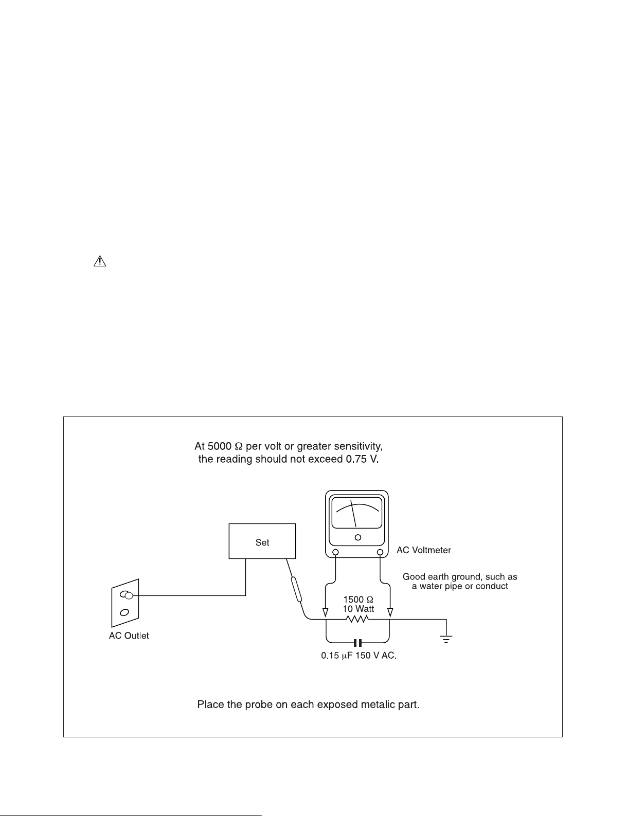
always do an AC leakage current check on the
exposed metal parts of the cabinet, such as
terminals, screw heads, and metal overlays, to
be sure the set is safe to operate danger of
electrical shock. Plug the AC line cord directly
into a 120 V AC outlet(USA Version) or 230 V
AC outlet(EU Version). (Do not use a line
isolation transformer during this check.) Be sure
your AC voltmeter has a sensitivity of 5000 Ω
per volt or greater. Then connect a 1500 Ω 10
watt resistor, paralleled by a 0.15 µF 150 V AC
capacitor, between a known good earth
ground(such as a water pipe, or conduit) and the
exposed metallic parts, one at a time. Measure
the AC voltage across the combination of a 1500
Ω resistor and a 0.15 µF capacitor. Reverse the
AC plug at the AC outlet and repeat AC voltage
measurements for each exposed metalic part.
Voltage measured must not exceed 0.75 V
RMS. This corresponds to 0.2 mA AC. Any
value exceeding this limit constitutes a potential
shock hazard and must be corrected
immediately.
Page 3
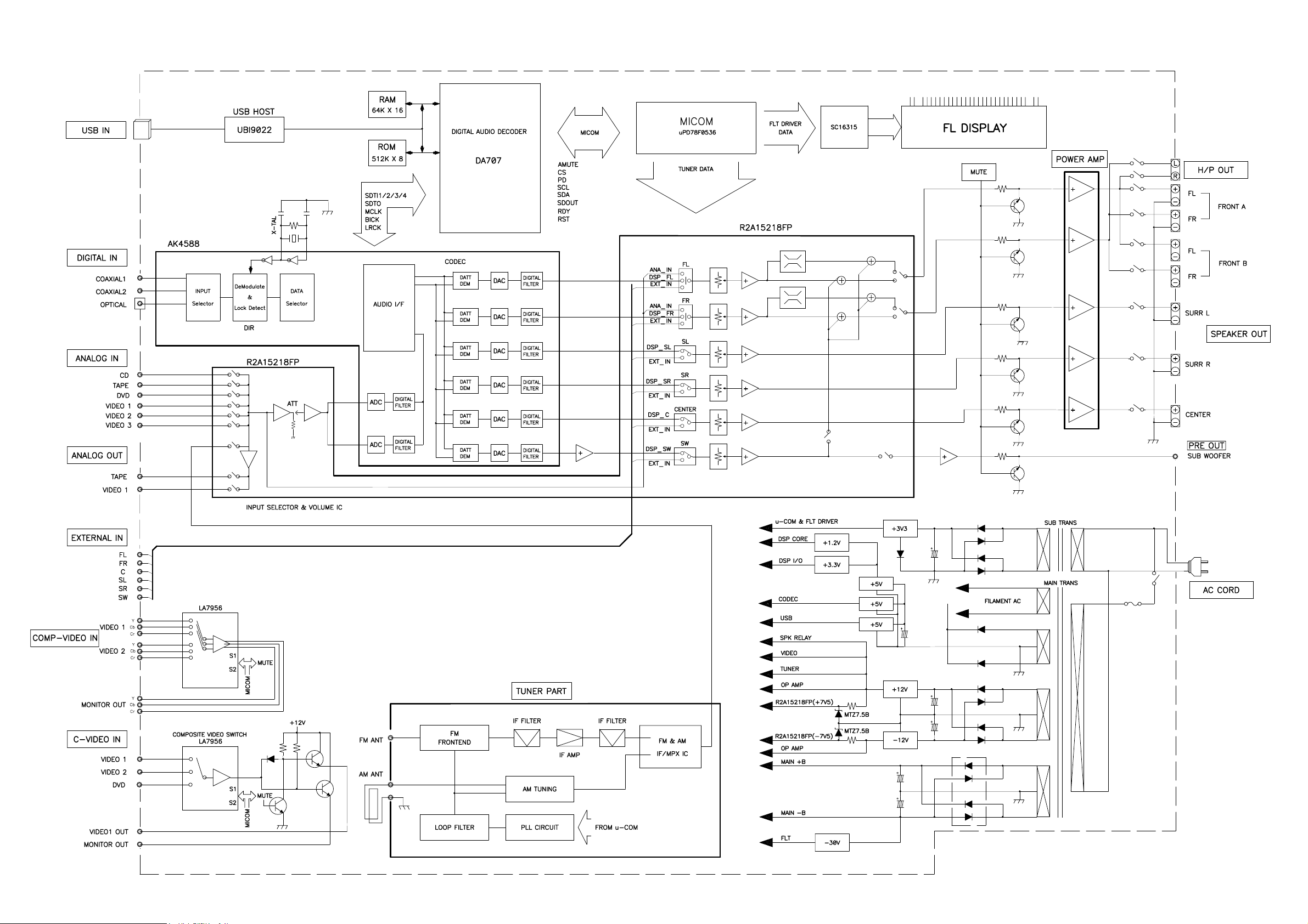
BLOCK DIAGRAM
Model : AVR-133
Page 4
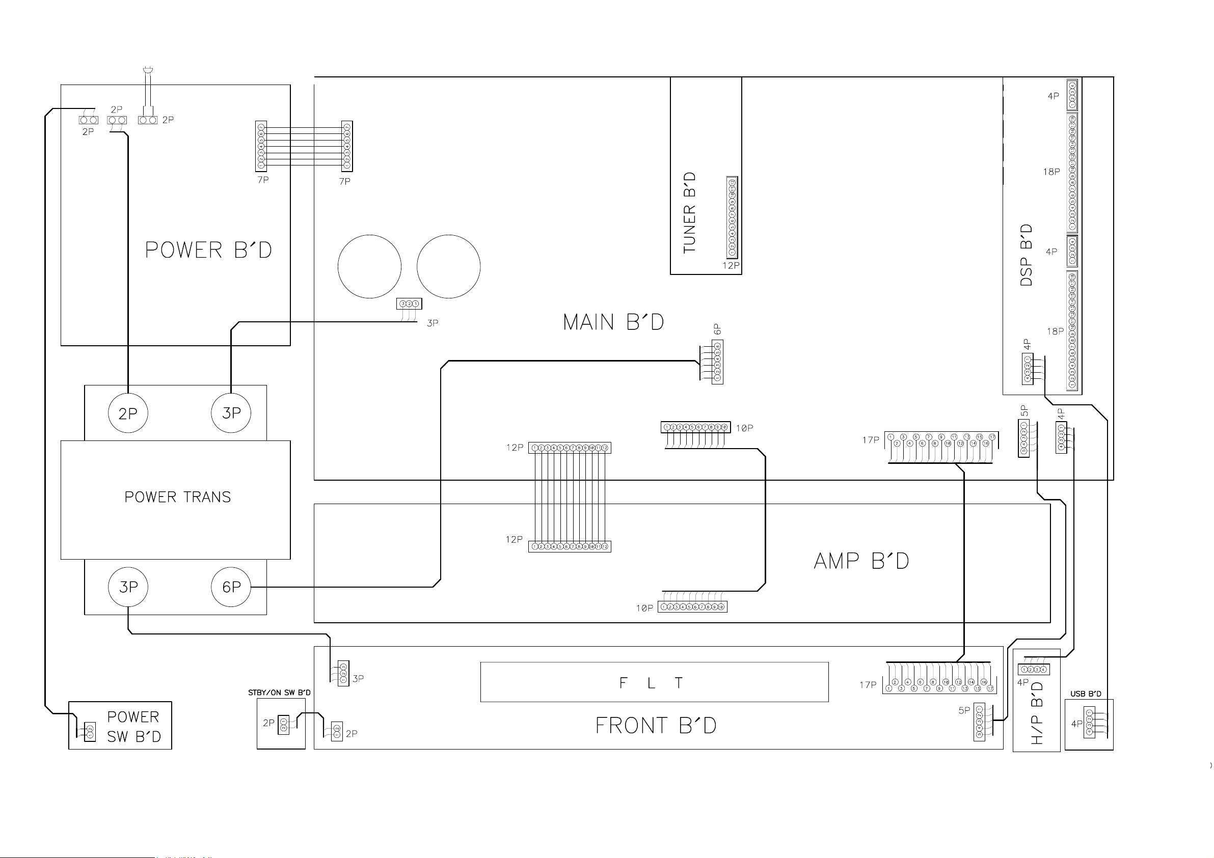
WIRING DIAGRAM
Model : AVR-133
Page 5
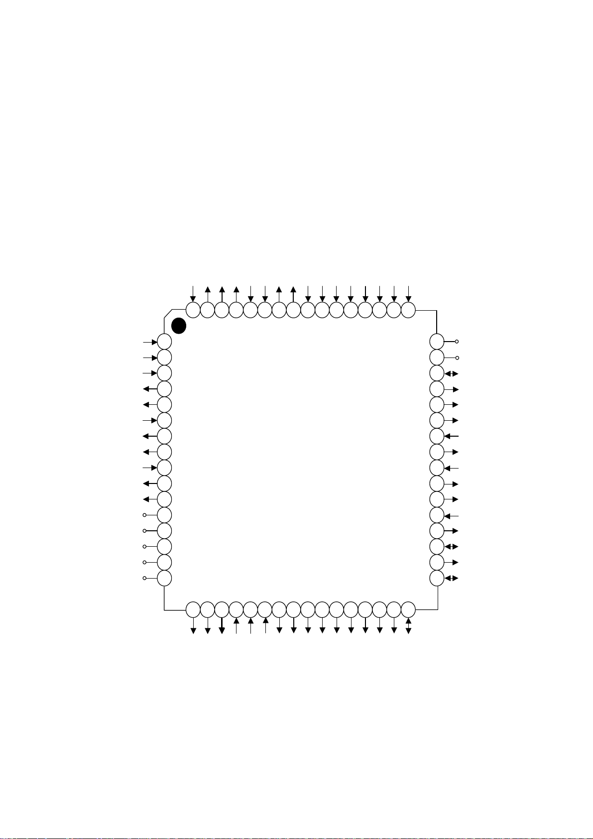
UPD78F0536GK : IC101
(
)
1. Pin Description
POWER_DOWN
64 63 62 61 60 59 58 57 56 55 54 53 52 51 50 49
CIRCUIT DESCRIPTION
FLT/PLL_CLK
FLT/PLL_DATA
FUNC_UP
ST/BY_RLY/FLSW
ST/BY_LED
FLT_CE
RMC
FUNC_DN
HDMI_HPD(NC)
HDMI_S2(NC)
HDMI_S1(NC)
BT/THERMAL_DET
KEY1
KEY3
KEY2
PROTECTION
VOL_UP
VOL_DN
H/P_RLY
C_RLY
RESET
S_RLY
F_RLY
FLMD0
V1OUT_MUTE
TRIG CONTROL
REGC
VSS
EVSS
VDD
EVDD
1 48
2 47
3 46
4 45
5 44
6 43
7 42
8 41
9 40
10 39
11 38
12 37
13 36
14 35
15 34
16 33
17 18 19 20 21 22 23 24 25 26 27 28 29 30 31 32
UPD78F0536
GND
AVREF
24C08_SDA
24C08_SCLK
FRONT B_RLY
TxD
RxD
DSP_RST
DSP_AMUTE
DSP_SDOUT
DSP_CE
DSP_RDY
DSP_PD
DSP/DIR_CDIN
DSP/DIR_CCLK
P31
P32
TUNEND
RDS_CLK
RDS_DATA
VIDEO_S1
VIDEO_S2
VIDEO_MUTE
SW_MUTE
PLL_DO
PLL_CE
C_MUTE
S_MUTE
USB_PC
F_MUTE
R2A15215FP_DATA
R2A15215FP_CLK
Page 6
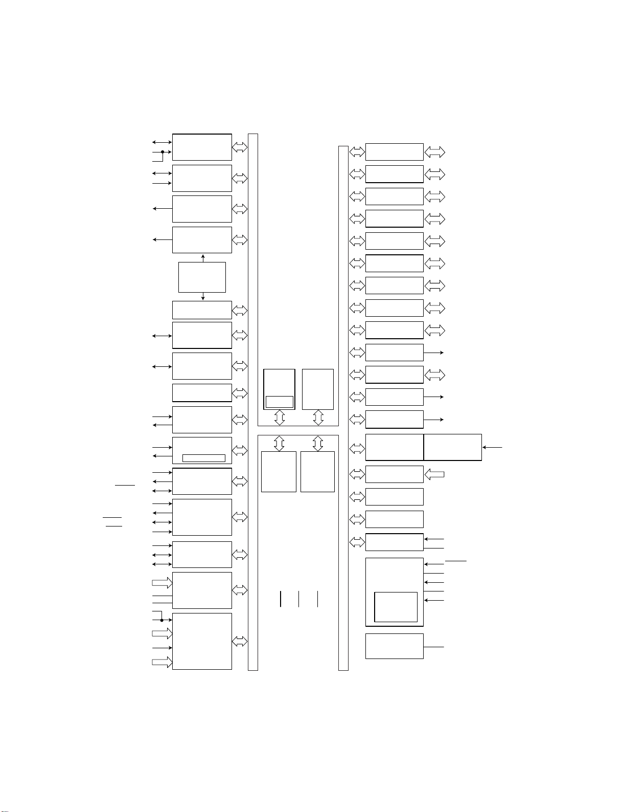
16-bit TIMER/
EVENT COUNTER 00
16-bit TIMER/
EVENT COUNTER 01
TO00/TI010/P01
TI000/P00 (LINSEL)
RxD6/P14 (LINSEL)
TO01
Note 2
/TI011
Note 2
/P06
TI001
Note 2
/P05
TOH0/P15
TOH1/P16
TI50/TO50/P17
TI51/TO51/P33
RxD0/P11
TxD0/P10
RxD6/P14
TxD6/P13
SI10/P11
SO10/P12
SCK10/P10
8-bit TIMER H0
8-bit TIMER H1
WATCHDOG TIMER
WATCH TIMER
INTERNAL
LOW-SPEED
OSCILLATOR
SERIAL
INTERFACE UART0
78K/0
CPU
CORE
BANK
SERIAL
INTERFACE UART6
LINSEL
SERIAL
INTERFACE CSI10
8-bit TIMER/
EVENT COUNTER 50
8-bit TIMER/
EVENT COUNTER 51
SERIAL
INTERFACE IIC0
A/D CONVERTER
SERIAL INTERFACE
CSI11
Notes 1. Available only in the μPD78F0536, 78F0537, and 78F0537D.
2. Available only in the μPD78F0534, 78F0535, 78F0536, 78F0537, and 78F0537D.
3. Available only in the μPD78F0537D.
Note2
Note2
Note1
Note2
Note2
Note3
8
INTERRUPT
CONTROL
2
4
PORT 0
7
P00 to P06
PORT 1
8
P10 to P17
PORT 2
8
P20 to P27
PORT 3
4
P30 to P33
PORT 4
4
P40 to P43
PORT 5
4
P50 to P53
PORT 6
4
P60 to P63
PORT 7
8
P70 to P77
PORT 12
5
P120 to P124
PORT 13
P130
PORT 14
2
P140, P141
BUZZER OUTPUT
BUZ/P141
CLOCK OUTPUT
CONTROL
PCL/P140
KEY RETURN
8
KR0/P70 to
KR7/P77
RESET CONTROL
MULTIPLIER &
DIVIDER
ON-CHIP DEBUG
SYSTEM
CONTROL
INTERNAL
HIGH-SPEED
OSCILLATOR
VOLT AGE
REGULATOR
POWER ON CLEAR/
LOW VOLTAGE
INDICATOR
EXLVI/P120
RESET
REGC
X1/P121
X2/EXCLK/P122
XT1/P123
XT2/EXCLKS/P124
POC/LVI
CONTROL
FLASH
MEMORY
INTERNAL
HIGH-SPEED
RAM
INTERNAL
EXPANSION
RAM
VDD,
EV
DD
VSS,
EV
SS
FLMD0
OCD0A
Note 3
/X1, OCD1A
Note 3
/P31
OCD0B
Note 3
/X2, OCD1A
Note 3
/P32
SI11
Note 2
/P03
SO11
Note 2
/P02
SCK11
Note 2
/P04
SSI11
Note 2
/P05
EXSCL0/P62
SDA0/P61
SCL0/P60
ANI0/P20 to
ANI7/P27
AV
REF
AVSS
RxD6/P14 (LINSEL)
INTP0/P120 (LINSEL)
INTP1/P30 to
INTP4/P33
INTP5/P16
INTP6/P140,
INTP7/P141
2. Block Diagram
Page 7
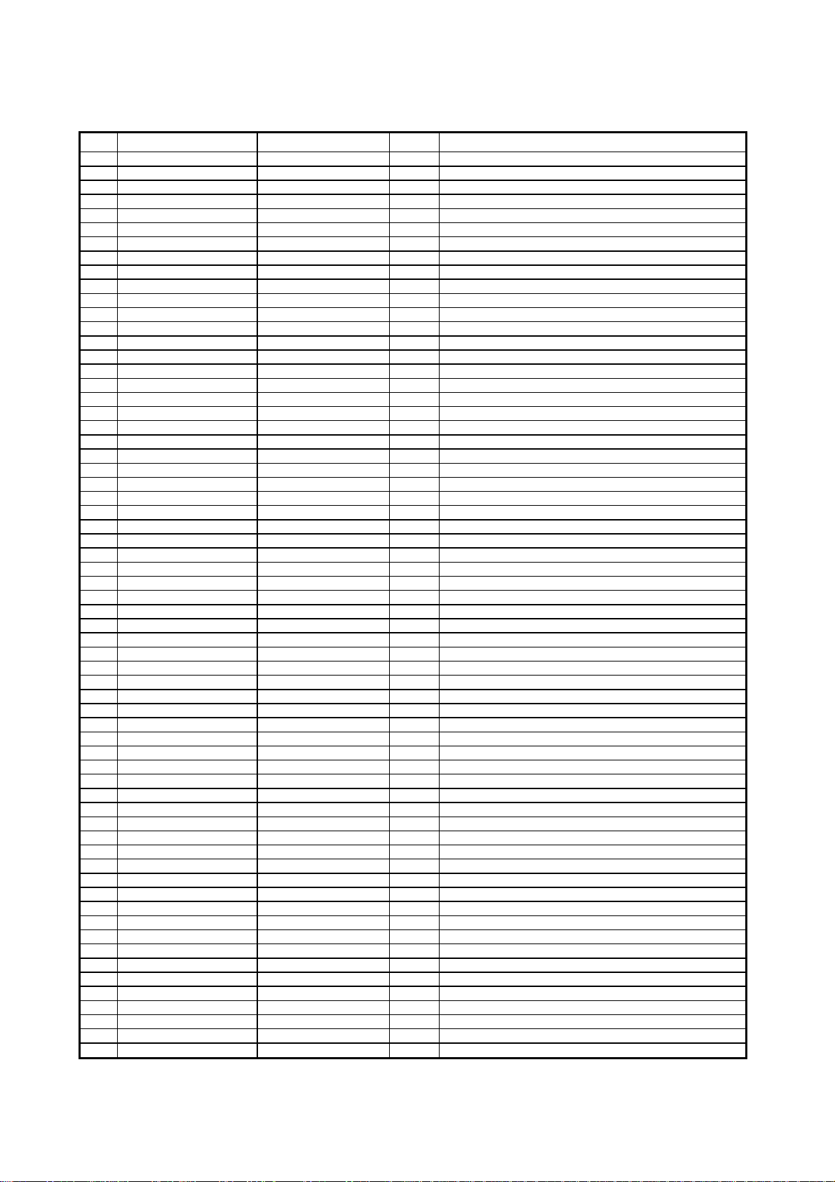
3. Pin Functions
No. Pin Name Pin Symbol I/O Pin Description
1 P120/INTP0/EXLVI PROTECTION I Input for protection
2 P43 VOL_UP I Input for volume up
3 P42 VOL_DN I Input for volume down
4 P41 H/P_RLY O Output for headphone relay
5 P40 C_RLY O Output for center speaker relay
6 RESET RESET I Input for u-com reset
7 P124/XT2/EXCLKS S_RLY O Output for surround speaker relay
8 P123/XT1 F_RLY O Output for front speaker relay
9 IC/FLMD0 FLMD0 O Port for flash mode setting
10 P122/X2/EXCLK V1 OUT_MUTE O Output for VIDEO1 OUT MUTE
11 P121/X1 TRIG CONTROL O Output for DC TRIGGER ON/OFF
12 REGC Connect to ground via 0.47uF/50V E.Cap
13 VSS VSS Ground
14 EVSS EVSS Ground
15 VDD VDD 3V3
16 EVDD EVDD 3V3
17 P60/SCLO VIDEO_MUTE O Output for video mute
18 P61/SDA0 VIDEO_S1/HDMI_S2 O Output for video/HDMI function IC switching
19 P62/EXSCL0 VIDEO_S2/HDMI_S1 O Output for video/HDMI function IC switching
20 P63 TUNED I Input for tuner "TUNED" condition (L is active)
21 P33/TI51/TO51/INTP4 RDS_CLK I Clock signal input from tuner pack
22 P77/KR7 RDS_DATA I Input for RDS data from tuner pack
23 P76/KR6 PLL_CE O Chip select output for tuner pack
24 P75/KR5 PLL_DO O Data output for tuner pack
25 P74/KR4 SW_MUTE O Output for subwoofer channel mute
26 P73/KR3 C_MUTE O Output for center channel mute
27 P72/KR2 S_MUTE O Output for surround channel mute
28 P71/KR1 F_MUTE O Output for front channel mute
29 P70/KR0 USB_PC O Output for IC108(REGULATOR) ON/OFF
30 P06/TI011/TO01 R2A1521FP_CLK O Clock signal output for R2A1521FP
31 P05/TI001/SSI11 R2A1521FP_DATA O Output for R2A1521FP control data
32 P32/INTP3 P32 Port for flash upgrade
33 P31/INTP2 P31 Port for flash upgrade
34 P50 DSP/DIR_CCLK O Clock signal output for DIR/DSP
35 P51 DSP/DIR_CDIN I/O Input & output for DIR/DSP control data
36 P52 DSP_RESET O Output for DSP reset
37 P53 DSP_RDY I Input for DSP enable
38 P30/INTP1 DSP_CE O Chip select output for NJW1153
39 P17/TI50/TO05 DSP_ABOOT O Ouput for DSP Auto boot
40 P16/TOH1/INTP5 DSP_INTREQ I Interrupt signal output to DSP
41 P15/TOH0 DIR_PDN O Output for DIR power down
42 P14/RXD6 RxD I Input for flash upgrade
43 P13/TXD6 TxD O Output for flash upgrade
44 P12/SO10 Front B RLY O Output for SPK B ON/OFF
45 P11/SI10/RXD0 24C08_SCLK O Clock signal output for 24C08
46 P10/SCK10/TXD0 24C08_SDA I/O Input & output for 24C08 control data
47 AVREF AVREF 3V3
48 AVSS AVSS GROUND
49 P27/ANI7 KEY2 I Input for KEY2 scan
50 P26/ANI6 KEY3 I Input for KEY3 scan
51 P25/ANI5 KEY1 I Input for KEY1 scan
52 P24/ANI4 BT/THERMAL_DET I BLUETOOTH DETECT
53 P23/ANI3 HDMI_HPD O Ouput for HDMI HPD(NOT USED)
54 P22/ANI2 HDMI_S2 O Ouput for HDMI S2 CONTROL(NOT USED)
55 P21/ANI1 HDMI_S2 O Ouput for HDMI S1 CONTROL(NOT USED)
56 P20/ANI0 FUNC_DN I Input for function encoder down
57 P130 ST/BY_LED O Ouput for standby led
58 P04/SCK11 ST/BY_RLY O Onput for standby relay
59 P03/S111 FUNC_UP I Input for function encoder up
60 P02/S011 FLT/PLL_DATA O Output for FLT/PLL control data
61 P01/TI010/TO00 FLT/PLL_CLK O Clock signal output for FLT/PLL
62 P00/TI000 RMC I Input for remocon data
63 P141/BUZ/INTP7 FLT_CE O Chip select output for FLT
64 P140/PCL/INTP6 POWER_DOWN I Input for power down
Page 8
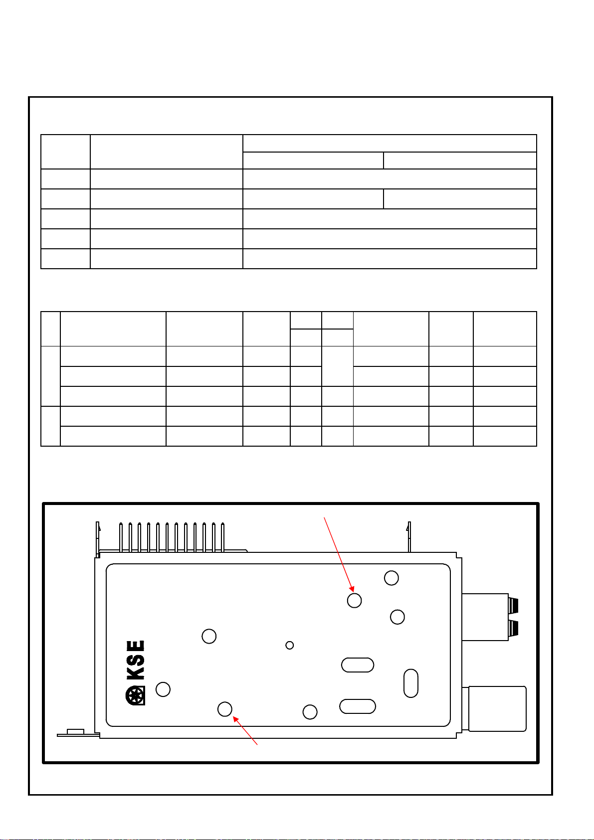
ALIGNMENT PROCEDURES
1.Electrical specification.
1.Electrical specification.
1.Electrical specification.1.Electrical specification.
NO.
NO.
NO.NO.
ITEMS
ITEMS
ITEMSITEMS
SPECIFICATION
SPECIFICATION
SPECIFICATIONSPECIFICATION
M W F M
1-1
1-2
1-3
1-4
1-5
2.Electrical Characteristics.
2.Electrical Characteristics.
2.Electrical Characteristics.2.Electrical Characteristics.
NO
AF Output Level
FM
Auto Stop Level
Stereo Separation 1kHz
AF Output Level
MW
Auto Stop Level
Local OSC
Frequency cover range
Standard supply voltage
FM Antenna input Impedance
AM Loop Antenna
TEST ITEMS
TEST
CONDITION
47• Load 98.1 60
47• Load 999 74
Above the receiving Frequency
522 ~1620kHz 87.5 ~ 108.0MHz
12.0(±0.5V)
75 ohm
9.5uH ( 1kHz ) : S0160BL-25
T.P.
98.1 --
98.1 60
999
MOD.T.L.
kHz,%dBu
280±100 mV
40
25 ±6 dBu
25 min dB
30 180 ±60
--
UNITSpecification
mV Non Adjust
dBu
Adjustment
Non Adjust
SVR01
SVR02
Non Adjust30 55 ±15
3.Adjust Point.
3.Adjust Point.
3.Adjust Point.3.Adjust Point.
FM STEREO SEPARATION Adj.
SVR02
SVR01
FM AUTO STOP LEVEL Adj.
<KST-MU004MV1-0 Adj POINT>
<KST-MU004MV1-0 Adj POINT>
<KST-MU004MV1-0 Adj POINT><KST-MU004MV1-0 Adj POINT>
Page 9
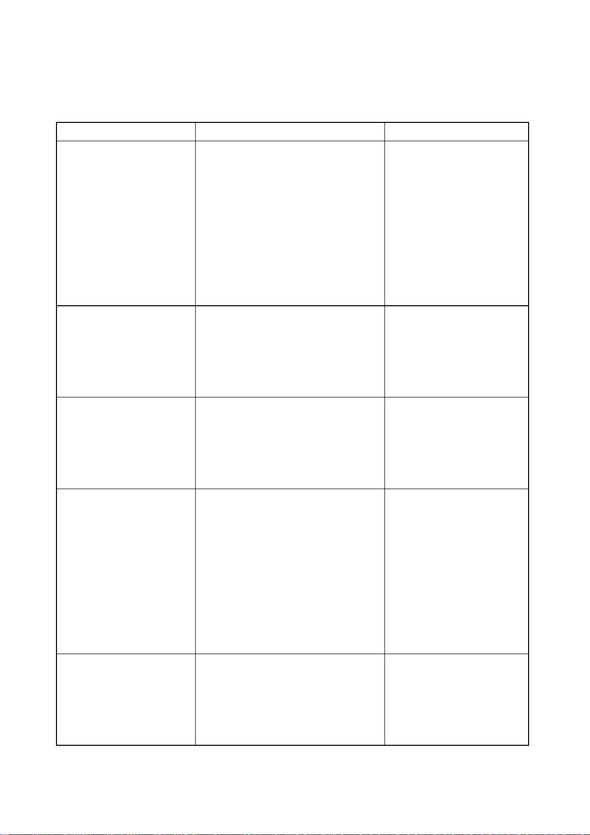
TROUBLESHOOTING
Cause and RemedySymptom
Power On Failure A) AC-Cord check.
1. FLT does not light up. B) Power Trans (Main/ST-BY) check.
2. ST-BY LED does not light up. C) Fuse's disconnection check. F ( 301)
D) Connector's disconnection or disjunction.
Change or close insertion of the connector. CN301,FPC101
E) Inferior ST-By switch. SW(700)
F) VFD Driver I.C & Resonator check. I.C701 SC16315
1. VFD Driver I.C VCC(+3.3)V check. I.C701 Pin No13
2. VFD Driver clock pulse check. I.C701 Pin No5
Fuse Disconnection. A) Inferior transformer.
(Power On) B) AMP drive TR out. (POWER TR) Q206( FL, FR, C, SL, SR )
C) AMP drive TR out. ( POWER TR ) Q205 ( FL, FR, C, SL, SR )
D) voltage check.
1. B+ ( 47 )V, B- ( 47 ) V
Key Disorder. A) Key's being pushed check.
Ref No.
B) Key signal input components inferior.
C) Key PORT check. I.C101 Pin No. (49,50,51 )
D) µ-COM I.C inferior.
1. µ-COM IC VCC +3.3V check. I.C101 Pin No. ( 15,16,47 )
Power Off in 2~3 sec. A) Regulator I.C out. I.C 300 (LM1117S_3.3V)
after Power On. 1. Signal IN/OUT check.
B) Drive transistor out. ( POWER TR ) Q205 ( FL, FR, C, SL, SR )
Q206( FL, FR, C, SL, SR )
C) Protection circuit check.
1. Output DC check.
2. µ-COM I.C protection terminal check. u-COM Pin No. ( 1 )
D) Connector's disconnection or disjunction CP (111)
E) SLEEP MODE cancellation.
Bump Sound A) FRONT Mute transistor's out and inferior. Q (105 )
(During input-select switch's change.) µ-Com front mute control PORT check. IC101 Pin No. ( 28 )
B) CENTER Mute transistor's out and inferior. Q ( 107 )
µ-Com center mute control PORT check. IC101 Pin No. ( 26 )
C) SURROUND Mute transistor's out and inferior.
Q ( 109 )
Page 10
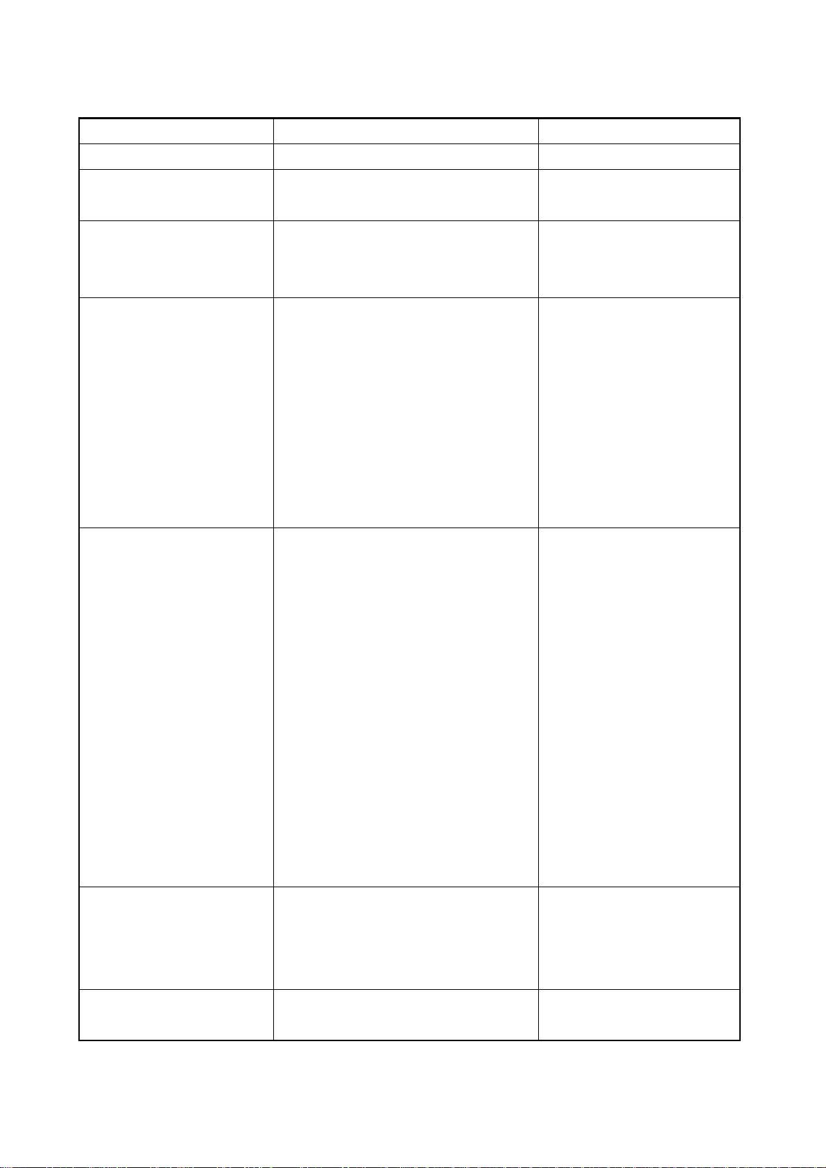
Cause and RemedySymptom
µ-Com surround mute control PORT check. IC101 Pin No. ( 27 )
Sounds from Speaker when A) NOT Supported Headphone Detect.
Headphone's connected. Push the Speaker On/Off Button(Speaker off).
Bass / Treble Control Failure. A) Volume IC check. I.C109
1. Resister/Capacitor correction figure check.(Bass) I.C109 PIN No. ( 26,27,32,33)
2. Resister/Capacitor correction figure check.(Treble) I.C109 PIN No. ( 28,34)
AMP Sound Dead. A) Signal Mute TR's inferior. Q 105,107,109
1. "LEFT" Channel dead. B) Connector disconnection & disjunction. CP ( 111)
2. "RIGHT" Channel dead. Change or close insertion of the connector.
3. "CENTER" Channel dead. C) Speaker wire's disjunction.
4. "REAR" Channel dead. Close insertion of the speaker wire.
D) Volume IC check. I.C No. ( 109 )
1. I.C voltage check ( +7.5 )V, ( -7.5 )V I.C Pin No. ( 30,52)
2. I.C control data check. I.C PIN No. (49,50)
3. I.C signal IN/OUT check.
Ref No.
AC-3/DTS Failure. A) I.C Regulator check.
(DSP Sound Mode) DSP I/O + (3.3)V,DSP CORE + (1.2)V REG101,REG102
CODEC + ( 5)V,CODEC + ( 3.3)V I.C No. (112 ), REG100
B) DIR check. I.C103
1. OSC check. X-TAL ( 100 )
2. BICK, LRCK, RDATA Check. I.C Pin No. ( 15) ( 16 ) ( 14 )
3. Micom Interface Port Check. I.C Pin No. ( 21,22,31 )
C) DSP Check. I.C No. ( 102)
1. LRCK Check. I.C Pin No. ( 12 )
2. Micom Interface Port Check. I.C Pin No.(3,4,14,105,107,108,110,111)
3. SDATA 1, 2, 3,4 Check. I.C Pin No. ( 117,116,115,113)
D) D/A Check. I.C No. ( 103)
1. LRCK/BCK/SDATA check. I.C Pin No. ( 17,18,19)
2. Signal out check. I.C Pin No. ( 49,47,45,43,41,39,37,35 )
Video Output Dead. A) Video Regulator voltage check.
1. DC voltage check. + ( 12 )V I.C No. ( 106)
B) Micom control data check. I.C Pin No. ( 2,3 )
C) Video Mute(MONTOR,V1 OUT) port check.(IC101) I.C Pin No. ( 17,10)
Remote Controller Failure. A) Battery check.
B) RMC I.C & Resonator inferior.
Page 11
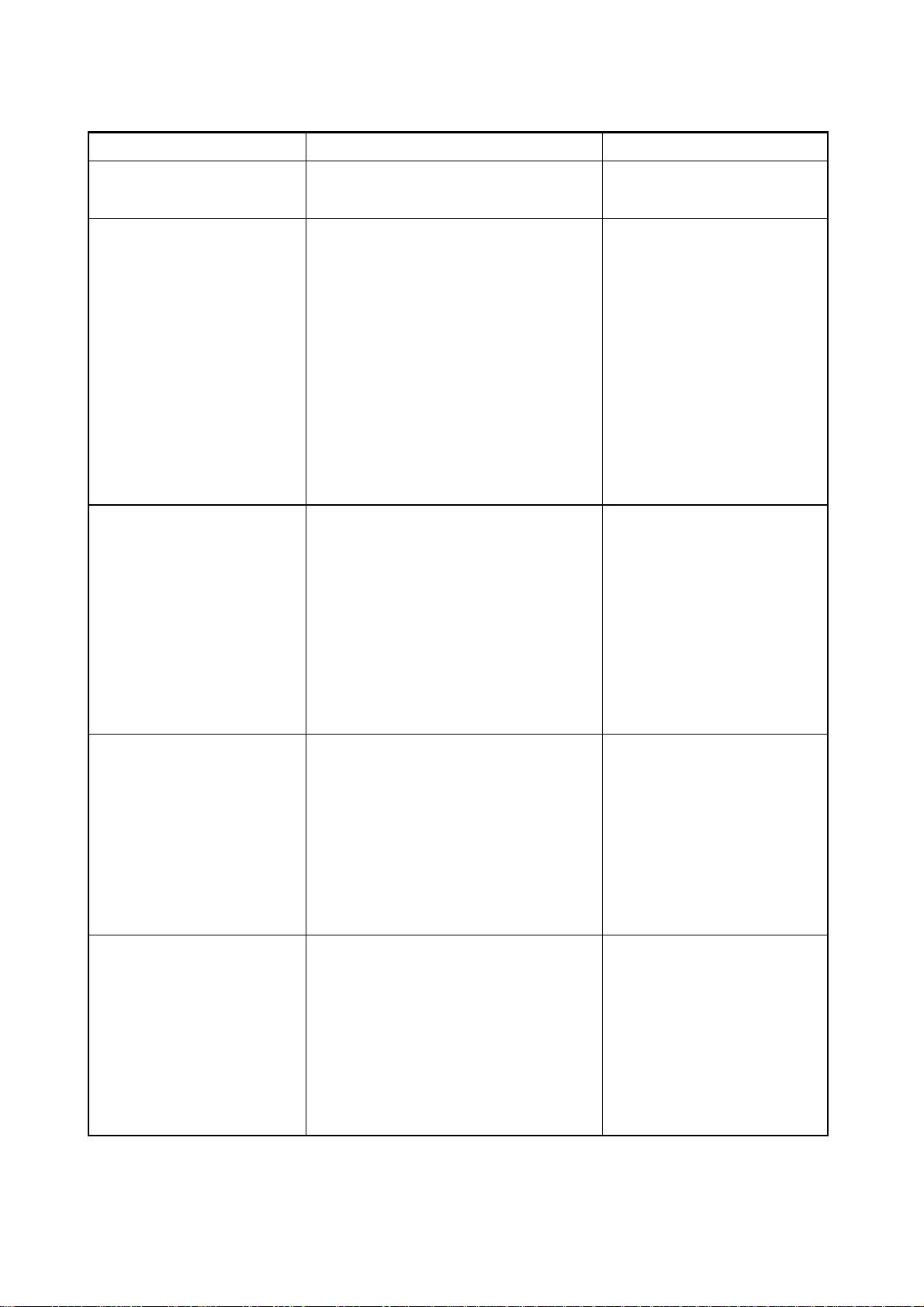
Cause and RemedySymptom
1. µ-COM I.C B+( 3.3 )V check.
2. REMOCON data check. I.C NO. (101) / I.C Pin No. ( 62)
FM Failure. A) FM MUTE adjustment inferior.
B) FRONT-END inferior.
C) FM DET COIL inferior.
D) PLL&MPX IC check.
1. PLL&MPX I.C B+( 5 )V,B+( 3.3 )V check. I.C NO. (1 ) / I.C Pin No. ( 8,21 )
2. PLL control data check. (Data/CE/Clock)
E) TUNER B+ voltage inferior.
F) µ-COM I.C & Resonator inferior. I.C No. ( 101 )
1. µ-COM I.C B+( 3.3 )V check.
2. Micom control data check. I.C Pin No. ( 20,23,24,60,61)
AM Failure. A) PLL&MPX IC check.
1. PLL&MPX I.C B+( 5 )V,B+( 3.3 )V check. I.C NO. (1 ) / I.C Pin No. ( 8,21 )
2. PLL control data check (Data/CE/Clock)
Ref No.
B) TUNER B+ voltage inferior.
C) AM OSC COIL inferior.
D) µ-COM I.C & Resonator inferior. I.C No. (101 )
1. µ-COM I.C B+( 3.3)V check.
2. Micom control data check. I.C Pin No. ( 20,23,24,60,61)
Stereo Effect Failure. A) FM DET COIL Inferior.
Stereo does not light up. B) PLL&MPX IC check.
1. PLL&MPX I.C B+( 5 )V,B+( 3.3 )V check.
2. MPX control data check.
C) µ-COM I.C & Resonator inferior. I.C No. ( 101 )
1. µ-COM IC B+( 3.3)V check
2. Micom control data check. I.C Pin No. ( 20,23,24,60,61)
Tuner Sound Dead. A) Connector's disconnection or disjunction.
1. "L / R" Channel dead. Change or Close insertion of the connector.
2. "LEFT" Channel dead. B) FM DET COIL inferior.
3. "RIGHT" Channel dead. C) AM IFT COIL inferior.
D) PLL&MPX IC check.
1. Signal IN/OUT terminal.
2. I.C driving voltage check. ( +5V,+3V3 ) I.C NO. (1 ) / I.C Pin No. ( 8,21 )
Page 12
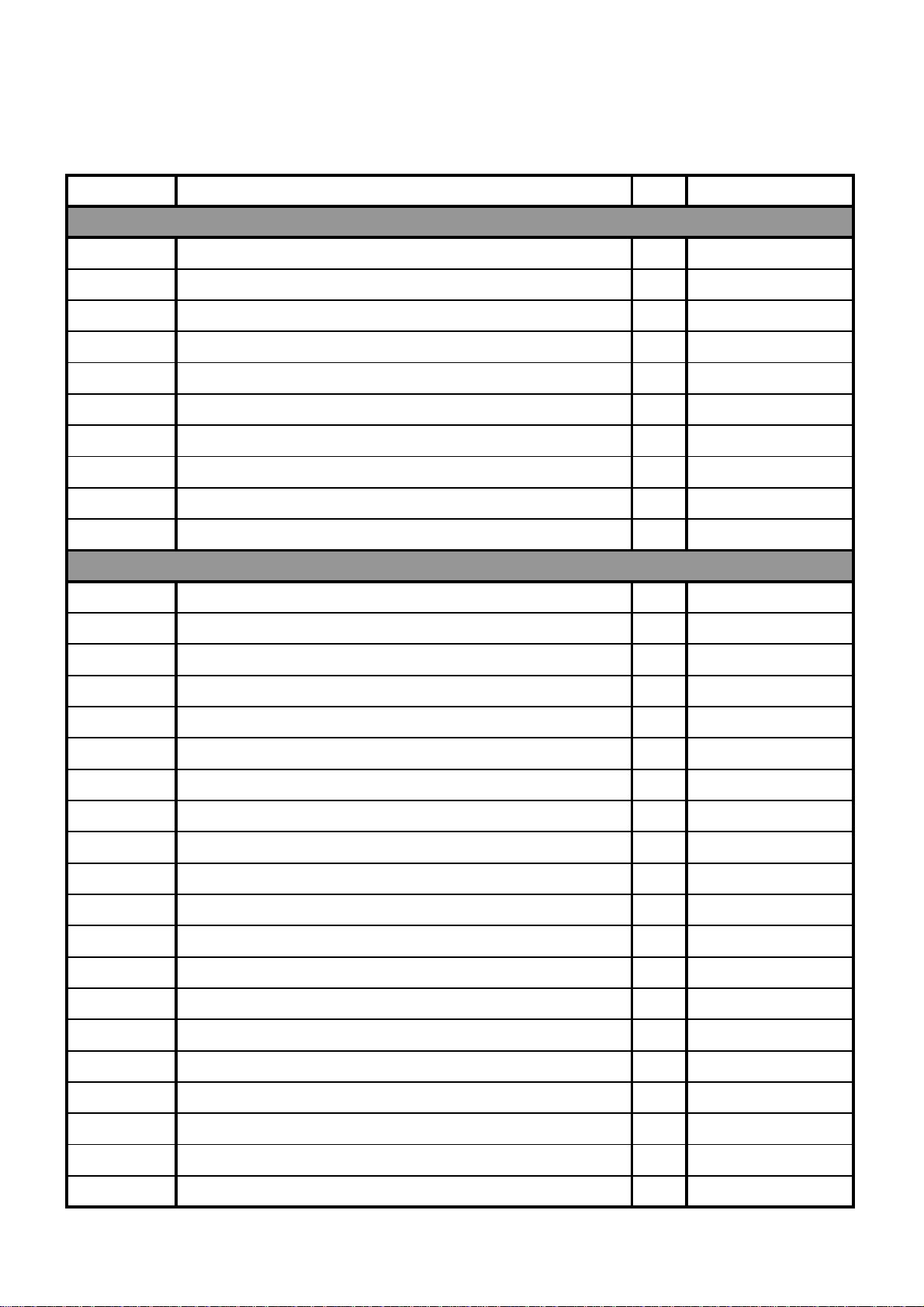
★ MECHANICAL PARTS LIST ( AVR-133
)
♣ Parts without Parts No. are not supplied.
No. DESCRIPTION Q'TY PARTS No.
PACKAGE
INSTRUCTION MANUAL 1 5707000001360S
BOX,GIFT(535*448*235) 1 6007211180010S
CUSHION,SNOW(EPS) 2 6230212064000S
PE,SHEET 750*1460/SET 1 6327040059000S
POLY BAG, 330*240*0.05 1 6337040062010S
POLY BAG, 85*70 1 6337210242000S
REMOCON 1 8300310000010S
ANTENNA, LOOP 1 E601016000010S
ANTENNA, WIRE(FM) 1 E605010070001S
BATTERY, AAA 3 G670001R50210S
CABINET & CHASSIS
1 WINDOW, DISPLAY 1 5077212543000S
2 FILTER, FLT 1 5200210262000S
3 BADGE 1 5630210548000S
4 PANEL, FRONT 1 3067213971000S
5 FELT, STRIP 2 2690040057010S
6 LENS, STANDBY 1 3710210793000S
7 BUTTON, STANDBY 1 5097213641000S
8 BUTTON, POWER SWITCH 1 5097213631000S
9 PCB ASS'Y, STANDBY SW 1
10 BRACKET, POWER SWITCH 1 4010213546000S
11 SW, PUSH 1 G000122006060S
12 PCB ASS'Y, POWER SW 1
13 PCB ASS'Y, FRONT 1
14 HEAT SINK, MAIN 1 2120210538100S
15 PCB ASS'Y, GUIDE1 1
16 BRACKET, H SINK 5 4010056906010S
17 CABINET, TOP 1 3007041236061S
18 PCB ASS'Y, AMP 1
19 CHASSIS, MAIN 1 3200200026020S
20 POWER TRANS, 240V/50HZ 1 8200858630220S
Page 13
No. DESCRIPTION Q'TY PARTS No.
21 CUSHION, 12tX30X15 1 4050044345010S
22 PCB ASS'Y, STANDBY 1
23 PLATE, KNOB 1 4470211422000S
24 KNOB, CAP 1 5087211781000S
25 BUSHING, SHAFT 1 2410210061000S
26 KNOB, VOLUME 1 5080211793000S
27 PLATE, PANEL 1 4470211432000S
28 CN,PLUG CONTACT(USB) 1 G480040100010S
29 PCB ASS'Y, USB 1
30 SHIELD, PLATE USB 1 3070210456000S
31 BUTTON, FUNCTION 1 5097213651000S
32 SW, ENCODER 1 G121123070020S
33 TER,RCA 3PIN 1 G606040320020S
34 SHIELD, PLATE VIDEO 1 3070210466000S
35 PCB ASS'Y, GUIDE3 1
36 PCB ASS'Y, GUIDE2 1
37 FOOT, TITAN 2 4007040201060S
38 PCB ASS'Y, MAIN 1
39 HEAT SINK, H=45/REG TR 1 2120043538030S
40 HEAT SINK, REG TR(24X45) 1 2120044298010S
41 PCB ASS'Y, DSP 1
42 MODULE, JSR1165-C /OPTICAL 1 E100116500040S
43 TER,RCA 2PIN 1 G601206A0200YS
44 SHIELD, PLATE DSP 1 3070210476000S
45 TER,RCA 12PIN 1 G6081201A120YS
46 TER,RCA 3PIN 1 G60631901B20YS
47 TER,RCA 6PIN 1 G603610A0041YS
48 TUNER, FM/AM 1 E903004100010S
49 TER,RCA 3PIN 1 G606305A1400YS
50 TER,RCA 2PIN 1 G601207BE050YS
51 TER,RCA 9PIN 1 G6070902C016YS
52 PCB ASS'Y, COMPONENT 1
53 FOOT, PL 2 4000040201010S
54 TER,BOARD PUSH 8P 1 G598801SA090YS
55 TER,BOARD PUSH 6P 1 G596601SA090YS
Page 14
No. DESCRIPTION Q'TY PARTS No.
56 CHASSIS, BACK 1 3207212506000S
57 SOCKET,POWER AC 1 G430040550010S
58 JACK,D6.5 1 G402PJ619A01YS
59 PCB ASS'Y, HEADPHONE 1
60 DISPLAY, FLT 1 K530080300010S
61 HOLDER, FLT 1 432004078301AS
62 POSISTOR 1 F320161020240S
SCREWS
S1 SCREW, +2S 4*8 B-TYPE(DOT) BK/BH 4 1500040083B10S
S2 SCREW, +2S 3*10 B-TYPE(DOT) BK/BH 30 B020030103B11S
S3 SCREW, 3X18 B-TYPE ZNW/BH 5 B020030181B10S
S4 SCREW, +3S 4*10 P+S-WASHER ZNW/BH 4 B028940101B10S
S5 SCREW, +2S 3*16+S-WASHER ZNW/HH 15 1507041146010S
S6 SCREW, +2S 3*8 ZnY WASHER PI12 2 1500001456010S
S7 SCREW, +2S 3*8 B-TYPE ZNW/BH 46 B020030081B10S
S8 SCREW, +2S 3*8 B-TYPE BK/BH 7 B020030083B10S
MISCELLANEOUS
Q206C KTB2510, PNP 1 J501251000010S
Q206FL KTB2510, PNP 1 J501251000010S
Q206FR KTB2510, PNP 1 J501251000010S
Q206SL KTB2510, PNP 1 J501251000010S
Q206SR KTB2510, PNP 1 J501251000010S
Q205C KTD1510, NPN 1 J503151000020S
Q205FL KTD1510, NPN 1 J503151000020S
Q205FR KTD1510, NPN 1 J503151000020S
Q205SL KTD1510, NPN 1 J503151000020S
Q205SR KTD1510, NPN 1 J503151000020S
Q204C 2SD947F, NPN 1 J503947F00000S
Q204FL 2SD947F, NPN 1 J503947F00000S
Q204FR 2SD947F, NPN 1 J503947F00000S
Q204SL 2SD947F, NPN 1 J503947F00000S
Q204SR 2SD947F, NPN 1 J503947F00000S
CN,WIRE 100MM (2P) 1 L000101020240S
CORD ASS'Y, 16A/250V 1 L068250160020S
CABLE,FLAT CARD 1.25MM 1 N712172234810S
Page 15

EXPLODED VIEW
Model : AVR-133
Page 16

★ ELECTRICAL PARTS LIST (AVR-133
)
♣ Parts without Parts No. are not supplied.
REF No. Q'TY PARTS No.
ASSEMBLY P.C.BOARD MAIN 7025HK0805010
COILS
BD103/BD104 BEAD COIL, 120ohm 2 D340160811210S
BD106-BD110 BEAD COIL, 120ohm 5 D340160811210S
BD113-BD115 BEAD COIL, 120ohm 3 D340160811210S
BD116-BD119 FILTER COIL, BFS2550A0F1 4 D320255000520S
CAPACITORS
C101L/R CERAMIC CHIP T.C 100 pF 50V J 2 D010101167160S
C102L/R ELECT GE 85C 10 uF 50V M 2 D040100087070S
C103L/R CERAMIC CHIP T.C 100 pF 50V J 2 D010101167160S
C104L/R ELECT GE 85C 10 uF 50V M 2 D040100087070S
C105L/R CERAMIC CHIP T.C 220 pF 50V J 2 D010221167160S
C106L/R ELECT GE 85C 10 uF 50V M 2 D040100087070S
C107L/R CERAMIC CHIP T.C 220 pF 50V J 2 D010221167160S
C108L/R ELECT GE 85C 10 uF 50V M 2 D040100087070S
C109L/R CERAMIC CHIP T.C 220 pF 50V J 2 D010221167160S
C110L/R ELECT GE 85C 10 uF 50V M 2 D040100087070S
C111L/R CERAMIC CHIP T.C 220 pF 50V J 2 D010221167160S
C112L/R ELECT GE 85C 10 uF 50V M 2 D040100087070S
C113L/R CERAMIC CHIP T.C 220 pF 50V J 2 D010221167160S
C114L/R ELECT GE 85C 10 uF 50V M 2 D040100087070S
C115C CERAMIC CHIP T.C 100 pF 50V J 1 D010101167160S
C115L/R CERAMIC CHIP T.C 100 pF 50V J 2 D010101167160S
C115SL CERAMIC CHIP T.C 100 pF 50V J 1 D010101167160S
C115SR CERAMIC CHIP T.C 100 pF 50V J 1 D010101167160S
C115SW CERAMIC CHIP T.C 100 pF 50V J 1 D010101167160S
C116C ELECT GE 85C 10 uF 50V M 1 D040100087070S
C116L/R ELECT GE 85C 10 uF 50V M 2 D040100087070S
C116SL ELECT GE 85C 10 uF 50V M 1 D040100087070S
C116SR ELECT GE 85C 10 uF 50V M 1 D040100087070S
C116SW ELECT GE 85C 10 uF 50V M 1 D040100087070S
C117L/R ELECT GE 85C 10 uF 50V M 2 D040100087070S
C118/C119 ELECT GE 85C 10 uF 50V M 2 D040100087070S
C120 CERAMIC CHIP HIK 0.022 uF 25V K 1 D011223777160S
C121 CERAMIC CHIP HIK 0.047 uF 16V K 1 D011473773160S
C122 CERAMIC CHIP HIK 0.15 uF 10V Z 1 D011154792160S
C123-C128 ELECT GE 85C 100 uF 10V M 6 D040101082090S
C131 ELECT GE 85C 47 uF 10V M 1 D040470083080S
C132 CERAMIC CHIP HIK 0.15 uF 10V Z 1 D011154792160S
C133 CERAMIC CHIP HIK 0.047 uF 16V K 1 D011473773160S
C134 CERAMIC CHIP HIK 0.022 uF 25V K 1 D011223777160S
C135 CERAMIC CHIP T.C 0.01 uF 16V K 1 D010103777160S
C1366 CERAMIC CHIP T.C 0.01 uF 16V K 1 D010103777160S
C137/C138 CERAMIC CHIP T.C 100 pF 50V J 2 D010101167160S
C139 ELECT GE 85C 47 uF 10V M 1 D040470083080S
C140SW ELECT GE 85C 10 uF 50V M 1 D040100087070S
C141SW CERAMIC CHIP T.C 0.01 uF 16V K 1 D010103777160S
C142SW CERAMIC CHIP HIK 1000 pF 50V K 1 D011102777160S
C143SW CERAMIC CHIP T.C 47 pF 50V J 1 D010470167160S
DESCRIPTION
Page 17

REF No. Q'TY PARTS No.
DESCRIPTION
C144SW CERAMIC CHIP T.C 0.01 uF 16V K 1 D010103777160S
C145SW ELECT GE 85C 47 uF 10V M 1 D040470083080S
C146SW ELECT GE 85C 47 uF 10V M 1 D040470083080S
C147SW CERAMIC CHIP HIK 3300 pF 50V K 1 D011332777160S
C149SW ELECT GE 85C 10 uF 50V M 1 D040100087070S
C150SW CERAMIC CHIP T.C 330 pF 50V J 1 D010331167160S
C151SW CERAMIC CHIP T.C 680 pF 50V J 1 D010681167160S
C154C CERAMIC CHIP HIK 3300 pF 50V K 1 D011332777160S
C154L/R CERAMIC CHIP HIK 3300 pF 50V K 2 D011332777160S
C154SL CERAMIC CHIP HIK 3300 pF 50V K 1 D011332777160S
C154SR CERAMIC CHIP HIK 3300 pF 50V K 1 D011332777160S
C158C ELECT GE 85C 4.7 uF 50V M 1 D0404R7087250S
C158L/R ELECT GE 85C 4.7 uF 50V M 2 D0404R7087250S
C158SL ELECT GE 85C 4.7 uF 50V M 1 D0404R7087250S
C158SR ELECT GE 85C 4.7 uF 50V M 1 D0404R7087250S
C158SW ELECT GE 85C 10 uF 50V M 1 D040100087070S
C159C CERAMIC CHIP T.C 0.01 uF 16V K 1 D010103777160S
C159F CERAMIC CHIP T.C 0.01 uF 16V K 1 D010103777160S
C159S CERAMIC CHIP T.C 0.01 uF 16V K 1 D010103777160S
C159SW CERAMIC CHIP T.C 0.01 uF 16V K 1 D010103777160S
C160C FILM POLYESTER 0.1 uF 100V J 1 D02010406C060S
C160L/R FILM POLYESTER 0.1 uF 100V J 2 D02010406C060S
C160SL FILM POLYESTER 0.1 uF 100V J 1 D02010406C060S
C160SR FILM POLYESTER 0.1 uF 100V J 1 D02010406C060S
C161C FILM POLYESTER 0.01 uF 100V J 1 D02010306C060S
C161L FILM POLYESTER 0.01 uF 100V J 1 D02010306C060S
C161L1 FILM POLYESTER 0.01 uF 100V J 1 D02010306C060S
C161R FILM POLYESTER 0.01 uF 100V J 1 D02010306C060S
C161R1 FILM POLYESTER 0.01 uF 100V J 1 D02010306C060S
C161SL FILM POLYESTER 0.01 uF 100V J 1 D02010306C060S
C161SR FILM POLYESTER 0.01 uF 100V J 1 D02010306C060S
C162C FILM POLYESTER 0.01 uF 100V J 1 D02010306C060S
C162L/R FILM POLYESTER 0.01 uF 100V J 2 D02010306C060S
C162SL FILM POLYESTER 0.01 uF 100V J 1 D02010306C060S
C162SR FILM POLYESTER 0.01 uF 100V J 1 D02010306C060S
C164SW CERAMIC CHIP T.C 100 pF 50V J 1 D010101167160S
C165L/R FILM POLYESTER 0.01 uF 100V J 2 D02010306C060S
C167 ELECT GE 85C 2.2 uF 50V M 1 D0402R2087160S
C168-C170 CERAMIC CHIP T.C 0.01 uF 16V K 3 D010103777160S
C171-C174 CERAMIC CHIP T.C 100 pF 50V J 4 D010101167160S
C175 ELECT GE 85C 47 uF 10V M 1 D040470083080S
C176 ELECT GE 85C 10 uF 50V M 1 D040100087070S
C178 ELECT GE 85C 10 uF 50V M 1 D040100087070S
C179/C180 ELECT GE 85C 10000 uF 63V M 2 D040103088380S
C182-C186 FILM POLYESTER 0.1 uF 250V K 5 D02010407H080S
C187/C188 ELECT GE 85C 1 uF 50V M 2 D040010087150S
C189 ELECT GE 85C 330 uF 63V M 1 D040331088230S
C190 ELECT GE 85C 4.7 uF 100V M 1 D0404R708C060S
C191 ELECT GE 85C 10 uF 50V M 1 D040100087070S
C192 CERAMIC CHIP HIK 0.1 uF 50V K 1 D011104577160S
C193 ELECT GE 85C 330 uF 10V M 1 D040331082070S
C194 CERAMIC CHIP HIK 0.1 uF 50V K 1 D011104577160S
C195 ELECT GE 85C 330 uF 10V M 1 D040331082070S
Page 18

REF No. Q'TY PARTS No.
DESCRIPTION
C196 CERAMIC CHIP HIK 0.1 uF 50V K 1 D011104577160S
C197 ELECT GE 85C 100 uF 10V M 1 D040101082090S
C198/C199 CERAMIC CHIP HIK 0.1 uF 50V K 2 D011104577160S
C200 ELECT GE 85C 6800 uF 16V M 1 D040682083000S
C201-C203 FILM POLYESTER 0.1 uF 100V J 3 D02010406C060S
C204/C205 ELECT GE 85C 1 uF 50V M 2 D040010087150S
C206 ELECT GE 85C 4700 uF 25V M 1 D040472084020S
C207 ELECT GE 85C 1000 uF 25V M 1 D040102084060S
C208-C210 FILM POLYESTER 0.1 uF 100V J 3 D02010406C060S
C211 ELECT GE 85C 0.47 uF 50V M 1 D040R47087050S
C212 CERAMIC CHIP T.C 0.01 uF 16V K 1 D010103777160S
C213 ELECT GE 85C 3.3 uF 50V M 1 D0403R3087050S
C214 CERAMIC CHIP T.C 0.01 uF 16V K 1 D010103777160S
C215/C216 CERAMIC CHIP T.C 100 pF 50V J 2 D010101167160S
C217 CERAMIC CHIP T.C 0.01 uF 16V K 1 D010103777160S
C218 ELECT GE 85C 47 uF 10V M 1 D040470083080S
C219 ELECT GE 85C 4.7 uF 50V M 1 D0404R7087250S
C220 CERAMIC CHIP HIK 0.047 uF 16V K 1 D011473773160S
C221 ELECT GE 85C 470 uF 6.3V M 1 D040471081070S
C222/C223 ELECT GE 85C 4.7 uF 50V M 2 D0404R7087250S
C224-C228 CERAMIC CHIP HIK 0.1 uF 50V K 5 D011104577160S
C230 CERAMIC CHIP HIK 0.1 uF 50V K 1 D011104577160S
C231-C234 CERAMIC CHIP T.C 0.01 uF 16V K 4 D010103777160S
C244/C245 CERAMIC CHIP HIK 0.1 uF 50V K 2 D011104577160S
C251 CERAMIC CHIP T.C 220 pF 50V J 1 D010221167160S
C252 ELECT GE 85C 47 uF 10V M 1 D040470083080S
C253 CERAMIC CHIP T.C 220 pF 50V J 1 D010221167160S
C254/C255 ELECT GE 85C 47 uF 10V M 2 D040470083080S
C256 CERAMIC CHIP T.C 220 pF 50V J 1 D010221167160S
C257/C258 ELECT GE 85C 470 uF 10V M 2 D040471082060S
C260 CERAMIC CHIP HIK 0.047 uF 16V K 1 D011473773160S
C264 ELECT GE 85C 100 uF 16V M 1 D040101083070S
C266/C267 CERAMIC CHIP HIK 1000 pF 50V K 2 D011102777160S
C268-C270 CERAMIC CHIP HIK 0.1 uF 50V K 3 D011104577160S
C354/C355 CERAMIC SEMI DISC 0.1 uF 50V M 2 D006104597050S
C407/C408 FILM POLYESTER 0.1 uF 100V J 2 D02010406C060S
C414-C416 CERAMIC CHIP HIK 0.1 uF 50V K 3 D011104577160S
C467/C468 CERAMIC CHIP T.C 0.01 uF 16V K 2 D010103777160S
CONNECTORS
CP101 CN.WAFER 7.92MM 1 L108353280360S
CP102 CN.WAFER 2.5MM (6P) 1 L102526700600S
CP103 CN.FPC 1.25MM (7P) 1 L131007100010S
CP104/CP115 CN.WAFER 2.0MM (5P) 2 L101200100510S
CP105 CN.WAFER 2.0MM (4P) 1 L101100040410S
CP106 CN.WAFER 2.0MM (9P) 1 L101200100910S
CP107/CP108 CN.WAFER 2.0MM (18P) 2 L101100041810S
CP110 CN.WAFER 2.0MM (10P) 1 L101200101010S
CP111 CN.WAFER 2.5MM (12P) 1 L102526701200S
CP116 CN.WAFER 2.0MM (4P) 1 L101200100410S
CP117 CN.WAFER 2.0MM (2P) 1 L101200100210S
FPC101 CN.FPC 1.25MM (17P) 1 L131111700010S
DIODES
Page 19

REF No. Q'TY PARTS No.
DESCRIPTION
D101-D110 1N4148WS, SWITCHING CHIP 10 K005041483230S
D111/D112 RECTIFIER BRIDGE, KBPC604 6A 2 K047604000020S
D116-D119 1SS133T, SWITCHING 4 K000013300520S
D120/D121 1N4148WS, SWITCHING CHIP 2 K005041483230S
D122 1N4007, SWITCHING 1 K000400700010S
D123 1N4148WS, SWITCHING CHIP 1 K005041483230S
D124/D125 1SS133T, SWITCHING 2 K000013300520S
D126-D128 1N4148WS, SWITCHING CHIP 3 K005041483230S
D129-D134 1N4007, SWITCHING 6 K000400700010S
D135/D136 1N4148WS, SWITCHING CHIP 2 K005041483230S
D137 1SS133T, SWITCHING 1 K000013300520S
D142 1N4148WS, SWITCHING CHIP 1 K005041483230S
D201/D202 1N4148WS, SWITCHING CHIP 2 K005041483230S
INTEGRATED CIRCUITS
IC101 UPD78F0536GK, CPU 1 J020780536000S
IC103 KIA7812API, LINEAR-REGULATOR 1 J126781200040S
IC104 KIA7912PI, LINEAR-REGULATOR 1 J126791200060S
IC105 CF4558CB, LINEAR OP 1 J121455800150S
IC106 LA7956, MONITOR SW 1 J171795600010S
IC107 FT24C08, MEMORY-EEPROM 1 J000240800020S
IC108 KIA78R05PI, LINEAR-REGULATOR 1 J126780500370S
IC109 R2A15218FP, ELECT VR 1 J084152180010S
IC111/IC112 KIA7805API, LINEAR-REGULATOR 2 J126780500110S
JACKS
JACK101 TER,RCA 1 G6081201A120YS
JACK102 TER,RCA 3PIN 1 G60631901B20YS
JACK103 TER,RCA 6PIN 1 G603610A0041YS
JACK104 TER,RCA 3PIN 1 G606305A1400YS
JACK105 TER,RCA 2PIN 1 G601207BE050YS
JACK106 TER,BOARD PUSH 8P 1 G598801SA090YS
JACK107 TER,BOARD PUSH 6P 1 G596601SA090YS
TRANSISTORS
Q103/Q104 KTC2875B(MB), NPN 2 J5222875B0010S
Q105 KRA105S(PE), PNP 1 J520010500210S
Q106 KTC2875B(MB), NPN 1 J5222875B0010S
Q107 KRA105S(PE), PNP 1 J520010500210S
Q108 KTC2875B(MB), NPN 1 J5222875B0010S
Q109 KRA105S(PE), PNP 1 J520010500210S
Q110 KTC2875B(MB), NPN 1 J5222875B0010S
Q111 KRA105S(PE), PNP 1 J520010500210S
Q114/Q115 KTC2875B(MB), NPN 2 J5222875B0010S
Q116-Q120 KRC105S(NE), NPN 5 J522010500210S
Q121 KTA1268BL, PNP 1 J5001268B0050S
Q122 KTC3198Y, NPN 1 J5023198Y0000S
Q123/Q124 KTA1268BL, PNP 2 J5001268B0050S
Q125 KSA916Y, PNP 1 J5000916Y0050S
Q126 KTA1268BL, PNP 1 J5001268B0050S
Q127 KTC3198Y, NPN 1 J5023198Y0000S
Q128 KTA1268BL, PNP 1 J5001268B0050S
Q129/Q130 KTC3198Y, NPN 2 J5023198Y0000S
Q131 KTA1268BL, PNP 1 J5001268B0050S
Q132/Q133 KTC3198Y, NPN 2 J5023198Y0000S
Page 20

REF No. Q'TY PARTS No.
DESCRIPTION
Q134 KTA1268BL, PNP 1 J5001268B0050S
Q135/Q136 KTC3198Y, NPN 2 J5023198Y0000S
Q137 KRC102S(NB), NPN 1 J522010200210S
Q138 KTC2875B(MB), NPN 1 J5222875B0010S
Q201/Q202 KTC3198Y, NPN 2 J5023198Y0000S
Q204/Q205 KRC105S(NE), NPN 2 J522010500210S
RESISTORS
R101L/R CHIP THICK 330 ohm 1/16W J 2 C20003316M160S
R102L/R CHIP THICK 220 kohm 1/16W J 2 C20002246M160S
R103L/R CHIP THICK 330 ohm 1/16W J 2 C20003316M160S
R104L/R CHIP THICK 220 kohm 1/16W J 2 C20002246M160S
R105L/R CHIP THICK 330 ohm 1/16W J 2 C20003316M160S
R106L/R CHIP THICK 100 kohm 1/16W J 2 C20001046M160S
R107L/R CHIP THICK 330 ohm 1/16W J 2 C20003316M160S
R108L/R CHIP THICK 100 kohm 1/16W J 2 C20001046M160S
R109L/R CHIP THICK 330 ohm 1/16W J 2 C20003316M160S
R110L/R CHIP THICK 100 kohm 1/16W J 2 C20001046M160S
R111L/R CHIP THICK 330 ohm 1/16W J 2 C20003316M160S
R112L/R CHIP THICK 100 kohm 1/16W J 2 C20001046M160S
R113L/R CHIP THICK 330 ohm 1/16W J 2 C20003316M160S
R114L/R CHIP THICK 100 kohm 1/16W J 2 C20001046M160S
R115C CHIP THICK 330 ohm 1/16W J 1 C20003316M160S
R115L/R CHIP THICK 330 ohm 1/16W J 2 C20003316M160S
R115SL CHIP THICK 330 ohm 1/16W J 1 C20003316M160S
R115SR CHIP THICK 330 ohm 1/16W J 1 C20003316M160S
R115SW CHIP THICK 330 ohm 1/16W J 1 C20003316M160S
R116C CHIP THICK 2.2 Mohm 1/16W J 1 C20002256M160S
R116L/R CHIP THICK 2.2 Mohm 1/16W J 2 C20002256M160S
R116SL CHIP THICK 2.2 Mohm 1/16W J 1 C20002256M160S
R116SR CHIP THICK 2.2 Mohm 1/16W J 1 C20002256M160S
R116SW CHIP THICK 2.2 Mohm 1/16W J 1 C20002256M160S
R117 CHIP THICK 4.7 kohm 1/16W J 1 C20004726M160S
R120-R122 CHIP THICK 100 kohm 1/16W J 3 C20001046M160S
R123 CHIP THICK 4.7 kohm 1/16W J 1 C20004726M160S
R124/R125 CARBON FILM 470 ohm 1/5W J 2 C00004716P520S
R125SW CHIP THICK 1 kohm 1/16W J 1 C20001026M160S
R126SW CHIP THICK 47 kohm 1/16W J 1 C20004736M160S
R127SW CHIP THICK 3.3 kohm 1/16W J 1 C20003326M160S
R128SW CHIP THICK 4.7 kohm 1/16W J 1 C20004726M160S
R131SW CHIP THICK 1 kohm 1/16W J 1 C20001026M160S
R132SW CHIP THICK 100 kohm 1/16W J 1 C20001046M160S
R133SW CHIP THICK 4.7 kohm 1/16W J 1 C20004726M160S
R134SW CHIP THICK 2 kohm 1/16W J 1 C20002026M160S
R135SW CHIP THICK 4.7 kohm 1/16W J 1 C20004726M160S
R136SW CARBON FILM 4.7 kohm 1/5W J 1 C00004726P520S
R137SW CHIP THICK 100 kohm 1/16W J 1 C20001046M160S
R138C CHIP THICK 1 kohm 1/16W J 1 C20001026M160S
R138L/R CHIP THICK 1 kohm 1/16W J 2 C20001026M160S
R138SL CHIP THICK 1 kohm 1/16W J 1 C20001026M160S
R138SR CHIP THICK 1 kohm 1/16W J 1 C20001026M160S
R139C CHIP THICK 47 kohm 1/16W J 1 C20004736M160S
R139L/R CHIP THICK 47 kohm 1/16W J 2 C20004736M160S
Page 21

REF No. Q'TY PARTS No.
DESCRIPTION
R139SL CHIP THICK 47 kohm 1/16W J 1 C20004736M160S
R139SR CHIP THICK 47 kohm 1/16W J 1 C20004736M160S
R140SW CHIP THICK 2.2 kohm 1/16W J 1 C20002226M160S
R141SW CHIP THICK 2.2 kohm 1/16W J 1 C20002226M160S
R142/R143 METAL FILM 100PPM 68 ohm 1W J 2 C060068065060S
R148C CARBON FILM 1 kohm 1/5W J 1 C00001026P520S
R148L/R CARBON FILM 1 kohm 1/5W J 2 C00001026P520S
R148SL CARBON FILM 1 kohm 1/5W J 1 C00001026P520S
R148SR CARBON FILM 1 kohm 1/5W J 1 C00001026P520S
R148SW CARBON FILM 1 kohm 1/5W J 1 C00001026P520S
R149C CHIP THICK 470 ohm 1/16W J 1 C20004716M160S
R149L/R CHIP THICK 470 ohm 1/16W J 2 C20004716M160S
R149SL CHIP THICK 470 ohm 1/16W J 1 C20004716M160S
R149SR CHIP THICK 470 ohm 1/16W J 1 C20004716M160S
R150C CHIP THICK 470 kohm 1/16W J 1 C20004746M160S
R150F CHIP THICK 470 kohm 1/16W J 1 C20004746M160S
R150S CHIP THICK 470 kohm 1/16W J 1 C20004746M160S
R150SW CHIP THICK 470 kohm 1/16W J 1 C20004746M160S
R151C CHIP THICK 2.2 kohm 1/16W J 1 C20002226M160S
R151L/R CHIP THICK 2.2 kohm 1/16W J 2 C20002226M160S
R151SL CARBON FILM 2.2 kohm 1/5W J 1 C00002226P520S
R151SR CHIP THICK 2.2 kohm 1/16W J 1 C20002226M160S
R152C CHIP THICK 1 kohm 1/16W J 1 C20001026M160S
R152F CHIP THICK 1 kohm 1/16W J 1 C20001026M160S
R152S CHIP THICK 1 kohm 1/16W J 1 C20001026M160S
R152SW CHIP THICK 1 kohm 1/16W J 1 C20001026M160S
R153C CHIP THICK 470 kohm 1/16W J 1 C20004746M160S
R153F CHIP THICK 470 kohm 1/16W J 1 C20004746M160S
R153S CHIP THICK 470 kohm 1/16W J 1 C20004746M160S
R153SW CHIP THICK 1.2 kohm 1/16W J 1 C20001226M160S
R154C CHIP THICK 100 kohm 1/16W J 1 C20001046M160S
R154L/R CHIP THICK 100 kohm 1/16W J 2 C20001046M160S
R154SL CHIP THICK 100 kohm 1/16W J 1 C20001046M160S
R154SR CHIP THICK 100 kohm 1/16W J 1 C20001046M160S
R155C CARBON FILM 22 kohm 1/5W J 1 C00002236P520S
R155L/R CARBON FILM 22 kohm 1/5W J 2 C00002236P520S
R155SL CARBON FILM 22 kohm 1/5W J 1 C00002236P520S
R155SR CARBON FILM 22 kohm 1/5W J 1 C00002236P520S
R156C METAL FILM 100PPM 10 ohm 1W J 1 C060010065050S
R156L/R METAL FILM 100PPM 10 ohm 1W J 2 C060010065050S
R156SL METAL FILM 100PPM 10 ohm 1W J 1 C060010065050S
R156SR METAL FILM 100PPM 10 ohm 1W J 1 C060010065050S
R157/R158 METAL FILM 100PPM 470 ohm 2W J 2 C060047166520S
R159SW CHIP THICK 220 ohm 1/16W J 1 C20002216M160S
R160SW CHIP THICK 100 kohm 1/16W J 1 C20001046M160S
R162 CHIP THICK 560 kohm 1/16W J 1 C20005646M160S
R163 CHIP THICK 3.6 kohm 1/16W J 1 C20003626M160S
R164 CHIP THICK 220 ohm 1/16W J 1 C20002216M160S
R165 CHIP THICK 33 kohm 1/16W J 1 C20003336M160S
R166 CHIP THICK 4.7 kohm 1/16W J 1 C20004726M160S
R167 CHIP THICK 2.2 kohm 1/16W J 1 C20002226M160S
R168-R170 CHIP THICK 47 ohm 1/16W J 3 C20004706M160S
R171 METAL FILM 100PPM 10 ohm 1W J 1 C060010065050S
Page 22

REF No. Q'TY PARTS No.
DESCRIPTION
R172/R173 CHIP THICK 47 ohm 1/16W J 2 C20004706M160S
R174-R176 METAL FILM 100PPM 2.2 kohm 1W J 3 C060022265050S
R177 CARBON FILM 22 kohm 1/5W J 1 C00002236P520S
R178/R179 CEMENT RADIAL FORM 0.1 ohm 5W J 2 C141R10069010S
R180 CARBON FILM 1 kohm 1/5W J 1 C00001026P520S
R181 CARBON FILM 180 ohm 1/5W J 1 C00001816P520S
R182 CHIP THICK 560 kohm 1/16W J 1 C20005646M160S
R183 CARBON FILM 100 ohm 1/5W J 1 C00001016P520S
R184 METAL FILM 100PPM 4.7 ohm 1W J 1 C0604R7065050S
R185 CHIP THICK 10 kohm 1/16W J 1 C20001036M160S
R186 METAL FILM 100PPM 22 ohm 1/4W J 1 C060022063050S
R187 CHIP THICK 15 kohm 1/16W J 1 C20001536M160S
R188/R189 CHIP THICK 47 kohm 1/16W J 2 C20004736M160S
R190 METAL FILM 100PPM 47 kohm 1/4W J 1 C060047363050S
R191 CHIP THICK 100 kohm 1/16W J 1 C20001046M160S
R192 CHIP THICK 43 kohm 1/16W J 1 C20004336M160S
R193 CHIP THICK 100 kohm 1/16W J 1 C20001046M160S
R194 CHIP THICK 43 kohm 1/16W J 1 C20004336M160S
R195 CHIP THICK 100 kohm 1/16W J 1 C20001046M160S
R196 CHIP THICK 33 kohm 1/16W J 1 C20003336M160S
R197 CARBON FILM 2.2 kohm 1/5W J 1 C00002226P520S
R198-R200 CARBON FILM 51 kohm 1/5W J 3 C00005136P520S
R201 CARBON FILM 27 kohm 1/5W J 1 C00002736P520S
R202 CHIP THICK 27 kohm 1/16W J 1 C20002736M160S
R203 CARBON FILM 27 kohm 1/5W J 1 C00002736P520S
R204 CEMENT RADIAL FORM 0.1 ohm 5W J 1 C141R10069010S
R205-R208 METAL FILM 100PPM 0.22 ohm 1W J 4 C060R22065050S
R209 CHIP THICK 100 ohm 1/16W J 1 C20001016M160S
R210 CHIP THICK 33 kohm 1/16W J 1 C20003336M160S
R211 CHIP THICK 1 kohm 1/16W J 1 C20001026M160S
R212 CARBON FILM 33 kohm 1/5W J 1 C00003336P520S
R213 CARBON FILM 1 kohm 1/5W J 1 C00001026P520S
R214 CARBON FILM 33 kohm 1/5W J 1 C00003336P520S
R215 CEMENT RADIAL FORM 0.1 ohm 5W J 1 C141R10069010S
R217/R218 CARBON FILM 10 kohm 1/5W J 2 C00001036P520S
R219 CHIP THICK 10 kohm 1/16W J 1 C20001036M160S
R220 CHIP THICK 100 kohm 1/16W J 1 C20001046M160S
R221 CHIP THICK 1 kohm 1/16W J 1 C20001026M160S
R222 CHIP THICK 220 kohm 1/16W J 1 C20002246M160S
R223 CHIP THICK 10 kohm 1/16W J 1 C20001036M160S
R224 CARBON FILM 33 kohm 1/5W J 1 C00003336P520S
R225 CHIP THICK 47 kohm 1/16W J 1 C20004736M160S
R226/R227 CHIP THICK 4.7 kohm 1/16W J 2 C20004726M160S
R228 CHIP THICK 1 kohm 1/16W J 1 C20001026M160S
R229/R230 CHIP THICK 100 ohm 1/16W J 2 C20001016M160S
R231/R232 CHIP THICK 33 kohm 1/16W J 2 C20003336M160S
R233/R234 CARBON FILM 33 kohm 1/5W J 2 C00003336P520S
R235 CHIP THICK 20 kohm 1/16W J 1 C20002036M160S
R236 CARBON FILM 47 ohm 1/5W J 1 C00004706P520S
R237 CHIP THICK 100 kohm 1/16W J 1 C20001046M160S
R238 CARBON FILM 1 kohm 1/5W J 1 C00001026P520S
R239 CARBON FILM 3.3 kohm 1/5W J 1 C00003326P520S
R240 CARBON FILM 33 kohm 1/5W J 1 C00003336P520S
Page 23

REF No. Q'TY PARTS No.
DESCRIPTION
R243 CARBON FILM 10 kohm 1/5W J 1 C00001036P520S
R244 CHIP THICK 1 kohm 1/16W J 1 C20001026M160S
R251-R254 CHIP THICK 75 ohm 1/16W J 4 C20007506M160S
R255 CHIP THICK 22 kohm 1/16W J 1 C20002236M160S
R256 CHIP THICK 390 ohm 1/16W J 1 C20003916M160S
R257 CHIP THICK 75 ohm 1/16W J 1 C20007506M160S
R258 CHIP THICK 22 kohm 1/16W J 1 C20002236M160S
R259 CHIP THICK 390 ohm 1/16W J 1 C20003916M160S
R260 CHIP THICK 3.3 kohm 1/16W J 1 C20003326M160S
R261/R262 CHIP THICK 330 ohm 1/16W J 2 C20003316M160S
R263 CARBON FILM 4.7 ohm 1/5W J 1 C0004R706P520S
R265/R266 CARBON FILM 47 ohm 1/5W J 2 C00004706P520S
R267 CHIP THICK 47 ohm 1/16W J 1 C20004706M160S
R268-R270 CARBON FILM 47 ohm 1/5W J 3 C00004706P520S
R271-R274 CHIP THICK 47 ohm 1/16W J 4 C20004706M160S
R275 CHIP THICK 3.3 kohm 1/16W J 1 C20003326M160S
R415/R416 METAL FILM 100PPM 10 ohm 1W J 2 C060010065050S
MISCELLANEOUS
GND101 TERMINAL 1 3790040886000S
GND102 TERMINAL 1 3790040886000S
GND103/GND104 TERMINAL 2 3790040886000S
HSINK101 HEAT SINK, REG TR(24X45) 1 2120044298010S
HSINK102 HEAT SINK, H=45/REG TR 1 2120043538030S
J102-J116 CN,WIRE 1P 15 L045084006040S
J117 CHIP THICK 0 ohm 1/16W J 1 C20000006M160S
J118-J123 CN,WIRE 1P 6 L045084006040S
J125 CN,WIRE 1P 1 L045084006040S
J127 CN,WIRE 1P 1 L045084006040S
J129-J132 CN,WIRE 1P 4 L045084006040S
J134/J135 CN,WIRE 1P 2 L045084006040S
J137 CHIP THICK 0 ohm 1/8W J 1 C200000061300S
J138 CN,WIRE 1P 1 L045084006040S
J139/J140 CHIP THICK 0 ohm 1/8W J 2 C200000061300S
J141-J162 CN,WIRE 1P 22 L045084006040S
J163 CHIP THICK 0 ohm 1/8W J 1 C200000061300S
J164-J188 CN,WIRE 1P 25 L045084006040S
J189 FILTER COIL, BFS2550A0F1 1 D320255000520S
J190-J192 CN,WIRE 1P 3 L045084006040S
J193 FILTER COIL, BFS2550A0F1 1 D320255000520S
J194-J196 CN,WIRE 1P 3 L045084006040S
J197 FILTER COIL, BFS2550A0F1 1 D320255000520S
J198-J204 CN,WIRE 1P 7 L045084006040S
J205 CHIP THICK 0 ohm 1/8W J 1 C200000061300S
J206-J269 CN,WIRE 1P 64 L045084006040S
J274-J276 CN,WIRE 1P 3 L045084006040S
J277 CARBON FILM 20 kohm 1/5W J 1 C00002036P520S
J283 CHIP THICK 0 ohm 1/16W J 1 C20000006M160S
J284 CN,WIRE 1P 1 L045084006040S
J294-J297 CN,WIRE 1P 4 L045084006040S
J299-J304 CN,WIRE 1P 6 L045084006040S
J305 CHIP THICK 0 ohm 1/8W J 1 C200000061300S
J306-J326 CN,WIRE 1P 21 L045084006040S
Page 24

REF No. Q'TY PARTS No.
DESCRIPTION
J329-J332 CN,WIRE 1P 4 L045084006040S
J334/J335 CHIP THICK 0 ohm 1/8W J 2 C200000061300S
J336-J338 CN,WIRE 1P 3 L045084006040S
J344 CHIP THICK 0 ohm 1/8W J 1 C200000061300S
J346/J347 CHIP THICK 0 ohm 1/8W J 2 C200000061300S
J348-J350 CHIP THICK 0 ohm 1/8W J 3 C200000061300S
J351-J355 CN,WIRE 1P 5 L045084006040S
J356 CHIP THICK 0 ohm 1/8W J 1 C200000061300S
J357-J365 CN,WIRE 1P 9 L045084006040S
J370-J372 CN,WIRE 1P 3 L045084006040S
PACK101 TUNER, FM/AM 1 E903004100010S
RLY101-RLY105 RELAY, 12V 5A 5 G680120502050S
WIRE100 CN,WIRE 90MM (1P) 1 L000900010010S
WIRE10AB CN,WIRE 140,100MM (2P) 1 L000141020120S
ZD101/ZD102 0.2W 7.5V, ZENER CHIP 2 K06607R54P400S
ZD103/ZD104 0.2W 16V, ZENER CHIP 2 K06616R04P400S
ZD105 0.2W 3.3V, ZENER CHIP 1 K06603R34P400S
ZD106 MTZJ2.4B-0.5W, ZENER 1 K06002R444520S
ZD107 0.2W 3.6V, ZENER CHIP 1 K06603R64P400S
TAPE, ACETATE CLOTH 1 1220210059060S
SCREW, +2S 3*8 B-TYPE ZNW/BH 3 B020030081B10S
PCB1-1 ASSEMBLY P.C.BOARD GUIDE1
CLAMP201 CLAMP 1 4330000120000S
J270-J273 CN,WIRE 1P 4 L045084006040S
J278-J281 CN,WIRE 1P 4 L045084006040S
PCB1-2 ASSEMBLY P.C.BOARD GUIDE2
CLAMP301 CLAMP 1 4330000120000S
J286-J293 CN,WIRE 1P 8 L045084006040S
PCB1-3 ASSEMBLY P.C.BOARD GUIDE3
CLAMP401 CLAMP 1 4330000120000S
PCB1-4 ASSEMBLY P.C.BOARD COMPONENT
C235-C242 ELECT GE 85C 10 uF 50V M 8 D040100087070S
C243 ELECT GE 85C 470 uF 6.3V M 1 D040471081070S
C258A ELECT GE 85C 47 uF 16V M 1 D040470083080S
C259A CERAMIC CHIP HIK 0.01 uF 50V Z 1 D011103597160S
C274 ELECT GE 85C 100 uF 10V M 1 D040101082090S
C275 CERAMIC CHIP HIK 0.1 uF 50V Z 1 D011104597160S
CN115 CN,WIRE 80MM (5P) 1 L002800050100S
D203/D204 1N4148WS, SWITCHING CHIP 2 K005041483230S
IC110 NJM2585M, MONITOR SW 1 J171258500010S
J298 CN,WIRE 1P 1 L045084006040S
J327 CHIP THICK 0 ohm 1/8W J 1 C200000061300S
J339 CN,WIRE 1P 1 L045084006040S
J340 CHIP THICK 0 ohm 1/16W J 1 C20000006M160S
J341 CN,WIRE 1P 1 L045084006040S
JACK201 TER,RCA 9PIN 1 G6070902C016YS
Q210/Q211 KRC114S(NP), NPN 2 J522011400210S
Q212 KRC105S(NE), NPN 1 J522010500210S
R245 CHIP THICK 75 ohm 1/16W J 1 C20007506M160S
R251A CHIP THICK 75 ohm 1/16W J 1 C20007506M160S
R252A CHIP THICK 75 ohm 1/16W J 1 C20007506M160S
R253A CHIP THICK 5.1 kohm 1/16W J 1 C20005126M160S
Page 25

REF No. Q'TY PARTS No.
DESCRIPTION
R254A CHIP THICK 5.1 kohm 1/16W J 1 C20005126M160S
R255A CHIP THICK 5.1 kohm 1/16W J 1 C20005126M160S
R265A CHIP THICK 75 ohm 1/16W J 1 C20007506M160S
R270A CHIP THICK 75 ohm 1/16W J 1 C20007506M160S
R271A CHIP THICK 75 ohm 1/16W J 1 C20007506M160S
R276-R278 CHIP THICK 75 ohm 1/16W J 3 C20007506M160S
R288 METAL FILM 100PPM 82 ohm 1W J 1 C060082065050S
R290/R291 CHIP THICK 100 ohm 1/16W J 2 C20001016M160S
R293 CHIP THICK 47 kohm 1/16W J 1 C20004736M160S
R295/R296 CHIP THICK 47 kohm 1/16W J 2 C20004736M160S
ZD201 MTZJ9.1B-0.5W, ZENER 1 K06009R144520S
PCB2 ASSEMBLY P.C.BOARD FRONT 7025HK0805012
C703 ELECT GE 85C 47 uF 16V M 1 D040470083060S
C704 CERAMIC CHIP HIK 0.1 uF 50V K 1 D011104577160S
C705/C706 CERAMIC CHIP HIK 820 pF 50V K 2 D011821777160S
C707 FILM POLYESTER 0.047 uF 100V J 1 D02047306C060S
C708/C709 ELECT GE 85C 10 uF 50V M 2 D040100087070S
C710 FILM POLYESTER 0.047 uF 100V J 1 D02047306C060S
C713L/R CERAMIC CHIP HIK 470 pF 50V K 2 D011471767160S
C714-C716 CERAMIC CHIP HIK 0.1 uF 50V K 3 D011104577160S
C717 ELECT GE 85C 47 uF 16V M 1 D040470083060S
C718/C719 CERAMIC CHIP HIK 0.1 uF 50V K 2 D011104577160S
C721 ELECT GE 85C 100 uF 10V M 1 D040101082070S
C726/C727 CERAMIC CHIP T.C 0.01 uF 50V K 2 D010103777160S
C731 ELECT GE 85C 10 uF 50V M 1 D040100087070S
C734 CERAMIC CHIP T.C 0.01 uF 50V K 1 D010103777160S
C735L/R ELECT GE 85C 10 uF 50V M 2 D040100087070S
C743-C745 CERAMIC CHIP T.C 100 pF 50V J 3 D010101167160S
CB701-CB704 BEAD COIL, 120ohm 4 D340160811210S
CN707 CN,WIRE 250 (5P) 1 L002251050070S
CP701 CN.WAFER 2.0MM (4P) 1 L101200100410S
CP704 CN.WAFER 2.5MM (3P) 1 L102526803010S
D701-D704 1N4148WS, SWITCHING CHIP 4 K005041483230S
DZ705 MTZJ7.5B-0.5W, ZENER 1 K06007R544520S
FLT701 HOLDER 1 432004078301AS
FLT701 DISPLAY, FLT 1 K530080300010S
FPC701 CN.FPC 1.25MM (17P) 1 L131101700010S
IC701 SC16315, LINEAR-DRIVER 1 J127163150010S
J700-J712 CN,WIRE 1P 13 L045084006040S
JACK700 TER,RCA 3PIN 1 G606040320020S
L700 INDUCTOR COIL, 100UH 1 D330101001020S
L702 INDUCTOR COIL, 10UH 1 D330100700520S
L703/L704 INDUCTOR COIL, 2.2UH 2 D3302R2000520S
LED701 LED, 5PI BLUE P=2.54 1 K500056000100S
LED703/LED704 LED, 5PI BLUE P=2.54 2 K500056000100S
LUG701 RING,TER WIRE 140MM (1P) 1 8410141010070S
Q701/Q704 KRC105S(NE), NPN 2 J522010500210S
Q703 KRA105S(PE), PNP 1 J520010500210S
R702/R703 CHIP THICK 68 kohm 1/16W J 2 C20006836M160S
R704-R731 CHIP THICK 56 kohm 1/16W J 28 C20005636M160S
R732/R733 CHIP THICK 68 kohm 1/16W J 2 C20006836M160S
R737 CHIP THICK 82 kohm 1/16W J 1 C20008236M160S
Page 26

REF No. Q'TY PARTS No.
DESCRIPTION
R739/R740 CARBON FILM 470 ohm 1/5W J 2 C00004716P520S
R742 CHIP THICK 4.7 kohm 1/16W J 1 C20004726M160S
R743 CHIP THICK 75 ohm 1/16W J 1 C20007506M160S
R744 CHIP THICK 3.3 kohm 1/16W J 1 C20003326M160S
R747 CHIP THICK 3.3 kohm 1/16W J 1 C20003326M160S
R748 CHIP THICK 82 ohm 1/16W J 1 C20008206M160S
R749 CHIP THICK 2.2 kohm 1/16W J 1 C20002226M160S
R751 CHIP THICK 2.2 kohm 1/16W J 1 C20002226M160S
R752 CHIP THICK 1.5 kohm 1/16W J 1 C20001526M160S
R754 CHIP THICK 1.5 kohm 1/16W J 1 C20001526M160S
R755 CHIP THICK 1 kohm 1/16W J 1 C20001026M160S
R757 CHIP THICK 1 kohm 1/16W J 1 C20001026M160S
R758/R759 CHIP THICK 82 ohm 1/16W J 2 C20008206M160S
R760 CHIP THICK 4.7 kohm 1/16W J 1 C20004726M160S
R771 CARBON FILM 15 kohm 1/5W J 1 C00001536P520S
R774 CARBON FILM 470 ohm 1/5W J 1 C00004716P520S
R782L/R CHIP THICK 220 kohm 1/16W J 2 C20002246M160S
R784L/R CHIP THICK 470 ohm 1/16W J 2 C20004716M160S
RMC701 MODULE, NJL34H380A 38KHZ 1 E940343800010S
SW705/SW706 SW, TACT(SKHV10920A) 2 G180000270010S
SW708/SW709 SW, TACT(SKHV10920A) 2 G180000270010S
SW711/SW712 SW, TACT(SKHV10920A) 2 G180000270010S
SW714/SW715 SW, TACT(SKHV10920A) 2 G180000270010S
SW718-SW720 SW, TACT(SKHV10920A) 3 G180000270010S
VR701 SW, ENCODER 1 G121123070020S
PCB2-1 ASSEMBLY P.C.BOARD HEADPHONE
C711 CERAMIC CHIP HIK 0.1 uF 50V K 1 D011104577160S
C712L/R CERAMIC CHIP T.C 0.01 uF 50V K 2 D010103777160S
CB707-CB709 BEAD COIL, 120ohm 3 D340160811210S
CN702 CN,WIRE 380MM (4P) 1 L002381040010S
JACK701 JACK,D6.5 1 G402PJ619A01YS
LUG703 RING,TER WIRE 60MM (1P) 1 8410600010060S
PCB2-2 ASSEMBLY P.C.BOARD POWER SW
CN705 CN,WIRE 420MM (2P) 1 L000421020030S
SW701 SW, PUSH(SDDL-005-S) 1 G000122006060S
PCB2-3 ASSEMBLY P.C.BOARD STANDBY SW
CN701 CN,WIRE 60MM (4P) 1 L002600040060S
LED702 LED, 3PI AMBER 1 K500033000030S
LED705 LED, 3PI AMBER 1 K500033000030S
Q702 KRC105S(NE), NPN 1 J522010500210S
R746 CHIP THICK 120 ohm 1/16W J 1 C20001216M160S
R750 CHIP THICK 120 ohm 1/16W J 1 C20001216M160S
SW700 SW,TACT(SKHV10920A) 1 G180000270010S
PCB3 ASSEMBLY P.C.BOARD AMP 7025HK0805011
CAPACITORS
C201C ELECT GE 85C 10 uF 50V M 1 D040100087070S
C201FL ELECT GE 85C 10 uF 50V M 1 D040100087070S
C201FR ELECT GE 85C 10 uF 50V M 1 D040100087070S
C201SL ELECT GE 85C 10 uF 50V M 1 D040100087070S
C201SR ELECT GE 85C 10 uF 50V M 1 D040100087070S
C202C CERAMIC HIK AXIAL 681 K 1 D005681177521S
C202FL CERAMIC HIK AXIAL 681 K 1 D005681177521S
Page 27

REF No. Q'TY PARTS No.
DESCRIPTION
C202FR CERAMIC HIK AXIAL 681 K 1 D005681177521S
C202SL CERAMIC HIK AXIAL 681 K 1 D005681177521S
C202SR CERAMIC HIK AXIAL 681 K 1 D005681177521S
C203C CERAMIC-UNKNOWN 220 pF 500V 1 D009092212500S
C203FL CERAMIC-UNKNOWN 220 pF 500V 1 D009092212500S
C203FR CERAMIC-UNKNOWN 220 pF 500V 1 D009092212500S
C203SL CERAMIC-UNKNOWN 220 pF 500V 1 D009092212500S
C203SR CERAMIC-UNKNOWN 220 pF 500V 1 D009092212500S
C204C CERAMIC T.C DISC 33 pF 500V J 1 D00033006D050S
C204FL CERAMIC T.C DISC 33 pF 500V J 1 D00033006D050S
C204FR CERAMIC T.C DISC 33 pF 500V J 1 D00033006D050S
C204SL CERAMIC T.C DISC 33 pF 500V J 1 D00033006D050S
C204SR CERAMIC T.C DISC 33 pF 500V J 1 D00033006D050S
C205C ELECT GE 85C 100 uF 10V M 1 D040101082090S
C205FL ELECT GE 85C 100 uF 10V M 1 D040101082090S
C205FR ELECT GE 85C 100 uF 10V M 1 D040101082090S
C205SL ELECT GE 85C 100 uF 10V M 1 D040101082090S
C205SR ELECT GE 85C 100 uF 10V M 1 D040101082090S
C206C CERAMIC HIK AXIAL 102 K 1 D005102177531S
C206FL CERAMIC HIK AXIAL 102 K 1 D005102177531S
C206FR CERAMIC HIK AXIAL 102 K 1 D005102177531S
C206SL CERAMIC HIK AXIAL 102 K 1 D005102177531S
C206SR CERAMIC HIK AXIAL 102 K 1 D005102177531S
C207C ELECT GE 85C 47 uF 50V M 1 D040470087070S
C207FL ELECT GE 85C 47 uF 50V M 1 D040470087070S
C207FR ELECT GE 85C 47 uF 50V M 1 D040470087070S
C207SL ELECT GE 85C 47 uF 50V M 1 D040470087070S
C207SR ELECT GE 85C 47 uF 50V M 1 D040470087070S
C208C ELECT GE 85C 10 uF 50V M 1 D040100087070S
C208FL ELECT GE 85C 10 uF 50V M 1 D040100087070S
C208FR ELECT GE 85C 10 uF 50V M 1 D040100087070S
C208SL ELECT GE 85C 10 uF 50V M 1 D040100087070S
C208SR ELECT GE 85C 10 uF 50V M 1 D040100087070S
C209C CERAMIC HIK DISC 100 pF 500V K 1 D00410106D050S
C209FL CERAMIC HIK DISC 100 pF 500V K 1 D00410106D050S
C209FR CERAMIC HIK DISC 100 pF 500V K 1 D00410106D050S
C209SL CERAMIC HIK DISC 100 pF 500V K 1 D00410106D050S
C209SR CERAMIC HIK DISC 100 pF 500V K 1 D00410106D050S
C210C CERAMIC HIK DISC 100 pF 500V K 1 D00410106D050S
C210FL CERAMIC HIK DISC 100 pF 500V K 1 D00410106D050S
C210FR CERAMIC HIK DISC 100 pF 500V K 1 D00410106D050S
C210SL CERAMIC HIK DISC 100 pF 500V K 1 D00410106D050S
C210SR CERAMIC HIK DISC 100 pF 500V K 1 D00410106D050S
C211C CERAMIC HIK AXIAL 0.022 uF 25V Z 1 D005223594520S
C211FL CERAMIC HIK AXIAL 0.022 uF 25V Z 1 D005223594520S
C211FR CERAMIC HIK AXIAL 0.022 uF 25V Z 1 D005223594520S
C211SL CERAMIC HIK AXIAL 0.022 uF 25V Z 1 D005223594520S
C211SR CERAMIC HIK AXIAL 0.022 uF 25V Z 1 D005223594520S
C212 ELECT GE 85C 10 uF 100V M 1 D04010008C050S
CONNECTORS
CN101 CN,WIRE 100MM (10P) 1 L002101100060S
CN102 CN,WIRE 80MM (12P) 1 L000800120050S
Page 28

REF No. Q'TY PARTS No.
DESCRIPTION
DIODES
D201C 1SS133T, SWITCHING 1 K000013300520S
D201FL 1SS133T, SWITCHING 1 K000013300520S
D201FR 1SS133T, SWITCHING 1 K000013300520S
D201SL 1SS133T, SWITCHING 1 K000013300520S
D201SR 1SS133T, SWITCHING 1 K000013300520S
COILS
L201C INDUCTOR COIL, TURNS=7T 1 D330900001330S
L201FL INDUCTOR COIL, TURNS=7T 1 D330900001330S
L201FR INDUCTOR COIL, TURNS=7T 1 D330900001330S
L201SL INDUCTOR COIL, TURNS=7T 1 D330900001330S
L201SR INDUCTOR COIL, TURNS=7T 1 D330900001330S
TRANSISTORS
Q201C KSA992F, PNP 1 J5000992F0050S
Q201FL KSA992F, PNP 1 J5000992F0050S
Q201FR KSA992F, PNP 1 J5000992F0050S
Q201SL KSA992F, PNP 1 J5000992F0050S
Q201SR KSA992F, PNP 1 J5000992F0050S
Q202C KSA992F, PNP 1 J5000992F0050S
Q202FL KSA992F, PNP 1 J5000992F0050S
Q202FR KSA992F, PNP 1 J5000992F0050S
Q202SL KSA992F, PNP 1 J5000992F0050S
Q202SR KSA992F, PNP 1 J5000992F0050S
Q203C KTC3200BL, NPN 1 J5023200B0050S
Q203FL KTC3200BL, NPN 1 J5023200B0050S
Q203FR KTC3200BL, NPN 1 J5023200B0050S
Q203SL KTC3200BL, NPN 1 J5023200B0050S
Q203SR KTC3200BL, NPN 1 J5023200B0050S
Q207C KTC3200BL, NPN 1 J5023200B0050S
Q207FL KTC3200BL, NPN 1 J5023200B0050S
Q207FR KTC3200BL, NPN 1 J5023200B0050S
Q207SL KTC3200BL, NPN 1 J5023200B0050S
Q207SR KTC3200BL, NPN 1 J5023200B0050S
RESISTORS
R201C CARBON FILM 220 ohm 1/5W J 1 C00002216P520S
R201FL CARBON FILM 220 ohm 1/5W J 1 C00002216P520S
R201FR CARBON FILM 220 ohm 1/5W J 1 C00002216P520S
R201SL CARBON FILM 220 ohm 1/5W J 1 C00002216P520S
R201SR CARBON FILM 220 ohm 1/5W J 1 C00002216P520S
R203C CARBON FILM 7.5 kohm 1/5W J 1 C00007526P520S
R203FL CARBON FILM 7.5 kohm 1/5W J 1 C00007526P520S
R203FR CARBON FILM 7.5 kohm 1/5W J 1 C00007526P520S
R203SL CARBON FILM 7.5 kohm 1/5W J 1 C00007526P520S
R203SR CARBON FILM 7.5 kohm 1/5W J 1 C00007526P520S
R204C CARBON FILM 39 kohm 1/5W J 1 C00003936P520S
R204FL CARBON FILM 39 kohm 1/5W J 1 C00003936P520S
R204FR CARBON FILM 39 kohm 1/5W J 1 C00003936P520S
R204SL CARBON FILM 39 kohm 1/5W J 1 C00003936P520S
R204SR CARBON FILM 39 kohm 1/5W J 1 C00003936P520S
R205C CARBON FILM 470 kohm 1/5W J 1 C00004746P520S
R205FL CARBON FILM 470 kohm 1/5W J 1 C00004746P520S
R205FR CARBON FILM 470 kohm 1/5W J 1 C00004746P520S
Page 29

REF No. Q'TY PARTS No.
DESCRIPTION
R205SL CARBON FILM 470 kohm 1/5W J 1 C00004746P520S
R205SR CARBON FILM 470 kohm 1/5W J 1 C00004746P520S
R206C CARBON FILM 33 kohm 1/5W J 1 C00003336P520S
R206FL CARBON FILM 33 kohm 1/5W J 1 C00003336P520S
R206FR CARBON FILM 33 kohm 1/5W J 1 C00003336P520S
R206SL CARBON FILM 33 kohm 1/5W J 1 C00003336P520S
R206SR CARBON FILM 33 kohm 1/5W J 1 C00003336P520S
R207C CARBON FILM 1.5 kohm 1/5W J 1 C00001526P520S
R207FL CARBON FILM 1.5 kohm 1/5W J 1 C00001526P520S
R207FR CARBON FILM 1.5 kohm 1/5W J 1 C00001526P520S
R207SL CARBON FILM 1.5 kohm 1/5W J 1 C00001526P520S
R207SR CARBON FILM 1.5 kohm 1/5W J 1 C00001526P520S
R208C CARBON FILM 47 kohm 1/5W J 1 C00004736P520S
R208FL CARBON FILM 47 kohm 1/5W J 1 C00004736P520S
R208FR CARBON FILM 47 kohm 1/5W J 1 C00004736P520S
R208SL CARBON FILM 47 kohm 1/5W J 1 C00004736P520S
R208SR CARBON FILM 47 kohm 1/5W J 1 C00004736P520S
R209C CARBON FILM 1.2 kohm 1/5W J 1 C00001226P520S
R209FL CARBON FILM 1.2 kohm 1/5W J 1 C00001226P520S
R209FR CARBON FILM 1.2 kohm 1/5W J 1 C00001226P520S
R209SL CARBON FILM 1.2 kohm 1/5W J 1 C00001226P520S
R209SR CARBON FILM 1.2 kohm 1/5W J 1 C00001226P520S
R210C CARBON FILM 470 ohm 1/5W J 1 C00004716P520S
R210FL CARBON FILM 470 ohm 1/5W J 1 C00004716P520S
R210FR CARBON FILM 470 ohm 1/5W J 1 C00004716P520S
R210SL CARBON FILM 470 ohm 1/5W J 1 C00004716P520S
R210SR CARBON FILM 470 ohm 1/5W J 1 C00004716P520S
R211C METAL FILM 100PPM 47 ohm 1/4W J 1 C060047063050S
R211FL METAL FILM 100PPM 47 ohm 1/4W J 1 C060047063050S
R211FR METAL FILM 100PPM 47 ohm 1/4W J 1 C060047063050S
R211SL METAL FILM 100PPM 47 ohm 1/4W J 1 C060047063050S
R211SR METAL FILM 100PPM 47 ohm 1/4W J 1 C060047063050S
R212C CARBON FILM 1.5 kohm 1/5W J 1 C00001526P520S
R212FL CARBON FILM 1.5 kohm 1/5W J 1 C00001526P520S
R212FR CARBON FILM 1.5 kohm 1/5W J 1 C00001526P520S
R212SL CARBON FILM 1.5 kohm 1/5W J 1 C00001526P520S
R212SR CARBON FILM 1.5 kohm 1/5W J 1 C00001526P520S
R213C CARBON FILM 1.8 kohm 1/5W J 1 C00001826P520S
R213FL CARBON FILM 1.8 kohm 1/5W J 1 C00001826P520S
R213FR CARBON FILM 1.8 kohm 1/5W J 1 C00001826P520S
R213SL CARBON FILM 1.8 kohm 1/5W J 1 C00001826P520S
R213SR CARBON FILM 1.8 kohm 1/5W J 1 C00001826P520S
R214C CARBON FILM 2.7 kohm 1/5W J 1 C00002726P520S
R214FL CARBON FILM 2.7 kohm 1/5W J 1 C00002726P520S
R214FR CARBON FILM 2.7 kohm 1/5W J 1 C00002726P520S
R214SL CARBON FILM 2.7 kohm 1/5W J 1 C00002726P520S
R214SR CARBON FILM 2.7 kohm 1/5W J 1 C00002726P520S
R216C METAL FILM 100PPM 5.6 kohm 1W J 1 C060056265050S
R216FL METAL FILM 100PPM 5.6 kohm 1W J 1 C060056265050S
R216FR METAL FILM 100PPM 5.6 kohm 1W J 1 C060056265050S
R216SL METAL FILM 100PPM 5.6 kohm 1W J 1 C060056265050S
R216SR METAL FILM 100PPM 5.6 kohm 1W J 1 C060056265050S
R217C METAL FILM 100PPM 5.6 kohm 1W J 1 C060056265050S
Page 30

REF No. Q'TY PARTS No.
DESCRIPTION
R217FL METAL FILM 100PPM 5.6 kohm 1W J 1 C060056265050S
R217FR METAL FILM 100PPM 5.6 kohm 1W J 1 C060056265050S
R217SL METAL FILM 100PPM 5.6 kohm 1W J 1 C060056265050S
R217SR METAL FILM 100PPM 5.6 kohm 1W J 1 C060056265050S
R218C METAL FILM 100PPM 4.7 ohm 1/4W J 1 C0604R7063050S
R218FL METAL FILM 100PPM 4.7 ohm 1/4W J 1 C0604R7063050S
R218FR METAL FILM 100PPM 4.7 ohm 1/4W J 1 C0604R7063050S
R218SL METAL FILM 100PPM 4.7 ohm 1/4W J 1 C0604R7063050S
R218SR METAL FILM 100PPM 4.7 ohm 1/4W J 1 C0604R7063050S
R219C METAL FILM 100PPM 4.7 ohm 1/4W J 1 C0604R7063050S
R219FL METAL FILM 100PPM 4.7 ohm 1/4W J 1 C0604R7063050S
R219FR METAL FILM 100PPM 4.7 ohm 1/4W J 1 C0604R7063050S
R219SL METAL FILM 100PPM 4.7 ohm 1/4W J 1 C0604R7063050S
R219SR METAL FILM 100PPM 4.7 ohm 1/4W J 1 C0604R7063050S
R220C METAL FILM 100PPM 0.47 ohm 2W J 1 C060R47066050S
R220FL METAL FILM 100PPM 0.47 ohm 2W J 1 C060R47066050S
R220FR METAL FILM 100PPM 0.47 ohm 2W J 1 C060R47066050S
R220SL METAL FILM 100PPM 0.47 ohm 2W J 1 C060R47066050S
R220SR METAL FILM 100PPM 0.47 ohm 2W J 1 C060R47066050S
R221C METAL FILM 100PPM 0.47 ohm 2W J 1 C060R47066050S
R221FL METAL FILM 100PPM 0.47 ohm 2W J 1 C060R47066050S
R221FR METAL FILM 100PPM 0.47 ohm 2W J 1 C060R47066050S
R221SL METAL FILM 100PPM 0.47 ohm 2W J 1 C060R47066050S
R221SR METAL FILM 100PPM 0.47 ohm 2W J 1 C060R47066050S
R222C METAL FILM 100PPM 0.47 ohm 2W J 1 C060R47066050S
R222FL METAL FILM 100PPM 0.47 ohm 2W J 1 C060R47066050S
R222FR METAL FILM 100PPM 0.47 ohm 2W J 1 C060R47066050S
R222SL METAL FILM 100PPM 0.47 ohm 2W J 1 C060R47066050S
R222SR METAL FILM 100PPM 0.47 ohm 2W J 1 C060R47066050S
R223C METAL FILM 100PPM 0.47 ohm 2W J 1 C060R47066050S
R223FL METAL FILM 100PPM 0.47 ohm 2W J 1 C060R47066050S
R223FR METAL FILM 100PPM 0.47 ohm 2W J 1 C060R47066050S
R223SL METAL FILM 100PPM 0.47 ohm 2W J 1 C060R47066050S
R223SR METAL FILM 100PPM 0.47 ohm 2W J 1 C060R47066050S
R224C CARBON FILM 27 kohm 1/5W J 1 C00002736P520S
R224FL CARBON FILM 27 kohm 1/5W J 1 C00002736P520S
R224FR CARBON FILM 27 kohm 1/5W J 1 C00002736P520S
R224SL CARBON FILM 27 kohm 1/5W J 1 C00002736P520S
R224SR CARBON FILM 27 kohm 1/5W J 1 C00002736P520S
R225C CARBON FILM 330 kohm 1/5W J 1 C00003346P520S
R225FL CARBON FILM 330 kohm 1/5W J 1 C00003346P520S
R225FR CARBON FILM 330 kohm 1/5W J 1 C00003346P520S
R225SL CARBON FILM 330 kohm 1/5W J 1 C00003346P520S
R225SR CARBON FILM 330 kohm 1/5W J 1 C00003346P520S
R226C CARBON FILM 75 kohm 1/5W J 1 C00007536P520S
R226FL CARBON FILM 75 kohm 1/5W J 1 C00007536P520S
R226FR CARBON FILM 75 kohm 1/5W J 1 C00007536P520S
R226SL CARBON FILM 75 kohm 1/5W J 1 C00007536P520S
R226SR CARBON FILM 75 kohm 1/5W J 1 C00007536P520S
R227C CARBON FILM 2.2 kohm 1/5W J 1 C00002226P520S
R227FL CARBON FILM 2.2 kohm 1/5W J 1 C00002226P520S
R227FR CARBON FILM 2.2 kohm 1/5W J 1 C00002226P520S
R227SL CARBON FILM 2.2 kohm 1/5W J 1 C00002226P520S
Page 31

REF No. Q'TY PARTS No.
DESCRIPTION
R227SR CARBON FILM 2.2 kohm 1/5W J 1 C00002226P520S
R228C METAL FILM 100PPM 10 ohm 1W 1 C060010065520S
R228FL METAL FILM 100PPM 10 ohm 1W 1 C060010065520S
R228FR METAL FILM 100PPM 10 ohm 1W 1 C060010065520S
R228SL METAL FILM 100PPM 10 ohm 1W 1 C060010065520S
R228SR METAL FILM 100PPM 10 ohm 1W 1 C060010065520S
R229 METAL FILM 100PPM 10 ohm 1W J 1 C060010065050S
MISCELLANEOUS
J204 CN,WIRE 1P 1 L045084006040S
J206 CN,WIRE 1P 1 L045084006040S
J208 CN,WIRE 1P 1 L045084006040S
J210-J214 CN,WIRE 1P 5 L045084006040S
J216 CN,WIRE 1P 1 L045084006040S
J218 CN,WIRE 1P 1 L045084006040S
J222-J231 CN,WIRE 1P 10 L045084006040S
J233/J234 CN,WIRE 1P 2 L045084006040S
J238 CN,WIRE 1P 1 L045084006040S
J240-J242 CN,WIRE 1P 3 L045084006040S
J246-J253 CN,WIRE 1P 8 L045084006040S
J255-J266 CN,WIRE 1P 12 L045084006040S
J268/J269 CN,WIRE 1P 2 L045084006040S
J271-J287 CN,WIRE 1P 17 L045084006040S
J289-J308 CN,WIRE 1P 20 L045084006040S
J314/J315 CN,WIRE 1P 2 L045084006040S
PCB4 ASSEMBLY P.C.BOARD DSP 7025HK0805013
C100 ELECT GE 85C 220 uF 10V M 1 D040221082080S
C101-C115 CERAMIC CHIP HIK 0.1 uF 50V K 15 D011104577160S
C116 ELECT GE 85C 220 uF 10V M 1 D040221082080S
C117-C129 CERAMIC CHIP HIK 0.1 uF 50V K 13 D011104577160S
C130 ELECT GE 85C 100 uF 10V M 1 D040101082090S
C131-C137 CERAMIC CHIP HIK 0.1 uF 50V K 7 D011104577160S
C138/C139 ELECT GE 85C 100 uF 10V M 2 D040101082090S
C140 CERAMIC CHIP HIK 0.1 uF 50V K 1 D011104577160S
C141 ELECT GE 85C 100 uF 10V M 1 D040101082090S
C142 CERAMIC CHIP HIK 0.1 uF 50V K 1 D011104577160S
C143 CERAMIC CHIP T.C 470 pF 50V J 1 D010471167160S
C148 CERAMIC CHIP HIK 0.01 uF 50V K 1 D011103777160S
C149/C150 CERAMIC CHIP HIK 0.1 uF 50V K 2 D011104577160S
C151 ELECT GE 85C 220 uF 10V M 1 D040221082080S
C152/C153 CERAMIC CHIP HIK 0.1 uF 50V K 2 D011104577160S
C154 ELECT GE 85C 220 uF 10V M 1 D040221082080S
C155/C156 CERAMIC CHIP HIK 0.1 uF 50V K 2 D011104577160S
C157 ELECT GE 85C 220 uF 10V M 1 D040221082080S
C158 CERAMIC CHIP HIK 0.1 uF 50V K 1 D011104577160S
C159 CERAMIC CHIP T.C 16 pF 50V J 1 D010160167160S
C160 CERAMIC CHIP HIK 0.1 uF 50V K 1 D011104577160S
C161 CERAMIC CHIP T.C 16 pF 50V J 1 D010160167160S
C162 ELECT GE 85C 220 uF 10V M 1 D040221082080S
C163/C164 ELECT GE 85C 10 uF 50V M 2 D040100087070S
C165/C166 CERAMIC CHIP T.C 220 pF 50V J 2 D010221167160S
C167 ELECT GE 85C 47 uF 16V M 1 D040470083080S
C168 ELECT GE 85C 10 uF 50V M 1 D040100087070S
Page 32

REF No. Q'TY PARTS No.
DESCRIPTION
C169 CERAMIC CHIP HIK 0.01 uF 50V K 1 D011103777160S
C170 CERAMIC CHIP T.C 22 pF 50V J 1 D010220167160S
C171/C172 CERAMIC CHIP HIK 0.1 uF 50V K 2 D011104577160S
C173 ELECT GE 85C 0.1 uF 50V M 1 D040R10087080S
C175/C176 CERAMIC CHIP HIK 0.1 uF 50V K 2 D011104577160S
C177 CERAMIC CHIP T.C 22 pF 50V J 1 D010220167160S
C178 ELECT GE 85C 0.1 uF 50V M 1 D040R10087080S
C180 CERAMIC CHIP HIK 0.1 uF 50V K 1 D011104577160S
C181 CERAMIC CHIP T.C 22 pF 50V J 1 D010220167160S
C182 ELECT GE 85C 100 uF 10V M 1 D040101082090S
C183 CERAMIC CHIP HIK 0.1 uF 50V K 1 D011104577160S
C184 ELECT GE 85C 100 uF 10V M 1 D040101082090S
C185 ELECT GE 85C 10 uF 50V M 1 D040100087070S
C186 ELECT GE 85C 100 uF 10V M 1 D040101082090S
C187-C190 CERAMIC CHIP HIK 0.1 uF 50V K 4 D011104577160S
C191/C192 ELECT GE 85C 100 uF 10V M 2 D040101082090S
C193/C194 CERAMIC CHIP HIK 0.1 uF 50V K 2 D011104577160S
C195-C197 CERAMIC CHIP T.C 12 pF 50V J 3 D010120167160S
C198-C203 ELECT GE 85C 10 uF 50V M 6 D040100087070S
C210 CERAMIC CHIP HIK 0.1 uF 50V K 1 D011104577160S
C213 CERAMIC CHIP HIK 0.1 uF 50V K 1 D011104577160S
CN101/CN102 CN.WAFER 2.0MM (18P) 2 L101100031810S
CN105 CN.WAFER 2.0MM (4P) 1 L101100030410S
CP104 CN.WAFER 2.0MM (4P) 1 L101200100410S
D100-D103 1N4148WS, SWITCHING CHIP 4 K005041483230S
IC100 AT3664164P-6, MEMORY-RAM 1 J001366416410S
IC101 ES29LV800ET, MEMORY FLASH 1 J005298000120S
IC102 TMS320D, ANALOG 1 J080320787010S
IC103 AK4588, ANALOG 1 J080458800010S
IC104 SN74AHCU04PWR, LOGIC 1 J040740400290S
IC105 SN74LV00APW, LOGIC 1 J040740000170S
IC106 UBI9022, LINEAR-DRIVER 1 J127902200010S
JACK100 MODULE, JSR1165-C /OPTICAL 1 E100116500040S
JACK302 TER,RCA 2PIN 1 G601206A0200YS
L100-L115 BEAD COIL, 120ohm 16 D340160811210S
L116 INDUCTOR COIL, 4.7UH 1 D3304R7000150S
L117/L118 INDUCTOR COIL, 2.2UH 2 D3302R2000150S
L119 BEAD COIL, 120ohm 1 D340160811210S
L121 BEAD COIL, 120ohm 1 D340160811210S
L122 CHIP COIL, 3.3UH 1 D311201203320S
L123-L126 BEAD COIL, 120ohm 4 D340160811210S
L128-L145 BEAD COIL, 120ohm 18 D340160811210S
LUG100 RING,TER WIRE 60MM (1P) 1 8410600010060S
R100-R102 CHIP THICK 4.7 kohm 1/16W J 3 C20004726M160S
R103-R122 CHIP THICK 33 ohm 1/16W J 20 C20003306M160S
R123 CHIP THICK 470 ohm 1/16W J 1 C20004716M160S
R124-R135 CHIP THICK 33 ohm 1/16W J 12 C20003306M160S
R136-R138 CHIP THICK 1 kohm 1/16W J 3 C20001026M160S
R139 CHIP THICK 33 ohm 1/16W J 1 C20003306M160S
R140/R141 CHIP THICK 1 kohm 1/16W J 2 C20001026M160S
R142/R143 CHIP THICK 33 ohm 1/16W J 2 C20003306M160S
R144/R145 CHIP THICK 1 kohm 1/16W J 2 C20001026M160S
R146 CHIP THICK 33 ohm 1/16W J 1 C20003306M160S
Page 33

REF No. Q'TY PARTS No.
DESCRIPTION
R147 CHIP THICK 1 kohm 1/16W J 1 C20001026M160S
R148-R150 CHIP THICK 33 ohm 1/16W J 3 C20003306M160S
R153-R156 CHIP THICK 33 ohm 1/16W J 4 C20003306M160S
R157 CHIP THICK 10 kohm 1/16W J 1 C20001036M160S
R158 CHIP THICK 1 kohm 1/16W J 1 C20001026M160S
R159-R163 CHIP THICK 33 ohm 1/16W J 5 C20003306M160S
R164 CHIP THICK 4.7 kohm 1/16W J 1 C20004726M160S
R165-R174 CHIP THICK 33 ohm 1/16W J 10 C20003306M160S
R177 CHIP THICK 33 ohm 1/16W J 1 C20003306M160S
R179/R180 CHIP THICK 0 ohm 1/16W J 2 C20000006M160S
R181/R182 CHIP THICK 33 ohm 1/16W J 2 C20003306M160S
R183 CHIP THICK 10 kohm 1/16W J 1 C20001036M160S
R184 CHIP THICK 0 ohm 1/16W J 1 C20000006M160S
R185 CHIP THICK 100 ohm 1/16W J 1 C20001016M160S
R186 CHIP THICK 10 kohm 1/16W J 1 C20001036M160S
R188/R189 CHIP THICK 10 kohm 1/16W J 2 C20001036M160S
R190 CHIP THICK 33 ohm 1/16W J 1 C20003306M160S
R191-R193 CHIP THICK 10 kohm 1/16W J 3 C20001036M160S
R194 CHIP THICK 12 kohm 1/16W J 1 C20001236M160S
R195 CHIP THICK 750 ohm 1/16W J 1 C20007516M160S
R196 CHIP THICK 220 ohm 1/16W J 1 C20002216M160S
R197 CHIP THICK 1 Mohm 1/16W J 1 C20001056M160S
R198 CHIP THICK 33 ohm 1/16W J 1 C20003306M160S
R199/R200 CHIP THICK 150 ohm 1/16W J 2 C20001516M160S
R201 CHIP THICK 33 ohm 1/16W J 1 C20003306M160S
R202 CHIP THICK 4.7 kohm 1/16W J 1 C20004726M160S
R203-R213 CHIP THICK 33 ohm 1/16W J 11 C20003306M160S
R214 CHIP THICK 47 kohm 1/16W J 1 C20004736M160S
R215 CHIP THICK 100 ohm 1/16W J 1 C20001016M160S
R216 CHIP THICK 0 ohm 1/16W J 1 C20000006M160S
R217/R218 CHIP THICK 10 kohm 1/16W J 2 C20001036M160S
R219 CHIP THICK 33 ohm 1/16W J 1 C20003306M160S
R220/R221 CHIP THICK 1 kohm 1/16W J 2 C20001026M160S
R222 CHIP THICK 0 ohm 1/16W J 1 C20000006M160S
R225 CHIP THICK 75 ohm 1/16W J 1 C20007506M160S
R226 CHIP THICK 33 ohm 1/16W J 1 C20003306M160S
R227 CHIP THICK 10 kohm 1/16W J 1 C20001036M160S
R228 CHIP THICK 33 ohm 1/16W J 1 C20003306M160S
R229 CHIP THICK 47 kohm 1/16W J 1 C20004736M160S
R230 CHIP THICK 100 ohm 1/16W J 1 C20001016M160S
R233 CHIP THICK 75 ohm 1/16W J 1 C20007506M160S
R234 CHIP THICK 0 ohm 1/16W J 1 C20000006M160S
R238 CHIP THICK 1 Mohm 1/16W J 1 C20001056M160S
R239 CHIP THICK 100 kohm 1/16W J 1 C20001046M160S
R242 CHIP THICK 470 ohm 1/16W J 1 C20004716M160S
R243 CHIP THICK 100 kohm 1/16W J 1 C20001046M160S
R244 CHIP THICK 0 ohm 1/16W J 1 C20000006M160S
R245/R246 CHIP THICK 33 ohm 1/16W J 2 C20003306M160S
R247 CHIP THICK 0 ohm 1/16W J 1 C20000006M160S
R250/R251 CHIP THICK 0 ohm 1/16W J 2 C200000061300S
REG100/REG101 BA33BC0FP, LINEAR-REGULATOR 2 J12603R300040S
REG102 IL1117_1.2, LINEAR-REGULATOR 1 J126111712040S
REG103 IL1117-3.3, LINEAR-REGULATOR 1 J126111700041S
Page 34

REF No. Q'TY PARTS No.
XTAL100 CRYSTAL, 12.288MHz 1 E80512R288010S
XTAL101 CRYSTAL, 48.000MHz 1 E80548R000010S
SHIELD, PLATE DSP 1 3070210476000S
PCB4-1 ASSEMBLY P.C.BOARD USB
C204/C205 CERAMIC CHIP T.C 47 pF 50V J 2 D010470167160S
C207-C209 CERAMIC CHIP HIK 0.1 uF 50V K 3 D011104577160S
CN103 CN,PLUG CONTACT (4P) 1 G480040100010S
CN104 CN,WIRE 300MM (4P) 1 L002301040150S
D702/D703 IMSA-6802-01A, ESD CHIP 2 K067680200010S
L120 BEAD COIL, 120ohm 1 D340160811210S
L127 BEAD COIL, 120ohm 1 D340160811210S
R236/R237 CHIP THICK 20 ohm 1/16W J 2 C20002006M160S
R240/R241 CHIP THICK 15 kohm 1/16W J 2 C20001536M160S
PCB5 ASSEMBLY P.C.BOARD STANDBY 7025HK0805014
C300 ELECT GE 85C 10 uF 50V M 1 D040100087070S
C301 ELECT GE 85C 2200 uF 16V M 1 D040222083080S
C302 ELECT GE 85C 1 uF 50V M 1 D040010087150S
C304 CERAMIC AC(SAFETY) 0.0047 uF 250VAC 1 D00847208H010S
C315 ELECT GE 85C 1 uF 50V M 1 D040010087150S
CN301 CN.FPC 1.25MM (7P) 1 L131007000010S
CP304 CN.WAFER 7.92MM 1 L108353280270S
CP305 CN.WAFER 7.92MM 1 L108353280260S
CP306 CN.WAFER 7.92MM 1 L108202000220S
D302-D304 1N4148WS, SWITCHING CHIP 3 K005041483230S
D305-D308 1N4007, SWITCHING 4 K000400700010S
F301 FUSE, T4A/250V 1 N751224001110S
F301A/B HOLDER, PI5.2-REEL 2 G645000050010S
GT301 TERMINAL 1 3790040886000S
IC300 IL1117-3.3, LINEAR-REGULATOR 1 J126111700041S
J301-J303 CN,WIRE 1P 3 L045084006040S
J304 CHIP THICK 0 ohm 1/8W J 1 C200000061300S
PT301 POWER TRANS, ST-BY 240V/50Hz 1 8200280150530S
Q300/Q301 KTC3875S, NPN 2 J522038750210S
R300 CHIP THICK 10 kohm 1/16W J 1 C20001036M160S
R301 CHIP THICK 20 kohm 1/16W J 1 C20002036M160S
R302 CHIP THICK 3.3 kohm 1/16W J 1 C20003326M160S
R303 CHIP THICK 2.2 kohm 1/16W J 1 C20002226M160S
R304 METAL FILM 100PPM 10 ohm 1/4W J 1 C060010063050S
R333 CHIP THICK 47 kohm 1/16W J 1 C20004736M160S
RLY301 RELAY, DC6V 5A 1 G680060502010S
ZD301 ZENER, MTZJ4.7B-0.5W 1 K06004R744520S
DESCRIPTION
Page 35

SCHEMATIC DIAGRAMS(1)
RD6503 : 12N(EB)
PCB1(MAIN-1)
PREOUT_SW
RD6503 : 12N(EB)
S2
S1
VGND
+12V
B+
C
NC
SR
FL
B-
SL
FR
GND
GND
+12V
PROTECT
VIDEO INPUT SW
S1
FUNC
DVD
H
L
VIDEO1
H
VIDEO2
L
VIDEO3
S2
H
H
L
L
TUNER_L
GND
TUNER_R
+12V
TUNED
PLL_DO
PLL_CLK
PLL_DI
PLL CE
GND
RDS_DATA
RDS_CLK
C
G
G
G
SR
G
G
SL
FL
FR
Model : AVR-133
+12V
GND
GND
CONT
GND
GND
GND
A_FL
GND
A_FR
GND
FL
GND
FR
GND
GND
SL
GND
SR
GND
SW
GND
USB_R
GND
USB_L
DIR/DSP_SCL
DIR/DSP_SDA
CODEC_PD
DSP_RDY
DSP_CS
DSP_SDOUT
DSP_AMUTE_U
DSP/FLASH_RST
DGND
DGND
DGND
DSP_5V
DSP_5V
CODEC_5V
USB_5V
HDMI_SW1(OP)
HDMI_SW2(OP)
HDMI_HPD(OP)
EXCLK
FLMD0
VDD
OUT
G
IN
GND
GND
H/P_L
H/P_R
OUT
G
IN
OUT
G
IN
OUT
OUT
G
G
CONTROL
IN
IN
H/P_L
GND
H/P_R
GND
RMC
FL_SW
VOL_UP
VOL_DN
STBY_LED
FL_CE
FL_CLK
FL_DATA
FUNC_UP(RD6503)
FUNC_DN(RD6503)
+5V
-30V
GND
+3V3
KEY3
KEY2
KEY1(RD6503)
VSS
RESET
TxD
RxD
P31
P32
ST/BY_RLY
P/D
P/D
ST/BY_+3V3
ST/BY_+3V3
GND
GND
Page 36

SCHEMATIC DIAGRAMS(2)
PCB1(MAIN-2)
Model : AVR-133
Page 37

SCHEMATIC DIAGRAMS(3)
PCB1(COMPONENT)
Model : AVR-133
VIDEO INPUT SW
FUNC
S1
H
S2
H
VIDEO1
VIDEO2
VIDEO3
L
H
L
H
L
L
S1
S2
+12V
GND
VIDEO_MUTE
Page 38

SCHEMATIC DIAGRAMS(4)
PCB2(FRONT)
Model : AVR-133
Page 39

SCHEMATIC DIAGRAMS(5)
PCB3(AMP)
Model : AVR-133
Page 40

SCHEMATIC DIAGRAMS(6)
PCB4(DSP-DA787)
Model : AVR-133
Page 41

SCHEMATIC DIAGRAMS(7)
PCB4(DSP-DIR WITH CODEC)
Model : AVR-133
Page 42

SCHEMATIC DIAGRAMS(8)
PCB4(DSP-UBI9022)
Model : AVR-133
Page 43

SCHEMATIC DIAGRAMS(9)
PCB4(DSP-DC TRIGGER)
Model : AVR-133
Page 44

SCHEMATIC DIAGRAMS(10)
PCB5(STANDBY)
Model : AVR-133
ST/BY_RLY
P/D
P/D
ST/BY_+3V3
ST/BY_+3V3
GND
GND
Page 45

SCHEMATIC DIAGRAMS(11)
TUNER ASS'Y
Model : AVR-133
 Loading...