Denon DN-T645, DN-T625 Service Manual
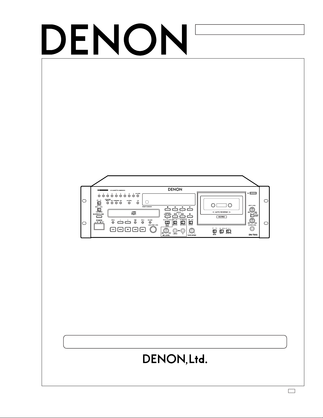
For U.S.A., Canada & Europe model
SERVICE MANUAL
MODEL
CD/CASSETTE COMBI-DECK
(This illustration shows the DN-T645 model.)
DN-T645/625
1 Some illustrations using in this service manual are slightly different from the actual set.
16-11, YUSHIMA 3-CHOME, BUNKYOU-KU, TOKYO 113-0034 JAPAN
Telephone: 03 (3837) 5321
X-0159 NC 0210

DN-T645/625
SAFETY PRECAUTIONS
The following check should be performed for the continued protection of the customer and service technician.
LEAKAGE CURRENT CHECK
Before returning the unit to the customer, make sure you make either (1) a leakage current check or (2) a line to
chassis resistance check. If the leakage current exceeds 0.5 milliamps, or if the resistance from chassis to either
side of the power cord is less than 460 kohms, the unit is defective.
2
2
DISASSEMBLY
(To reassemble, reverse disassembly)
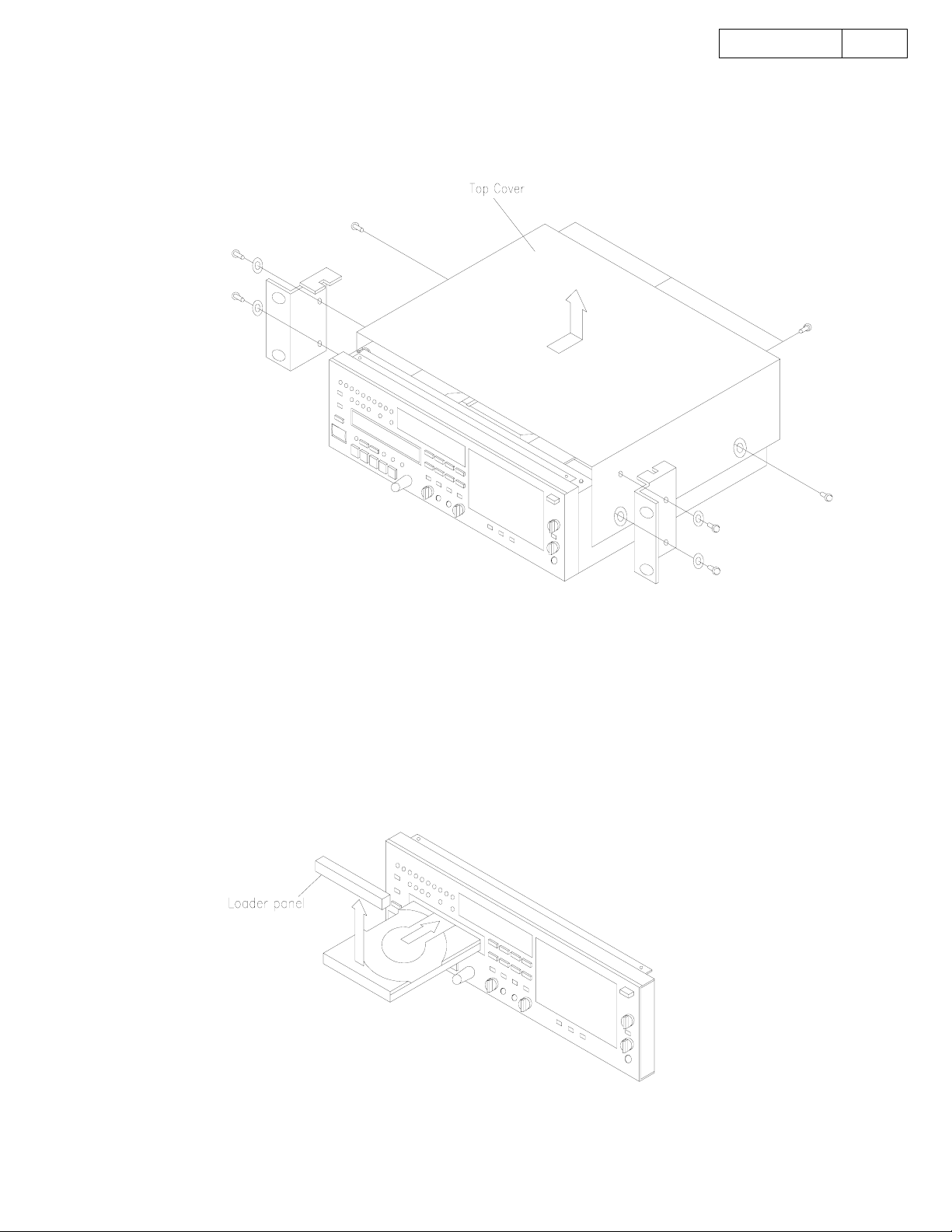
1. TOP COVER
(1) Remove 6 screws on both sides, and 3 screws on the rear panel.
(2) Pull the Top Cover as shown by the arrow direction.
DN-T645/625
3
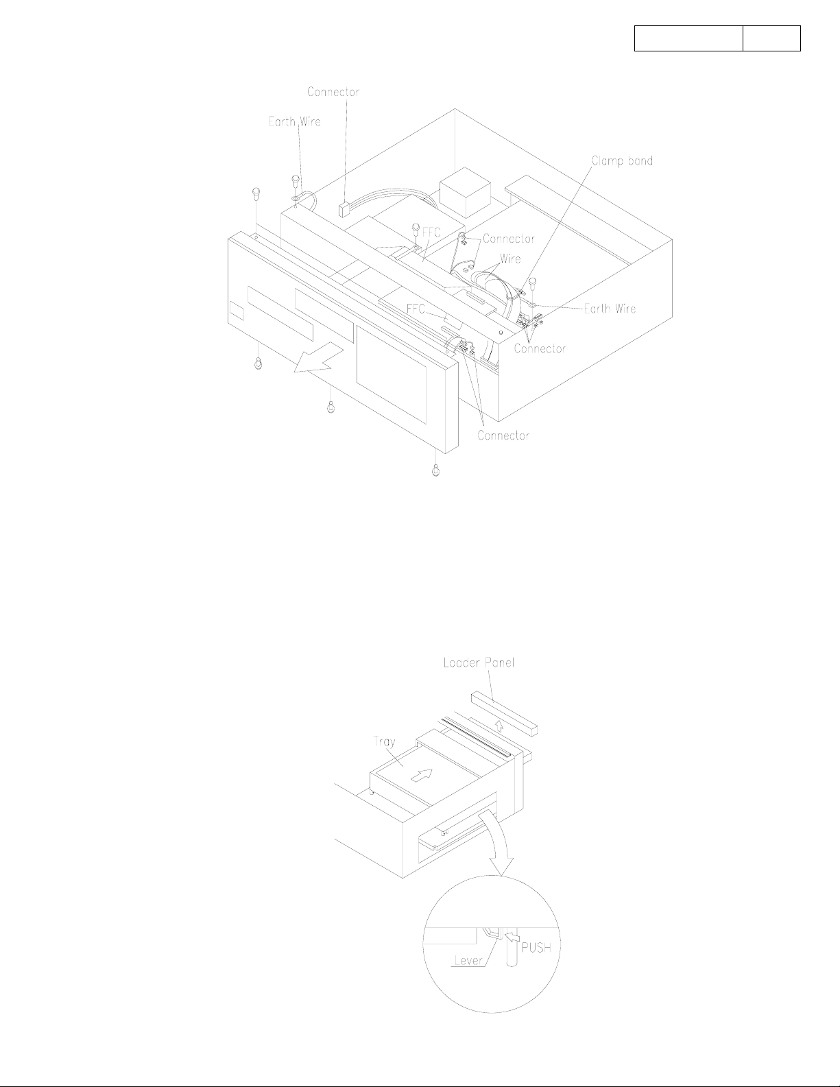
2. FRONT PANEL
(1) Turn the unit power on, and open Tray of the CD Mecha.
(2) Remove the Loader panel, and switch off the power after closing the Tray.
(3) Remove 2 screws at the top, and 3 screws at the bottom.
(4) Remove 2 screws to free Earth Wire.
(5) Remove the screw to free FFC.
(6) Cut the Clamp band.
(7) Disconnect 2 wire and 6 connectors from the Front Panel, then detach the Front Panel to the arrow direction about 50mm.
(8) Disconnect 2 connectors and the FFC from the Front Panel, then detach the Front Panel to the arrow direction.
3
DN-T645/625
4
Method of opening the Tray when the power would not be turned on in trouble.
(1) Please be sure to unplug the cord.
(2) Push the lever indicated in the circled figure below with small bar like a pencil or a ball pointed pen, through the square
opening on the left side of the main chassis.
(3) Push the Tray out to the direction indicated in the figure below.
(4) Detach the Loader Panel by lifting up to the direction indicated bellow.
4
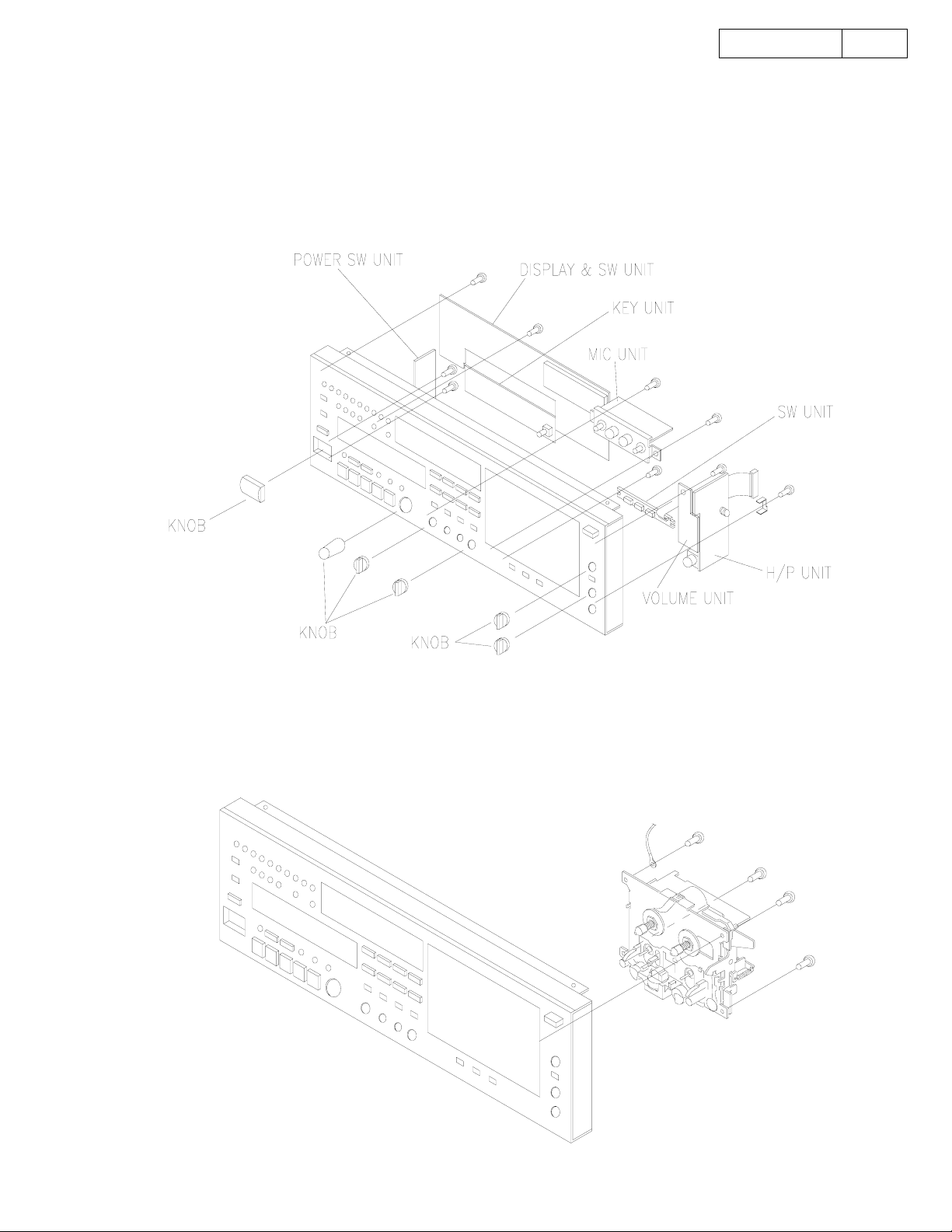
3. DISPLAY & SW UNIT / KEY UNIT / SW UNIT / MIC UNIT /
H/P UNIT / VOLUME UNIT / POWER SW UNIT
(1) Pull out 6 knobs on the front.
(2) Remove 15 screws and 6 screws on the DISPLAY & KEY UNIT.
(3) Remove 2 screw on the MIC UNIT.
(4) Remove the screws on the SW UNIT.
(5) Remove 2 screws on the H/P UNIT & VOLUME UNIT.
(6) remove 2 screws on the POWER SW UNIT.
DN-T645/625
5
4. CASSETTE MECHA
(1) Press Eject button and unlock cassette Door.
(2) Remove 4 screws on the Cassette Mecha.
(3) Detach the Cassette Mecha.
5
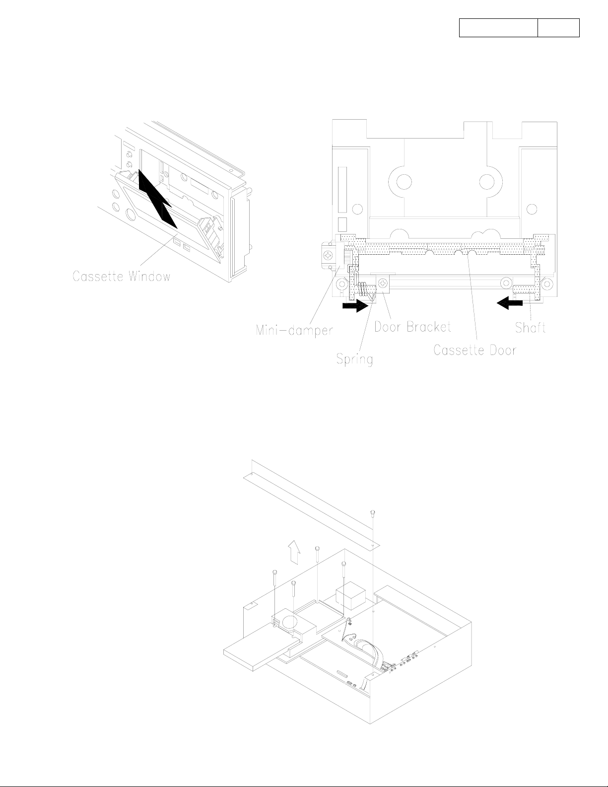
5. CASSETTE DOOR
(1) Take off the Cassette Window on the front.
(2) Remove the screw to detach the Mini-damper.
(3) Remove the screw to detach the Door Bracket.
(4) With pushing the shaft in the arrow directions, no spring side first, detach the Cassette Door.
DN-T645/625
6
6. CD MECHA
(1) Remove 2 screws, then detach the FRONT BRIDGE.
(2) Remove 4 screws.
(3) Pull out the CD Mecha in the arrow direction.
6
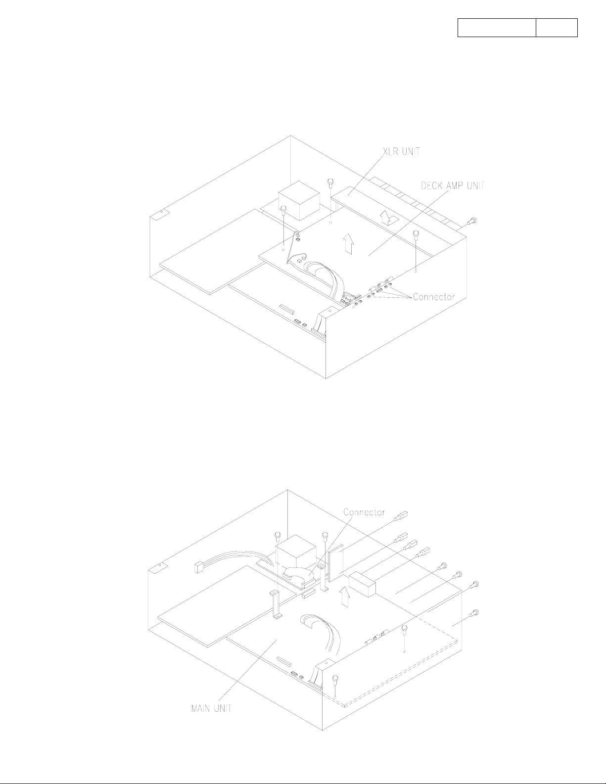
7. XLR UNIT / DECK AMP UNIT
(1) Disconnect the connectors from the DECK AMP UNIT.
(2) Disconnect the FFC and 2 connectors from the MAIN UNIT.
(3) Remove 12 screw, then detach the XLR UNIT to the arrow direction.
(4) Remove 3 screws, then detach the DECK AMP UNIT to the arrow direction.
DN-T645/625
7
8. MAIN UNIT / 25P DSUB UNIT
(1) Disconnect the connectors from the TRANS UNIT.
(2) Remove 8 screws.
(3) Remove 4 hexagon screws, then detach the MAIN UNIT and 25P DSUB UNIT to the arrow direction.
7
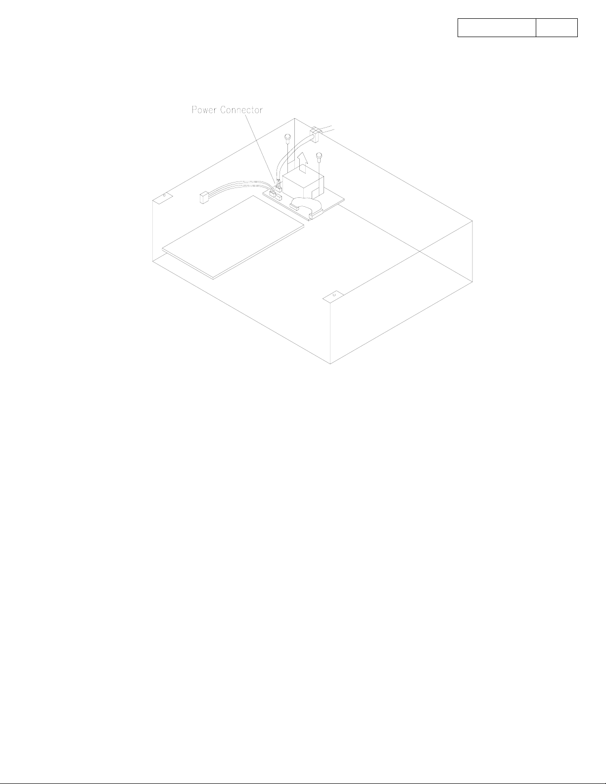
9. TRANS UNIT
(1) Disconnect the power connector.
(2) Remove 4 screws, then detach the TRANS UNIT to the arrow direction.
DN-T645/625
8
8

SERVICE PROGRAM
Required Measuring Implement
z Reference disc (TCD784 or CO-74176)
1. What is Service Program
Service program is a special program intended for confirming servo functions etc.
2. µcom Version Check
z Refer to "Preset Functions and Operations" of the instruction manual.
z You can check the µcom version.
3. Error Data Check
z Switch on the power while pushing the 7 button and 8 button at the same time.
z After actuating the error data check program, press the CD's >> or << button to display the logging error codes
in the occurred order.
XX Err**
Err**: error code (Refer to the "Error Code Table")
z 10 error logs are memorized at maximum. Item 1 is newest data. Item 10 is oldest data. Item 2 is the 9th old data.
z Pressing the 0/CLEAR button enters to data erase mode. ("Err Clear?" is displayed.)
If the 0/CLEAR button is pressed again, the memorized error data are cleared.
z To stop the Error Data check mode, please turn off the POWER switch.
NOTE:
4. Total Running Time
z Switch on the power while pushing the 9 button and 0/CLEAR button at the same time.
Total time span of CD that counted by the hour is displayed.
CD XXXXh
z Press the CD's >> or << button to change the display between CD and DECK.
DEC XXXXh
NOTE:
z Pressing the 0/CLEAR button enters to data erase mode. ("Time Clear?" is displayed.)
If the 0/CLEAR button is pressed again, the memorized time data are cleared.
z To stop the Total Running Time check mode, please turn off the POWER switch.
NOTE:
5. B.E.R. Checks and Automatic Servo Adjustment Call
z Switch on the power while pushing the 5 button and 6 button at the same time.
And Loading a disc by OPEN/CLOSE button.
(1)Block Error Rate
Press the PLAY/PAUSE button. B.E.R. is displayed.
01Tr **m XXXX
You can select the track by the select knob.
(2)Tracking balance and Focus balance data
Press the 2 button. Tracking balance and Focus balance data is displayed.
2 ±XXX±@@@
@@@: Focus balance
(3)Focus gain data
Press the 3 button. Focus gain data is displayed.
3 XXXX
(4)Tracking gain data
Press the 4 button. Tracking gain data is displayed.
4 XXXX
(5)Tracking offset and Focus offset data
Press the 5 button. Tracking offset and Focus offset data is displayed.
5 ±XXX±@@@
@@@: Focus offset
(6)Press the 1 button to select the Block Error Rate data.
(7)To stop the B.E.R. Check and Automatic Servo Adjustment Call mode,
please turn off the POWER switch.
XX: occurred order
When the service is finished, delete the error logs.
Time is counted if powered down first 30 minutes.
When the replacing the associated parts, delete the ranning time.
XXXX: Block Error Rate
XXX: Tracking balance
XXXX: Focus gain
XXXX: Tracking gain
XXX: Tracking offset
9DN-T645/625
No. botton Adjustment Item Adjustment Value indicator
2
3 Focus Gain 0576 ~ 2304
4 Tracking Gain 0392 ~ 1569
5
Tracking Balance -025 ~ +025
Focus Balance -030 ~ +030
Tracking Offset -005 ~ +005
Focus Offset -005 ~ +005
9
6. Test Mode (Heat Run mode)
z Switch on the power while pushing the 3 button and 4 button at the same time.
"
000TroHR0000
(1)Hold the disc by the edges and place it on the disc tray.
(2)Starting with the OPEN/CLOSE button, it repeats open/close of the tray and playback.
***TrxHRXXXX
x : o, c, s, t, r, and p
XXXX: Cycle quantity
All tracks are played back if the track count is less than 20.
Only the first and last tracks are played back if the tracks are more than 21.
When any errors, it stops and indicates error code (Refer to the Error Code Table).
(3)To stop the Test mode, please turn off the POWER switch.
" is displayed. And the tray is opened.
***: Track No.
7. Error Code Table
Error Code CONTENTS
Error 01 Unable to close the loader tray in the regulation time.
Error 02 Unable to open the loader tray in the regulation time.
Error 03 Inner circle switch ON error even if the time is over.
Error 04 Inner circle switch OFF error even if the time is over.
Error 05 The focus offset adjustment result is outside the regulation range.
Error 06 Unable to adjust the focus offset in the regulation time.
Error 07 The tracking offset adjustment result is outside the regulation range.
Error 08 Unable to adjust the tracking offset in the regulation time.
Error 09 The FE peak is outside the regulation range.
Error 0A The FE peak is outside the regulation range.
Error 0B Unable to adjust the focus rough gain in the regulation time.
Error 0C The focus rough gain is outside the regulation range.
Error 0D Unable to actuate focus in the regulation time.
Error 0E Unable to actuate tracking in the regulation time.
Error 0F Unable to adjust the tracking rough gain in the regulation time.
Error 10 The tracking rough gain is outside the regulation range.
Error 11 Unable to adjust the tracking balance in the regulation time.
Error 12 The tracking balance adjustment result is outside the regulation range.
Error 13 Focus servo down during automatic adjustment.
Error 14 Focus servo down during automatic adjustment.
Error 15 Unable to adjust the focus balance in the regulation time.
Error 16 The focus balance adjustment result is outside the regulation range.
Error 17 Track servo down during automatic adjustment.
Error 18 Unable to adjust the focus fine gain in the regulation time.
Error 19 The focus fine gain is outside the regulation range.
Error 1A Unable to adjust the tracking fine gain in the regulation time.
Error 1B The tracking fine gain is outside the regulation range.
Error 1C Unable to adjust automatically in the regulation time.
Error 1D Unable to read the subcode Q in the regulation time.
Error 1E Unable to read the TOC in the regulation time.
Error 1F Focus servo down during search (over the regulation time).
Error 20 Track servo down during search (over the regulation time).
Error 2116 Servo error during search.
Error 2103 Search error (over the regulation time).
Error 22 Discontinuity occurred, during write to the DRAM.
Error 23 The error which cannot be corrected to the read data.
Error 24 Unable to do the level detect.
Error 25 Unable to join data in the regulation time.
Error 26 The error rate when recording on the memory is over the regulation value.
Error 27 The subcode jump more than regulation.
10DN-T645/625
10

µCOM VERSION UPGRADE
System µcom can be upgraded in the following manner.
Version Upgrade Method
1.Record the version upgrade software on a CD-R or CD-RW disc,
only as one file with the format ISO9660 Mode-1.
The file name of the supplied version upgrade software should be used as is and this disc needs
to finalize.
2.Hold the disc by the edges and place it on the disc tray.
3.Press the OPEN/CLOSE button to start the version upgrade.
"
Version Up
xxxx : current version
XXXX : upgrade version
4.Press the PLAY/PAUSE button.
"
Now Writing
XXX : count up from 000 to129
5.When the version upgrade is finished, "
6.Turn off the power once and turn on again.
Press the OPEN/CLOSE button and remove the disc.
NOTE:
"→"
Push Play!
" → "
Writing-XXX
When the power is turned off before "
" "
xxxx->XXXX
" are displayed.
Complete!
" are displayed.
" is indicated.
Complete!
" is displayed,
version is not written correctly.
µcom
11DN-T645/625
11
ADJUSTMENT
ADJUSTING AND CHECKING THE
MECHANISM SECTION
1. Replacing Pinch Roller
Before replacing the pinch roller, clean the tape contact
surface of the pinch roller and the capstan shaft.
Most causes of poor tape transport can be traced to dirty
pinch roller and capstan shaft.
Removing the pinch roller
Remove the clips that press the pinch roller and pull the
pinch roller forward remove it.
After replacing, run a padles C-90 tape to check for tape
curls at the tape guide section of the head.
12DN-T645/625
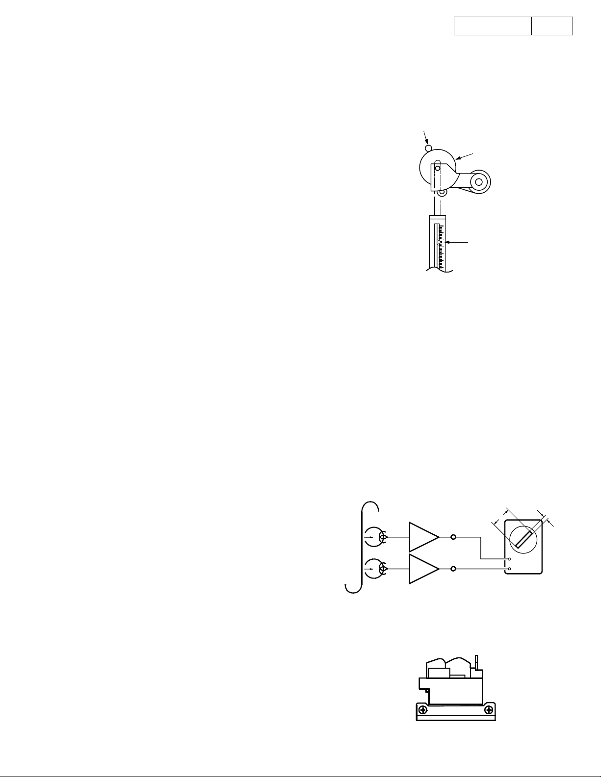
Capstan shaft
Pinch roller
2. Checking the pressure Force of the Pinch
Roller
In the playback mode, hook a spring weight onto the
bracket at the center of the pinch roller. After separating
the pinch roller from the capstan shaft allow the pinch roller
to contact the capstan shaft again. Check to make sure
the spring weight reads between 250 ~ 350g when the
pinch roller starts to rotate.
Replace the pinch roller when it does not conform to the
standard specification values.
3. Replacing the Head Ass'y
(1) Removing the head Ass'y
1. Remove the head base mounting screws.
2. Remove the head base from the lead holder and
the wire connectors.
(2) Head Ass'y Installation
1. Assembly is the reverse of disassembly.
4. Adjusting the R/P HEAD
Azimuth adjustments
Set test tape A-BEX TCC-153 so that the A surface faces
forward, and adjust accordingly.
(1) Playback FWD. Turn the azimuth adjustment nut so
that the Lissajous waveform (A) is at maximum scale
and the Lissajous waveform (B) is at minimum scale.
(2) Playback REV. Turn the azimuth adjustment nut in
the same manner as (1), above.
(3) Make further adjustments to (1) and (2), above.
(4) Apply torsion locks to the adjusted nuts.
Note: Only the azimuth adjustment is necessary; no height
and tilt angle adjustments are required.
A-BEX TCC-153
PB Amp
L
R
LINE OUT
250 ~ 350g
A
B
V
H
12
R/P Head
FWD REV

13DN-T645/625
5. Checking the Take-up Torque
Load the cassette type torque meter
FWD side .........SONY TW2111A
REV side ..........SONY TW2121A
Check to make sure that the average torque meter reading
is within 30 ~ 70g-cm during playback. If it is not within
this range, check the voltage (approx. 4V) of the reel motor.
After the verification, replace the reel motor if there is no
problem with the voltage value.
6. Checking the FF and REW Torques
Load the cassette type torque meter (SONY TW2231).
Check to make sure the torque meter indicates within
90 ~ 180g-cm at the end of FF and REW.
7. Checking the Back Tension Torque During
Record/Playback
Load the cassette type torque meter
FWD side .........SONY TW2111A
REV side ..........SONY TW2121A
Check to make sure the torque meter reads between
2 ~ 6g-cm during playback and that there is no unevenness.
8. Checking the FF and REW Times
Load a C-60 cassette tape (TDK AC-514); check to make
sure the tape is fast forwarded or rewound within 85 ~
115 seconds. If it is not within this range, check sections 5
and 7.
9. Checking the Operation of the Erase
Prevention, Metal and Chrome Switch
Confirm that the sensor arm properly detecting the tape
type detection holes on the cassette housing.
Caution on adjusting
(1) Before adjusting, clean the head surface, capstan and
the pinch roller with a gauze or cotton swab moistened
with alcohol.
(2) Demagnetize the R/P HEAD and the E HEAD with a
head eraser.
(3) Completely demagnetize the adjustment screwdriver.
(4) Unless instructed otherwise, set the various controls
as follows:
INPUT volume ....................... maximum
DOLBY NR button ................. OFF
TAPE SPEED ....................... Center click position
PHONES SELECT ................ TAPE/MIX
INPUT SELECT .................... LINE
1. Tape Transport Check
Load the transport check cassette. In the operational mode,
illuminate the fixing guides of the R/P HEAD with a lamp
and check to make sure the tape edge does not come in
contact with the tape guide section.
The tape transport is the most important element in
determining the performance of a cassette deck.
Avoid moving the various adjustment screws, nuts, etc.,
as much as possible. Refer to the pages on "Adjusting
and Cheking the Mechanism Section" when replacing or
adjusting the R/P HEAD.
2. Adjusting the Azimuth
(1) After completing the tape transport check, load the
test tape (A-BEX TCC-153).
(2) Playback (both FWD side and REV side) the test tape;
adjust the azimuth screw so that section A of the
Lissajous waveform is maximum and section B is
minimum.
ADJUSTING THE ELECTRICAL SECTIONS
Measuring instruments necessary for
adjustments
(1) Audio signal generator
(2) Variable resistance attenuator
(3) Electronic voltmeter
(4) Oscilloscope
(5) Frequency counter
(6) Adjustment screwdriver.
(7) Trap coil adjustment square stick
(8) Test tapes (SONY TY-224)
(A-BEX TCC-130, TCC-153, TCC-262B/162B)
(TDK AC-514)
(9) Transport Check cassette tape (A-BEX TCC-902)
A-BEX TCC-153
FWD REV
PB Amp
L
R
LINE OUT
R/P Head
A
V
H
B
13
3. Checking and Adjusting the Tape Speed
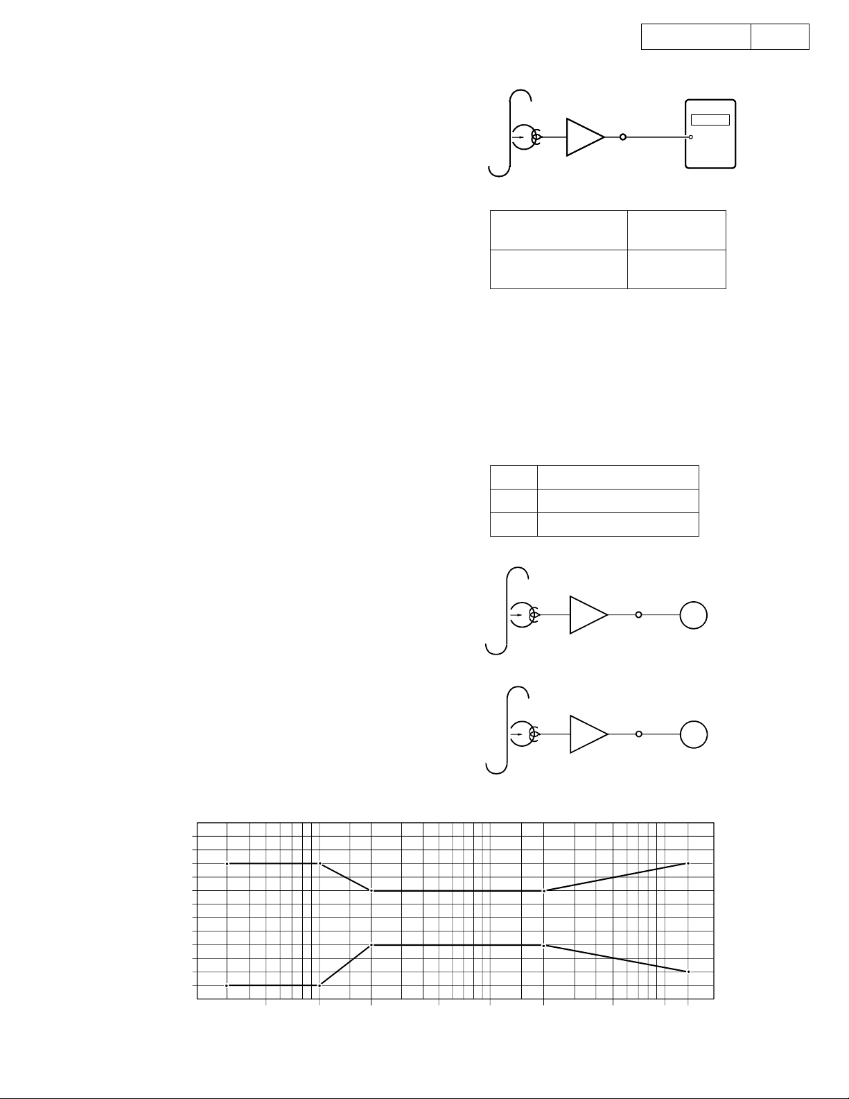
(1) Connect the frequency counter to the LINE OUT
terminal and load test tape (SONY TY-224).
(2) Load cassette tapes and playback test tape.
(3) At about halfway through the tape, where the tape
transport is stable, adjust the VR-502.
14DN-T645/625
F. Counter
PB Amp
LINE OUT
4. Playback System Adjustment
(1) Playback level
Playback a test tape for Dolby standard level (A-BEX
TCC-130). Adjust (Lch) and (Rch) so that the LINE
OUT terminal level is at 0 dB (775 mV).
(2) Verifying playback frequency characteristics
Playback the test tape (A-BEX TCC-262B/162B) and
verify that the frequency characteristics conform to
the specified standard.
Note: Before checking the playback frequency response,
first adjust the azimuth using the 8 kHz signal at the
beginning of the test tape (A-BEX TCC-262B). Also,
after checking the playback frequency, make sure
to readjust the azimuth with the test tape (A-BEX
TCC-153) and then lock the adjustment screw.
SONY TY-224
Adjusting volume
number
VR-502
Playback Level
L/R
Adjusting volume number
L
R
A-BEX TCC-130
F. counter
(Hz)
3005±5
VR-301
VR-302
PB Amp
LINE OUT
V.V
(db)
PB Amp
LINE OUT
A-BEX TCC-262B/162B
V.V
Playback frequency characteristics
+6
+
5
4
+
+3
+2
1
+
0
1
−
−2
3
−
−4
−5
6
−
20
10050
200
500
1 k
2 k
5 k
10 k 12 k
20 k (Hz)
Tape: A-BEX TCC-262B/162B
14
15DN-T645/625
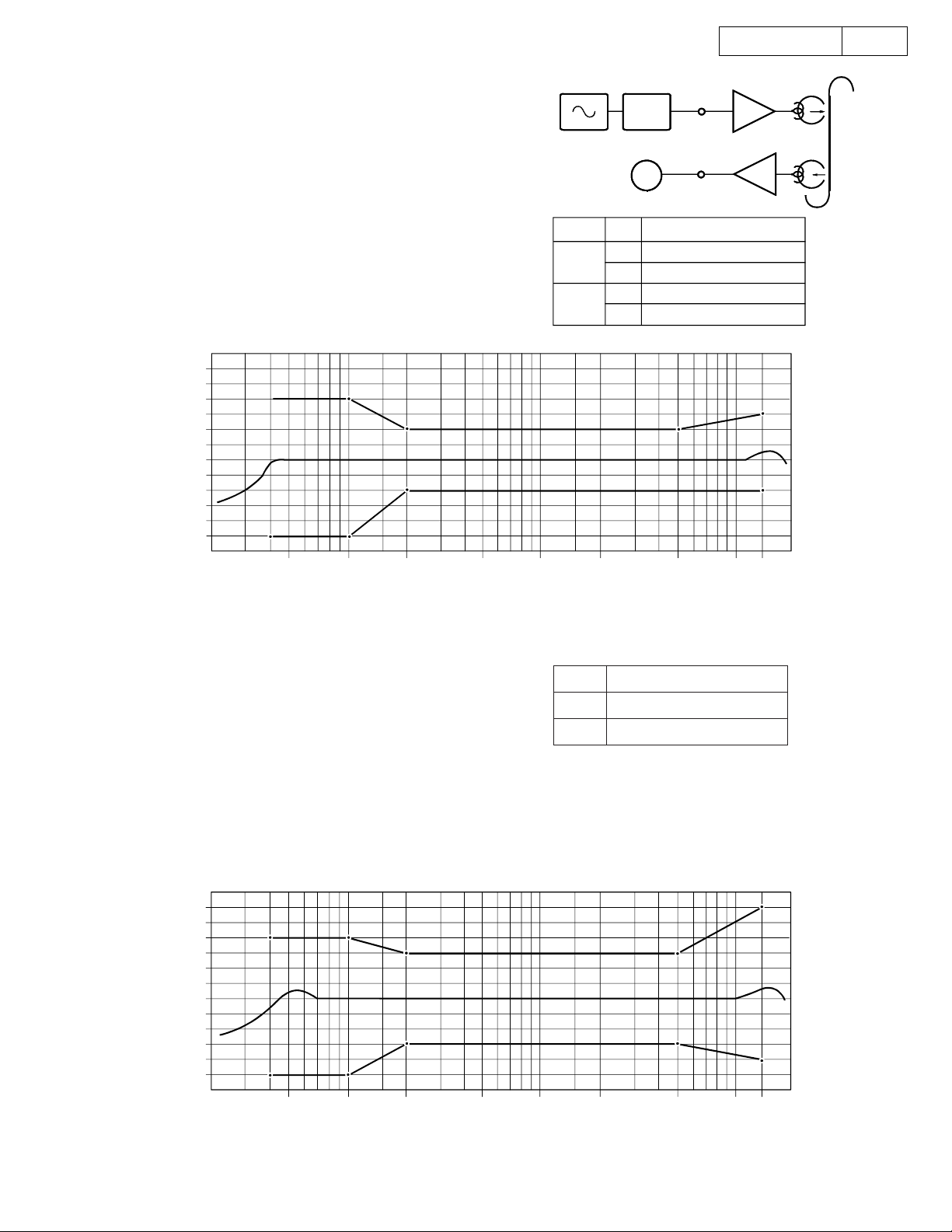
5. Recording System Adjustment
5-1. Adjusting recording/playback comprehensive
frequency characteristics.
(1) Load a test tape TDK AC-514.
Record with a -20 dB 1 kHz input level signal into
the LINE IN terminal and playback.
(2) Make a sample recording using a 12 kHz input
signal and playback this recording. Adjust (left
channel) and (right channel) so that they conform
to the following specified characteristics.
(db)
+6
+5
+
4
+
3
2
+
+1
0
−1
−2
−3
−4
5
−
−
6
20
Record/Playback Overall Frequency Response
10050
200
500
Frequency Responce
L/R
DN-T
645
DN-T
625
1 k
L VR-551
R
L
R
2 k
Tape
Dolby NR
Level
REC Amp
LINE IN
ATT
LINE OUT
V.V
PB Amp
Adjusting volume number
VR-552
VR-582
VR-581
5 k
: AC-514
: Off
: −20 dB From Dolby Level
10 k 12 k
20 k (Hz)
5-2. Recording/Playback Level Adjustment
(1) Load the test tape TDK AC-514. Make a sample
recording with the 1 kHz (-20 dB) signal and play
this section back.
(2) Adjust (Lch) and (Rch) so that the output from
LINE OUT terminal is the same as the output at
recording monitoring time.
5-3. Dolby C recording and playback comprehensive
frequency characteristics verification
(1) Set the Dolby NR switch at "C" position.
(2) Use a test tape TDK AC-514 and record and
playback as in item 5-1 to verity that they satisfy
the characteristics standards.
Dolby C Record/Playback Overall Frequency Response
(db)
6
+
+5
4
+
+3
2
+
+
1
0
−1
−
2
3
−
−4
5
−
−6
20
10050
200
500
R/P Level Adjustment
L/R
Adjusting volume number
L
R
1 k
2 k
Tape
Dolby NR
Level
VR-303
VR-304
5 k
: AC-514
: On C
: −20 dB From Dolby Level
10 k 12 k
20 k (Hz)
15
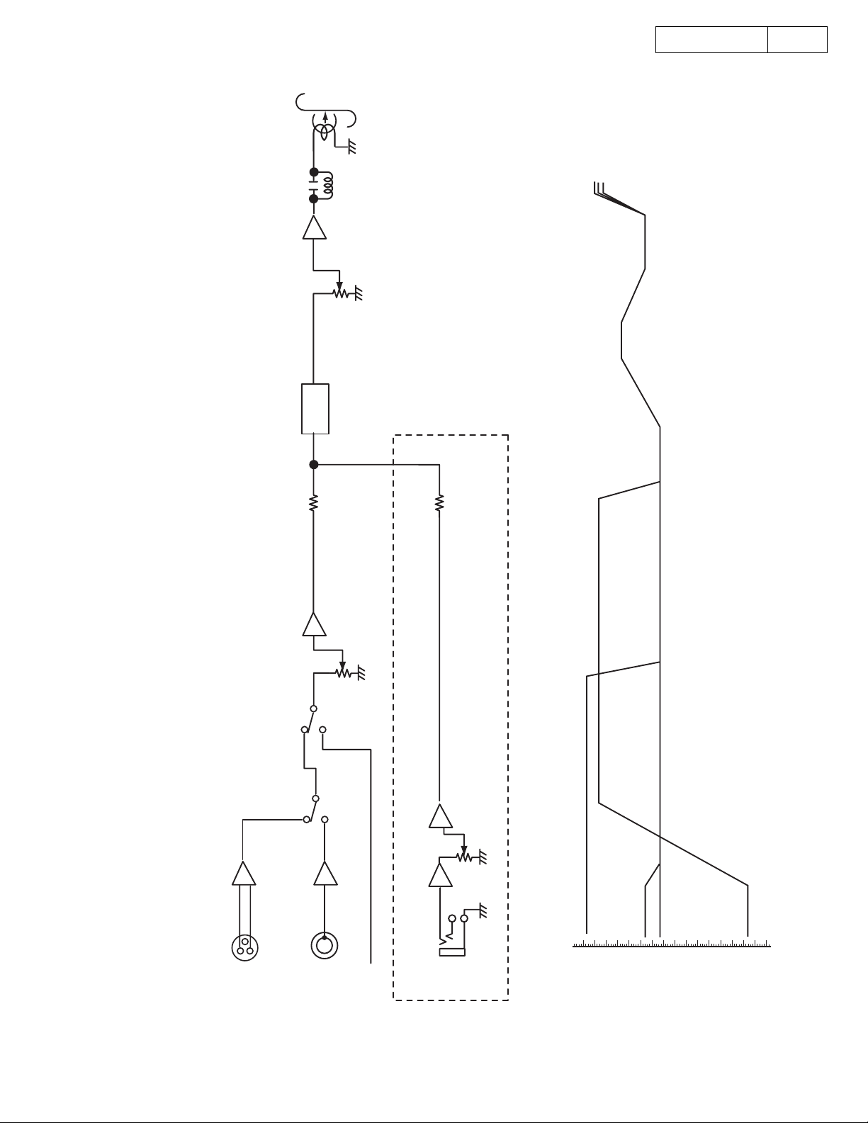
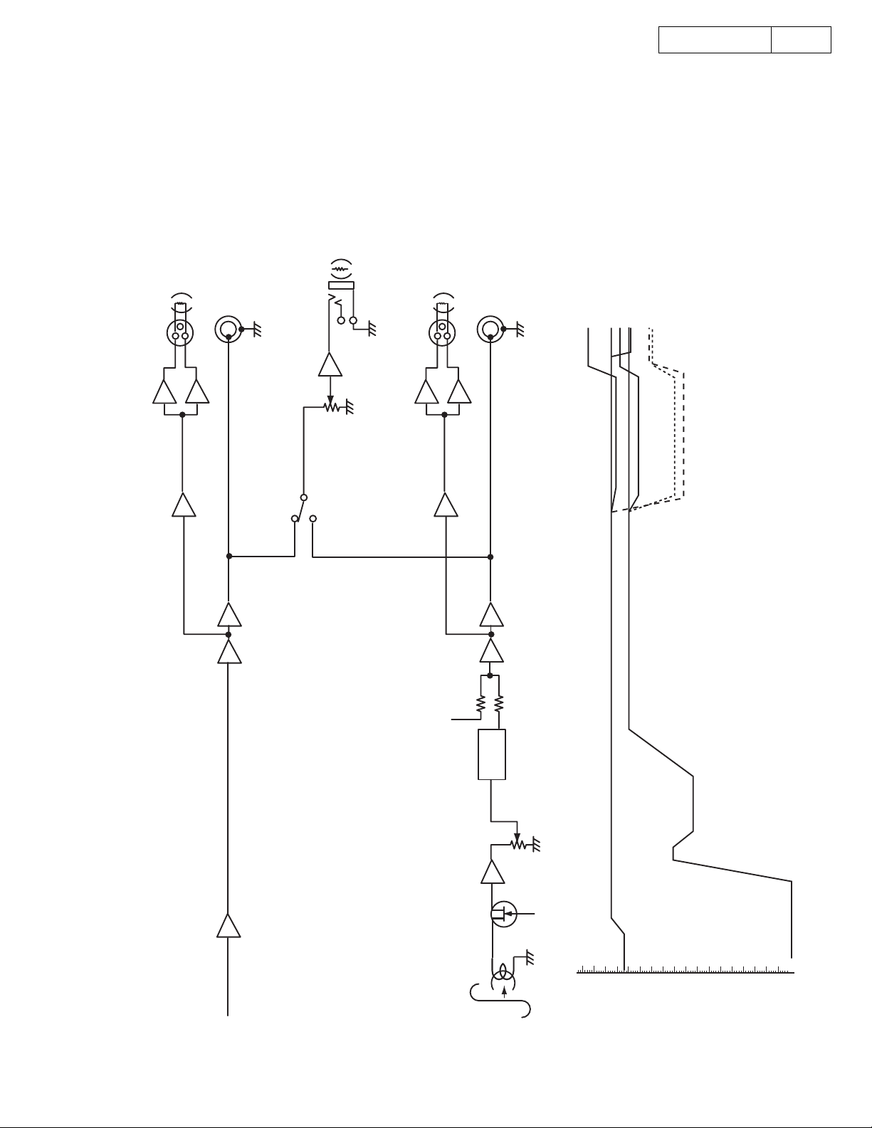
LEVEL DIAGRAMS (1/2)
1(7)
-1dB (NORMAL)
+2.5dB (METAL)
+1dB (CHROME)
DN-T645/625
16
IC304
IC601
IC302
HA12170
16(15)
30(1)
1(7)
VR303(304)
-19dB
+8.2dB
# A : VR621 ADJUST
# A
Not used for Model DN-T625
LEVEL DIAGRAM
1(7)
IC801
ACD 780 (Option)
XLR
RECORDING SYSTEM
INPUT FREQUENCY 400Hz
IC309
RCA
VR621
7(1)
LINE IN
(CD)
IC-651(652) IC-653
16
7
MIC
7(1)
(CD) +8dB
(dBV)
+2.5dB
0dB
RCA -24dB
XLR -17.5dB
-10dB
-20dB
-30dB
-40dB
0dB=0.775V
-50dB
MIC MODE=REC
MIC AGC=OFF
MIC -62dB
-70dB
-60dB
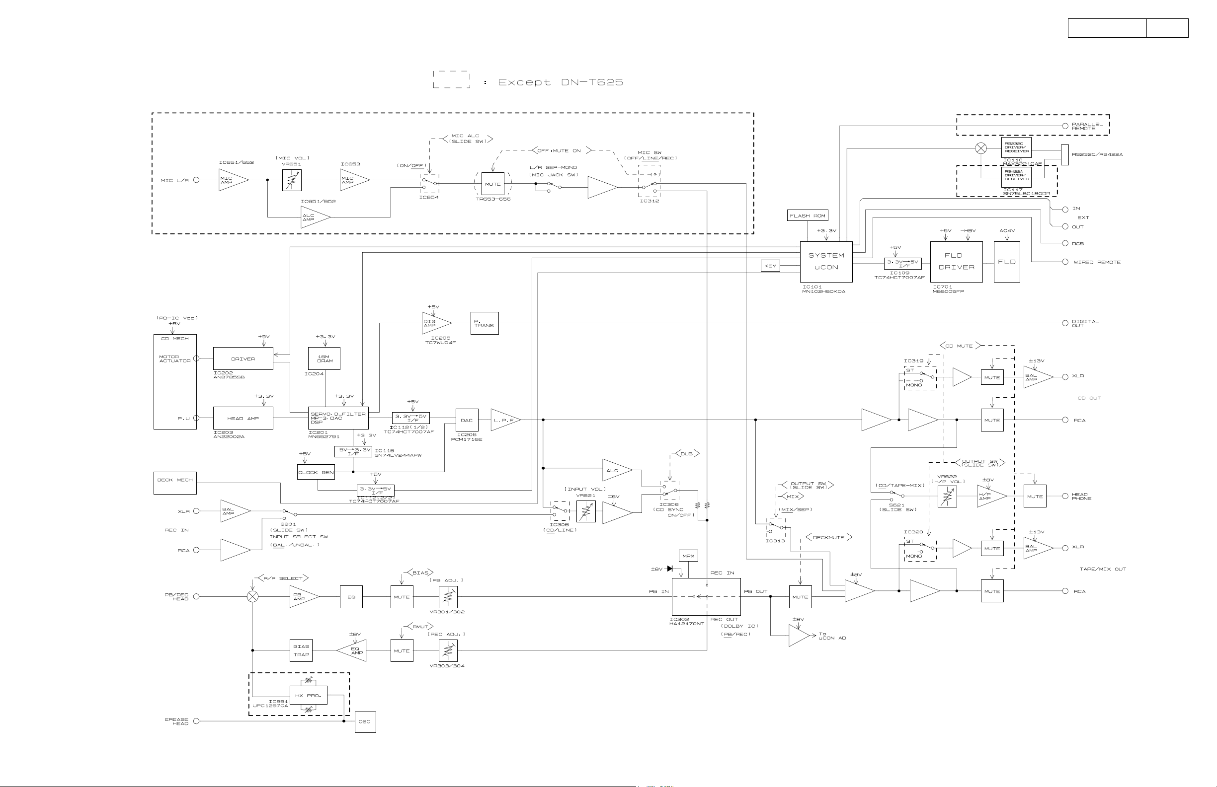
LEVEL DIAGRAMS (2/2)
LOAD
600 ohm
XLR
LINE OUT
RCA
LOAD
33 ohm
IC602
HEADPHONE
1(7)
LOAD
600 ohm
XLR
RCA
LINE OUT
0dB (RCA)(TAPE)
-1dB (HEADPHONE)(CD)
+4dB (XLR)(TAPE)
+18dB (XLR)(CD)
+8dB (RCA)(CD)
DN-T645/625
-9dB (HEADPHONE)(TAPE)
-10dB (XLR)(CD/TAPE:MONORAL RCH)
17
IC804(805)
IC317
1(7)
IC315
IC314
1(7)
1(7)
IC601(603)
IC319
1(7)
IC322
IC321
1(7)
1(7)
IC302
HA12170
28(3)
22(9)
VR301(302)
-28dB
0dB=0.775V
PLAYBACK SYSTEM
IC207
CD
1(7)
IC301
NJM2068
TR301(302)
TAPE
TCC-130 DOLBY B-TYPE
17
7(1)
3(5)
(dBV)
+20dB
+8dB
+10dB
+2dB
0dB
-10dB
-19dB
-20dB
-30dB
-40dB
-50dB
-60dB
-71dB
-70dB
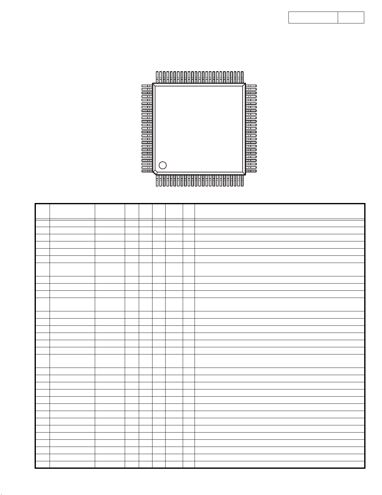
BLOCK DIAGRAM
DN-T645/625
18
18
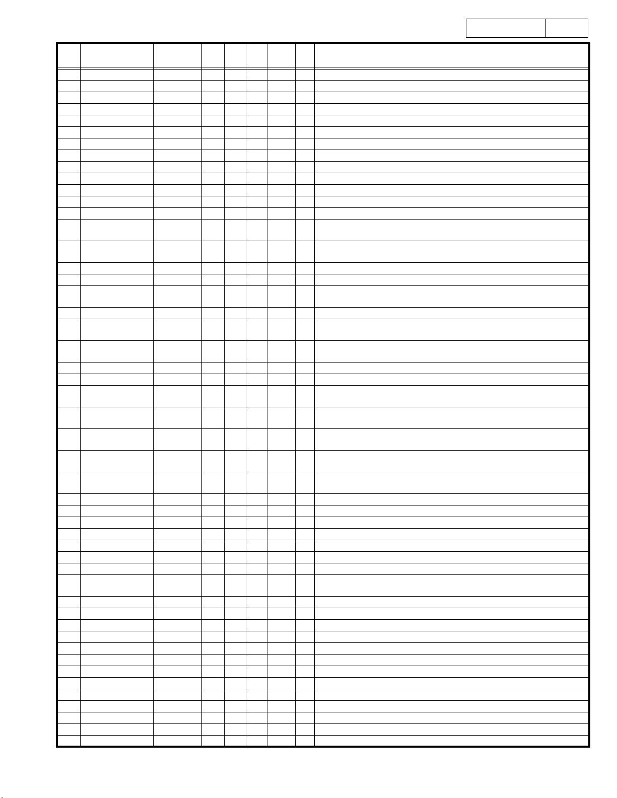
SEMICONDUCTORS
IC’s
MN102H60KDA
(IC101)
DN-T645/625
19
75
76
100
1
51
50
26
25
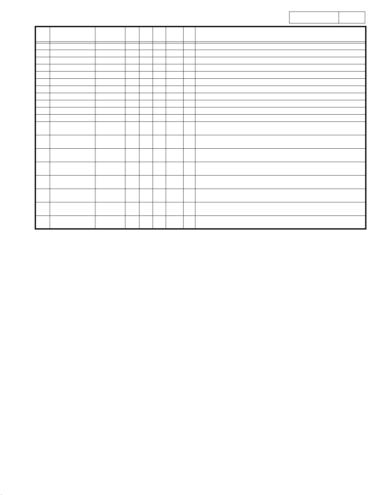
MN102H60KDA Terminal Function
Pin
No.
1 P60, WAIT, SBT2 PCDMUTE O - Pd L L Mute for CD
2 P61, _RE _RD O - - Hi-Z - Read signal
3 P62, _WEL _WEL O - - Hi-Z - Write signal
4 P63, _WE, _WEH PEXTIN I - - Hi-Z - EXT.IN signal
5 _CS0,TM13OA _CS0 O - - Hi-Z - Chip select signal (MASK ROM operation : Input port)
6 _CS1, TM13OB _CS1 O - - Hi-Z - Chip select signal (IN/OUT)
7 _CS2, TM14OA _CS2 O - - Hi-Z - Chip select signal (Normal operation : Input port, MASK ROM operation
8 _CS3, TM14OB _CS3 O - - Hi-Z - Deck (Input/Output)
9 P54, _BREQ PEXTOUT O - - Hi-Z H EXT.OUT signal
10 P55, _BRACK PRMTOUT O - - Hi-Z H Remote output signal
11 P56, ALE, _ALE,
12 P57,_WORD _WORD I - H H H Data bit bus width select 'H': 8bit
13 P20,A00,SBT2 A00 A/O - - Unfix - Address bus
14 P21,A01,SBI2 A01 A/O - - Unfix - Address bus
15 P22,A02,SBO2 A02 A/O - - Unfix - Address bus
16 P23,A03 A03 A/O - - Unfix - Address bus
17 Vdd Vdd - - - - - Power supply (+3.3V)
18 BOSC,BIBT1,
19 Vss Vss - - - - - GND(0V)
20 XI,PB1 PCE O - - Hi-Z L Chip select 'L': MN662791 / 'H': BU2618
21 XO XO - - - - - Not used. OPEN
22 Vdd Vdd - - - - - Power supply (+3.3V)
23 OSCI OSCI I - - - 24 OSCO OSCO O - - - - OSCI output
25 MODE MODE I - L L L Mode select 'L': Processor mode
26 P24,A04,TM15IA A04 A/O - - Unfix - Address bus
27 P25,A05 A05 A/O - - Unfix - Address bus
28 P26,A06 A06 A/O - - Unfix - Address bus
29 P27,A07 A07 A/O - - Unfix - Address bus
30 P30,A08,_KI0 A08 A/O - - Unfix - Address bus
31 P31,A09,_KI1 A09 A/O - - Unfix - Address bus
32 P32,A10,_KI2 A10 A/O - - Unfix - Address bus
Pin Name Symbol I/O Det Ext Res Ini Function
: F.ROM Chip select)
PMON2 I - - Hi-Z - Monitor signal 2
_BSTRE, TM15IA
PIRINH O - - Hi-Z L Infrared remote 'L': Enable / 'H': Inhibit
BIBT2,PB0
19
DN-T645/625
20
Pin
No.
33 P33,A11,_KI3 A11 A/O - - Unfix - Address bus
34 AVDD AVDD - - - - - Analog power supply terminal
35 P34,A12,_KI4 A12 A/O - - Unfix - Address bus
36 P35,A13,_KI5 A13 A/O - - Unfix - Address bus
37 P36,A14,_KI6 A14 A/O - - Unfix - Address bus
38 P37,A15,_KI7 A15 A/O - - Unfix - Address bus
39 P40,A16 A16 A/O - - Unfix - Address bus
40 P41,A17 A17 A/O - - Unfix - Address bus
41 P42,A18 A18 A/O - - Unfix - Address bus
42 P43,A19 A19 A/O - - Unfix - Address bus
43 Vref- Vref- - - - - - Standard analog power supply
44 P44,AN4,A20 PPARA1 I Lv - Unfix - Parallel input 1 (Use A/D converter)
45 P45,AN5,A21 PPARA2 I Lv - Unfix - Parallel input 2 (Use A/D converter)
46 P46,AN6,STOP,
47 P47,AN7,WDOUT,
48 P80,TM14OA PSCL O - - Hi-Z H Not used.
49 P81,TM14OB PDUB O - - Hi-Z H Dubbing signal 'L': Dubbing
50 P82,TM0IO,SBI2,
51 P83,TM4IO,SBI3 RxD I - - Hi-Z - Serial port (9600bps by xxMHz)
52 P84,TM7IO,SBO3,
53 P85,TM9IOA,SBO2,
54 Vref+ Vref+ - - - - - Standard analog power supply
55 P86,TM9IOB,SBI4 PFLCS O - - Hi-Z H To FL driver CS
56 P87,TM9IC,SBO4,
57 P90,TM8IOA,BIBT1,
58 P91,TM10IOA,BIBT2,
59 P92,TM10IOB,
60 P93,TM10IC,
61 Vss Vss - - - - - GND (0V)
62 P94,AN0 PADINL I Lv Pd L - Use A/D converter
63 P95,AN1 PADINR I Lv Pd L - Use A/D converter
64 P96,AN2 PREMO1 I Lv - Hi-Z - Use A/D converter
65 P97,AN3 PREMO2 I Lv - Hi-Z - Use A/D converter
66 Vdd Vdd - - - - - Power supply (+3.3V)
67 P70,SBT0,_RAS PMCLK O - - Hi-Z H DSP interface Clock (clock synchronous formula)
68 P71,SBI0,_CAS,
69 P72,SBO0,_UCAS PMDAT O - - Hi-Z H DSP interface Transmission (clock synchronous formula)
70 P73,SBT1,DUMX PTXTCLK O - - Hi-Z H Use during CD-TEXT data read (clock synchronous formula)
71 P74,SBI1 PTXTD I - - Hi-Z - Use during CD-TEXT data read (clock synchronous formula)
72 P75,SBO1 PMLD O - - Hi-Z H DSP interface latch
73 TEST1 TEST1 I - Pu - - Pull up 33 - 50K
74 TEST2 TEST2 I - Pu - - Pull up 33 - 50K
75 _NMI _NMI I Lv - Hi-Z - Need pull up
76 PA0,_IRQ0 PBLKCK I Ed - Hi-Z - Sub code clock interruption
77 PA1,_IRQ1 PDQSY I Ed - Hi-Z - CD-TEXT DQSY Interruption
78 PA2,_IRQ2 PPLS I Ed - Hi-Z - Count by DOWN EDGE. One rotation by three counts.
79 PA3,_IRQ3 PREMOTE I Ed - Hi-Z - RC-5/Infrared remote signal input
80 PA4,_IRQ4,TM15IB PCHGOFT O - Pu H L Off track signal
81 PA5,ADSEP ADSEP I - H H H 'H': Address data separation mode / 'L': Address data common mode
Pin Name Symbol I/O Det Ext Res Ini Function
PPARA3 I Lv - Hi-Z - Parallel input 3 (Use A/D converter)
A22
PSDA I/O - - Hi-Z - Not used.
A23
PMON1 I - - Hi-Z - Monitor signal 1
SBT3,SCL3
TxD O - - Hi-Z H Serial port (9600bps by xxMHz)
SDA3
PFLCLK O - - Hi-Z H To FL driver SCK
SBT4,SCL4
PFLSD O - - Hi-Z H To FL driver SDATA
SDA4
PBIAS O - Pd L L Bias signal 'H': BIAS ON
_DMAREQ1
PRMUTE O - Pu H H Rec mute change signal 'H': MUTE ON
_DMAACK1
PLRCK I Ed - Hi-Z - LRCK : Use for time code creation during MP3 playback.
_DMAREQ0
PNRST O - Pd L L Round IC reset signal
_DMAACK0
PSTAT I - - Hi-Z - DSP interface Reception (clock synchronous formula)
_LCAS
20
DN-T645/625
21
Pin
No.
82 _RST _RESET I Lv - L - Reset signal 'L': RESET
83 Vdd Vdd - - - - - Power supply (+3.3V)
84 P00,D00,AD00 D00 D/O - - Hi-Z - Data bus
85 P01,D01,AD01 D01 D/O - - Hi-Z - Data bus
86 P02,D02,AD02 D02 D/O - - Hi-Z - Data bus
87 P03,D03,AD03 D03 D/O - - Hi-Z - Data bus
88 P04,D04,AD04 D04 D/O - - Hi-Z - Data bus
89 P05,D05,AD05 D05 D/O - - Hi-Z - Data bus
90 P06,D06,AD06 D06 D/O - - Hi-Z - Data bus
91 P07,D07,AD07 D07 D/O - - Hi-Z - Data bus
92 Vss Vss - - - - - GND(0V)
93 P010,D08,AD08,
94 P011,D09,AD09,T
95 P012,D10,AD10,
96 P013,D11,AD11,T
97 P014,D12,AD12,
98 P015,D13,AD13,
99 P016,D14,AD14,
100 P017,D15,AD15,
Pin Name Symbol I/O Det Ext Res Ini Function
TM8IOB
M8IC
TM11IOA
M11IOB
TM11IC
TM12IOA
TM12IOB
TM12IC
PMIX O - Pd L L Deck line out 'H': Mix out of CD+DECK
PPOFF I - - H - 'L': Power failure detection
PDECKMUTO - Pd L L Deck line mute 'L': MUTE ON
POPEN I - - Hi-Z - OPEN switch
PCLOSE I - - Hi-Z - CLOSE switch
PLOAD O - - Hi-Z H OPEN/CLOSE signal (PWM out put) (During Pnrst='L', out put
PWM(50%))
O- -Hi-ZH
PINSW I - - Hi-Z - Inner circle SW
21
MN6627911AC
(IC201)
61
60
41
40
DN-T645/625
22
80
1
20
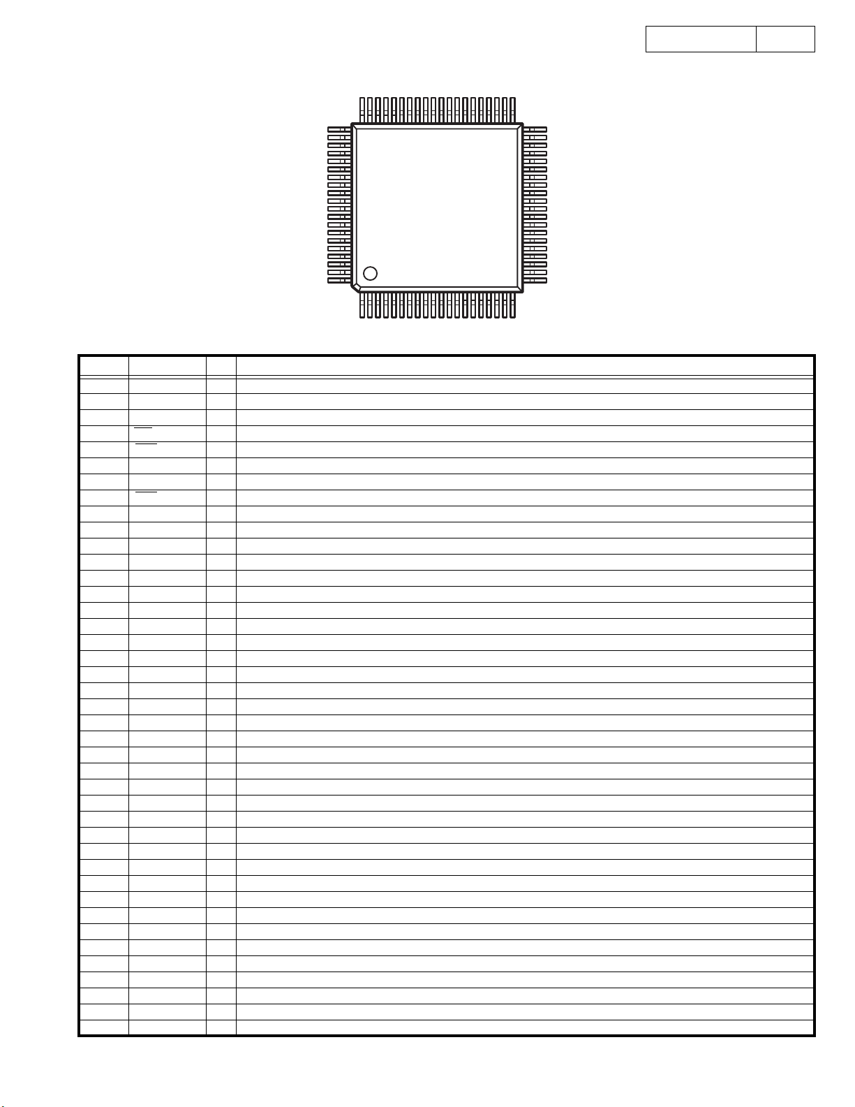
MN6627911AC Terminal Function
Pin No. Pin Name I/O Function
1 DRVDD I Power supply for DRAM interface (Pin No.2 - 18, 80)
2 D0 I/O Data I/O signal 0 for DRAM
3 D1 I/O Data I/O signal 1 for DRAM
4 WE O Write enable signal for DRAM
5 RAS O RAS control signal for DRAM
6 D2 I/O Data I/O signal 2 for DRAM
7 D3 I/O Data I/O signal 3 for DRAM
8 CAS O CAS control signal 0 for DRAM
9 A10 O Address signal 10 for DRAM
10 A8 O Address signal 8 for DRAM
11 A7 O Address signal 7 for DRAM
12 A6 O Address signal 6 for DRAM
13 A5 O Address signal 5 for DRAM
14 A4 O Address signal 4 for DRAM
15 A9 O Address signal 9 for DRAM
16 A0 O Address signal 0 for DRAM
17 A1 O Address signal 1 for DRAM
18 A2 O Address signal 2 for DRAM
19 A3 O Address signal 3 for DRAM
20 DVSS2 I GND for digital
21 DVDD2 I Power supply for digital
22 SPOUT O Spindle motor drive signal
23 TRVP O Traverse drive signal
24 TRVM O Not used
25 TRP O Tracking drive
26 GCNTL O Gain control signal for CD-RW
27 FOP O Focus drive
28 CHGICO O EQ select signal
29 IOVDD1 I Power supply for IO
30 TBAL O Tracking balance adjust
31 FBAL O Focus balance adjust
32 FE I Focus error signal (Analog input)
33 TE I Tracking error signal (Analog input)
34 RFENV I RF envelope signal (Analog input)
35 OFT I Off track signal H : OFF TRACK
36 NRFDET I RF detect signal H : DETECT
37 BDO I Drop out signal H : DROP OUT
38 LDON O Laser ON signal H : ON
39 ARF I RF signal
40 IREF I Standard current input terminal
41 ADPVCC I Voltage for power supply monitor
21
22
Pin No. Pin Name I/O Function
42 DSLF O Loop filter for DSL
43 RFSW I Loop filter for DSL
44 PLLF O Loop filter for PLL
45 PLLFO O Loop filter for PLL
46 AVDD2 I Power supply for analog (DSL, PLL, AD)
47 AVSS2 I GND for analog (DSL, PLL, AD)
48 OUTL O Not used
49 AVSS1 I GND for analog (Audio output)
50 OUTR O Not used
51 AVDD1 I Power supply for analog (Audio output)
52 DVSS3 I GND for digital
53 DVDD3 I Power supply for digital
54 TMOD2 I Test terminal L : Normal
55 MON2 O Serial monitor signal 2
56 BCLK O Bit clock for serial data
57 SRDATA O Serial data signal
58 LRCK O L, R discernment signal
59 IOVDD2 I Power supply for IO
60 TX O Digital audio interface signal
61 MCLK I ucon command clock signal
62 MDATA I ucon command data signal
63 MLD I ucon command load signal L : LOAD
64 BLKCK O Sub code block clock signal (f=75Hz : Normal speed playback)
65 PWMSEL I PWM output mode select L : Direct H : 3 values
66 SMCK O Not used
67 SBCK I Not used
68 STAT O Status signal
69 NRST I Reset L : RESET
70 SPPOL O Not used
71 PMCK O Not used
72 DQSY O Pack signal for CD TEXT data
73 TXTD O CD TEXT data signal
74 TXTCK O Ext. clock signal input for CD TEXT resister
75 NTEST I Test terminal H : Normal
76 X2 O Not used
77 X1 I 16.9344MHz input terminal
78 DVSS1 I GND for digital
79 DVDD1 I Power supply for digital
80 MON1 O Serial monitor signal
DN-T645/625
23
23
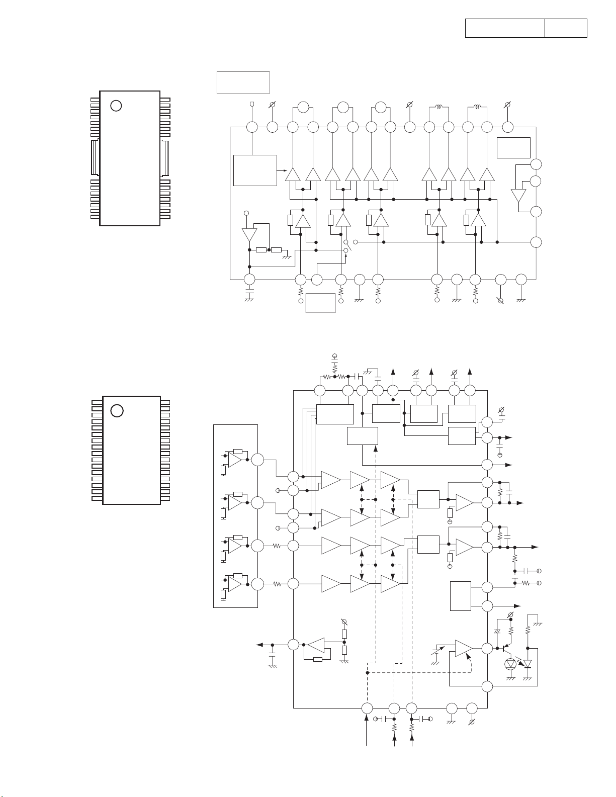
AN8785SB
(IC202)
DN-T645/625
24
1
7
8
14 15
AN22002A
(IC203)
L: All mute
Hiz: ch2,4 ON
H: Active
28
22
21
Standby
16
Standby
Band-gap
Vcc/Vref
Reser Circuit
1.25V
+
-
7
IN2+
0.1µ
(2.5V)
PVcc2
10
[ Loading ]
D2+
D2-
M
12 11
-
+
-
+
9
ch.4 SW
H:2.5V
L or
IN2-
HIZ
-
+
8
:Vref
[ Traverse ]
D4-
18
-+-
21
IN4
[ Others ]
D4+
[ Spindle ]
D3-
D3+
PVcc3
[ Focus ]
D1-
D1+
[ Tracking ]
D5-
D5+
PVcc1
MM
17
14
13
-+-
+
-
+
switch
15
PGnd2
20
IN3
CAGC
+
-
+
ARF
19
CBD0
1
28
-+-+-
-
+
23 27
IN1
PGnd1
C0FTR
BD0
26
+
0FTR
IN5
25
24
Protection
Circuit
4
IN-
-
+
-
+
22
2
SVcc
+
-
SGnd-Fin
5
IN+
3
OUT
6
Vref
RFN
1
16
32
A
+
C
-
+
A
B
+
17
D
-
+
F
-
+
E
-
+
32
C
31
B
30
D
29
27
E
F
28
VREF
17
5
4
RFOUT
RF_EQ
NRFDET
AMP GCA BCA
AMP GCA BCA
GCA
AMP
AMP
GCA
+
-
8
6
7
RFIN
AGC BD0 0FTR
BCA
BCA
12
SUB
SUB
13
3TENV
-
+
-
+
14
9
CEA
10
3TOUT
15
NRFDET
FEN
22
23
FEOUT
TEN
21
20
TEOUT
TEBPF
11
19
VDET
-
+
LD
VDET
18
2
24
PD
1
TBAL
GCTL
24
26
FBAL
25
3
16
VCCGND
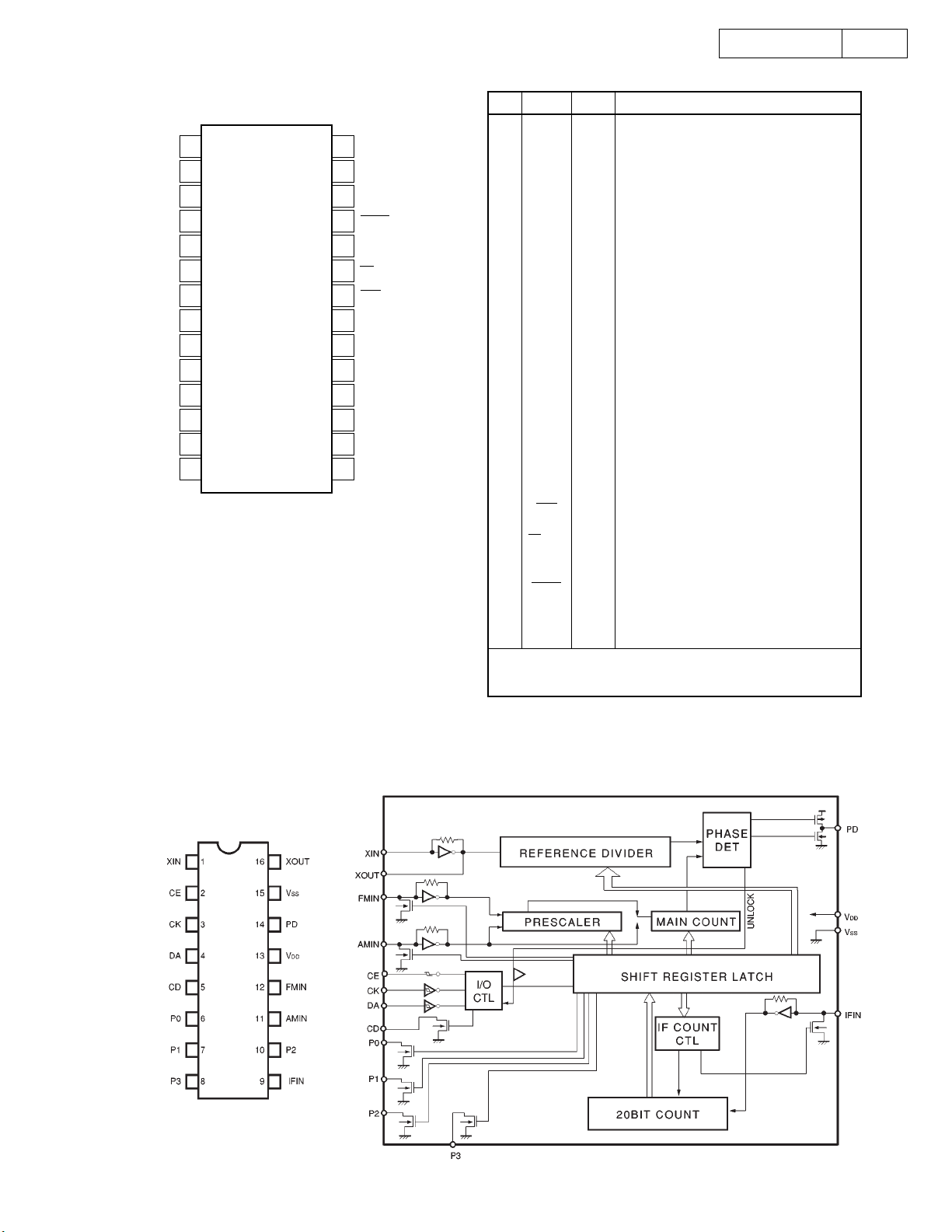
PCM 1716E (IC206)
1
LRCIN
2
DIN
3
BCKIN
4
CLKO
5
XTI
6
XTO
7
DGND
8
V
DD
9
VCC2R
EXTR
NC
V
OUT
AGND1
10
11
12
13
R
14
AGND2R
28
27
26
25
24
23
22
21
20
19
18
17
16
15
ML/IIS
MC/DM1
MD/DM0
MUTE
MODE
CS/IWO
RST
ZERO
V
2L
CC
AGND2L
EXTL
NC
V
L
OUT
V
1
CC
DN-T645/625
PIN NAME I/O DESCRIPTION
1 LRCIN IN Left and Right Clock Input. This clock is equal to
the sampling rate - f
2 DIN IN Serial Audio Data Input
3 BCKIN IN Bit Clock Input for Serial Audio Data.
4 CLKO OUT Buffered Output of Oscillator. Equivalent to
System Clock.
5 XTI IN Oscillator Input (External Clock Input)
6 XTO OUT Oscillator Output
7 DGND
8V
9V
CC
10 AGND2R
-
Digital Ground
-
DD
2R
Digital Power +5V
-
Analog Power +5V
-
Analog Ground
11 EXTR OUT Rch, Common Pin of Analog Output Amp
-
12 NC
13 V
OUT
14 AGND1
15 V
16 V
CC
OUT
1
17 NC
R OUT Rch, Analog Voltage Output of Audio Signal
L OUT Lch, Analog Voltage Output of Audio Signal
No Connection
-
Analog Ground
-
Analog Power +5V
-
No Connection
18 EXTL OUT Lch, Common Pin of Analog Output Amp
-
19 AGND2L
20 V
2L
CC
Analog Ground
-
Analog Power +5V
21 ZERO OUT Zero Data Flag
22 RST IN Reset. When this pin is low, the DF and
modulators are held in reset.
23 CS/IWO IN Chip Select/Input Format Selection. When this
pin is low, the Mode Control is effective.
24 MODE IN
Mode Control Select. (H: Software, L: Hardware)
25 MUTE IN Mute Control
26 MD/DM0 IN Mode Control, DATA/De-emphasis Selection 1
27 MC/DM1 IN Mode Control, BCK/De-emphasis Selection 2
28 ML/I2S IN Mode Control, WDCK/Input Format Selection
NOTES: (1) Pins 1, 2, 3; Schmitt Trigger input. (2) Pins 22, 24, 25, 26, 27,
28; Schmitt Trigger input with pull-up resister. (3) Pin 23; Schmitt Trigger
input with pull-down resister.
(1)
.
S
(1)
(1)
(2)
(3)
25
(2)
(2)
(2)
(2)
BU2618FV (IC113)
25
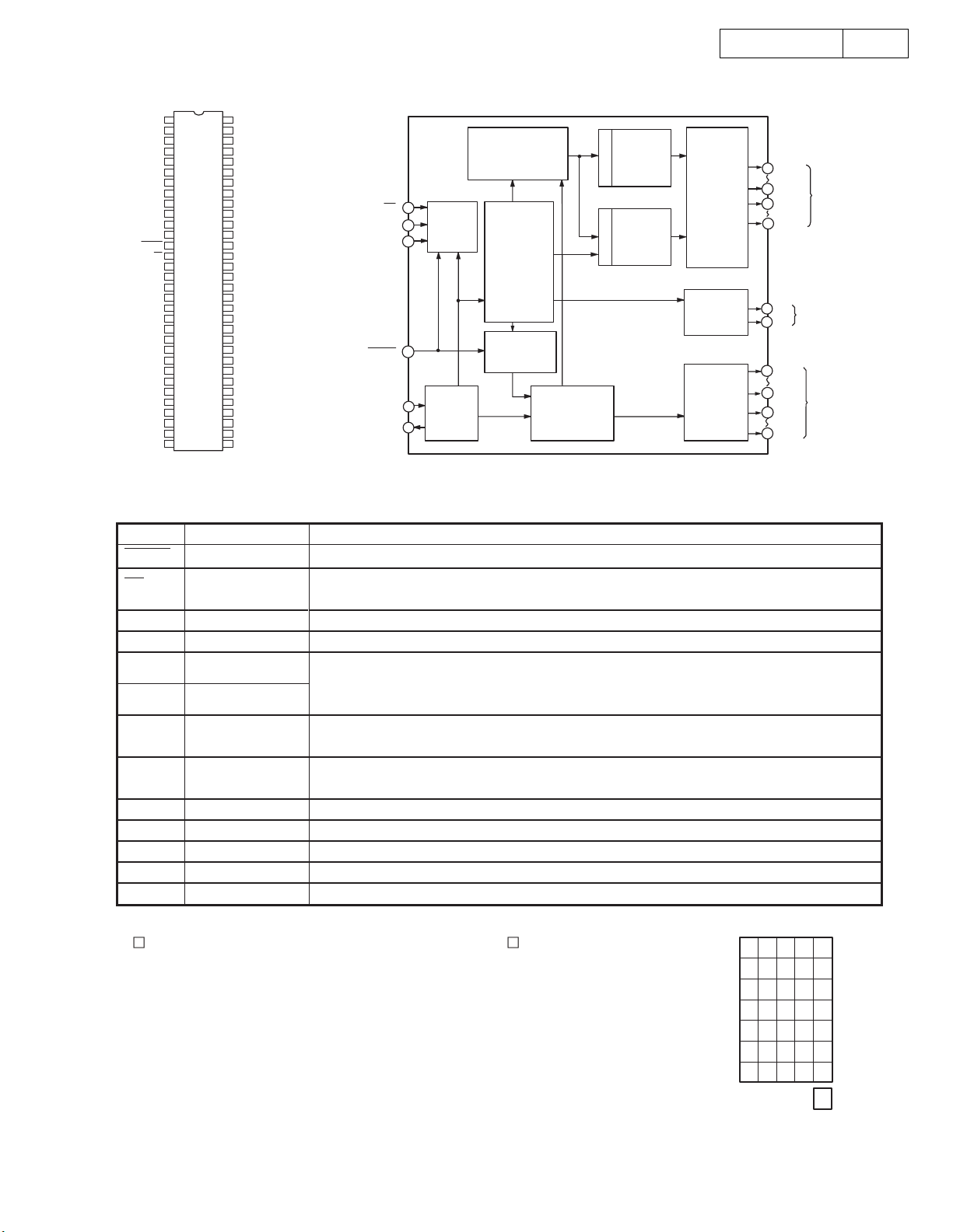
M66005FP (IC701)
D I G
1 1
1
2
D I G
1 0
3
D I G
0 9
D I G
0 8
4
D I G
0 7
5
D I G
0 6
6
D I G
0 5
7
D I G
0 4
8
9
D I G
0 3
D I G
0 2
1 0
D I G
0 1
1 1
D I G
0 0
1 2
1 3
R E S E T
C S
1 4
1 5
S C K
S D A T A
1 6
P I
1 7
P O
1 8
1 9
V c c 1
2 0
X
o u t
2 1
X
i n
2 2
V s s
S E G
2 3
3 5
2 4
S E G
3 4
S E G
3 3
2 5
S E G
3 2
2 6
S E G
3 1
2 7
2 8
S E G
3 0
S E G
2 9
2 9
S E G
2 8
3 0
S E G
2 7
3 1
V p S E G
3 2
D I G
6 4
6 3
D I G
6 2
D I G
D I G
6 1
6 0
V c c 2
5 9
S E G
S E G
5 8
S E G
5 7
5 6
S E G
5 5
S E G
5 4
S E G
5 3
S E G
5 2
S E G
5 1
S E G
5 0
S E G
4 9
S E G
4 8
S E G
4 7
S E G
4 6
S E G
4 5
S E G
S E G
4 4
4 3
S E G
4 2
S E G
4 1
S E G
S E G
4 0
3 9
S E G
3 8
S E G
S E G
3 7
S E G
3 6
3 5
S E G
3 4
S E G
3 3
1 2
1 3
1 4
1 5
0 0
0 1
0 2
0 3
0 4
0 5
0 6
0 7
0 8
0 9
1 0
1 1
1 2
1 3
1 4
1 5
1 6
1 7
1 8
1 9
2 0
2 1
2 2
2 3
2 4
2 5
2 6
C h i p S e l e c t I n p u t
S h i f t C l o c k I n p u t
S e r i a l D a t a I n p u t
R e s e t I n p u t
C l o c k I n p u t
C l o c k O u t p u t
S C K
S D A T A
R E S E T
X O U T
DN-T645/625
D i s p l a y C o d e R e g i s t e r
( 8 - b i t x 1 6 )
c o d e
1 4
C S
S e r i a l
1 5
R e c e p t i o n
C i r c u i t
1 6
1 3
C l o c k
2 1
X I N
2 0
G e n e r a t i o n
C i r c u i t
w r i t e
C o d e /
C o m m a n d
C o n t r o l C i r c u i t
D i s p l a y C o n t r o l
R e g i s t e r
R A M
w r i t e
c o d e s e l e c t
D i s p l a y C o n t r o l l e r
C G R O M
( 3 5 - b i t x 1 6 0 )
D e c o d e rD e c o d e r
C G R O M
( 3 5 - b i t x 1 6 )
S e g m e n t
O u t p u t
C i r c u i t
O u t p u t P o r t
( 2 - b i t )
D i g i t O u t p u t
C i r c u i t
S E G
0 0
5 9
2 6
S E G
3 3
3 1
2 3
1 8
1 7
1 2
1
6 4
6 1
S E G
S E G
P 0
P 1
D I G
D I G
D I G
D I G
2 7
3 5
O u t p u t P o r t
0 0
1 1
D i g i t O u t p u t
1 2
1 5
S e g m e n t
O u t p u t
26
M66005FP Terminal Function
Symbol Name Function
RESET Reset Input
CS Chip Select Input
SCK Shift Clock Input
SDATA Serial Data Input
X
IN
OUT
X
DIG 00~
DIG 15
SEG 00~
SEG 35
Clock Input
Clock Output
Digit Output
Segment Output
P0, P1
V
CC1
V
CC2
Vss
Vp
(Forwarding connection of segment output terminal.)
in the right figure indicates 1 dot of segment, the figure in shows the segment output
terminal number (00~35) to be connected.
Initialzes internal state of M66005.
Able to communicate with MCU in "L" mode.
Command from MCU will be disregareded in "H" mode.
Shifts input data at rise from "L" to "H".
Inputs character code or command data needed to display from MSB.
Sets oscillation frquency by connecting external resistor and capacitor (maximum
oscillation frequency fosc (max)=1MHz). Also feasible to apply external clock. In this case,
inject external clock to Xin terminal and open Xout terminal.
Connect to digit terminal of VFD. DIG00~DIG15 correspond to the 1st figure to 16th figure
respectively.
Connect to segment terminal of VFD. For corresponding SEG00~SEG35 to segment
terminal of VFD, refer to the figure right.
Output port (static operation).
Positive power supply terminal for internal logic.
Positive power supply terminal for high tension output port.
GND terminal.
Negative power supply terminal for VFD drive.
00 01 02 03 04
05 06 07 08 09
10 11 12 13 14
15 16 17 18 19
20 21 22 23 24
25 26 27 28 29
30 31 32 33 34
26
35
 Loading...