

Page 1
For U.S.A., Canada, Europe, U.K.,
Asia, China, Taiwan R.O.C., Korea
& Japan model
2
Ver. 2
SERVICE MANUAL
MODEL DN-S3500
TABLE TOP SINGLE CD PLAYER
注 意
サービスをおこなう前に、このサービスマニュアルを
必ずお読みください。本機は、火災、感電、けがなど
に対する安全性を確保するために、さまざまな配慮を
おこなっており、また法的には「電気用品安全法」に
もとづき、所定の許可を得て製造されております。
従ってサービスをおこなう際は、これらの安全性が維
持されるよう、このサービスマニュアルに記載されて
いる注意事項を必ずお守りください。
Please refer to the
MODIFICATION NOTICE.
●
For purposes of improvement, specifications and
design are subject to change without notice.
●
Please use this service manual with referring to the
operating instructions without fail.
●
Some illustrations using in this service manual are
slightly different from the actual set.
Denon Brand Company, D&M Holdings Inc.
●
●
●
●
TOKYO, JAPAN
本機の仕様は性能改良のため、予告なく変更すること
があります。
補修用性能部品の保有期間は、製造打切後8年です。
修理の際は、必ず取扱説明書を参照の上、作業を行っ
てください。
本文中に使用しているイラストは、説明の都合上現物
と多少異なる場合があります。
X0252V.02 DE/CDM 0511
Page 2
SAFETY PRECAUTIONS
The following check should be performed for the continued protection of the customer and service technician.
LEAKAGE CURRENT CHECK
Before returning the unit to the customer, make sure you make either (1) a leakage current check or (2) a line to chassis
resistance check. If the leakage current exceeds 0.5 milliamps, or if the resistance from chassis to either side of the power
cord is less than 460 kohms, the unit is defective.
LASER RADIATION
Do not stare into beam or view directly with optical instruments, class 3A laser product.
DN-S3500
CAUTION
Please heed the points listed below during servicing and inspection.
◎ Heed the cautions!
Spots requiring particular attention when servicing, such as
the cabinet, parts, chassis, etc., have cautions indicated on
labels or seals. Be sure to heed these cautions and the cautions indicated in the handling instructions.
◎ Caution concerning electric shock!
(1) An AC voltage is impressed on this set, so touching inter-
nal metal parts when the set is energized could cause
electric shock. Take care to avoid electric shock, by for example using an isolating transformer and gloves when
servicing while the set is energized, unplugging the power
cord when replacing parts, etc.
(2)There are high voltage parts inside. Handle with extra care
when the set is energized.
◎
Caution concerning disassembly and assembly!
Though great care is taken when manufacturing parts from
sheet metal, there may in some rare cases be burrs on the
edges of parts which could cause injury if fingers are moved
across them. Use gloves to protect your hands.
◎ Only use designated parts!
The set's parts have specific safety properties (fire resistance, voltage resistance, etc.). For replacement parts, be
sure to use parts which have the same properties. In particular, for the important safety parts that are marked ! on wiring
diagrams and parts lists, be sure to use the designated parts.
◎ Be sure to mount parts and arrange the
wires as they were originally!
For safety reasons, some parts use tape, tubes or other insulating materials, and some parts are mounted away from the
surface of printed circuit boards. Care is also taken with the
positions of the wires inside and clamps are used to keep
wires away from heating and high voltage parts, so be sure to
set everything back as it was originally.
◎ Inspect for safety after servicing!
Check that all screws, parts and wires removed or disconnected for servicing have been put back in their original positions, inspect that no parts around the area that has been
serviced have been negatively affected, conduct an insulation
check on the external metal connectors and between the
blades of the power plug, and otherwise check that safety is
ensured.
(Insulation check procedure)
Unplug the power cord from the power outlet, disconnect the
antenna, plugs, etc., and turn the power switch on. Using a
500V insulation resistance tester, check that the insulation resistance between the terminals of the power plug and the externally exposed metal parts (antenna terminal, headphones
terminal, microphone terminal, input terminal, etc.) is 1MΩ or
greater. If it is less, the set must be inspected and repaired.
CAUTION
Many of the electric and structural parts used in the set have
special safety properties. In most cases these properties are
difficult to distinguish by sight, and using replacement parts
with higher ratings (rated power and withstand voltage) does
not necessarily guarantee that safety performance will be preserved. Parts with safety properties are indicated as shown
below on the wiring diagrams and parts lists is this service
manual. Be sure to replace them with parts with the designated part number.
(1) Schematic diagrams ... Indicated by the ! mark.
(2) Parts lists ... Indicated by the ! mark.
Concerning important safety parts
Using parts other than the designated parts
could result in electric shock, fires or other
dangerous situations.
注 意
サービス、点検時にはつぎのことにご注意願います。
◎注意事項をお守りください!
サービスのとき特に注意を必要とする個所についてはキャ
ビネット、部品、シャーシなどにラベルや捺印で注意事項を
表示しています。これらの注意書きおよび取扱説明書などの
注意事項を必ずお守りください。
◎感電に注意!
(1) このセットは、交流電圧が印加されていますので通電時
に内部金属部に触れると感電することがあります。従っ
て通電サービス時には、絶縁トランスの使用や手袋の着
用、部品交換には、電源プラグを抜くなどして感電にご
注意ください。
(2) 内部には高電圧の部分がありますので、通電時の取扱に
は十分ご注意ください。
◎分解、組み立て作業時のご注意!
板金部品の端面の『バリ』は、部品製造時に充分管理をして
おりますが、板金端面は鋭利となっている箇所が有りますの
で、部品端面に触れたまま指を動かすとまれに怪我をする場
合がありますので十分注意して作業して下さい。手の保護の
ために手袋を着用してください。
◎指定部品の使用!
セットの部品は難燃性や耐電圧など安全上の特性を持った
ものとなっています。従って交換部品は、使用されていたも
のと同じ特性の部品を使用してください。特に配線図、部品
表に!印で指定されている安全上重要な部品は必ず指定の
ものをご使用ください。
◎部品の取付けや配線の引きまわしは、
元どおりに!
安全上、テープやチューブなどの絶縁材料を使用したり、プ
リント基板から浮かして取付けた部品があります。また内部
配線は引きまわしやクランパーによって発熱部品や高圧部
品に接近しないように配慮されていますので、これらは必ず
元どおりにしてください。
◎サービス後は安全点検を!
サービスのために取り外したねじ、部品、配線などが元どお
りになっているか、またサービスした個所の周辺を劣化させ
てしまったところがないかなどを点検し、外部金属端子部
と、電源プラグの刃の間の絶縁チェックをおこなうなど、安
全性が確保されていることを確認してください。
(絶縁チェックの方法)
電源コンセントから電源プラグを抜き、アンテナやプラグな
どを外し、電源スイッチを入れます。500V 絶縁抵抗計を用
いて、電源プラグのそれぞれの端子と外部露出金属部[アン
テナ端子、ヘッドホン端子マイク端子、入力端子など]との
間で、絶縁抵抗値が1 MΩ 以上であること、この値以下の
ときはセットの点検修理が必要です。
注 意
本機に使用している多くの電気部品、および機構部品は安全
上、特別な特性を持っています。この特性はほとんどの場合、
外観では判別つきにくく、またもとの部品より高い定格(定
格電力、耐圧)を持ったものを使用しても安全性が維持され
るとは、限りません。安全上の特性を持った部品は、この
サービスマニュアルの配線図、部品表につぎのように表示し
ていますので必ず指定されている部品番号のものを使用願
います。
(1) 配線図…!マークで表示しています。
(2) 部品表…!マークで表示しています。
安全上重要な部品について
指定された部品と異なるものを使用した場合に
は、感電、火災などの危険を生じる恐れがあり
ます。
2
Page 3
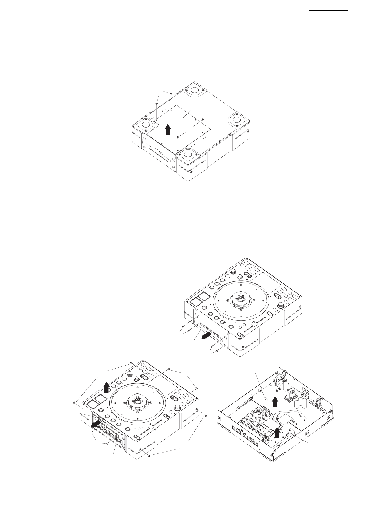
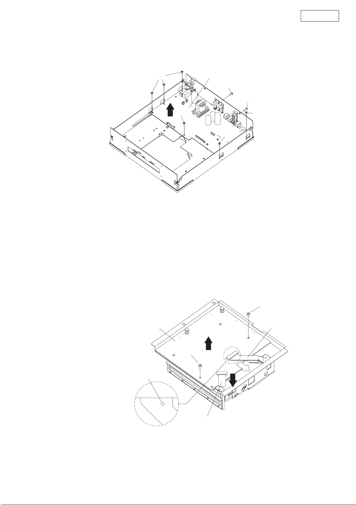
DISASSEMBLY
j
(Follow the procedure below in reverse order when reassembling.)
Note: First of all, remove the Platter. Refer to the Instruction Manuals.
1. Bottom Plate
(1) Remove 4 screws 70 and pull out Bottom Plate.
70
Bottom Plate
70
2. Top Cover unit
(1) Remove 4 screws 71.
(2) Detach FFC ESC.
(3) Remove 2 Push Rivets 31.
(4) Disconnect Connector to remove Eject LED unit.
(5) Remove 6 screws 71.
(6) Disconnect FFC Cable and Connector.
(7) Detach Top Cover unit.
DN-S3500
71
Front ESC
71
Connector
CW121
Connector
CX032
71
31
E
ect LED unit
71
71
Note:
z Do not pull out aslant to prevent FFC cable damage.
z Do not fail to pull AC cord from wall outlet before disconnect FFC Cable.
If AC cord is remained plugged into wall outlet, power is kept supplied in the unit, which may cause danger.
3
FFC Cable
CX251
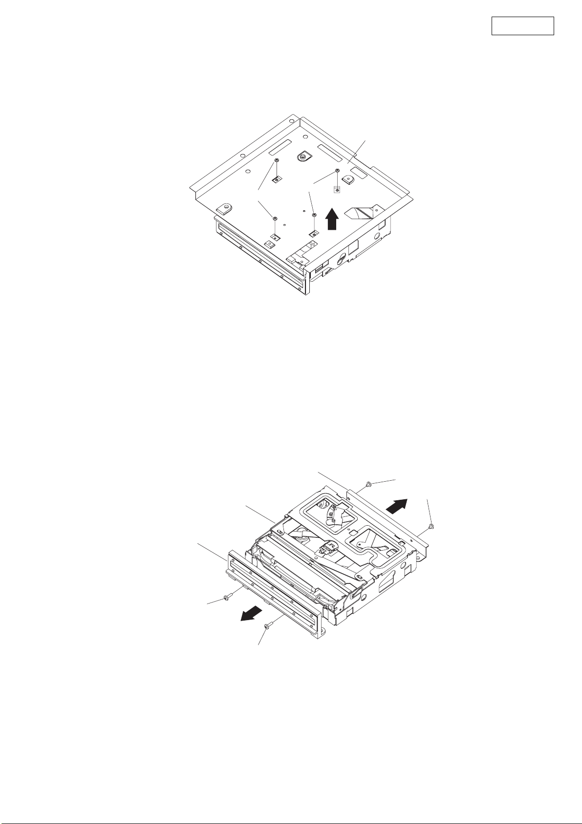
Page 4
3. Motor unit
e
(1) Remove 4 screws 74.
(2) Detach Motor unit (FG3500).
74
DN-S3500
Motor unit
(FG3500)
74
4. Mecha unit
(1) Remove 2 screws 63 and 2 screws 64.
(2) Disconnect FFC cable and Connector.
(3) Detach Mecha Unit.
Mecha unit
Connector
CX061
64
63
63
FFC Cabl
CX361
Note:
z Do not pull out aslant to prevent FFC cable damage.
z Do not fail to pull AC cord from wall outlet before disconnect FFC cable.
If AC cord is remained plugged into wall outlet, power is kept supplied in the unit, which may cause danger.
4
Page 5
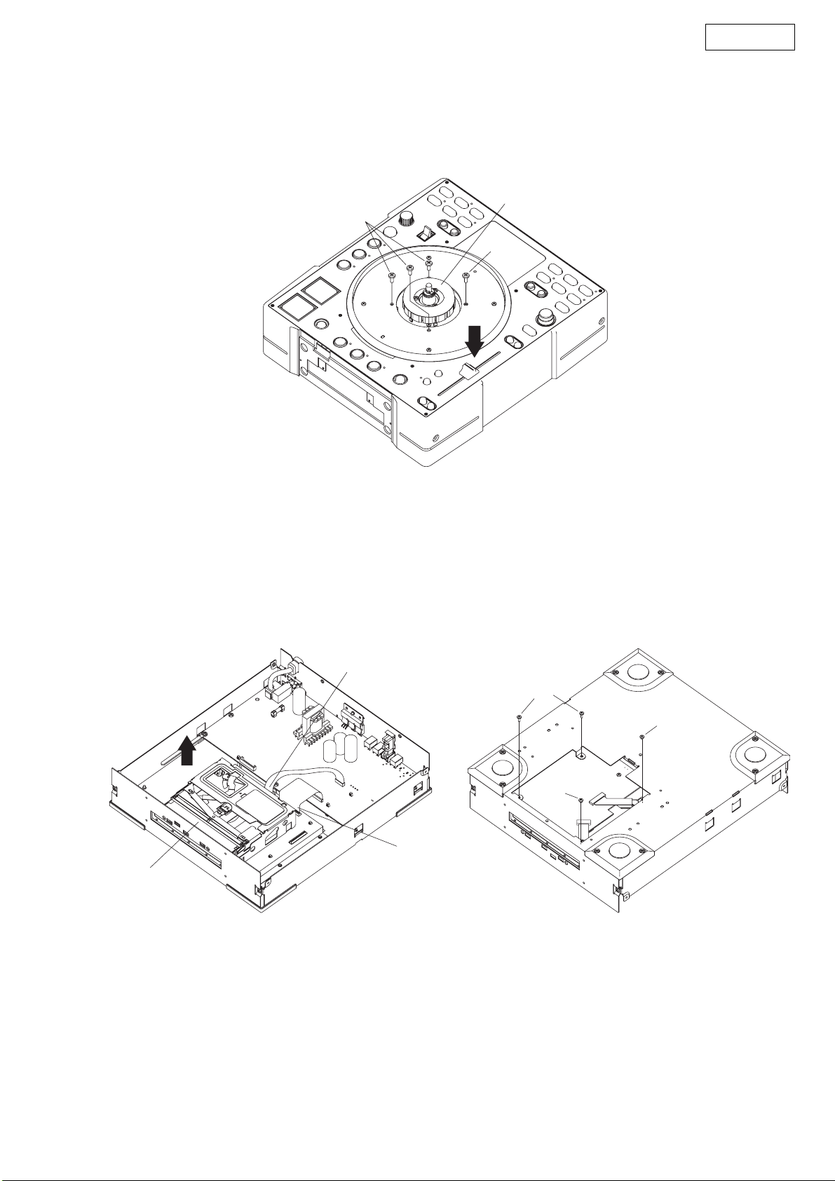
5. Power P.W.B.
(1) Remove 6 screws 69, a screws 72 and a screws 73.
(2) Detach Power P.W.B.
DN-S3500
69
69
Power P.W.B.
73
72
69
69
6. Main P.W.B.
(1) Short-circuit the short land above.
(2) Remove a screws 65 and a screws 66.
(3) Disconnect FFC Cable and FPC Cable.
(4) Detach Main P.W.B.
Main P.W.B.
Short land for laser diode
65
FPC Cable
66
Note:
z Do not pull out aslant to prevent FFC cable damage.
FFC Cable
5
Page 6
7. Shield Plate (E3 Model only)
(1) Remove 4 screws 60.
(2) Detach Shield Plate.
DN-S3500
Shield Plate
60
8. CD Mecha
(1) Remove 2 screws 63 and pull out Main Pwb Bracket.
(2) Remove 2 screws 64 and pull out Disc Guide.
Main Pwb Bracket
CD Mecha
60
63
63
Disc Guide
64
64
6
Page 7
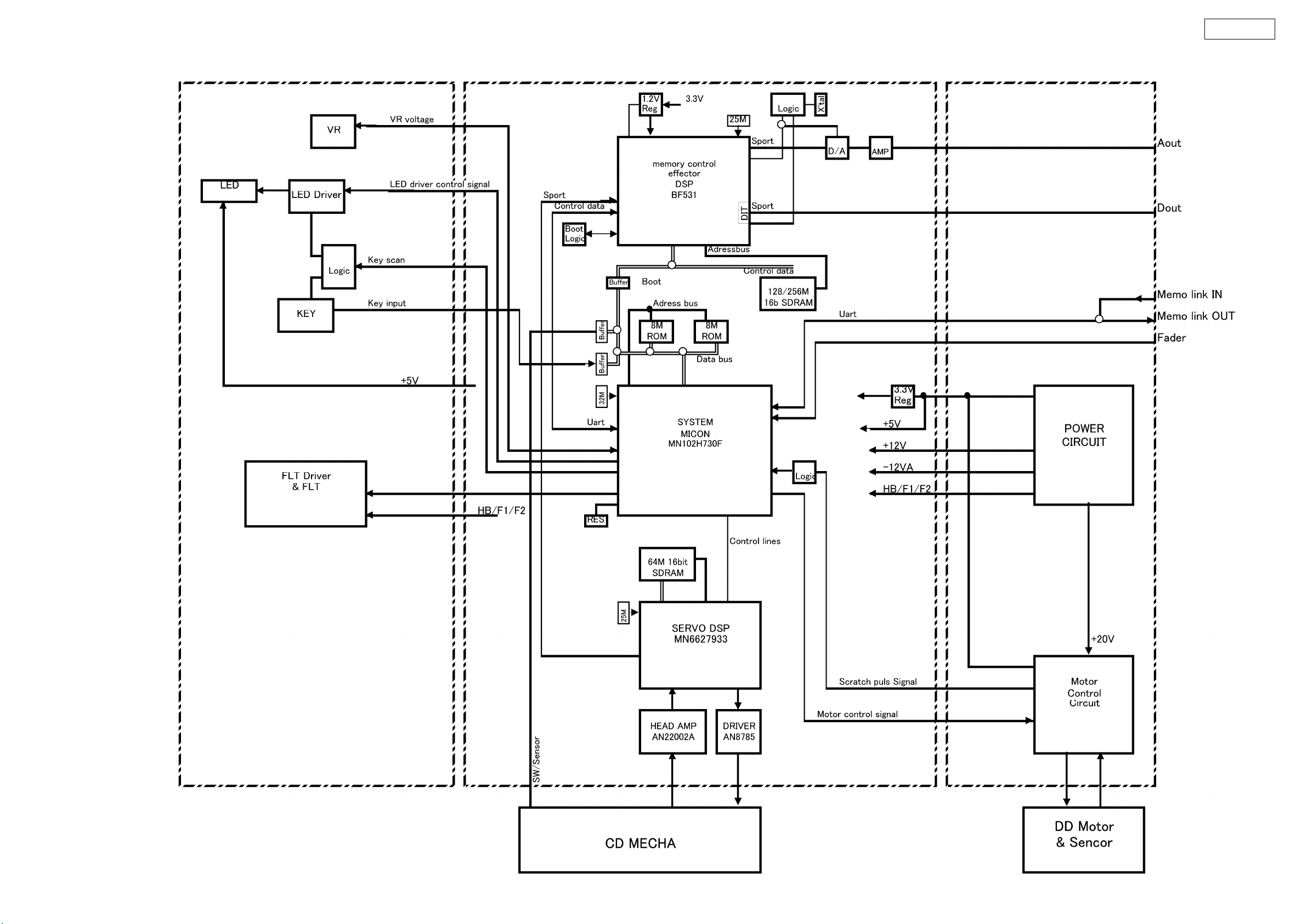
BLOCK DIAGRAM
DN-S3500
7
Page 8
DN-S3500
CONFIRMING THE SERVO
What is Service Program
Service program is a special program intended for confirming servo functions etc.
Required Measuring Implement
Reference disc (TCD784 or CO-74176)
1. Contents of Service Program
Turn on the power while pressing both B button and the PARAMETER knob to set the service mode of DN-S3500. The various
check items can be selected with the PARAMETER knob, the various test items can be selected with the A, SAMP, EXIT/RELOOP,
(SAMP.)EXIT/RELOOP, and BEND buttons. Press either the PARAMETER knob or PLAY/PAUSE button to start the check
or test and display the result.
To eject the disc, press the DISC EJECT button.
To cancel the service mode, turn the power off.
PAR A ME T ER
knob
Process No.
(TRACK
Indication)
01
02
03
04 "Fo_Gain"
05 "Tr_Gain" Select the tracking gain. Default : 2. The operation is the same as for the Fo Gain.
06 "Block_Err" The block error rate is displayed.
07 "PU._Clean"
08
09
Function
(Character-display)
µcom Version check
(Version No.)
"TR_Signal"
"HF_Signal"
Automatic Servo
Adjustment call
(Servo Data)
Error Code Check
(Error Data)
Total Running Time
(Total Time)
Contents
A PARAMETER knob is pushed and a version is checked.
1. System µcom version No. : "System_XXXX"
2. DSP soft version No. : "Dsp_XXXX"
Press the PARAMETER knob to turn the tracking servo off.
When the tracking servo is off, press the PARAMETER knob to turn the tracking
servo on.
Press the PARAMETER knob to start automatic servo adjustment. When the
adjustment is completed, the adjustment data is displayed. The data can be
selected by turning the EFFECTS knob.
1. Disc check, CD/CD-RW
2. Focus gain data
3. Focus balance data
4. Focus offset data
5. Tracking gain data
6. Tracking balance data
7. Tracking offset data
8. S curve maximum
9. S curve minimum
Select the focus gain. Default : 7. Select the data with the scratch disc, then press
the PARAMETER knob to enter it. The higher the value, the higher the gain, while
the lower the value, the lower the gain.
* Do not change this without instruction from engineering.
When the PARAMETER knob is pressed, the pickup moves towards the outer
edge of the disc. The pickup lens becomes visible through the slit in the CD mechanism plate. The lens can be cleaned using a cotton swab, etc.
(Perform this operation with the top panel/cover removed and the disc ejected.)
During normal operation, the error code for the error that occurred is displayed.
Turn the EFFECTS knob to select up to 10 sets of error data stored in the memory. (See the error code table for a description of the error codes.)
・Press the PARAMETER knob to set the error data clear mode. ("Error Clear?" is
displayed.) Press the PARAMETER knob again to clear all the error data.
The total operating time of the spindle motor is displayed. A total of 65,535 hours
can be counted, in units of hours.
NOTE: If the power is turned off after 59 minutes or less, that hour is not counted.
・Press the PARAMETER knob to set the total time clear mode. ("Time Clear?" is
displayed.) Press the PARAMETER knob again to clear the total time.
サービスモード
サービスモードについて
サービスモードは、サーボ状態などを確認するための特別なプログラムです。
確認に必要な測定器具
リファレンスディスク:TCD784、CO-74176
1. サービスプログラムの内容
DN-S3500 は B ボタンとパラメータノブを両方押しながら、電源を投入するとサービスモードになります。パラメータノブで各チェック項目が、A ボタン、
SAMP ボタン、EXIT/RELOOP ボタン、(SAMP.)EXIT/RELOOP ボタン、 ボタンまたは BEND ボタンで各テスト項目が選択できます。
パラメータノブを押すか、PLAY/PAUSE ボタンを押すと各項目のチェック、テストを開始し、その結果を表示します。
ディスクをイジェクトするには、DISCEJECT ボタンを押します。
サービスモードをキャンセルするには、電源を切ってください。
パラメータノブ
チェック項No.
( トラック番号 )
01
02
03
04 "FoGain"
05 "TrGain" トラッキングゲインを選択します。デフォルト -2.操作方法は FoGain と同じ。
06 "BlockErr" ブロックエラーレートが表示されます。
07 "PU.Clean"
08
09
マイコンバージョンチェツク
VersionNo
"TRSignal"
"HFSignal"
サーボ自動調整値
読み出し
(ServoData)
エラーコードチェック
(ErrorData)
トータルランニングタイム
(TotalTime)
機能
キャラクター表示
内容
パラメータノブを押して、バージョンをチェックします。
1.システムマイコンバージョン No.:"SystemXXXX"
2.DSP ソフトバージョン No.:"DspXXXX"
パラメータノブを押すとトラッキングサーボを off します。
トラッキングサーボ off のとき、パラメータノブを押すとトラッキングサーボを on します。
パラメータノブを押すとサーボ自動調整を開始します。調整が終了すると、調整データ表示
します。データはエフェクトノブを回すことで選択できます。
1.ディスクチェック、CD/CD-RW
2.フォーカスゲインデータ
3.フォーカスバランスデータ
4.フォーカスオフセットデータ
5.トラッキングゲインデータ
6.トラッキングバランスデータ
7.トラッキングオフセットデータ
8.S カーブ最大値
9.S カーブ最小値
フォーカスゲインを選択します。デフォルト -7。スクラッチディスクでデータを選択し、パラメータノブを押
すと確定されます。数値が大きくなるとゲインが高くなり、数値が小さくなるとゲイン
が低くなります。
*設計からの指示がない限り変更しないで下さい。
パラメータノブを押すとピックアップがディスク外周方向へ移動します。CD メカ板金の隙間から
ピックアップのレンズが見えるようになります。綿棒等でレンズをクリーニングすることができ
ます。
( トップパネル / カバーを外し、ディスクをイジェクトした状態で実施下さい )
通常動作時、発生したエラーのエラーコードが表示されます。エフェクトノブを回すと、最大 10
個まで、記憶されたエラーデータが選択できます。( エラーコードはエラーコード表を参照下さい。)
・パラメータノブを押すと、エラーデータ消去モードになります。(ErrorClear?が表示されま
す ) 再度、パラメータノブを押すと、全てのエラーデータが消去されます。
スピンドルモータのトータル動作時間を表示します。1 時間単位で 65535 時間まで計測でき
ます。注意 )59 分以下で電源を切るとカウントされません。
・パラメータノブを押すと、トータル時間消去モードになります。(TimeClear?が表示されま
す ) 再度、パラメータノブを押すと、トータル時間が消去されます。
8
Page 9
DN-S3500
BEND+ button FLT all light check performed while button pressed.
-
BEND
button FLT all off check performed while button pressed.
button Disc eject status set while button pressed.
The disc loading/eject roller turns. The dirt can be cleaned off the roller by gently pressing a cotton swab with
propyl alcohol"
, against the roller.
(Perform this operation with the top panel/cover removed and the disc ejected.)
Servo automatic adjustment read-out value
Adjustment Item Adjustment Value indication at character portions.
1 Focus Gain 0408 ~ 3248
2 Focus Balance -50 ~ +50
3 Focus Offset -005 ~ +005
4 Tracking Gain 0392 ~ 1569
5 Tracking Balance -025 ~ +025
6 Tracking Offset -005 ~ +005
2. TEST MODE
A button
A2 button
SAMP button
(SAMP.)EXIT
/RELOOP
button
EXIT/
RELOOP
button
Function
(Character-display)
Heat Run Test
H/R1 Normal
Chucking Test
H/R2 Tray
Platter rotation speed
check
Platter rotation speed
fine adjustment
System check
Sys. Check
Press button A1, then press the PLAY/PAUSE button to start the test.
The disc is ejected, loaded and played repeatedly.
For discs containing 20 tracks or less, all the tracks are played.
For discs containing 21 tracks or more, only the first and last tracks on the disc are played.
If an error occurs, the error code is displayed and the stop mode is set.
Press button A2, then press the PLAY/PAUSE button to start the test.
The disc load/eject, servo input and TOC reading operations are performed repeatedly.
If an error occurs, the error code is displayed and the stop mode is set.
Press button SAMP, then press the PLAY/PAUSE button. The platter starts to rotate and
revolution number is displayed.
Press the (SAMP.)EXIT/RELOOP button, then press the PLAY/PAUSE button. The Platter starts
to rotate and revolution number is displayed. The rotation speed can be adjusted to turn the
parameter knob.
Press button EXIT/RELOOP, then press the PLAY/PAUSE button to start the system check.
Once the check is completed, the results are displayed.
1. The system µcom and DSP communications are checked.
2. Reading and writing SDRAM of DSP are checked.
3. Reading and writing SDRAM of servo DSP are checked.
4. Communications between the system µcom and servo DSP are checked.
5. The CD drive operation is checked. (Inner edge switch detection is performed.)
6. The CD drive operation is checked. (Disc detection is performed.)
Once all the checks are completed, the results are displayed on the character display. The
numbers of the checks in items 1 to 6 above that were OK are displayed. If one of the checks
was not OK, the number of that item is not displayed.
Contents
3. Error Code Table (Appears only at Heat Run and Chucking Test function)
Error Code Contents
Automatic Adjustment Error
E1 00
E1 01
E1 03
E1 04
E1 05
E1 06
E2 02 Servo down during automatic Adjustment
E3 00 Unable to read TOC
Unable to detect disk
Unable to adjust tracking offset
Unable to adjust focus fine gain
Unable to actuate focus
Unable to actuate tracking
Unable to adjust tracking fine gain
"Iso-
BEND+ボタン ボタンを押している間、FLT の全点灯チェックを行います。
-
BEND
ボタン ボタンを押している間、FLT の全消灯チェックを行います。
ボタン ボタンを押している間、ディスクをイジェクト状態にします。
ディスクローディング / イジェクト用のローラーが回転しますので、イソプロピルアルコールを付けた綿棒をローラーに軽く押し当てることに
より、ローラーの汚れを落とすことができます。
( トップパネル / カバーを外し、ディスクをイジェクトした状態で実施下さい )
サーボ自動調整読み出し値
サーボ調整項目 調整 OK 範囲
1 フォーカスゲイン 0408 〜 3248
2 フォーカスバランス -50 〜 +50
3 フォーカスオフセット -005 〜 +005
4 トラッキングゲイン 0392 〜 1569
5 トラッキングバランス -025 〜 +025
6 トラッキングオフセット -005 〜 +005
2. テストモード
機能キャラクター表示 内容
A1 ボタンを押し、PLAY/PAUSE ボタンを押すとテストを開始します。
ディスクの出し入れと、再生を繰り返します。
20 トラック以下のディスクのときは、全てのトラックを再生します。
21 トラック以上のディスクのときは、ディスク先頭トラックと最終トラックのみ再生します。エラーが発生すると、エラーコード
を表示して停止します。
A2 ボタンを押し、PLAY/PAUSE ボタンを押すとテストを開始します。
ディスクの出し入れと、サーボ投入、TOC の読み込みを繰り返します。
エラーが発生すると、エラーコードを表示して停止します。
SAMP ボタンを押し、PLAY/PAUSE ボタンを押すとプラッターが回転し、プラッターの回転数を表示します。
(SAMP.)EXIT/RELOOP ボタンを押し、PLAY/PAUSE ボタンを押すと、プラッターが回転し、プラッターの回転速度
を表示します。パラメータノブを回すと調整することができます。
EXIT/RELOOP ボタンを押し、PLAY/PAUSE ボタンを押すとシステムチェックを開始し、チェック終了後、その結果を表
示します。
1.システムマイコンと DSP の通信チェツクを行います。
2.DSP の SDRAM のリード / ライトチェツクを行います。
3.サーボ DSP の SDRAM のリード / ライトチェツクを行います。
4.システムマイコンとサーボ DSP の通信チェツクを行います。
5.CD ドライブの動作チェックを行います。( 内周 SW の検出をおこないます。)
6.CD ドライブの動作チェックを行います。( ディスク検出をおこないます。)
全てのチェックが終了すると、キャラクター表示に結果を表示します。1 〜 6 項目のチェックが OK の時は、OK になっ
た項目の番号が表示されます。NG の項目が合った場合、NG になった項目の番号が表示されません。
Aボタン
A2 ボタン
SAMP ボタン
(SAMP.)EXIT/
RELOOP ボタン
EXIT/RELOOP
ボタン
ヒートランテスト
H/R1Normal
チャッキングテスト
H/R2Load
プラッター回転速度
チェック
プラッター回転速度
微調整
システムチェック
Sys.Check
3. エラーコードテーブル ( ヒートランテスト、及び、チャッキングテストのとき表示されます )
エラーコード 内容
サーボ自動調整エラー
E100
E101
E103
E104
E105
E106
E202 サーボ自動調整中サーボが外れた。
E300 TOC が規定時間内に読めない。
ディスクが検出できない。
トラッキングオフセットが調整できない。
フォーカスゲインが調整できない。
フォーカスサーボが入らない。
トラッキングサーボが入らない。
トラッキングゲインが調整できない。
9
Page 10
DN-S3500
Error Code Contents
E4 00
E4 01
E5 00
E5 01
E5 02
E8 00 Track jumping was happened during memory of data. And unable to memorize data continuously.
TR MIN SEC FRAM CHARACTER
displays the track No. in
which error occurred.
Unable to close the disc holder in the regular time
Unable to open the disc holder in the regular time
The inner SW dose not turn on
Slider error
The inner SW dose not turn off
Error Indication
Displays the time at which error occurred.
H ****Operation count
E ****Error code
4. µcom update
The system µcom and DSP can be updated from a disc.
The µcom should be updated to the latest version, when GU-3689(MAIN PWB UNIT) or IC102(Flash ROM) is replaced.
(1) Creating the update disc
Use the procedure described below to create the disc for updating the system microprocessor and DSP.
① Store the update file on a CD-R or CD-RW disc in ISO9660 Mode 1 format, then finalize the disc.
・Write the distributed update files using the "DISC AT ONCE" CD writing software and finalize.
・Do not record any other software or data on the disc containing the update software.
・Do not change the file names - use the file names as distributed.
エラーコード 内容
E400
E401
E500
E501
E502
E800 メモリにデータ記憶中トラック飛びが発生し、規定のリトライを実施したが、連続でデータ記憶出来なかった。
トラック 分 秒 フレーム キャラクター
エラーが発生したトラック番号 エラーが発生した時間 (A タイム ) H ****動作回数
ディスクが規定時間内にローディングできない。
ディスクが規定時間内にイジェクトできない。
内周 SWON しない
スライドエラー
内周 SWOFF しない
エラー表示
E ****エラーコード
4. マイコンアップデート
DN-S3500 は、ディスクから、システムマイコン、DSP のアップデートを行うことができます。
GU-3689( メイン基板ユニット ) 又は、IC102 を交換した時は、最新バージョンにアップデートしてください。
(1) アップデートディスクの作成
システムマイコン、DSP のアップデート用ディスクディスクを下記に従い作成する。
① アップデート用のファイルを、CD-R、又は CD-RW ディスクに ISO9660,MODE1 のフォーマットで記録し、ファイナライズする。
・配布されたアップデートファイルを、CD ライティングソフトで DISCATONCE で書き込みしファイナライズする。
・アップデート用ソフト以外のソフトやデータを同一ディスク内に記録しないこと。
・ファイル名は、配布されたときのファイル名をそのまま使用すること。
(2) Updating the system µcom and DSP
① Turn on the power and load the disc created in (1) above.
When the update disc is detected, "Version Up" is displayed. And "xxxx → yyyyy" and "Push Play!" are displayed by turns.
xxxx : Old Version No., yyyy : New Version No.
② Press the PLAY/PAUSE button. "NowLoading" is displayed and the updating procedure starts.
As updating proceeds, the playback position indicator lights in order from left to right.
NOTE: In some extremely rare cases, the updating procedure is not completed. If the updating procedure has not finished after
three minutes, there could be a problem. Turn off the power and repeat the operation from step (2) ① .
Depending on the problem that occurred, it may happen that no other operations can be performed. If this happens, GU-
3689 IC102 must be replaced. Software must be pre-recorded on the IC102. (When ordering the IC102, order the more
recent system microprocessor version number (GEN number).)
③ When updating is completed, "Complete!" is displayed and the disc is ejected.
ADJUSTMENT
* When the motor (FG-3500) is replaced, platter rotation speed adjustment is necessary.
(1) Start the Platter Rotation Speed Fine Adjust mode in the test mode. (Refer to page 9)
The actual revolution number is indicated on the lower part of the Character display. (Standard is 33rpm)
The difference from the standard revolution number is indicated on the upper part of the Character display.
(2) Turn the parameter knob. And the "D_**"(left side) of the lower part of the Character display is set to "D_77".
Then check the difference from the standard revolution number.
-
a) The difference from the standard number is
・Turn the parameter knob to set "-2%". And push the parameter knob to complete the adjustment.
b) The difference from the standard number is outside of
・Start the platter revolution check mode in the test mode. (Refer to page 9)
Present revolution number is indicated on the lower part of character display. (Standard is 33rpm)
Difference from the standard revolution number is indicated on the upper part of character display.
・Make adjustment by turning VR701 on the power unit GU-3690 so that difference from the standard revolution number
indicated on the upper part of character display becomes
5% ~ +1% :
-
5% ~ +1% :
-
2%.
(2) システムマイコン、DSP のアップデート
① 電源を投入し、(1) で作成したディスクをローディングします
アップデート用ディスクが検出されると、"VersionUp" と表示し、"xxxx → yyyy"、"PushPlay!" の交互表示になります。
xxxx:旧バージョン No.、yyyy:新バージョン No.
② PLAY/PAUSE ボタンを押すと、"NowLoading" を表示しアップデートを開始します。
アップデートの進行に合わせ、再生位置表示が左から右へ順に点灯します。
注意 ) 大変希ではありますが、アップデート中に、アップデート未終了の異常状態が発生することがあります。アップデートを開始し3分
を経過しても終了しない場合も、異常が発生したと考えられますので、電源を切って、再度、(2) ①から同一の操作を
行って下さい。
発生した異常状況により、以後の全ての動作が出来なくなることがあります。その場合、GU-3689IC102 の交換が必要
になります。IC102 は、予め、ソフトウエアを書き込みする必要があります。(IC102 を発注の際は、最新のシステム
マイコンバージョン No(GENNo) で発注願います。)
③ アップデートが終了すると、"Complete!" を表示しディスクがイジェクトされます。
調整
*モータユニット(FG-3500) を交換した時は、プラッターの回転速度の調整が必要です。
(1) テストモードのプラッター回転速度微調整モードをスタートさせる。(9 ページ参照 )
キャラクター表示部下段の右側に現在の回転数が表示されます。( 基準は、33rpm です。)
キャラクター表示部上段に基準回転数との差が表示されます。
(2) パラメータノブを回し、キャラクター表示下段左側の D** を D77 に設定します。
その時、基準回転数との差を確認します。
-
a) 基準回転数との差が
・パラメータノブを回して、基準回転数との差が
が確定します。
b) 基準回転数との差が
・テストモードのプラッター回転数チェックモードをスタートさせる。(9 ページ参照 )
キャラクター表示部下段に現在の回転数が表示されます。( 基準は 33rpm です。)
キャラクター表示部上段に基準回転数との差が表示されます。
・電源ユニット GU-3690 の VR701 を回し、キャラクター表示部上段に表示されている基準回転数との差が
ます。
5%〜+1% の場合:
-
2%になるように調整する。そして、パラメータノブを押すと、回転速度の調整
-
5%〜+1% の範囲から外れる場合:
-
2% になる様に調整し
10
Page 11
SEMICONDUCTORS /半導体一覧表
Only major semiconductors are shown, general semiconductors etc. are omitted to list.
主な半導体を記載しています。汎用の半導体は記載を省略しています。
1. IC’s
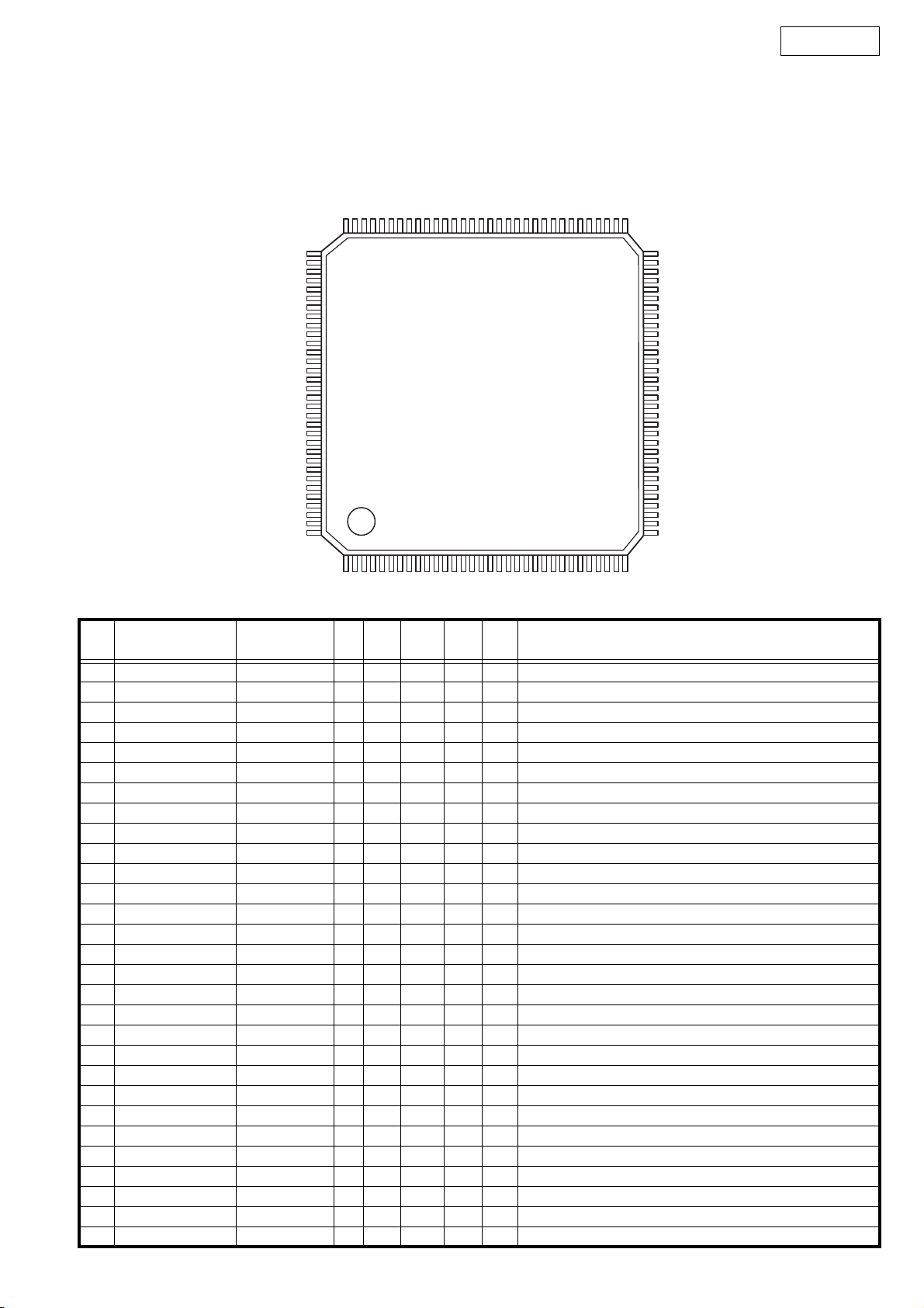
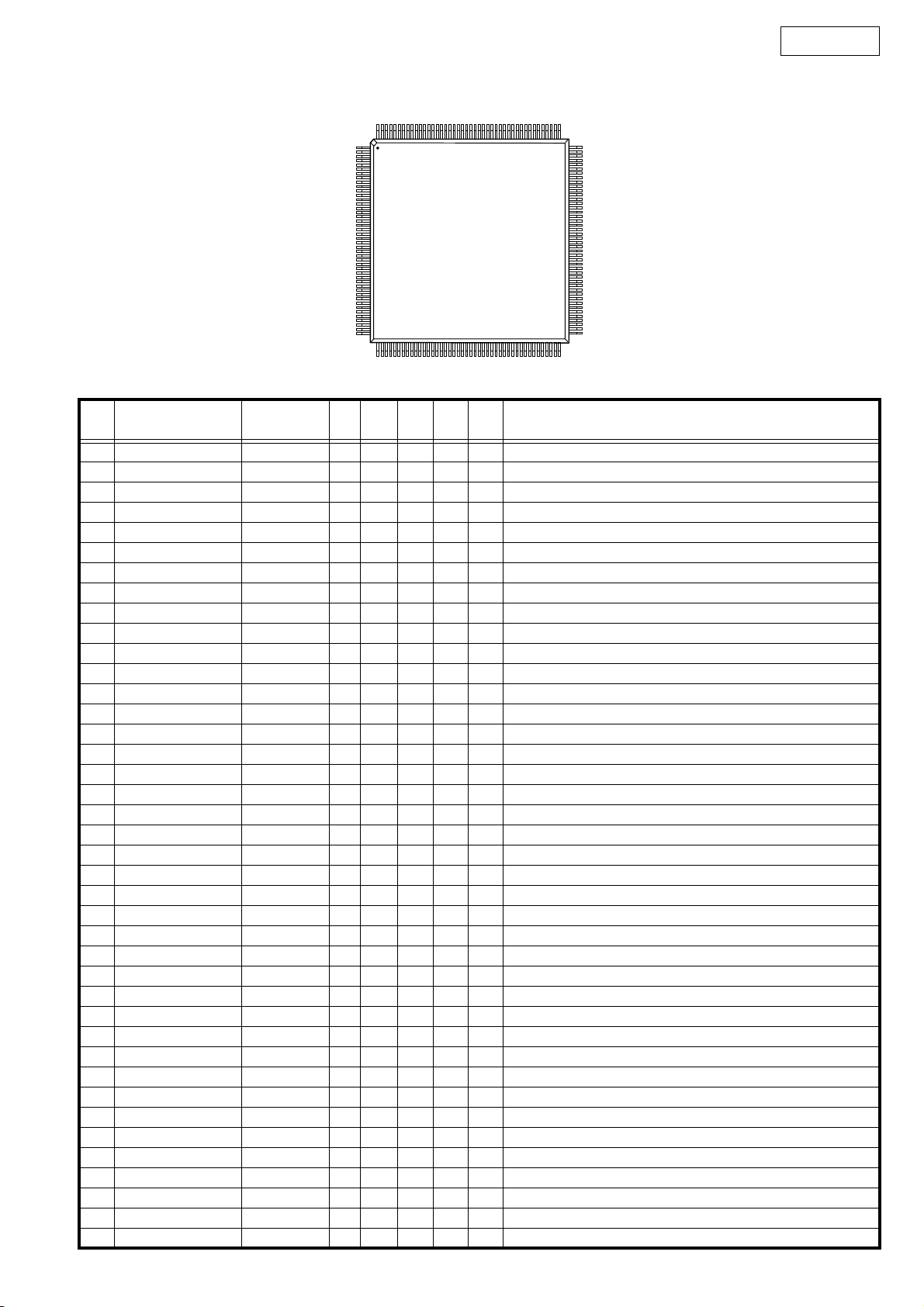
MN102H730F (IC101)
96 65
97 64
TOP VIEW
DN-S3500
128 33
1
32
MN102H730F Terminal Function
Pin
No.
1 CS0_ CS0_ O - Pu - - External memory chip select 0 (FrashROM CS)
2 CS1_ CS1_ O - Pu - - External memory chip select 1 (Frashrom for memo)
3 D00 DQ0 I/O - - - - External memory data in/out 0, DSP interface 0
4 D01 DQ1 I/O - - - - External memory data in/out 1, DSP interface 1
5 D02 DQ2 I/O - - - - External memory data in/out 2, DSP interface 2
6 D03 DQ3 I/O - - - - External memory data in/out 3, DSP interface 3
7 VDD VDD - - - - - Power (+3.3V)
8 VSS VSS - - - - - GND
9 D04 DQ4 I/O - - - - External memory data in/out 4, DSP interface 4
10 D05 DQ5 I/O - - - - External memory data in/out 5, DSP interface 5
11 D06 DQ6 I/O - - - - External memory data in/out 6, DSP interface 6
12 D07 DQ7 I/O - - - - External memory data in/out 7, DSP interface 7
13 D08 DQ8 I/O - - - - External memory data in/out 8, DSP interface 8
14 D09 DQ9 I/O - - - - External memory data in/out 9, DSP interface 9
15 D10 DQ10 I/O - - - - External memory data in/out 10, DSP interface 10
16 PD0,DMAACK1_ MUTE_ O - Pd L L Mute signal (L:mute)
17 PD1,DMAREQ1_ DSPF3 O - - L - FLAG3 for DSP
18 D11 DQ11 I/O - - - - External memory data in/out 11, DSP interface 11
19 D12 DQ12 I/O - - - - External memory data in/out 12, DSP interface 12
20 D13 DQ13 I/O - - - - External memory data in/out 13, DSP interface 13
21 D14 DQ14 I/O - - - - External memory data in/out 14, DSP interface 14
22 D15 DQ15 I/O - - - - External memory data in/out 15, DSP interface 15
23 WORD WORD I - - Data bus width select (H:16bit width), GND fixed
24 VDD VDD - - - - - Power (+3.3V)
25 MODE MODE I - - L L Processor mode, GND fixed
26 PC3 APOWER O - Pd L L Analog out power ON/OFF (L: Power OFF)
27 XI XI I - - - - Oscillation input terninal
28 XO XO O - - - - Oscillation output terninal
29 VDD VDD - - - - - Power (+3.3V)
Pin Name Symbol I/O DET Ext Ini Res Function
11
Page 12
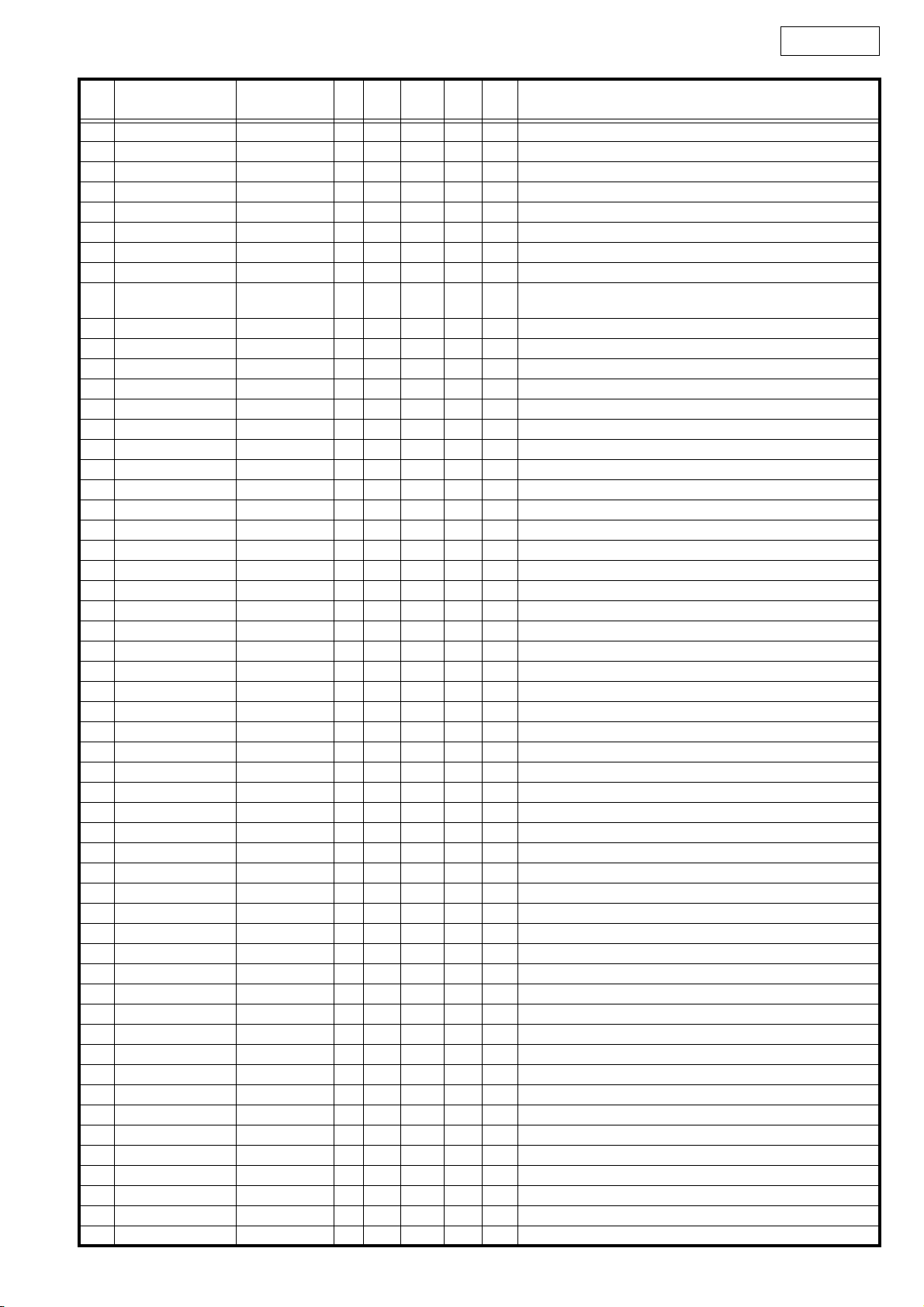
DN-S3500
Pin
No.
30 OSCI OSCI I - - - - Oscillation input terninal 32.0MHz
31 OSCO OSCO O - - - - Oscillation output terninal
32 VSS VSS - - - - - GND
33 P57,BOSC DR_/W O - - H - DN7000X: DSP interface send/receive select signal
34 PC5,NMI_ NMI I - - - - Connect to power
35 RST_ RST_ I - - - - Micro-processor RESET
36 PC0 FPLAY1 I - (Pu) H H MAIN fader start PLAY input
37 P76 FCUE1 I - (Pu) H H MAIN fader start CUE input
38 P60,IRQ0 DTIME I - iPu H -
39 P61,IRQ1 BLKCK I - iPu - - Sub-code clock interrupt
40 P62,IRQ2,TM10IOA TABLE I - (Pu) - - Pulse width measure input for turntable
41 P63,IRQ3,TM10IOB DBCLK I - - - - Pulse width measure clock input (5.6MHz) for DISC
42 P64,IRQ4 DTIMES I - iPu H - X2;clock interrupt input for sampler play/X1
43 P65,IRQ5,TM12IOA DISCA I - - - - Pulse width measure input for scratch DISC
44 P66,IRQ6 DISCDIR I - (Pu) - - Scratch DISC turn direction detect interrupt input
45 P67,IRQ7 DQSY I - iPu - - CD-TEXT DQSY interrupt
46 P70,TM13IOB DISCPA I - (Pu) H H Pulse A count input for scratch DISC
47 P71 ML O - iPu - - D/A interface latch 2 lines common
48 PD2,DMAACK0_ CHGOFT O - - L - Off track signal (transistor drive)
49 PD3,TM3IO DISCPA_ I - - - - Pulse A inverse count input for scratch DISC
50 VDD VDD - - - - - Power (+3.3V)
51 P77 DSTBY_ O - Pd L L Driver standby signal Çk: standby
52 P72,TM14IOB DISCPB I - - - - Pulse B count input for scratch DISC
53 P73,TM11I0B DISCINT I - (Pu) - - DISC rotation start interrupt input
54 P74 MLD O - - H - Servo DSP interface latch
55 P75§TM12IOB DBCLK I - - - - Pulse width measure clock input (5.6MHz) for DISC
56 PA0,SBI0 STAT I - iPu - - Servo DSP interface receive (clock synchronous)
57 PA1,SBO0 MDAT O - - H - Servo DSP interface send (clock synchronous)
58 PA2,SBT0 MCLK O - - H - Servo DSP interface clock (clock synchronous)
59 PA3,SBI1 RXDM I - (Pu) - - Interface receive with Memo link SET (asynchronous)
60 PA4,SBO1 TXDM O - Pu H H Interface receive with Memo link SET (asynchronous)
61 PA5,SBT1 NRES_ O - Pd L L Peripheral IC reset signal
62 PB0,SBI2 DSPRXD I - Pu - H DSP interface receive (asynchronous)
63 PB1,SBO2 DSPTXD O - Pu H H DSP interface send (asynchronous)
64 PB2,SBT2 FLCS_ O - - H - FLT driver enable signal
65 PB3,SBI3 FLRES_ O - Pd L L FLT driver reset signal
66 PB4,SBO3 PDATA O - - H - FLT driver data, and LED driver data (clock synchronous)
67 PB5,SBT3 FLCLK O - - H - FLT driver data send clock (clock synchronous)
68 VDD VDD - - - - - Power (+3.3V)
69 VSS VSS - - - - - GND
70 AVSS AVSS - - - - - Analog standard GND for AD conversion
71 Vref- Vref- - - - - - Analog standard voltage for AD conversion
72 P80 O - Pd L L Not used
73 P81 O - - H - Not used
74 P82 O - - H - Not used
75 P83 SEL_A O - - L - Key scan out select signal A
76 P84 SEL_B O - - L - Key scan out select signal B
77 P85 SEL_C O - - L - Key scan out select signal C
78 P86,AD06 PITCH I - - - - Slide VR data input for pitch
79 P87,AD07 PITCHC I - - - - Slide VR center value data input for pitch
80 PD4 SEL_D O - Pu H H Key scan out select signal D
81 PD5 I - Pu (H) H Not used
82 P90 I - Pu (H) H Not used
83 P91 MSTART O - Pd L L MOTOR START/STOP H: MOTOR START
84 P92 MDIR O - - H - MOTOR turn direction select H: forward
Pin Name Symbol I/O DET Ext Ini Res Function
X2;clock interrupt in for play/X1;LRCK :used for time code make
out when MP3 play
12
Page 13
DN-S3500
Pin
No.
85 P93 DSPRES_ O - Pd L L DSP RESET signal L: RESET
86 Vref+ Vref+ - - - - - Analog standard voltage +3.3V for AD conversion
87 AVDD AVDD - - - - - Power (+3.3V)
88 P94,DAC0 MSPD1 O - - - - MOTOR turn speed output D/A1
89 P95,DAC1 MSPD2 O - - - - MOTOR turn speed output D/A2(RESERVE)
90 P96,DAC2 MBRK O - - - - MOTOR BRAKE ON: H
91 P97,DAC3 LOAD O - - - - Disc loading, eject signal (D/A)
92 PC6,BREQ_ BREQ_ I - Pu - H Bus request signal
93 PC7,BRACK_ BRACK_ O - Pu H H Bus request accept signal
94 WEL_ WE_ O - Pu - H External memory write enable (lower 8bit)
95 P51 BOOT_ O - Pu H H DSP boot start signal L: START
96 RE_ RE_ O - Pu - H External memory read enable
97 CS2_ CS2_ O - Pu - H External memory chip select 2 (DSP Latch buffer interface)
98 VDD VDD - - - - - Power (+3.3V)
99 VSS VSS - - - - - GND
100 P54,BSTRE DACK_ I - Pu H H Not used
101 P55,WR_ DREQ_ O - Pu H H Not used
102 CS3_ CS3_ O - Pu - H Extended port chip select
103 A00 A00 O - - - - External memory address bus 0 (not used when 16bit bus select)
104 A01 A01 O - - - - External memory address bus 1
105 A02 A02 O - - - - External memory address bus 2
106 A03 A03 O - - - - External memory address bus 3
107 A04 A04 O - - - - External memory address bus 4
108 A05 A05 O - - - - External memory address bus 5
109 A06 A06 O - - - - External memory address bus 6
110 A07 A07 O - - - - External memory address bus 7
111 A08 A08 O - - - - External memory address bus 8
112 PD6 DSPF1 O - - L - FLAG1 for DSP
113 PD7,TM7IO DISCPB_ I - iPu - - Pulse B inverse count input for scratch DISC
114 A09 A09 O - - - - External memory address bus 9
115 A10 A10 O - - - - External memory address bus 10
116 A11 A11 O - - - - External memory address bus 11
117 A12 A12 O - - - - External memory address bus 12
118 A13 A13 O - - - - External memory address bus 13
119 VDD VDD - - - - - Power (+3.3V)
120 PC4 DSPF2 O - - L - FLAG2 for DSP
121 A14 A14 O - - - - External memory address bus 14
122 A15 A15 O - - - - External memory address bus 15
123 A16 A16 O - - - - External memory address bus 16
124 A17 A17 O - - - - External memory address bus 17
125 A18 A18 O - - - - External memory address bus 18
126 A19 A19 O - Pd - - External memory address bus 19
127 A20 A20 O - - - - External memory address bus 20
128 A21 A21 O - - - - External memory address bus 21
Pin Name Symbol I/O DET Ext Ini Res Function
13
Page 14
ADSP-BF531 (IC401)
DN-S3500
176
1
PIN 1
TOP VIEW
44
45
133
88
132
89
ADSP-BF531 Terminal Function
Pin
No.
1 GND GND - - - - - GND
2 GND GND - - - - - GND
3 GND GND - - - - - GND
4 VROUT2 O - - - - External FET drive output 2
5 VROUT1 VROUT1 O - - - - External FET drive output 1
6 VDDEXT VDDEXT I - - - - I/O power (+3.3V)
7 GND GND - - - - - GND
8 GND GND - - - - - GND
9 GND GND - - - - - GND
10 CLKIN CLKIN I - - - - Clock input 25MHz oscillation
11 XTAL XTAL O - - - - Cristal oscillator terminal
12 VDDEXT VDDEXT I - - - - I/O power (+3.3V)
13 _RESET _RESET I - - - - Reset signal input
14 NMI NMI I - - - - Mask disable interrupt
15 GND GND - - - - - GND
16 RTXO O - - - - RTC cristal oscillator output
17 RTXI I - - L L RTC cristal oscillator input
18 VDDRTC VDDRTC I - - - - Real time clock power (+3.3V)
19 GND GND - - - - - GND
20 VDDEXT VDDEXT I - - - - I/O power (+3.3V)
21 PPI_CLK I - - L L PPI clock
22 PPI0 O - - L - PPI data 0
23 PPI1 O - - L - PPI data 1
24 PPI2 O - - L - PPI data 2
25 VDDINT VDDINT I - - - - Internal power (+1.2V)
26 PPI3 O - - L - PPI data 3
27 PF15 O - - L - Programmable flag pin 15
28 PF14 O - - L - Programmable flag pin 14
29 PF13 O - - L - Programmable flag pin 13
30 GND GND - - - - - GND
31 VDDEXT VDDEXT I - - - - I/O power (+3.3V)
32 PF12 I - Pu H H Not used
33 PF11 I - - L - Not used
34 PF10 O - Pu H H Not used
35 PF9 I - Pu H H Not used
36 PF8 DSPF5 O - - L - (RESERVE)
37 PF7 O - - L - Not used
38 PF6 DTIMES O - - L - Playback clock output for SAMPLER
39 GND GND - - - - - GND
40 GND GND - - - - - GND
Pin Name Symbol I/O DET Ext Ini Res Function
14
Page 15

DN-S3500
Pin
No.
41 GND GND - - - - - GND
42 GND GND - - - - - GND
43 GND GND - - - - - GND
44 GND GND - - - - - GND
45 VDDEXT VDDEXT I - - - - I/O power (+3.3V)
46 PF5 DSPF3 O - - L - Programmable flag pin5 Inter micro processor pin3 (RESERVE)
47 PF4 DSPF2 O - - L - Programmable flag pin4 Inter micro processor pin2 (RESERVE)
48 PF3 DSPF1 O - - L - Programmable flag pin3 Inter micro processor pin1 (RESERVE)
49 PF2 DSPF0 O - - L - Programmable flag pin2 Inter micro processor pin0 (RESERVE)
50 PF1 DTIME O - - L - Programmable flag pin1 Clock output for playback
51 PF0 BTEND O - Pd L L Programmable flag pin0 'H' when all boot completed
52 VDDINT VDDINT I - - - - Internal power (+1.2V)
53 SCK O - - L - Master slave clock
54 MISO O - - L - Master input slave output
55 MOSI O - - L - Master output slave input
56 GND GND - - - - - GND
57 VDDEXT VDDEXT I - - - - I/O power (+3.3V)
58 DT1SEC O - - - - Not used
59 DT1PRI DDATA1 O - - - - Main digital out data send 0 (serial port OUT 1)
60 TFS1 DLRCK I - IPu - H Digital out send frame synchro (LRCK) signal (serial port OUT 1)
61 TSCLK1 DBCK I - - - - Digital out send frame synchro (BCK) signal (serial port OUT 1)
62 DR1SEC I - - L L Playback data receive 1
63 DR1PRI I - - - - Not used
64 RFS1 O - - - - Not used
65 RSCLK1 O - IPu - H Not used
66 VDDINT VDDINT I - - - - Internal power (+1.2V)
67 DT0SEC ADATA2 O - - - - Not used
68 DT0PRI ADATA1 O - - - - Main analog playback data send 0 (serial port OUT 0)
69 TFS0 ALRCK I - IPu - H
70 GND GND - - - - - GND
71 VDDEXT VDDEXT I - - - - I/O power (+3.3V)
72 TSCLK0 ABCK I - - - -
73 DR0SEC I - - L L Playback data receive 1
74 DR0PRI SRDATA I - - - - Playback data receive 0 (serial port IN 0)
75 RFS0 LRCK I - - - - Receive frame synchro (LRCK) signal (serial port IN 0)
76 RSCLK0 BCLK I - IPu - H Receive frame synchro (BCK) signal (serial port IN 0)
77 TMR2 O - - L - Timer 2
78 TMR1 O - - L - Timer 1
79 TMR0 O - - L - Timer 0
80 VDDINT VDDINT I - - - - Internal power (+1.2V)
81 TX TX O - Pu H - UART send
82 RX RX I - Pu - H UART receive
83 _EMU _EMU O - - - - Emulation status
84 _TRST _TRST I - Pd - L Test reset (JTAG)
85 TMS TMS I - Pu - H Test mode select (JTAG)
86 TDI TDI I - Pu - H Test data input (JTAG)
87 TD0 TD0 O - - - - Test data output (JTAG)
88 GND GND - - - - - GND
89 GND GND - - - - - GND
90 GND GND - - - - - GND
91 GND GND - - - - - GND
92 GND GND - - - - - GND
93 VDDEXT VDDEXT I - - - - I/O power (+3.3V)
94 TCK TCK I - Pu - H Test clock (JTAG)
95 BMODE1 BMODE1 I - - - - Boot mode strap 1
Pin Name Symbol I/O DET Ext Ini Res Function
Analog playback send frame synchro (LRCK) signal (serial port OUT 0)
Analog playback send frame synchro (BCK) signal (serial port OUT 0)
15
Page 16
DN-S3500
Pin
No.
96 BMODE0 BMODE0 I - - - - Boot mode strap 0
97 GND GND - - - - - GND
98 DATA15 D15 I/O - - - - External bus data 15
99 DATA14 D14 I/O - - - - External bus data 14
100 DATA13 D13 I/O - - - - External bus data 13
101 DATA12 D12 I/O - - - - External bus data 12
102 DATA11 D11 I/O - - - - External bus data 11
103 DATA10 D10 I/O - - - - External bus data 10
104 DATA9 D9 I/O - - - - External bus data 9
105 DATA8 D8 I/O - - - - External bus data 8
106 GND GND - - - - - GND
107 VDDEXT VDDEXT I - - - - I/O power (+3.3V)
108 DATA7 D7 I/O - - - - External bus data 7
109 DATA6 D6 I/O - - - - External bus data 6
110 DATA5 D5 I/O - - - - External bus data 5
111 VDDINT VDDINT I - - - - Internal power (+1.2V)
112 DATA4 D4 I/O - - - - External bus data 4
113 DATA3 D3 I/O - - - - External bus data 3
114 DATA2 D2 I/O - - - - External bus data 2
115 DATA1 D1 I/O - - - - External bus data 1
116 DATA0 D0 I/O - - - - External bus data 0
117 GND GND - - - - - GND
118 VDDEXT VDDEXT I - - - - I/O power (+3.3V)
119 _BG O - - - - Bus accept signal
120 _BGH O - - - - Bus accept wait signal
121 ADDR19 BA1 I/O - - - - External bus address 19
122 ADDR18 BA0/ADDR18 I/O - - - - External bus address 18
123 ADDR17 ADDR17 I/O - - - - External bus address 17
124 ADDR16 ADDR16 I/O - - - - External bus address 16
125 ADDR15 ADDR15 I/O - - - - External bus address 15
126 ADDR14 ADDR14 I/O - - - - External bus address 14
127 ADDR13 ADDR13 I/O - - - - External bus address 13
128 GND GND - - - - - GND
129 GND GND - - - - - GND
130 GND GND - - - - - GND
131 GND GND - - - - - GND
132 GND GND - - - - - GND
133 GND GND - - - - - GND
134 VDDEXT VDDEXT I - - - - I/O power (+3.3V)
135 ADDR12 ADDR12 I/O - - - - External bus address 12
136 ADDR11 ADDR11 I/O - - - - External bus address 11
137 ADDR10 ADDR10 I/O - - - - External bus address 10 (SDRAM connects with SDA10)
138 ADDR9 ADDR9 I/O - - - - External bus address 9
139 ADDR8 ADDR8 I/O - - - - External bus address 8
140 ADDR7 ADDR7 I/O - - - - External bus address 7
141 ADDR6 ADDR6 I/O - - - - External bus address 6
142 ADDR5 ADDR5 I/O - - - - External bus address 5
143 VDDINT VDDINT I - - - - Internal power (+1.2V)
144 GND GND - - - - - GND
145 VDDEXT VDDEXT I - - - - I/O power (+3.3V)
146 ADDR4 ADDR4 I/O - - - - External bus address 4
147 ADDR3 ADDR3 I/O - - - - External bus address 3
148 ADDR2 ADDR2 I/O - - - - External bus address 2
149 ADDR1 ADDR1 I/O - - - - External bus address 1
150 _ABE1 SDQM1 I/O - - - - SDRAM data mask 1
Pin Name Symbol I/O DET Ext Ini Res Function
16
Page 17
DN-S3500
Pin
No.
151 _ABE0 SDQM0 I/O - - - - SDRAM data mask 0
152 _AWE _AWE O - - H H Asynchro memory write enable
153 _ARE _ARE O - - H H Asynchro memory read enable
154 _AOE O - - - - Asynchro memory output enable
155 GND GND - - - - - GND
156 VDDEXT VDDEXT I - - - - I/O power (+3.3V)
157 VDDINT VDDINT I - - - - Internal power (+1.2V)
158 _AMS3 O - - - - Asynchro memory bank select 3
159 _AMS2 O - - - - Asynchro memory bank select 2
160 _AMS1 _AMS1 O - - - - Asynchro memory bank select 1
161 _AMS0 _AMS0 O - - - - Asynchro memory bank select 0
162 ARDY I - - - L Bus wait ready signal
163 _BR I - - - H Bus request signal
164 SA10 SA10 I/O - - - - Synchro memory A10
165 _SWE _SWE O - - - - Synchro memory write enable signal
166 _SCAS _SCAS O - - - - Synchro memory column address strobe signal
167 _SRAS _SRAS O - - - - Synchro memory row address strobe signal
168 VDDINT VDDINT I - - - - Internal power (+1.2V)
169 CLKOUT CLKOUT I/O - - - - Synchro memory clock output
170 GND GND - - - - - GND
171 VDDEXT VDDEXT I - - - - I/O power (+3.3V)
172 _SMS _SMS O - - - - Synchro memory bank select signal
173 SCKE SCKE O - - - - Synchro memory clock enable signal
174 GND GND - - - - - GND
175 GND GND - - - - - GND
176 GND GND - - - - - GND
Pin Name Symbol I/O DET Ext Ini Res Function
17
Page 18
MN6627933 (IC201)
DN-S3500
MN6627933 Terminal Function
Pin
No.
Pin Name I/O Function
1 D11 I/O SDRAM data signal I/O 11
2 D10 I/O SDRAM data signal I/O 10
3 D9 I/O SDRAM data signal I/O 9
4 D8 I/O SDRAM data signal I/O 8
5 UDQM O SDRAM higher rank byte data mask signal output
6 SDRCK O SDRAM clock signal output
7 A11 O SDRAM address signal output 11
8 A9 O SDRAM address signal output 9
9 A8 O SDRAM address signal output 8
10 A7 O SDRAM address signal output 7
11 A6 O SDRAM address signal output 6
12 A5 O SDRAM address signal output 5
13 A4 O SDRAM address signal output 4
14 LDQM O SDRAM lower rank byte data mask signal output
15 NEW O SDRAM write enable signal output
16 NCAS O SDRAM CAS control signal output
17 NRAS O SDRAM RAS control signal output
18
Page 19

DN-S3500
Pin
No.
Pin Name I/O Function
18 NCS O SDRAM chip select signal output
19 A3 O SDRAM address signal output 3
20 A2 O SDRAM address signal output 2
21 A1 O SDRAM address signal output 1
22 A0 O SDRAM address signal output 0
23 DRVDD1 I Power supply 1 for SDRAM interface I/O
24 DVSS1 I GND 1 for digital circuits
25 A10 O SDRAM address signal output 10
26 *BA1 O SDRAM bank selection signal output 1
27 *BA0 O SDRAM bank selection signal output 0
28 DVDD1 I Power supply 1 for inside digital circuits
29 SPOUT O Spindle drive signal output (absolute value)
30 *SPPOL O Spindle drive signal output (polarity)
31 TRVP O Traverse drive signal output (positive polarity)
32 *TRVM O Traverse drive signal output (negative polarity)
33 *TRVP2 O Traverse drive signal output 2 (positive polarity)
34 *TRVM2 O Traverse drive signal output 2 (negative polarity)
35 TRP O Tracking drive signal output (positive polarity)
36 *TRM O Tracking drive signal output (negative polarity)
37 FOP O Focus drive signal output (positive polarity)
38 *FOM O Focus drive signal output (negative polarity)
39 IOVDD1 I Power supply 1 for digital I/O
40 TBAL O Tracking balance adjustment signal output
41 FBAL O Focus balance adjustment signal output
42 FE I Focus error signal input
43 TE I Tracking error signal input
44 ADPVCC I Voltage input for supply voltage monitor
45 RFENV I RF envelope signal input
46 LDON O Laser ON signal output
47 NRFDET I RF detect signal input
48 OFT I Off-track signal input
49 BDO I Dropout signal input
50 AVDD I Power supply 1 for analog circuits
51 IREF I Analog reference current input
52 ARF I RF signal input
53 DSLF O DSL loop filter
54 PWMSEL I PWM output mode selection input L: Direct H: 3-state
55 PLLF O PLL loop filter (phase comparison output)
56 PLLFO O PLL loop filter (speed comparison output)
57 AVSS I GND 1 for analog circuits
58 LOOUTL O L-ch audio signal output for lineout output
59 LOVSS1 I GND for lineout output
60 LOOUTR O R-ch audio signal output for lineout output
61 LOVDD1 I Power supply for lineout output
62 N.C. -
63 TMON1 O Test monitor output 1
64 N.C. -
65 N.C. -
66 TMON2 O Test monitor output 2
67 DVDD3 I Power supply 3 for digital circuits
68 DVSS2 I GND 2 for digital circuits
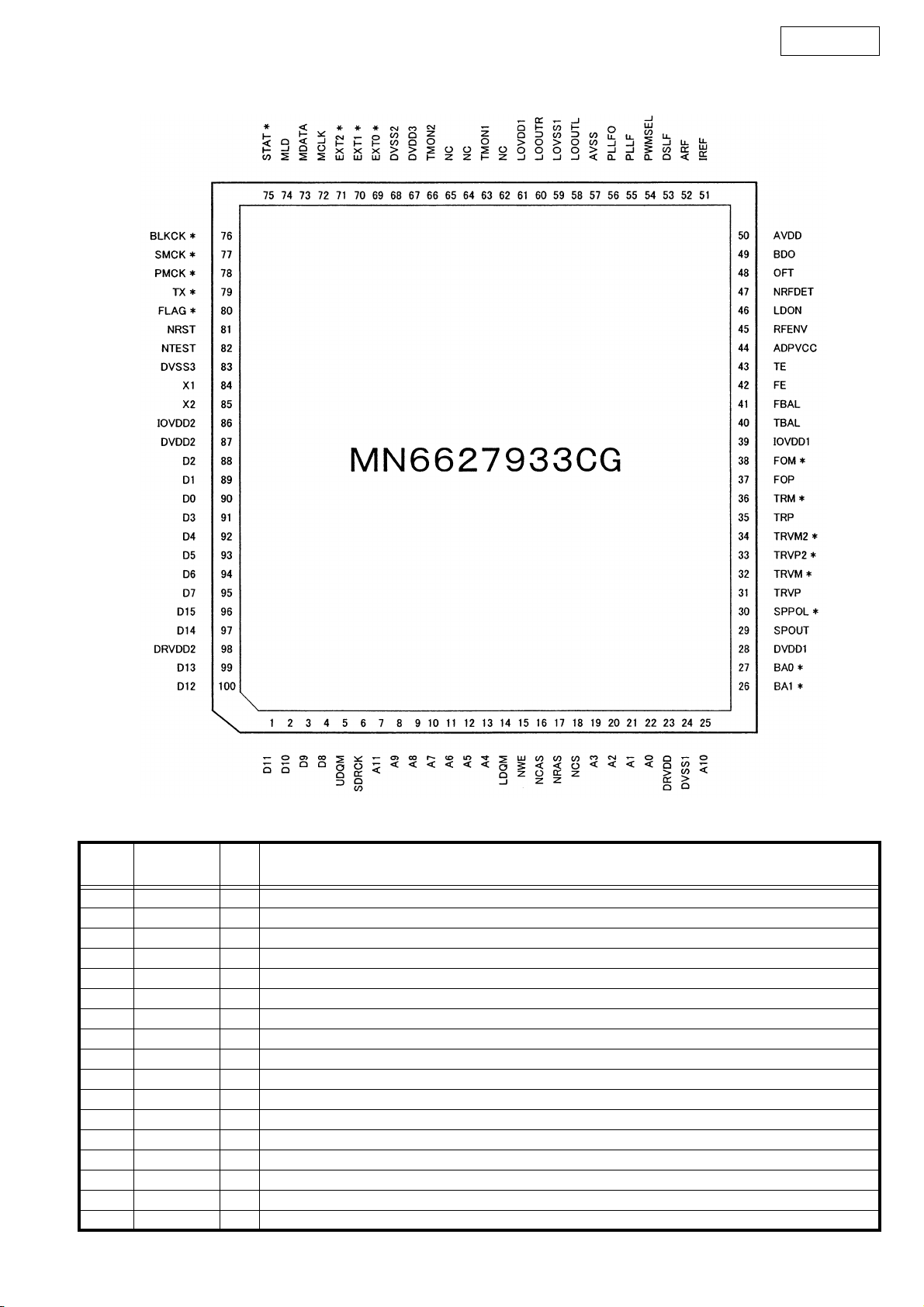
69 *EXT0 I/O Expansion I/O port 0
70 *EXT1 I/O Expansion I/O port 1
71 *EXT2 I/O Expansion I/O port 2
72 MCLK I µcom command clock signal input
19
Page 20

DN-S3500
Pin
No.
100 D12 I/O SDRAM data signal I/O 12
Pin Name I/O Function
73 MDATA I µcom command data signal input
74 MLD I µcom command load signal input
75 *STAT O Status signal output
76 *BLKCK O Subcode block clock signal output
77 *SMCK O 4.2336MHz/8.4672MHz clock signal output
78 *PMCK O 88.2kHz clock signal output
79 *TX O Digital audio interface signal output
80 *FLAG O Flag signal output
81 NRST I LSI reset signal input
82 NTEST I Test mode setup input
83 DVSS3 I GND 3 for digital circuits
84 X1 I Crystal oscillator circuit input
85 X2 O Crystal oscillator circuit output
86 IOVDD2 I Power supply 2 for digital I/O
87 DVDD2 I Power supply 2 for inside digital circuits
88 D2 I/O SDRAM data signal I/O 2
89 D1 I/O SDRAM data signal I/O 1
90 D0 I/O SDRAM data signal I/O 0
91 D3 I/O SDRAM data signal I/O 3
92 D4 I/O SDRAM data signal I/O 4
93 D5 I/O SDRAM data signal I/O 5
94 D6 I/O SDRAM data signal I/O 6
95 D7 I/O SDRAM data signal I/O 7
96 D15 I/O SDRAM data signal I/O 15
97 D14 I/O SDRAM data signal I/O 14
98 DRVDD2 I Power supply 2 for SDRAM interface I/O
99 D13 I/O SDRAM data signal I/O 13
Note) Pins marked with an asterisk can be switched to different signals by using microcontroller commands.
20
Page 21

AN8785SB (IC202)
DN-S3500
1
7
8
14 15
AN22002A (IC203)
L: All mute
Hiz: ch2,4 ON
H: Active
28
22
21
Standby
16
Standby
Band-gap
Vcc/Vref
Reser Circuit
1.25V
+
-
7
IN2+
0.1µ
PVcc2
(2.5V)
10
[ Loading ]
D2+
D2-
M
12 11
-
+
-
+
9
ch.4 SW
H:2.5V
Lor
IN2-
HIZ
-
+
8
[ Traverse ]
D4-
18
-+-
:Vref
IN4
21
-
D4+
17
+
switch
+
15
PGnd2
[ Others ]
[ Spindle ]
D3-
MM
14
-+-
-
+
20
IN3
D3+
13
[ Focus ]
PVcc3
D1-
1
19
+
-+-+-
23 27
IN1
[ Tracking ]
D5-
D5+
IN5
PVcc1
25
24
Protection
Circuit
4
IN-
-
+
-
+
22
2
SVcc
+
-
SGnd-Fin
5
IN+
3
OUT
6
Vref
D1+
26
28
+
-
+
PGnd1
CAGC
RFN
1
16
32
A
+
C
-
+
A
B
+
17
D
-
+
F
-
+
E
-
+
32
C
31
B
30
D
29
27
E
F
28
VREF
17
5
4
RFOUT
RF_EQ
AMP GCA BCA
AMP GCA BCA
AMP
AMP
+
-
6
RFIN
NRFDET
GCA
GCA
7
CBD0
ARF
11
8
AGC BD0 0FTR
BCA
BCA
BD0
12
SUB
SUB
C0FTR
13
3TENV
VDET
+
-
+
-
+
-
0FTR
14
LD
9
10
15
22
23
21
20
19
18
2
CEA
NRFDET
FEN
FEOUT
TEN
TEOUT
TEBPF
VDET
3TOUT
21
PD
1
TBAL
GCTL
24
26
FBAL
25
3
16
VCCGND
Page 22

PCM1748 (IC106)
DN-S3500
BCK
DATA
LRCK
DGND
V
OUT
V
OUT
BCK
LRCK
DATA
ML
1
2
3
4
5
V
DD
6
V
CC
7
L
8
R
PCM1748
Serial
Input
I/F
16
SCK
15
ML
14
MC
13
MD
12
ZEROL/NA
11
ZEROR/ZEROA
10
V
COM
9
AGND
8x
Oversampling
Digital Filter
with
Function
Controller
Enhanced
Multi-Level
Delta-Sigma
Modulator
DAC
Output Amp and
Low-Pass Filter
V
L
OUT
V
COM
Function
MC
MD
SCK
Control
I/F
System Clock
Manager
GP1A038RBK (IC915,916)
1
2
3
6
System Clock
ZEROL
Zero Detect
ZEROR
DAC
Output Amp and
Low-Pass Filter
Power Supply
DD
V
DGND
CC
V
AGND
V
R
OUT
54
22
Page 23

64M SDRAM (IC210)
128M SDRAM (IC402)
154
TOP VIEW
27 28
DN-S3500
Pin Assignment
22, 23~26, A0~A11 Address Multiplexed pins for row and column address.
29~35 Row address: A0~A11. Column address: A0~A8.
20, 21 BS0, Bank Select Select bank to activate during row address latch time, or bank to
2, 4, 5, 7, 8, DQ0~ Data Input/Output Multiplexed pins for data output and input.
10,11, 13, 42, DQ15
44,45, 47, 48,
50, 51, 53
19 CS# Chip Select Disable or enable the command decoder. When command decoder is
18 RAS# Row Address Strobe Command input. When sampled at the rising edge of the clock,
17 CAS#
16 WE# Write Enable Referred to RAS#
15, 39 UDQM/ input/output mask The output buffer is placed at Hi-A (with latency of 2) when DQM is
38 CLK Clock Inputs System clock used to sample inputs on the rising edge of clock.
37 CKE Clock Enable CKE controls the clock activation and deactivation. When CKE is low,
1, 14, 27 Vcc Power (+3.3V) Power for input buffers and logic circuit inside DRAM.
28, 41, 54 Vss Ground Ground for input buffers and logic circuit inside DRAM.
3, 9, 43, 49 VccQ
6, 12, 46, 52 VssQ Ground for I/O buffer Separated ground from Vss, used for output buffers to improve noise.
36, 40 NC No Connection No Connection
Pin Name
BS1 read/write during address latch time.
LDQM sampled high in read cycle. In write cycle, sampling DQM high will
Function
Column Address Strobe
Power (+3.3V) for I/O buffer
disabled, new command is ignored and previous operation continues.
RAS#, CAS# and WE# define the operation to be executed.
Referred to RAS#
block the write operation with zero latency.
Power Down mode, Suspend mode, or Self Refresh mode is entered.
Separated power from Vcc, used for output buffers to improve noise.
DescriptionPin No.
BU2090F (IC602,632,662) TPC6103 (IC410) TOP247YN (IC901)
654
Control Circuit
12-Bit Shift Register
Latch
Output Buffer
(Open Drain)
7Q3
8Q4
16 VDD1Vss
15 Q112DATA
14 Q103CLOCK
13 Q94Q0
12 Q85Q1
11 Q76Q2
10 Q6
Q5
9
123
1C2L3X4S5F7
D
NJM2626 (IC708) EW-510 (IC751-753)
FR
Vref
H1
H2
H3
1
2
3
4
5
16
15
14
13
12
VCC
UH
VH
WH
UL
1 Vcc
REG.
3 Output
OSC
Verr
GND
6
7
8
11
10
VL
Vcc
123
Gnd
Output
WL
9
llimit
2 Gnd
23
Page 24

2. FL DISPLAY 16-MT-82GINK (FL601)
144
Pin Connection
DN-S3500
24
Page 25

PRINTED WIRING BOARDS
GU-3689 MAIN P.W.B. UNIT
DN-S3500
25
COMPONENT SIDE
Page 26

DN-S3500
26
FOIL SIDE
Page 27

GU-3690 POWER P.W.B. UNIT
DN-S3500
27
COMPONENT SIDE
Page 28

DN-S3500
28
FOIL SIDE
Page 29

GU-3691 PANEL P.W.B. UNIT
DN-S3500
29
COMPONENT SIDE
Page 30

DN-S3500
30
FOIL SIDE
Page 31

GU-3717 PANEL P.W.B. UNIT
DN-S3500
COMPONENT SIDE FOIL SIDE
31
Page 32

DN-S3500
NOTE FOR PARTS LIST
• Part indicated with the mark "nsp" are not always in stock and possibly to
take a long period of time for supplying, or in some case supplying of part
may be refused.
• When ordering of part, clearly indicate "1" and "I" (i) to avoid mis-
supplying.
• Ordering part without stating its part number can not be supplied.
• Part indicated with the mark " ★ " is not illustrated in the exploded view.
• Not including Carbon Film Resister ±5%, 1/4W Type in the P.W.Board
parts list. (Refer to the Schematic Diagram for those parts.)
• Not including Carbon Chip Resister 1/16W Type in the P.W.Board parts
list. (Refer to the Schematic Diagram for those parts.)
WARNING:
Parts marked with this symbol ! have critical characteristics.
Use ONLY replacement parts recommended by the manufacturer.
ll
Resistors
l
ll
Ex.: RN 14K 2E 182 G FR
Type Shape Power Resist- Allowable Others
and per- ance error
formance
RD : Carbon 2B : 1/8W F : ±1% P : Pulse-resistant type
RC : Composition 2E : 1/4W G : ±2% NL : Low noise type
RS : Metal oxide film 2H : 1/2W J : ±5% NB : Non-burning type
RW : Winding 3A : 1W K : ±10% FR : Fuse-resistor
RN : Metal film 3D : 2W M : ±20% F : Lead wire forming
RK : Metal mixture 3F : 3W
] Resistance
1 8 2 ⇒ 1800 ohm = 1.8 kohm
s
s
• Units: ohm
1 R 2 ⇒ 1.2 ohm
s
s
• Units: ohm
3H : 5W
Indicates number of zeros after effective number.
2-digit effective number.
1-digit effective number.
2-digit effective number, decimal point indicated by R.
部品表について
1.nsp 印の部品は常時在庫していませんので供給に長時間を要すること
があります。
場合によっては、供給をお断りすることがあります。
2.部品を発注する際は特に数字の " 1 " と英字の "I" との区別をはっき
り記入してください。
3.部品番号を表示していない部品は供給できません。
4.!印の部品は安全上重要な部品です。交換するときは、安全および性
能維持のため必ず指定の部品をご使用ください。
5.★印のついている部品は分解図中には記載していません。
6.カーボン抵抗器± 5%、1/4W 型は記載していません。定数は回路図を
参照願います。
7.カーボンチップ抵抗器 1/16W 型は記載していません。定数は回路図を
参照願います。
8.部品表の抵抗器、コンデンサの品名記号の読み方は表を参照してくだ
さい。
RN 14K 2E 182 G FR
RD : 2B : 1/8 W F : ±1% P :
RC : 2E : 1/4 W G : ±2% NL :
RS : 2H : 1/2 W J : ±5% NB :
RW : 3A : 1 W K : ±10% FR :
RN : 3D : 2 W M : ±20% F :
RK : 3F : 3 W
∗
18 2
1R 2
3H : 5 W
1800
Ö
2
1.2
Ö
1
2 R
=1.8k
0
ll
l Capacitors
ll
Ex.: CE 04W 1H 2R2 M BP
Type Shape Dielectric Capacity Allowable Others
and per- strength error
formance
CE : Aluminum foil 0J : 6.3V F : ±1% HS : High stability type
electrolytic
CA : Aluminum solid 1A : 10V G : ±2% BP : Non-polar type
electrolytic
CS : Tantalum electrolytic 1C : 16V J : ±5% HR : Ripple-resistant type
CQ : Film 1E : 25V K : ±10% DL : For change and discharge
CK : Ceramic 1V : 35V M : ±20% HF : For assuring high
CC : Ceramic 1H : 50V Z : +80% U : UL par t
CP : Oil 2A : 100V –20% C : CSA part
CM : Mica 2B : 125V P : +100% W : UL-CSA type
CF : Metallized 2C : 160V –0% F : Lead wire forming
CH : Metallized 2D : 200V C : ±0.25pF
] Capacity (electrolyte only)
2 2 2 ⇒ 2200µF
s
s
• Units: µF.
2 R 2 ⇒ 2.2µF
s
s
• Units: µF.
] Capacity (except electrolyte)
2 2 2 ⇒ 2200pF=0.0022µF
s
s
(More than 2) Indicates number of zeros after effective number.
• Units: pF.
2 2 1 ⇒ 220pF
s
s
(0 or 1) Indicates number of zeros after effective number.
• Units: pF.
• When the dielectric strength is indicated in AC, "AC" is included after the dieelectric
strength value.
2E : 250V D : ±0.5pF
2H : 500V = : Others
2J : 630V
Indicates number of zeros after effective number.
2-digit effective number.
1-digit effective number.
2-digit effective number, decimal point indicated by R.
2-digit effective number.
2-digit effective number.
requency
CE 04W 1H 2R2 M BP
CE : 0J : 6.3 V F : ±1% HS :
CA : 1A : 10 V G : ±2% BP :
CS : 1C : 16 V J : ±5% HR :
CQ : 1E : 25 V K : ±10% DL :
CK : 1V : 35 V M : ±20% HF :
CC : 1H : 50 V Z : +80% U : UL
CP : 2A : 100 V −20% C : CSA
CM : 2B : 125 V P : +100% W : UL-CSA
CF : 2C : 160 V − 0% F :
CH : 2D : 200 V C : ±0.25pF
2E : 250 V D : ±0.5pF
2H : 500 V = :
2J : 630 V
∗
22 2
22 2
2200µF
Ö
2
µ
F
2200pF=0.0022µF
Ö
(0 2 )
2
p
F
0
0
2R 2
22 1
Ö
1
2 R
µ
F
Ö
(0 0 1 )
2
p
F
AC
2.2µF
220pF
0
32
Page 33

DN-S3500
PARTS LIST OF P.W.B. UNIT
*本表に記載されている部品は、補修用部品のため製品に使用している部品とは一部、形状、寸法などが異なる場合があります。
* The parts listed below are for maintenance only, might differ from the parts used in the unit in appearances or dimensions.
*"nsp" 印の部品は常時在庫していませんので供給に長時間を要することがあります。場合によっては、供給をお断りする場合があります。
* Part indicated with the mark “nsp” are not always in stock and possibly to take a long period of time for supplying, or in some case supplying of part may be refused.
Note: The symbols in the column "Remarks" indicate the following destinations.
E3: U.S.A. & Canada model E2: Europe model
JP: Japan model
GU-3689 MAIN P.W.B. UNIT ASS'Y
Ref. No. nsp Part No. Part Name Remarks Q'ty New
SEMICONDUCTORS GROUP
IC101 00D 262 3044 001 MN102H730F
IC102 00D GEN 8017 SYSTEM ROM SUB ASSY 8M FLASH MEMORY(70N)
IC103 00D 262 3082 911 BD4745G
IC104 00D 262 1953 903 TC7WU04F +C
IC105 00D 262 3305 902 SN74LV393APW
IC106 00D 262 3166 905 PCM1748E(TAPE) +C
IC107 00D 262 2640 901 SN74LV245APW-EL2
IC108 00D 262 3305 902 SN74LV393APW
IC109 00D 262 2517 908 SN74LV08APW-EL2 +REF
IC110 00D 263 1079 903 BA033FP +C
IC111 00D 262 3513 008 8M FLASH MEMORY(90N)
IC113 00D 262 2948 904 SN74LV86APW +REF
IC201 00D 262 3398 003 MN6627933
IC202 00D 262 3159 909 AN8785SB
IC203 00D 262 3160 901 AN22002A
IC207 00D 263 0615 902 BA15218F-DXE2 +C
IC210 00D 262 3401 000 64M SDRAM(TSOP)
IC401 00D 262 3399 002 ADSP-BF531(LQFP)
IC402 00D 262 3407 004 128M SDRAM(TSOP)PBF
IC403,404 00D 262 2640 901 SN74LV245APW-EL2
IC405 00D 262 2959 906 SN74LV244APW +REF
IC406 00D 262 2640 901 SN74LV245APW-EL2
IC408 00D 262 2518 907 SN74LV74APW-EL2 +C
IC409 00D 262 2516 909 SN74LV32APW-EL2 +C
IC410 00D 262 3400 904 TPC6103
TR201 00D 272 0125 904 2SB709A +C
TR202,203 00D 269 0082 902 DTC114EKT96 +C
TR301 00D 269 0082 902 DTC114EKT96 +C
TR302 00D 269 0083 901 DTA114EKT96 +C
TR303 00D 273 0437 909 2SC2411K-T146 +C
TR304 00D 271 0260 905 2SA1036KT146(S/R) +C
D101 00D 276 0559 909 DAP202KT146 +C
D401 00D 276 0559 909 DAP202KT146 +C
D402 00D 276 0750 902 RB521S-30TE61 +REF
CAPACITORS GROUP
C101 nsp 00D 257 0512 903 CK73F1E104ZT +1608
C102 00D 257 4011 905 CE67C0J101MT (RV2) +REF
C104-107 nsp 00D 257 0512 903 CK73F1E104ZT +1608
C108 00D 257 4011 905 CE67C0J101MT (RV2) +REF
C109 nsp 00D 257 0506 951 CC73CH1H101JT +1608
C110-113 nsp 00D 257 0512 903 CK73F1E104ZT +1608
C114 nsp 00D 257 0506 951 CC73CH1H101JT +1608
33
Page 34

DN-S3500
Ref. No. nsp Part No. Part Name Remarks Q'ty New
C115 nsp 00D 257 0509 929 CK73B1H102KT +1608
C116 nsp 00D 257 0512 903 CK73F1E104ZT +1608
C117 00D 257 4011 905 CE67C0J101MT (RV2) +REF
C118,119 nsp 00D 257 0512 903 CK73F1E104ZT +1608
C120 nsp 00D 257 0503 967 CC73CH1H150JT +1608
C121 nsp 00D 257 0511 904 CK73F1H103ZT +1608
C122 nsp 00D 257 0512 903 CK73F1E104ZT +1608
C123 nsp 00D 257 0509 929 CK73B1H102KT +1608
C124 nsp 00D 257 0506 951 CC73CH1H101JT +1608
C125 nsp 00D 257 0503 967 CC73CH1H150JT +1608
C126 nsp 00D 257 0516 954 CK73B1E104KT +1608
C127 00D 257 4011 905 CE67C0J101MT (RV2) +REF
C128 nsp 00D 257 0511 904 CK73F1H103ZT +1608
C129 00D 257 4011 905 CE67C0J101MT (RV2) +REF
C130,131 nsp 00D 257 0516 954 CK73B1E104KT +1608
C132 00D 257 4012 904 CE67C1C100MT (RV2B55 +REF
C133 00D 257 4011 905 CE67C0J101MT (RV2) +REF
C134,135 nsp 00D 257 0512 903 CK73F1E104ZT +1608
C136 00D 257 4012 933 CE67C1C101MT (RV2) +REF
C137,138 nsp 00D 257 0504 940 CC73CH1H330JT +1608
C148-152 nsp 00D 257 0509 929 CK73B1H102KT +1608
C153,154 nsp 00D 257 0512 903 CK73F1E104ZT +1608
C155 nsp 00D 257 0509 929 CK73B1H102KT +1608
C156 nsp 00D 257 0516 954 CK73B1E104KT +1608
C157 nsp 00D 257 0511 904 CK73F1H103ZT +1608
C158 nsp 00D 257 0512 903 CK73F1E104ZT +1608
C159 nsp 00D 257 0516 954 CK73B1E104KT +1608
C201 nsp 00D 257 0512 903 CK73F1E104ZT +1608
C202 nsp 00D 257 0509 929 CK73B1H102KT +1608
C203 nsp 00D 257 0512 903 CK73F1E104ZT +1608
C204 nsp 00D 257 0509 929 CK73B1H102KT +1608
C205 nsp 00D 257 0516 909 CK73B1E223KT +1608
C206 nsp 00D 257 0512 903 CK73F1E104ZT +1608
C208 00D 254 4655 922 CE67C0J470MT (RV2) +REF
C211,212 nsp 00D 257 0512 903 CK73F1E104ZT +1608
C213 nsp 00D 257 0509 929 CK73B1H102KT +1608
C214 nsp 00D 257 0512 903 CK73F1E104ZT +1608
C216 nsp 00D 257 0510 950 CK73B1H682KT +1608
C217-220 nsp 00D 257 0509 990 CK73B1H222KT +1608
C222,223 nsp 00D 257 0516 909 CK73B1E223KT +1608
C224 nsp 00D 257 0512 903 CK73F1E104ZT +1608
C227 nsp 00D 257 0512 903 CK73F1E104ZT +1608
C228 00D 257 4011 905 CE67C0J101MT (RV2) +REF
C229 nsp 00D 257 0504 937 CC73CH1H300JT +1608
C231,232 00D 254 4655 922 CE67C0J470MT (RV2) +REF
C233 00D 257 4011 905 CE67C0J101MT (RV2) +REF
C234 nsp 00D 257 0512 903 CK73F1E104ZT +1608
C237 nsp 00D 257 0512 903 CK73F1E104ZT +1608
C238 nsp 00D 257 0501 914 CK73B1H123KT +1608
C239 nsp 00D 257 0510 947 CK73B1H562KT +1608
C240 nsp 00D 257 0516 909 CK73B1E223KT +1608
C241 nsp 00D 257 0501 927 CK73B1H153KT +1608
C242 nsp 00D 257 0506 919 CC73CH1H680JT +1608
C243 nsp 00D 257 0512 903 CK73F1E104ZT +1608
C244 00D 257 4011 905 CE67C0J101MT (RV2) +REF
C245 nsp 00D 257 0507 950 CC73CH1H271JT +1608
34
Page 35

DN-S3500
Ref. No. nsp Part No. Part Name Remarks Q'ty New
C246 nsp 00D 257 0506 993 CC73CH1H151JT +1608
C250 nsp 00D 257 0512 903 CK73F1E104ZT +1608
C251 00D 254 4661 929 CE67C1H4R7MT (RV2) +REF
C252 00D 257 4011 905 CE67C0J101MT (RV2) +REF
C253 nsp 00D 257 0512 903 CK73F1E104ZT +1608
C254 00D 257 4011 905 CE67C0J101MT (RV2) +REF
C255 nsp 00D 257 0520 911 CK73B1A224KT +1608
C256 nsp 00D 257 0520 908 CK73B1A154KT +1608
C257 00D 257 4011 905 CE67C0J101MT (RV2) +REF
C261,262 00D 257 4012 904 CE67C1C100MT (RV2B55 +REF
C263,264 nsp 00D 257 0510 918 CK73B1H332KT +1608
C265,266 nsp 00D 257 0506 935 CC73CH1H820JT +1608
C267,268 nsp 00D 257 0512 903 CK73F1E104ZT +1608
C274 nsp 00D 257 0512 903 CK73F1E104ZT +1608
C280 00D 257 4011 905 CE67C0J101MT (RV2) +REF
C281 nsp 00D 257 0512 903 CK73F1E104ZT +1608
C282 00D 254 4658 916 CE67C1E100MT (RV2)
C283-285 nsp 00D 257 0512 903 CK73F1E104ZT +1608
C291,292 nsp 00D 257 0512 903 CK73F1E104ZT +1608
C293 00D 257 4012 933 CE67C1C101MT (RV2) +REF
C295 nsp 00D 257 0512 903 CK73F1E104ZT +1608
C298 nsp 00D 257 0512 903 CK73F1E104ZT +1608
C301 nsp 00D 257 0512 903 CK73F1E104ZT +1608
C302,303 00D 254 4660 946 CE67C1H010MT (RV2B55 +REF
C304,305 nsp 00D 257 0509 929 CK73B1H102KT +1608
C306 nsp 00D 257 0512 903 CK73F1E104ZT +1608
C307 nsp 00D 257 0509 929 CK73B1H102KT +1608
C401 nsp 00D 257 0509 929 CK73B1H102KT +1608
C402-406 nsp 00D 257 0512 903 CK73F1E104ZT +1608
C407 00D 257 4011 905 CE67C0J101MT (RV2) +REF
C408-412 nsp 00D 257 0512 903 CK73F1E104ZT +1608
C413 nsp 00D 257 0509 929 CK73B1H102KT +1608
C414 00D 257 4011 905 CE67C0J101MT (RV2) +REF
C415-419 nsp 00D 257 0512 903 CK73F1E104ZT +1608
C420 00D 257 4011 905 CE67C0J101MT (RV2) +REF
C421,422 nsp 00D 257 0512 903 CK73F1E104ZT +1608
C423 00D 257 4011 905 CE67C0J101MT (RV2) +REF
C424-429 nsp 00D 257 0512 903 CK73F1E104ZT +1608
C431 nsp 00D 257 0512 903 CK73F1E104ZT +1608
C432 nsp 00D 257 0511 904 CK73F1H103ZT +1608
C433-438 nsp 00D 257 0512 903 CK73F1E104ZT +1608
C439 00D 257 4011 905 CE67C0J101MT (RV2) +REF
C440-443 nsp 00D 257 0512 903 CK73F1E104ZT +1608
OTHERS PARTS GROUP
CX061 nsp 00D 205 1072 946 6P PH CON.BASE +REF
CX121 00D 205 1314 934 12P FFC BASE(9616S)Y
CX181 00D 205 1314 947 18P FFC BASE(9616S)Y
CX251 00D 205 1313 906 25P FFC.BASE(9610SCA +REF
CX361 00D 205 1367 907 28P FFC BASE(FMN BT)
FB101 nsp 00D 235 0158 901 CHIP BEADS(18PG121) +1608
FB103-116 nsp 00D 235 0130 903 CHIP EMIFIL(11A121) +1608
FB118,119 nsp 00D 235 0130 903 CHIP EMIFIL(11A121) +1608
FB201-204 nsp 00D 235 0106 908 CHIP EMIFIL (21A05) +C
35
Page 36

DN-S3500
Ref. No. nsp Part No. Part Name Remarks Q'ty New
FB401 nsp 00D 235 0158 901 CHIP BEADS(18PG121) +1608
X101 00D 399 1029 906 CSACW32M0X51-R0
X102 00D 399 1031 907 XTAL(11.2896M/SMT)
X201 00D 399 0978 906 CSTCG25M0V53-R0
X401 00D 399 0978 906 CSTCG25M0V53-R0
-RADIATOR
36
Page 37

GU-3690/36902 POWER P.W.B. UNIT ASS'Y
Ref. No. nsp Part No. Part Name Remarks Q'ty New
SEMICONDUCTORS GROUP
IC701 00D 262 3531 909 SN74HCT14PW
IC702 00D 262 1346 905 TC74HC08AF(TP1) +C
IC703,704 00D 263 0845 905 NJM3404AM-TE1
IC705 00D 262 1875 900 BU4066BCF-T1 +C
IC706 00D 263 0845 905 NJM3404AM-TE1
IC707 00D 262 3530 900 TC74HC86AF
IC708 00D 262 3532 908 NJM2626
IC802 00D 262 1953 903 TC7WU04F +C
IC901 00D 265 0126 002 TOP247YN
IC902 00D 262 3047 008 PC123Y22
IC903 00D 263 0809 006 NJM7805FA(S)
IC913 00D 263 0810 008 NJM7808FA(S)
IC914 00D 263 1206 912 TA76432F
TR701,702 00D 269 0082 902 DTC114EKT96 +C
TR703 00D 275 0113 902 2SJ377(SMT)
TR704 00D 275 0114 901 2SK2231(SMT)
TR705 00D 275 0113 902 2SJ377(SMT)
TR706 00D 275 0114 901 2SK2231(SMT)
TR707 00D 275 0113 902 2SJ377(SMT)
TR708 00D 275 0114 901 2SK2231(SMT)
TR709-712 00D 269 0082 902 DTC114EKT96 +C
TR805 00D 273 0460 905 KTC2875B-RTK +C
TR806 00D 273 0426 907 2SC2412KLNT146 +C
TR807,808 00D 273 0460 905 KTC2875B-RTK +C
TR809 00D 269 0082 902 DTC114EKT96 +C
TR810 00D 269 0083 901 DTA114EKT96 +C
TR811-813 00D 269 0082 902 DTC114EKT96 +C
TR901 00D 271 0308 906 2SA933ASTPS
TR902 00D 274 0158 016 2SD1763A(E)
DN-S3500
D701 00D 276 0787 001 RN2Z
D803 00D 276 0559 909 DAP202KT146 +C
D804 00D 276 0560 901 DAN202KT146 +C
D805 00D 276 0717 903 1SS355 TE-17 +C
D806 00D 276 0559 909 DAP202KT146 +C
D807 00D 276 0560 901 DAN202KT146 +C
D901-904 00D 276 0729 904 EM01AT (V1)
D905,906 00D 276 0813 001 AP01C
D908 00D 276 0401 905 1SS133T77 (TAPE)
D909 00D 276 0757 002 FML-G12S
D910 00D 276 0832 008 FMX-G22S
D912-914 00D 276 0730 906 AG01ZT (V1)
ZD902 00D 276 0762 945 MTZJ36B T77
ZD903 00D 276 0831 902 0ZDZ2.4-Z
TH901 00D 279 0044 002 NTH11D8R0LA
RESISTORS GROUP
R744 00D 244 2043 982 RS14B3AR22JNBST(S)
R901 00D 244 2675 729 RS14B3D224JNBF (ERG)
VR701 00D 211 6132 983 V06PB104T
37
Page 38

Ref. No. nsp Part No. Part Name Remarks Q'ty New
CAPACITORS GROUP
C701 nsp 00D 257 0508 917 CC73CH1H471JT +1608
C702 nsp 00D 257 0506 951 CC73CH1H101JT +1608
C703 nsp 00D 257 0508 917 CC73CH1H471JT +1608
C704 nsp 00D 257 0516 954 CK73B1E104KT +1608
C705 nsp 00D 257 0516 941 CK73B1E473KT +1608
C706 nsp 00D 257 0512 903 CK73F1E104ZT +1608
C707 nsp 00D 257 0516 941 CK73B1E473KT +1608
C708 nsp 00D 257 0501 901 CK73B1H103KT (1608) +1608
C709 nsp 00D 257 0520 911 CK73B1A224KT +1608
C710,711 nsp 00D 257 0512 903 CK73F1E104ZT +1608
C712 nsp 00D 257 0511 904 CK73F1H103ZT +1608
C713 nsp 00D 257 0501 901 CK73B1H103KT (1608) +1608
C714 00D 254 4524 943 CE04W1H010MT SMG/RE3
C715 nsp 00D 257 0509 990 CK73B1H222KT +1608
C716 00D 254 4522 783 CE04W1V471MC SMG/RE3
C717 nsp 00D 257 0512 903 CK73F1E104ZT +1608
C718-721 nsp 00D 257 0501 901 CK73B1H103KT (1608) +1608
C722-725 nsp 00D 257 0512 903 CK73F1E104ZT +1608
C726 00D 254 4524 943 CE04W1H010MT SMG/RE3
C727 00D 254 4528 729 CE04W2A101MC SMG/RE3
C728,729 nsp 00D 257 0516 954 CK73B1E104KT +1608
C730 00D 254 4524 972 CE04W1H4R7MT SMG/RE3
C819 nsp 00D 257 0509 929 CK73B1H102KT +1608
C820 nsp 00D 257 0501 901 CK73B1H103KT (1608) +1608
C821 nsp 00D 257 0512 903 CK73F1E104ZT +1608
C822 00D 254 4536 928 CE04W1A101MT SMG/RE3
C824 00D 254 4524 943 CE04W1H010MT SMG/RE3
C825,826 00D 254 4538 900 CE04W1C100MT SMG/RE3
C827,828 nsp 00D 257 0509 929 CK73B1H102KT +1608
C829,830 nsp 00D 257 0512 903 CK73F1E104ZT +1608
C831 nsp 00D 257 0508 917 CC73CH1H471JT +1608
C832 nsp 00D 257 0511 904 CK73F1H103ZT +1608
C833 nsp 00D 257 0508 917 CC73CH1H471JT +1608
C834 nsp 00D 257 0511 904 CK73F1H103ZT +1608
C835 nsp 00D 257 0508 917 CC73CH1H471JT +1608
C836 nsp 00D 257 0511 904 CK73F1H103ZT +1608
C838 nsp 00D 257 0508 917 CC73CH1H471JT +1608
C839,840 nsp 00D 257 0507 934 CC73CH1H221JT +1608
C841 nsp 00D 257 0508 917 CC73CH1H471JT +1608
C842,843 nsp 00D 257 0507 934 CC73CH1H221JT +1608
! C901 00D 253 8022 707 CK45F2EAC103MC
C902 00D 256 8038 004 CF99--2EAC104M
C903 00D 253 8029 713 CK45F2EAC471KC(KX)
C904 00D 254 4588 714 CE04W2D221MC(KMG) for E3, JP
C904 00D 254 4589 713 CE04W2G101MC(KMG) for E2
C905,906 00D 253 8029 713 CK45F2EAC471KC(KX)
C907 00D 257 3013 933 CF73=1H104JT(ECHUC9) +C
C909 00D 256 8038 004 CF99--2EAC104M
C910 00D 254 4525 913 CE04W1H470MT SMG/RE3
C911 00D 253 8029 713 CK45F2EAC471KC(KX)
C912 00D 257 3013 933 CF73=1H104JT(ECHUC9) +C
C913 00D 254 4525 913 CE04W1H470MT SMG/RE3
C914 00D 254 4756 902 CE04W1H101MT HB5(KY) for E3, JP
C914 00D 254 4708 905 CE04W1E221MT HB5(KY) for E2
C915 00D 254 4756 902 CE04W1H101MT HB5(KY)
DN-S3500
2
2
38
Page 39

DN-S3500
Ref. No. nsp Part No. Part Name Remarks Q'ty New
C916 00D 253 8029 713 CK45F2EAC471KC(KX)
C918 00D 254 4710 906 CE04W1C331MT HB5(KY)
C919 00D 254 4758 706 CE04W1V272MCL35(KY)
C923 00D 254 4525 913 CE04W1H470MT SMG/RE3
C925,926 00D 254 4757 707 CE04W1E272MCL25(KY)
C927 00D 254 4541 942 CE04W1E101MT SMG/RE3
C931 nsp 00D 257 0512 903 CK73F1E104ZT +1608
C934,935 nsp 00D 257 0512 903 CK73F1E104ZT +1608
C937 00D 254 4538 939 CE04W1C470MT SMG/RE3
C940,941 nsp 00D 257 0512 903 CK73F1E104ZT +1608
C942 00D 254 4541 942 CE04W1E101MT SMG/RE3
C943 00D 254 4525 913 CE04W1H470MT SMG/RE3
C944 00D 254 4541 942 CE04W1E101MT SMG/RE3
C945,946 nsp 00D 257 0512 903 CK73F1E104ZT +1608
C948-950 nsp 00D 257 0512 903 CK73F1E104ZT +1608
C951 00D 254 4756 902 CE04W1H101MT HB5(KY) for E3, JP
C951 00D 254 4708 905 CE04W1E221MT HB5(KY) for E2
2
OTHERS PARTS GROUP
CW121 nsp 00D 205 0375 026 12P CONN.BASE(KR-PH)
CX021 nsp 00D 205 0581 001 2P VH CONNECTOR BASE
CY061 nsp 00D 204 0579 023 6P PH-SAN CON.CORD
CY361 00D 205 1100 041 28P FFC BASE (P=1)
! F901 00D 206 1089 000 FUSE (ET0.8A) for E3, JP
! F901 00D 206 1089 013 FUSE(ET1.25A) for E2
FB801,802 nsp 00D 235 0130 903 CHIP EMIFIL(11A121) +1608
FF901 nsp 00D 202 0040 909 FUSE CLIP(TAPE)
FH901 nsp 00D 202 0040 909 FUSE CLIP(TAPE)
JK802 00D 204 8664 011 3P PIN JACK
JK804-806 00D 204 8416 007 MINI JACK
L901 00D 235 0157 009 PLA10AN7720R7D2B
L907 00D 235 0159 007 PLH10AN3711ROP2B
! S901 00D 212 1176 015 POWER SWITCH(TV-5)
2
! T901 00D 233 0699 008 SW TRANSFORMER
-RADIATOR
nsp 00D 471 3304 015 3X8 CBS-Z
nsp 00D GEN 8038 FUSE LABEL SUB ASSY for F901, for E2
39
Page 40

GU-3691 PANEL P.W.B. UNIT ASS'Y
Ref. No. nsp Part No. Part Name Remarks Q'ty New
SEMICONDUCTORS GROUP
IC602 00D 262 2745 903 BU2090F(E2) +C
IC603 00D 262 2514 901 SN74LV138APW-EL2 +C
IC632 00D 262 2745 903 BU2090F(E2) +C
IC633 00D 262 2514 901 SN74LV138APW-EL2 +C
IC662 00D 262 2745 903 BU2090F(E2) +C
TR601-605 00D 269 0083 901 DTA114EKT96 +C
TR606 00D 271 0260 905 2SA1036KT146(S/R) +C
TR607 00D 269 0082 902 DTC114EKT96 +C
TR608 00D 271 0260 905 2SA1036KT146(S/R) +C
TR609 00D 269 0082 902 DTC114EKT96 +C
TR610 00D 271 0260 905 2SA1036KT146(S/R) +C
TR611 00D 269 0082 902 DTC114EKT96 +C
D604 00D 276 0559 909 DAP202KT146 +C
D606 00D 276 0559 909 DAP202KT146 +C
D608 00D 276 0559 909 DAP202KT146 +C
D611-613 00D 276 0559 909 DAP202KT146 +C
D631-636 00D 276 0559 909 DAP202KT146 +C
D638 00D 276 0559 909 DAP202KT146 +C
D641-643 00D 276 0559 909 DAP202KT146 +C
DN-S3500
LD601-604 00D 393 9606 909 SEL6927A(TP5)
LD605 00D 393 9608 907 SLR342MC(TB7)
LD606,607 00D 393 9606 909 SEL6927A(TP5)
LD608,609 00D 393 9659 901 SELU5E23C-P(BLU)
LD610 00D 393 9612 906 SELU5E20C(TP15)
LD611,612 00D 393 9661 009 SELS1E10CXM-M
LD613 00D 393 9633 008 SELU1250CM(RED)
LD614 00D 393 9660 903 SELU5223C-S(RED)
LD615 00D 393 9633 008 SELU1250CM(RED)
LD616,617 00D 393 9604 901 SEL6227S(TP5)
LD618 00D 393 9607 908 SLR342VC(TB7)
LD619 00D 393 9608 907 SLR342MC(TB7)
LD620,621 00D 393 9604 901 SEL6227S(TP5)
LD622-625 00D 393 9605 900 SEL6427EP(TP5)
LD631,632 00D 393 9605 900 SEL6427EP(TP5)
LD633 00D 393 9607 908 SLR342VC(TB7)
LD634 00D 393 9608 907 SLR342MC(TB7)
LD635,636 00D 393 9609 906 SLR342DC(TB7)
LD637 00D 393 9605 900 SEL6427EP(TP5)
LD643 00D 393 9605 900 SEL6427EP(TP5)
LD648 00D 393 9608 907 SLR342MC(TB7)
LD649 00D 393 9609 906 SLR342DC(TB7)
LD661,662 00D 393 9605 900 SEL6427EP(TP5)
LD663,664 00D 393 9606 909 SEL6927A(TP5)
LD665,666 00D 393 9608 907 SLR342MC(TB7)
LD667 00D 393 9605 900 SEL6427EP(TP5)
LD673 00D 393 9605 900 SEL6427EP(TP5)
LD679,680 00D 393 9608 907 SLR342MC(TB7)
FL601 00D 393 8085 000 FLT(16-MT-82GINK)
40
Page 41

Ref. No. nsp Part No. Part Name Remarks Q'ty New
RESISTORS GROUP
VR601 00D 211 5648 119 SLIDE VOLUME (100MM)
CAPACITORS GROUP
C601-606 nsp 00D 257 0512 903 CK73F1E104ZT +1608
C607 00D 254 4300 947 CE04W0J470MT(SRE)
C608,609 nsp 00D 257 0512 903 CK73F1E104ZT +1608
C611-613 nsp 00D 257 0512 903 CK73F1E104ZT +1608
C614 00D 254 4300 963 CE04W0J101MT(SRE)
C615,616 nsp 00D 257 0512 903 CK73F1E104ZT +1608
C617-619 nsp 00D 257 0509 929 CK73B1H102KT +1608
C637 00D 254 4300 947 CE04W0J470MT(SRE)
C638 nsp 00D 257 0512 903 CK73F1E104ZT +1608
C642 nsp 00D 257 0512 903 CK73F1E104ZT +1608
C667 00D 254 4300 947 CE04W0J470MT(SRE)
C668,669 nsp 00D 257 0512 903 CK73F1E104ZT +1608
C671-675 nsp 00D 257 0509 990 CK73B1H222KT +1608
DN-S3500
OTHERS PARTS GROUP
CW031 nsp 00D 203 5280 013 3P KR-DS CONN.CORD
CW032 nsp 00D 203 5280 042 3P KR-DS CONN.CORD
CW041 nsp 00D 203 6393 022 4P KR-DS CON CORD
CW101 nsp 00D 204 3003 004 10P KR-DS CON.CORD
CW131 nsp 00D 204 6805 005 13P KR-DS CON.CORD
CX031,032 nsp 00D 205 0355 033 3P KR CON BASE(L)
CX041 nsp 00D 205 0355 046 4P KR CON BASE(L)
CX101 nsp 00D 205 0480 005 10P KR CON BASE(L)
CX131 nsp 00D 205 0480 034 13P KR CON BASE(L)
CY251 00D 205 1316 000 25P FFC BASE(9610S)Y
S601 00D 212 0495 001 TOGGLE SW(PADORU)
S607-618 00D 212 5604 907 TACT SWITCH-TA(ALPS)
S623 00D 212 0410 002 ROTARY ENCODER-JOG SWITCH
S637-648 00D 212 5604 907 TACT SWITCH-TA(ALPS)
S653 00D 212 0410 002 ROTARY ENCODER-JOG SWITCH
S667-677 00D 212 5604 907 TACT SWITCH-TA(ALPS)
00D 146 2446 007 DJ MARK
nsp 00D 443 1608 103 FL HOLDER
nsp 00D 461 0984 091 FL SPACER
41
Page 42

GU-3717 MOTOR P.W.B. UNIT ASS'Y
Ref. No. nsp Part No. Part Name Remarks Q'ty New
SEMICONDUCTORS GROUP
IC751-753 00D 262 3533 004 EW-510
IC915,916 00D 269 0226 001 GP1A038RBK
CAPACITORS GROUP
C751-755 nsp 00D 257 0512 903 CK73F1E104ZT +1608
OTHERS PARTS GROUP
CW042 nsp 00D 203 6615 014 4P KR-DS CON.CORD
CW141 nsp 00D 203 6615 014 4P KR-DS CON.CORD
CX041,042 nsp 00D 205 0355 046 4P KR CON BASE(L)
CX121 nsp 00D 205 0480 021 12P KR CON BASE(L)
DN-S3500
42
Page 43

EXPLODED VIEW
Parts marked with this symbol have critical
characteristics.
Use ONLY replacement parts recommended by
the manufacturer.
WARNING:
印の部分は安全を維持するために重要
な部品です。従って交換時は必ず指定の
部品を使用してください。
DN-S3500
48
44A
45
68
49
50
44
3-5
61
30
62
26
34
41
29
36
62
43
62
69
17
63
13
9
69
42
36
62
36
35
69
2
16
14
15
A
8
32
18
36
33
3-3
64
71
10
60
11
66
71
C
6
69
5
40
1
46
47
74
67
C
38
68
37
71
21
23
F
12
73
72
66
69
19
B
65
6
D
69
7
20
69
D
7
D
66
E
24
3-4
D
3-6
23
22
25
4
A
B
F
69
27
31
3-1
28
6
63
69
64
69
66
E
7
39
6
69
7
70
66
66
3-2
66
66
71
43
Page 44

DN-S3500
PARTS LIST OF EXPLODED VIEW
*本表に記載されている部品は、補修用部品のため製品に使用している部品とは一部、形状、寸法などが異なる場合があります。
* The parts listed below are for maintenance only, might differ from the parts used in the unit in appearances or dimensions.
*"nsp" 印の部品は常時在庫していませんので供給に長時間を要することがあります。場合によっては、供給をお断りする場合があります。
* Part indicated with the mark “nsp” are not always in stock and possibly to take a long period of time for supplying, or in some case supplying of part may be refused.
Note: The symbols in the column "Remarks" indicate the following destinations.
E3: U.S.A. & Canada model E2: Europe model
JP: Japan model
Ref. No. nsp Part No. Part Name Remarks Q'ty New
1 00DGU-3689 MAIN PWB UNIT ASS'Y 1
2 nsp 00DGU-3690 POWER PWB UNIT ASS'Y for E3, JP 1
2 nsp 00DGU-36902 POWER PWB UNIT ASS'Y for E2 1
3 nsp 00DGU-3691 PANEL PWB UNIT ASS'Y 1
3-1 - PANEL1 UNIT
3-2 - PANEL2 UNIT
3-3 - FLT UNIT
3-4 - SLIDE VR UNIT
3-5 - SCRATCH DIR UNIT
3-6 - DISC LED UNIT
4 nsp 00D 411 2087 108 CHASSIS 1
5 nsp 00D 146 2433 007 P.SW KNOB GUIDE 1
6 nsp 00D 104 0349 005 FOOT 4
7 nsp 00D 461 1234 009 RUBBER PAD 4
8 nsp 00D 412 2814 086 CARD SPACER (L=14.8) 3
9 nsp 00D 445 0048 003 CORD HOLDER (L76) 1
! 10 00D 206 2155 001 AC CORD W/CON.E3 for E3 1
! 10 00D 206 2089 106 AC CORD W/CON.E2 for E2 1
! 10 00D 206 2085 003 AC CORD W/CON.DOM for JP 1
11 00D 445 0084 009 CORD BUSH for E3 1
11 00D 445 0056 008 CORD BUSH for E2, JP 1
12 nsp 00D 412 4812 015 SPRING PLATE 1
13 00D 337 0128 004 CD MECHA (CD11-02) 1
14 nsp 00D 443 1585 103 DISC DUIDE 1
15 nsp 00D 415 0936 004 BLIND SHEET 1
16 nsp 00D 415 0937 003 FIX PLATE 1
17 nsp 00D 412 5104 007 MAIN PWB BRACKET 1
18 nsp 00D 414 1039 004 SHIELD PLATE for E3 1
19 nsp 00D 412 2814 002 CARD SPACER (L=8) 2
20 nsp 00D 105 1651 009 BOTTOM PLATE for E3 1
20 nsp 00D 105 1651 012 BOTTOM PLATE for E2 1
20 nsp 00D 105 1651 025 BOTTOM PLATE for JP 1
21 00D 146 2430 107 INNER COVER 1
22 00D 113 2038 004 BUTTON (D9.7) ASSY 2
23 00D 113 2039 003 BUTTON (D15.5) ASSY 6
24 00D 119 0132 007 R.KEY (PLAY/PAUSE) 1
25 00D 119 0133 006 R.KEY (LOOP) 1
26 00D 119 0134 005 R.KEY (SAMPLE) 1
27 00D 119 0135 101 R.KEY (PITCH/KEY) 1
28 00D 119 0136 003 R.KEY (SEARCH) 1
29 00D 119 0137 002 R.KEY (TAP) 1
30 00D 113 1950 002 TOGGLE SW KNOB 1
31 00D 479 0003 041 PUSH RIVET 2
32 00D 146 2437 003 WINDOW 1
33 00D 143 1227 105 PLATTER LENS 1
34 00D 144 2963 102 TOP PANEL 1
35 00D 146 2306 024 KNOB (MARU) LENS 1
36 00D 143 1163 007 LENS 13
2
2
2
2
44
Page 45

DN-S3500
Ref. No. nsp Part No. Part Name Remarks Q'ty New
37 nsp 00D 412 5266 000 MOTOR BASE 1
38 FG3500 DD MOTOR UNIT 1
39 00D 146 2434 103 FRONT ESC ASSY 1
40 00D 113 1689 001 P.SW KNOB 1
41 00D 112 0970 006 KNOB (MARU) 1
42 00D 113 1951 014 FADER KNOB 1
43 00D 112 0973 003 SELECT KNOB ASSY 1
44A 00D GEN 6997 -1 PLATTER SUB ASSY 1
44 - PLATTER 1
45 - MAGNET YOKE 1
46 - MAGNET 1
47 - WEIGHT 1
48 00D 421 0833 005 ADAPTOR 2
49 00D 421 0834 004 SCRATCH DICS 1
50 00D 421 0835 003 SLIP MAT 1
★ 51
★ 52
★ 53
★ 54
★ 55
★ 56
★ 57
★ 57
★ 57
★ 58
nsp 00D 513 3826 004 E2 LASER CAUTION for E2 1
nsp 00D 412 5197 001 EARTH BRACKET 2
nsp 00D 415 0981 004 BLIND PLATE 1
- CUSHION 4
nsp 00D 009 0273 012 28P FFC(1.0) 1
nsp 00D 009 0273 009 25P FFC(1.0) 1
nsp 00D GEN 6985 -1 R.SHEET E3 SUB ASSY for E3 1
nsp 00D GEN 6984 -1 R.SHEET E2 SUB ASSY for E2 1
nsp 00D GEN 8042 R.SHEET J SUB ASSY for JP 1
- MANUFAC.DATE SUB ASS for E3 1
2
SCREWS
60 00D 471 1001 006 2X2 CPS-Z for E3 4
61 00D 473 7506 022 2X6 CBTS(P)-B 2
62 00D 473 8087 003 2X6 CFTS(B)-B 8
63 00D 471 3802 012 2.6X3 CBS-Z 4
64 00D 471 3813 014 2.6X8 CBS-B 4
65 00D 473 7001 035 2.6X6 CBTS (S)-Z 1
66 00D 473 7505 007 2.6X8 CBTS (P)-Z 41
67 00D 473 7519 006 2.6X8CBTS(P)-B 4
68 nsp 00D 471 3303 029 3X6 CBS-B 8
69 nsp 00D 473 7002 005 3X6 CBTS(S)-Z 18
70 00D 473 7015 005 3X6 CBTS(S)-B 4
71 nsp 00D 473 7002 021 3X8 CBTS (S)-B 10
72 nsp 00D 473 7500 044 3X8 CBTS (P)-B 1
73 nsp 00D 473 8007 083 3X8 CUP SCREW 1
74 nsp 00D 471 3405 024 4X10 CBS-B 4
45
Page 46

PACKING VIEW
DN-S3500
6 ~ 14
15 ~ 19
5
3
4
2
2
1
20
PARTS LIST OF PACKING & ACCESSORIES
*本表に記載されている部品は、補修用部品のため製品に使用している部品とは一部、形状、寸法などが異なる場合があります。
* The parts listed below are for maintenance only, might differ from the parts used in the unit in appearances or dimensions.
*"nsp" 印の部品は常時在庫していませんので供給に長時間を要することがあります。場合によっては、供給をお断りする場合があります。
* Part indicated with the mark “nsp” are not always in stock and possibly to take a long period of time for supplying, or in some case supplying of part may be refused.
Note: The symbols in the column "Remarks" indicate the following destinations.
E3: U.S.A. & Canada model E2: Europe model
JP: Japan model
Ref. No. nsp Part No. Part Name Remarks Q'ty New
1 nsp 00D 505 0350 019 STYLEN PAPER 1
2 nsp 00D 503 1518 100 CUSHION 2
3 00D GEN 6997 -1 PLATTER SUB ASSY 1
4 nsp 00D 505 0350 035 STYLEN PAPER 1
5 nsp 00D 502 1116 004 PAD 1
6 00D 421 0834 004 SCRATCH DICS 1
7 00D 421 0835 003 SLIP MAT 1
8 nsp 00D 505 0038 030 POLY COVER 1
9 nsp 00D 502 1117 003 PROTECTOR 1
10 nsp 00D 505 8006 006 ENVELOPE 1
11 00D 421 0833 005 ADAPTOR 2
12 00D 421 0841 000 ADAPTOR(2) 1
13 00D 421 0842 009 FIX PLATE 1
14 00D 473 7507 021 2X4 CBTS-(P)-B 3
15 nsp 00D 505 0038 030 POLY COVER 1
16 00D 511 4387 009 INST MANUAL for E3, E2 1
16 00D 511 4419 003 INST MANUAL(J) for JP 1
17 00D 203 2360 004 2P PIN CORD 1
18 nsp 00D 515 0966 109 WARRANTY(COM.1Y) for E3 1
19 nsp 00D 515 0923 304 S.S.LIST COM.(EX) for E3, E2 1
19 nsp 00D 515 0918 403 SERVICE STATION LIST for JP 1
20 nsp 00D 501 2260 037 CARTON CASE for E3, E2 1
20 nsp 00D 501 2260 040 CARTON CASE for JP 1
★ 21
★ 22
★ 22
★ 23
00D 998 0009 903 POS LABEL for JP 1
00D 515 0920 200 GUARANTEE CARD(M) for JP 1
- CONT.CARD(L)SUB ASSY for E3, E2 1
- BAR CODE LABEL ASS'Y for E3, E2 1
2
2
2
2
2
46
Page 47

WIRING DIAGRAM
DN-S3500
47
Page 48

DN-S3500
NOTE FOR SCHEMATIC DIAGRAM
WARNING:
Parts marked with this symbol ! have critical characteristics.
Use ONLY replacement parts recommended by the manufacturer.
CAUTION:
Before returning the unit to the customer, make sure you make
either (1) a leakage current check or (2) a line to chassis resistance check. If the leakage current exceeds 0.5 milliamps, or if
the resistance from chassis to either side of the power cord is
less than 460 kohms, the unit is defective.
WARNING:
DO NOT return the unit to the customer until the problem is located and corrected.
NOTICE:
ALL RESISTANCE VALUES IN OHM. k=1,000 OHM
M=1,000,000 OHM
ALL CAPACITANCE VALUES IN MICRO FARAD.
P=MICRO-MICRO FARAD
EACH VOLTAGE AND CURRENT ARE MEASURED AT
NO SIGNAL INPUT CONDITION.
CIRCUIT AND PARTS ARE SUBJECT TO CHANGE
WITHOUT PRIOR NOTICE.
配線図について
!印の部品は安全を維持するために重要な部品です。
従って交換時は必ず指定の部品を使用してください。
注)
(1) 指定なき抵抗値は Ω、k は kΩ、M は MΩ を示す。
(2) 指定なきコンデンサーの値は µF、p は pF を示す。
(3) 各部の電圧は無信号の値を示す。
(4) この配線図は基本配線図です。改良等のため変更する
ことがありますのでご了承ください。
48
Page 49

SCHEMATIC DIAGRAMS (1/4)
DN-S3500
12 3 4 5 6 7 8 9 10 11
A
B
C
D
E
F
SIGNAL LINE
SCHEMATIC DIAGRAMS (1/4)
GU-3689 MAIN UNIT (1/2)
G
H
49
Page 50

SCHEMATIC DIAGRAMS (2/4)
DN-S3500
12 3 4 5 6 7 8 9 10 11
A
B
C
D
E
F
SIGNAL LINE
SCHEMATIC DIAGRAMS (2/4)
GU-3689 MAIN UNIT (2/2)
G
H
50
Page 51

SCHEMATIC DIAGRAMS (3/4)
DN-S3500
12 3 4 5 6 7 8 9 10 11
A
B
C
D
E
F
SIGNAL LINE
SCHEMATIC DIAGRAMS (3/4)
GU-3690 POWER UNIT
GU-3717-1 MOTOR UNIT
GU-3717-2 TABLE_SENSOR UNIT
GU-3717-3 DISC_SENSOR UNIT
G
H
51
Page 52

SCHEMATIC DIAGRAMS (4/4)
DN-S3500
12 3 4 5 6 7 8 9 10 11
A
B
C
D
E
F
SCHEMATIC DIAGRAMS (4/4)
GU-3691-1 PANEL1 UNIT
GU-3691-2 PANEL2 UNIT
GU-3691-3 FLT UNIT
GU-3691-4 SLIDE_VR UNIT
GU-3691-5 SCRATCH_DIR UNIT
GU-3691-6 DISC_LED UNIT
G
H
52
Page 53

DOCUMENTS FOR WEEE
Details of Recycle parts for Main unit
* You have to remove the parts that marked “WEEE Mark ◆ “ when the recycling processing. (Europe model only)
DN-S3500
Ref. No.
WEEE
Mark
1
2
3 PANEL PWB UNIT ASS'Y
3-1
3-2
3-3
3-4
3-5
3-6
4 CHASSIS Steel 1
5 P.SW KNOB GUIDE ABS 1
6 FOOT ABS 4
7 RUBBER PAD Rubber 4
8 CARD SPACER (L=14.8) PA 66 3
9 CORD HOLDER (L76) Complex 1
10
11 CORD BUSH PA 66 1
12 SPRING PLATE Steel 1
13 CD MECHA (CD11-02) Complex 1
14 DISC DUIDE ABS 1
15 BLIND SHEET Leather 1
16 FIX PLATE PC 1
17 MAIN PWB BRACKET Steel 1
18 SHIELD PLATE Steel 1
19 CARD SPACER (L=8) PA 66 2
20 BOTTOM PLATE Steel 1
21 INNER COVER ABS 1
22 BUTTON (D9.7) ASSY Complex 2
23 BUTTON (D15.5) ASSY Complex 6
24 R.KEY (PLAY/PAUSE) Rubber 1
25 R.KEY (LOOP) Rubber 1
26 R.KEY (SAMPLE) Rubber 1
27 R.KEY (PITCH/KEY) Rubber 1
28 R.KEY (SEARCH) Rubber 1
29 R.KEY (TAP) Rubber 1
30 TOGGLE SW KNOB ABS 1
31 PUSH RIVET PA6 2
32 WINDOW PMMA 1
33 PLATTER LENS PMMA 1
34 TOP PANEL Aluminum 1
35 KNOB (MARU) LENS PMMA 1
36 LENS PMMA 13
37 MOTOR BASE Steel 1
38 DD MOTOR UNIT Complex 1
39 FRONT ESC ASSY ABS+PMMA 1
40 P.SW KNOB ABS 1
41 KNOB (MARU) ABS 1
42 FADER KNOB ABS 1
43 SELECT KNOB ASSY Complex 1
44 PLATTER Aluminum 1
45 MAGNET YOKE Steel 1
◆
◆
◆
◆
◆
◆
◆
◆
◆
MAIN PWB UNIT ASS'Y complex 1
POWER PWB UNIT ASS'Y complex 1
PANEL1 UNIT complex 1
PANEL2 UNIT complex 1
FLT UNIT complex 1
SLIDE VR UNIT complex 1
SCRATCH DIR UNIT complex 1
DISC LED UNIT complex 1
AC CORD W/CON.E2 Complex 1
Part Name Materialuminium Q'ty
53
Page 54

DN-S3500
Ref. No.
SCREWS
WEEE
Mark
46 MAGNET Steel 1
47 WEIGHT Steel 1
48 ADAPTOR ABS 2
49 SCRATCH DICS PC 1
50 SLIP MAT Cloth 1
60 2X2 CPS-Z Steel 4
61 2X6 CBTS(P)-B Steel 2
62 2X6 CFTS(B)-B Steel 8
63 2.6X3 CBS-Z Steel 4
64 2.6X8 CBS-B Steel 4
65 2.6X6 CBTS (S)-Z Steel 1
66 2.6X8 CBTS (P)-Z Steel 41
67 2.6X8CBTS(P)-B Steel 4
68 3X6 CBS-B Steel 8
69 3X6 CBTS(S)-Z Steel 18
70 3X6 CBTS(S)-B Steel 4
71 3X8 CBTS (S)-B Steel 10
72 3X8 CBTS (P)-B Steel 1
73 3X8 CUP SCREW Steel 1
74 4X10 CBS-B Steel 4
Part Name Materialuminium Q'ty
54
Page 55

Exploded view for Main unit
DN-S3500
48
45
68
49
50
44
3-5
61
30
62
26
34
41
29
36
62
43
42
36
36
33
C
62
32
71
62
36
35
9
66
69
2
3-3
71
17
13
69
69
8
10
6
69
16
11
5
40
14
15
A
64
1
63
18
60
67
47
23
46
71
21
E
74
68
37
C
66
D
31
F
3-6
24
66
23
3-2
12
73
72
D
69
69
66
69
65
6
7
20
19
B
69
7
D
69
4
A
B
F
63
69
64
6
7
39
7
66
3-1
27
22
28
66
3-4
D
25
69
6
66
E
66
38
71
70
You have to remove the parts that marked
“WEEE Mark ◆ “ when the recycling processing.
(Europe model only)
55
Page 56
Details of Recycle parts for DD Motor unit (FG3500)
* You have to remove the parts that marked “WEEE Mark ◆ “ when the recycling processing. (Europe model only)
DN-S3500
Ref. No.
WEEE
Mark
1 MOTOR PWB UNIT Complex
1-1
1-2
1-3
2 HOUSING Aluminum 1
3 BERING (1) Plastic 1
4 ROTOR Stainless steel 1
5 BEARING (2) Plastic 2
6 WASHER Steel 1
7 BUSH Copper 1
8 WHEEL ASSY (1) Complex 1
9 SCALE DISC PET 2
10 DISC FIX PLATE Steel 2
11 SHAFT Stainless steel 1
12 WHEEL ASSY (2) Complex 1
13 THRUST PLATE Steel 1
14 THRUST DISK Plastic 1
15 STATOR ASSY Complex 1
16 CORE COVER POM 1
17 BOTTOM COVER ABS 1
18 DISC HOLDER Aluminum 1
◆
◆
◆
MOTOR UNIT Complex 1
TABLE SENSOR UNIT Complex 1
DISC SENSOR UNIT Complex 1
Part Name Materialuminium Q'ty
SCREWS
50 2X2.5 BSS Steel 3
51 2X6 CBTS(P)-B Steel 6
52 2.6X6 CBS Steel 7
53 3X6 CBS-B Steel 6
54 3X16 CBS(MFZNB) Steel 3
56
Page 57

Exploded view of DD Motor unit (FG3500)
DN-S3500
52
18
50
1-1
7
6
16
5
4
5
3
15
54
17
1-2
2
51
10
9
50
51
52
8
13
14
1-3
52
11
10
9
53
57
53
50
12
Page 58

Details of Recycle parts for CD Mechanism unit (CD11-02)
* You have to remove the parts that marked “WEEE Mark ◆ “ when the recycling processing. (Europe model only)
DN-S3500
Ref. No.
WEEE
Mark
1 ASSY CHAS BOTTOM Steel 1
2 ASSY CHAS CLAMP Steel 1
3 CHASSIS TOP Steel 1
4 CAM L Steel 1
5 CAM R Steel 1
6 ASSY LVR TIMING Steel 1
7 LEVER LOCK R Steel 1
8 LEVER LOCK L Steel 1
9 LEVER CAM Steel 1
10 ASSY LVR CHANGE Steel 1
11 ASSY LVR STOPPER L2 Steel 1
12 ASSY LVR STOPPER R Steel 1
13 ASSY LVR SELECT Steel 1
14 ASSY ROCK LOAD Steel 1
15 HOLDER CLAMPER Steel 1
16 CHASSIS ROLLER Steel 1
17 SPRING CLAMPER Steel 1
18 BRACKET PIVOT Steel 1
19 ASSY BKT MOTOR Steel 1
20 ASSY REINFORCE PLATE Steel 1
21 LEAD SCREW TENSION Steel 1
22 ASSY CHAS PU 2 Complex 1
23 ASSY SLED MOTOR Complex 1
24 GEAR 2ND PU POM 1
25 GUIDE SCREW PLATE Steel 1
26 GUIDE SCREW CHIP POM 1
27 LEAD SCREW COVER POM 1
28 ASSY LEAD SCREW Complex 1
29
30
31 ASSY SPINDLE MOTOR Complex 1
32 GUIDE DISC POM 1
33 LINK BALANCE Steel 1
34 LVR BALANCE L POM 1
35 LVR BALANCE R POM 1
36 ASSY LOADING MOTOR Complex 1
37 CLAMPER POM 1
38 ASSY SFT ROLLER 3 Complex 1
39 BEARING ROLLER POM 2
40 GEAR 1ST LOAD POM 1
41 GEAR 2ND LOAD POM 1
42 GEAR 3RD LOAD POM 1
43 GEAR 1ST CHUCK POM 1
44 GEAR 2ND CHUCK POM 1
45 PROTECT DISC POM 2
46
47 ASSY SW Complex 1
48 DAMPER ASSY Complex 3
49 SPG ROLLER Steel 2
50 SPG LVR STOPPER B Steel 1
51 SPG RACK Steel 1
52 SPG DAMPER FR Steel 2
53 SPG DAMPER RE Steel 2
◆
◆
◆
PICK UP SF-C20S Complex 1
OPU FPC Complex 1
ASSY PCB BALANCE Complex 1
Part Name Materialuminium Q'ty
58
Page 59

DN-S3500
Ref. No.
WEEE
Mark
54 SPG DAMPER CE Steel 1
56 SPG SUSPEND Steel 1
57 TR-UP-SP Steel 1
58 SPG LVR STOPPER Steel 1
59 SPG LVR SELECT Steel 1
60 SPG CHAS PU Steel 2
61 SCREW M2X6 Steel 2
62 SCREW M2X6 Steel 2
63 SCREW M2X2 Steel 5
64 SCREW M1.7X7 Steel 1
65 SCREW M1.7X5 Steel 3
66 SCREW M1.7X3 Steel 2
67 SCREW M1.7X2 Steel 3
68 SCREW M2X2.5 Steel 1
69 PSW 1.6X4X0.25CUT Polyslider 1
70 PSW 1.6X5X0.5CUT Polyslider 4
71 PSW 1.6X3.2X0.25CUT Polyslider 1
72 PSW 2.1X4.0X0.1 Polyslider 1
73 PSW 3.1X5.0X0.13 Polyslider 1
79 PSW 3.1X5.0X0.2 Polyslider 2
Part Name Materialuminium Q'ty
59
Page 60

Exploded view of CD Mechanism unit (CD11-02)
DN-S3500
60
 Loading...