Denon DN-D9000 Service Manual
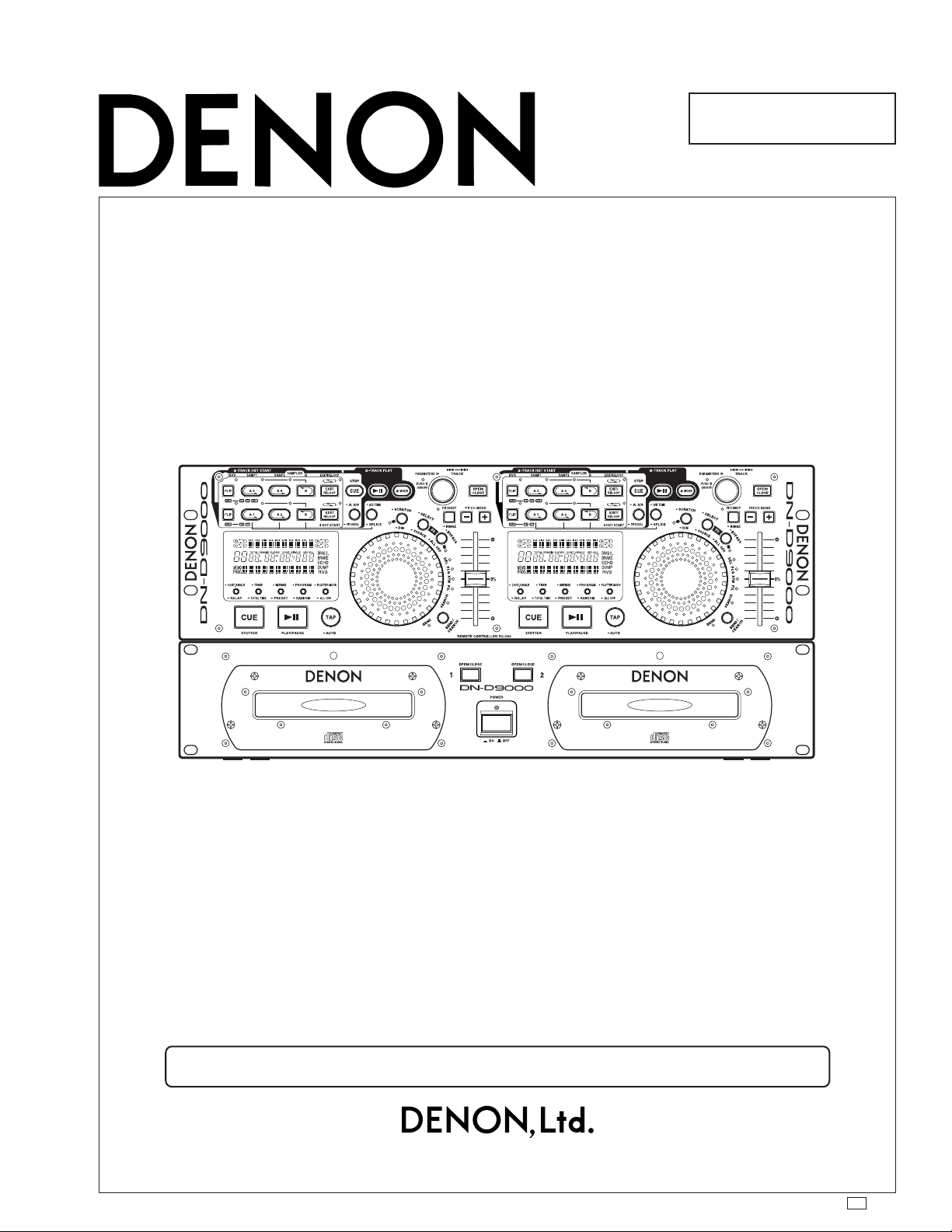
SERVICE MANUAL
For U.S.A., Canada,
Europe & Asia model
Hi-Fi Component
MODEL
DOUBLE CD PLAYER
DN-D9000
Some illustrations using in this service manual are slightly different from the actual set.
16-11, YUSHIMA 3-CHOME, BUNKYOU-KU, TOKYO 113-0034 JAPAN
Telephone: 03 (3837) 5321
X0139 NC 0203

SAFETY PRECAUTIONS
The following check should be performed for the continued protection of the customer and service technician.
LEAKAGE CURRENT CHECK
Before returning the unit to the customer, make sure you make either (1) a leakage current check or (2) a line to chassis
resistance check. If the leakage current exceeds 0.5 milliamps, or if the resistance from chassis to either side of the
power cord is less than 460 kohms, the unit is defective.
SPECIFICATIONS
GENERAL
Type: Twin mechanism compact disc player with wired remote control
Disc Type: Standard compact discs (12 cm and 8 cm discs)
For CD-R and CD-RW discs, only finalized ones can be played back.
However, some discs may not be playable depending on their recording
conditions.
Dimensions: Player unit: 482 (W) × 88 (H) × 252 (D) mm (without feet)
18-31/32" (W) × 3-15/32" (H) × 9-59/64" (D)
Remote control unit: 482 (W) × 62 (H) ×40 (D) mm (without feet)
18-31/32" (W) × 2-7/16" (H) × 1-37/64" (D)
Installation: 19-inch rack mountable
Player unit: 2U
Remote control unit: 3U
Player unit: 8 kg (17 lbs. 10.2oz)
Remote control unit: 4 kg (8 lbs. 13.1oz)
Power Supply: U.S.A. & Canada model: 120 V AC ±10 %, 60 Hz
Europe & Asia model: 230 V AC ±10 %, 50 Hz
Power Consumption: 33 W
Environmental Conditions: Operational temperature: 5 to 35 °C (41 to 95 °F)
Operational humidity: 25 to 85 % (no condensation)
Storage temperature: −20 to 60 °C (4 to 140 °F)
DN-D9000
AUDIO SECTION
Main out/Monitor out
Quantization: 24-bit linear per channel
Sampling Frequency: 44.1 kHz at normal pitch
Oversampling Rate: 8 times
Total Harmonic Distortion: ±0.01 % or less
S/N Ratio: 90 dB or more
Channel Separation: 85 dB or more
Frequency Response: 20 to 20,000 Hz
Analog output
Main Out Level: 2.0 Vrms
Monitor Out Level: 2.0 Vrms
Digital Output:
Signal Format: SPDIF (−6 dB)
Output Level: 0.5 Vp-p 75 Ω/ohms
Load Impedance: 10 kΩ/kohms or more
FUNCTIONS
Instant Start: Within 20 msec.
Variable Pitch
Main, α Track: ±4 % (0.05 % pitch), ±10 % (0.1 % pitch), ±16 % (0.1 % pitch),
±24 % (0.1 % pitch), ±100 % (1 % pitch)
Pitch Bend: Pitch range: ±4 %, ±10 % : ±12 %
Pitch range: ±16 %, ±24 % : ±26 %
Pitch range: ±100 % : ±99 %
SAMPLER
Sampling: 44.1 kHz
Length: 15 sec
Output Level: 2.0 Vrms (Variable/−14~+6 dB)
Variable Pitch: ±24 % (0.1 % pitch)
Search Precision: 1/75 sec (1 subcode frame)
Max. Scan Speed: Over 20 times normal speed
Max. Memo Memory Steps: 5,000 steps
2
DISASSEMBLY
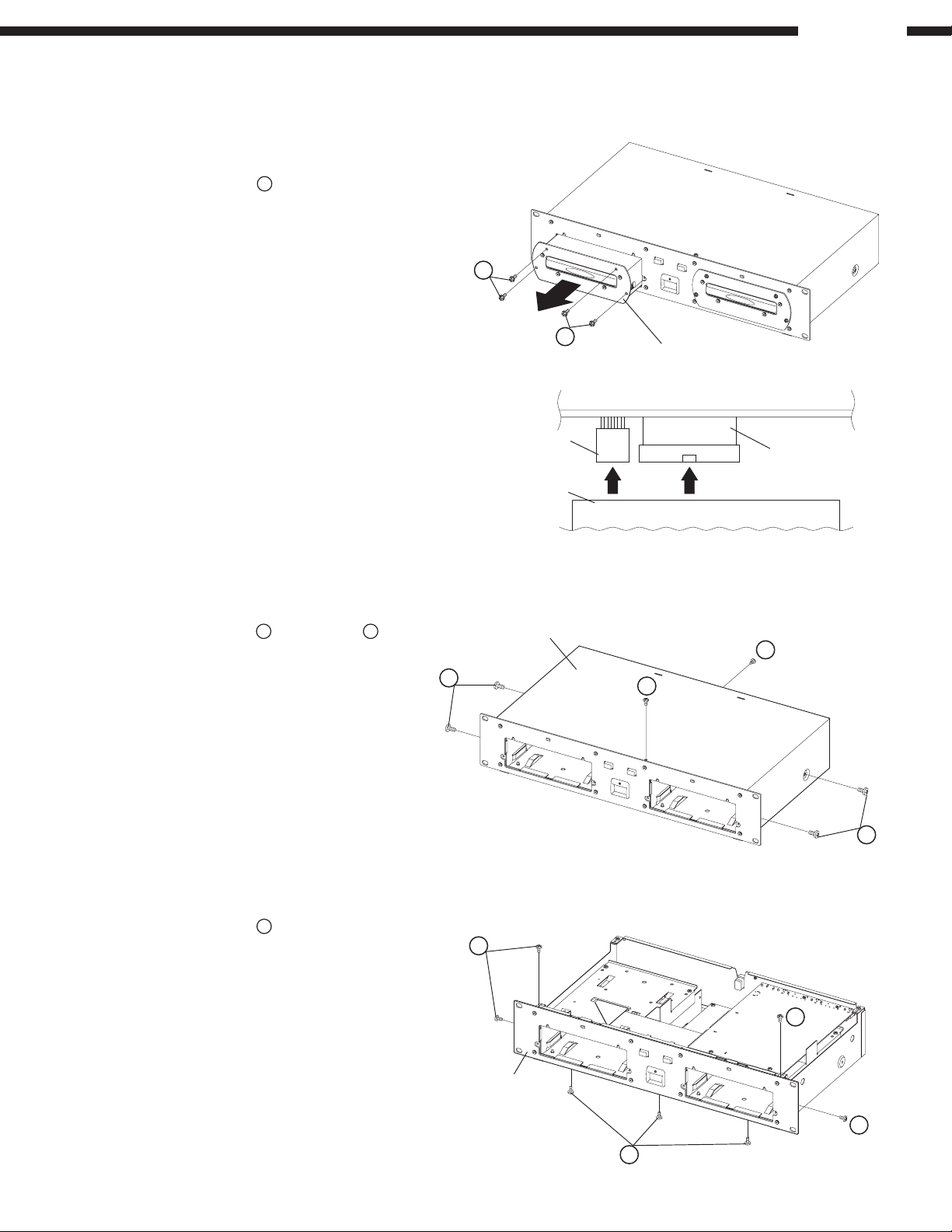
(Follow the procedure below in reverse order when reassembling)
Main Unit
1. Drive Unit
1) Remove 4 screws 1 and pull out Drive Unit.
2) Disconnect Flat cable and Connector.
3) Detach Drive Unit.
1
Note:
• Pull at a straight angle to avoid Flat Cable damage.
• Do not fail to pull AC cord from wall outlet before disconnect
the Flat Cable and Connector. If AC cord is remained
plugged into wall outlet, power is kept supplied in the unit,
which may cause danger.
DN-D9000
1
Drive Unit
Connector
Flat Cable
Drive Unit
2. Top Cover
1) Remove 4 screws 2 and 2 screws 3.
2) Detach Top Cover.
3. Front Panel Unit
1) Remove 7 screws 4 and pull out Front Panel Unit.
Top Cover
3
2
4
3
2
4
Front Panel Unit
4
4
3
DN-D9000
5
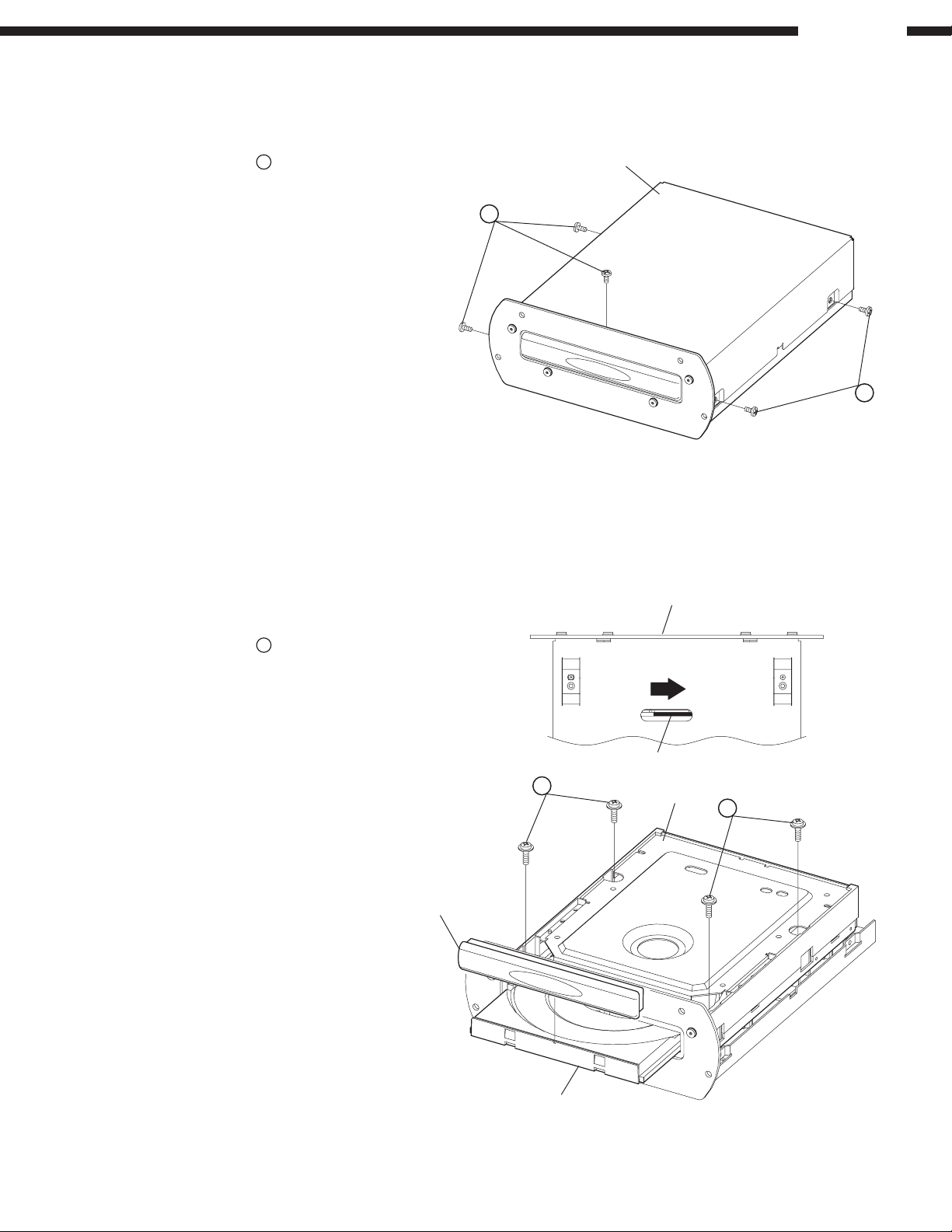
4. Drive Cover
1) Remove 5 screws 5 and pull out Drive Cover.
5. Drive
1) Move Drive Rack in arrow direction through the hole on
the bottom chassis. Loader Frame comes out.
2) Pull up Loader Panel while pulling it towards front.
6
3) Remove 4 screws
and pull out Drive.
Drive Cover
5
Drive Panel
Loader Panel
6
Loader Frame
Drive Rack
Drive
6
4
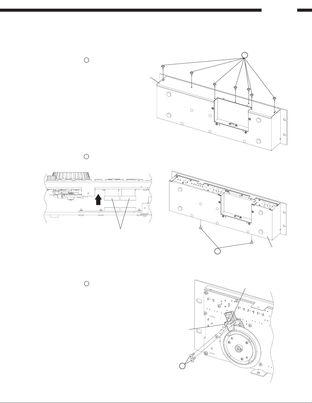
Remote Control Unit
1. Top Cover
1) Remove 7 screws 7 and pull out Top Cover.
2. Cover
1) Disconnect Connector.
2) Remove 2 screws 8 and pull out Cover.
DN-D9000
7
Top Cover
Connector
3. Sensor Unit
1) Remove 2 screws 9 and pull out Sensor Cover.
2) Detach Sensor Unit.
Sensor Cover
9
8
Sensor Unit
Cover
5
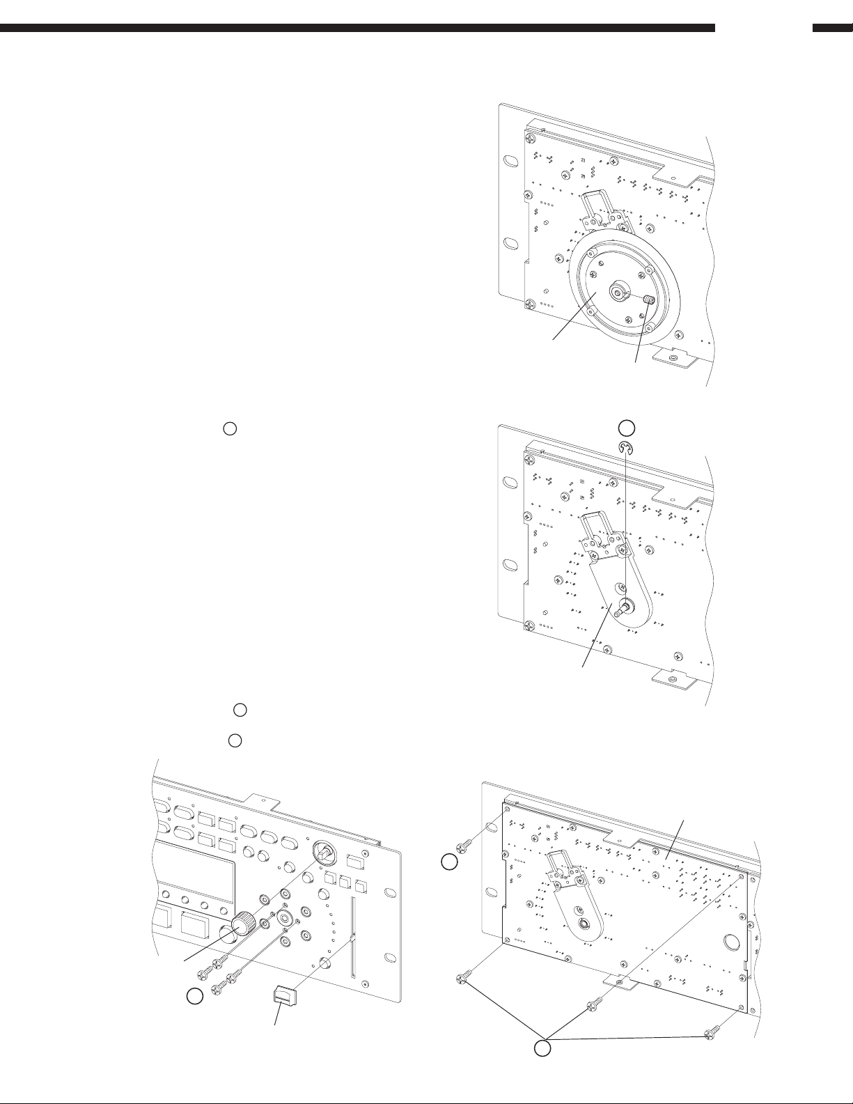
4. Wheel Unit
1) Remove Set Screw and pull out Wheel Unit.
5. Jog Dial Unit
1) Remove a E ring and pull out Jog Dial Unit.
DN-D9000
Wheel Unit
Set Screw
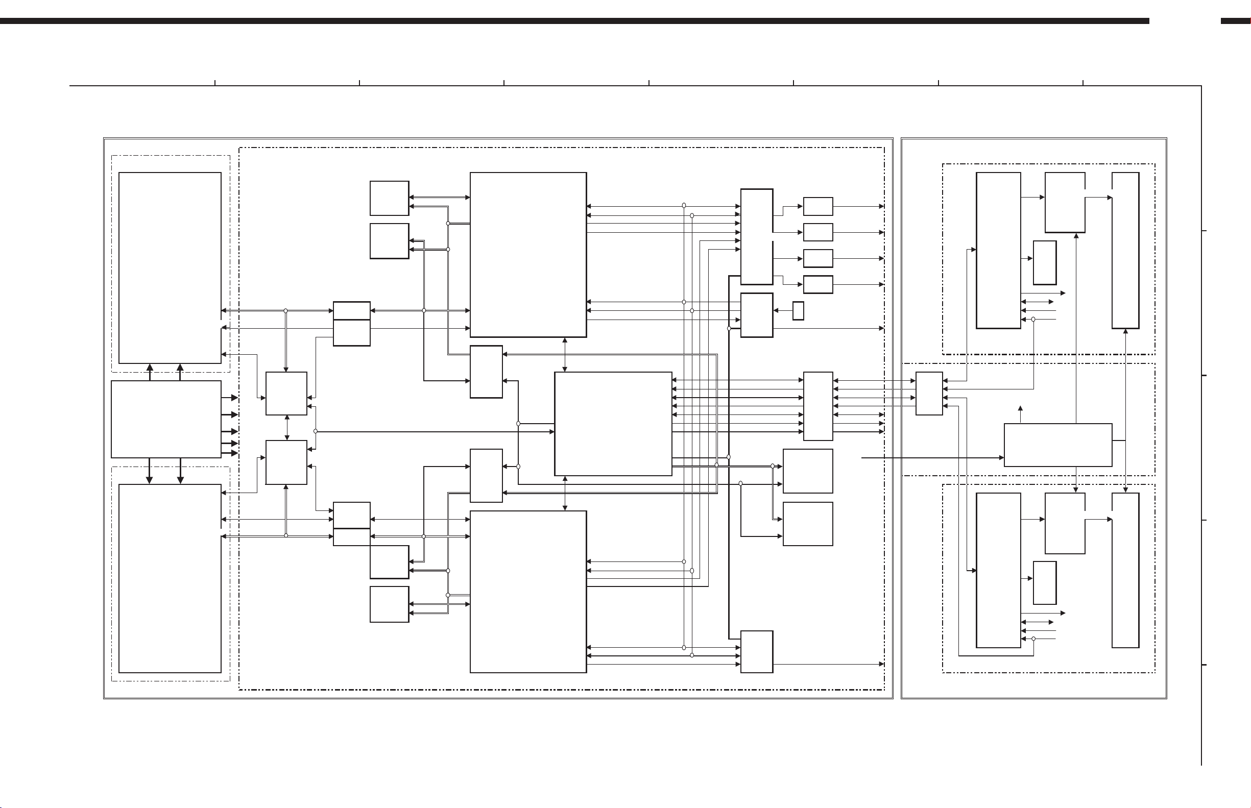
6. Inner Panel Unit
1) Remove 4 screws and pull out Knob (MARU) and
Fader Knob.
2) Remove 4 screws and pull out Inner Panel Unit.
Knob (MARU)
Fader Knob
Jog Dial Unit
Inner Panel Unit
6
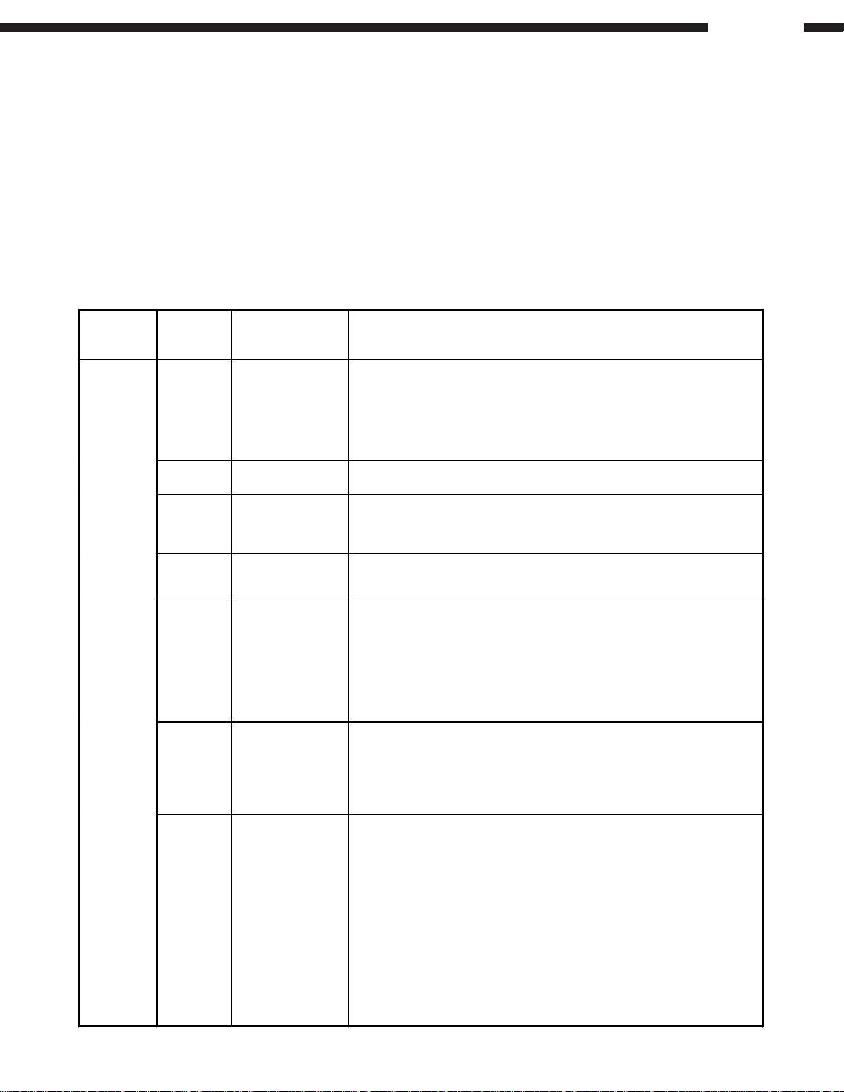
BLOCK DIAGRAM
RC-D90DN-D9000
CD1
FL tube out
TFS0
LRCK
main1 out
FLT Driver
ML9207
TCK0
BCLK
AMP10
FG-9000
ADDRESS
TXD0A
MAIN1
8
CH
CD1
DRIVE1
TXD0B
MON1
D/A
mon1 out
PCM1608 AMP11
ATAPI
INTERFACE
main2 out
AMP20
mon2 out
AMP21
TMP86CM47U
ROM32k
RAM1k
LED out
Key scan
16Bit Bus
TCK1
DIT
VR in
ATAPI
BUS
select
TXD1A
DOUT1
SM5902
JOG
interface
digital out
CPU DSP
BUS
8bit Bus
interface RC1
12V 5.0V
JOG1
DRIVER
JOG1
DRIVER
5.0V
RC2
JOG2
JOG2
3.3V
X’EFFECT
Data0~7
FADER1
5.0V HB
8.0V
FADER2
F1/F2
–12.0V
12V 5.0V
8.0V
CPU DSP
address
CD2
BUS
HB
interface
data
4M
MEMO
FL tube out
ATAPI
FLASH MEMORY
FG-9000
interface
DRIVE2
16Bit Bus
ATAPI
TFS0
LRCK
INTERFACE
TCK0
BCLK
TXD0A
MAIN2
TXD0B
MON2
ADDRESS
TMP86CM47U
ROM32k
RAM1k
LED out
Key scan
VR in
JOG
TFS1
DIT2
TCK1
SM5902
TXD1A
DOUT2
digital out
128MB
SDRAM
128MB
SDRAM
LEDdrive
BU2090
FLT1
384fs
DMA
ATAP
Interface
CPU
SYSTEM
CPU
TMP86CM47U
MN102H730F
RAM10K
RC/FLT Power
DC-DC Converter
ATAP
Interface
CPU
TMP86CM47U
4M
FLASH MEMORY
(DSP BOOT)
DMA
128MB
FLT2
ADSP21065L
SDRAM
DSP2
RAM Control
EFFECTOR
SHOCK PROOF
128MB
SDRAM
+12.0V
SWITCHING
REGULATOR
BUS
select
D0~D15
D16~D31
RAM Control
EFFECTOR
ADSP21065L
DSP1
SHOCK PROOF
D6~D31
D0~D15
TFS1
COM1
COM2
COM3
Control
Signal
Address
COM4
µcom
FLT Driver
ML9207
CD1
µcom
8bit Bus
LEDdrive
BU2090
DN-D9000
1 5678
32
4
A
B
C
D
E
7
CONFIRMING THE SERVO
Required Measuring Implement
1. Reference disc (TCD784 or CO-74176)
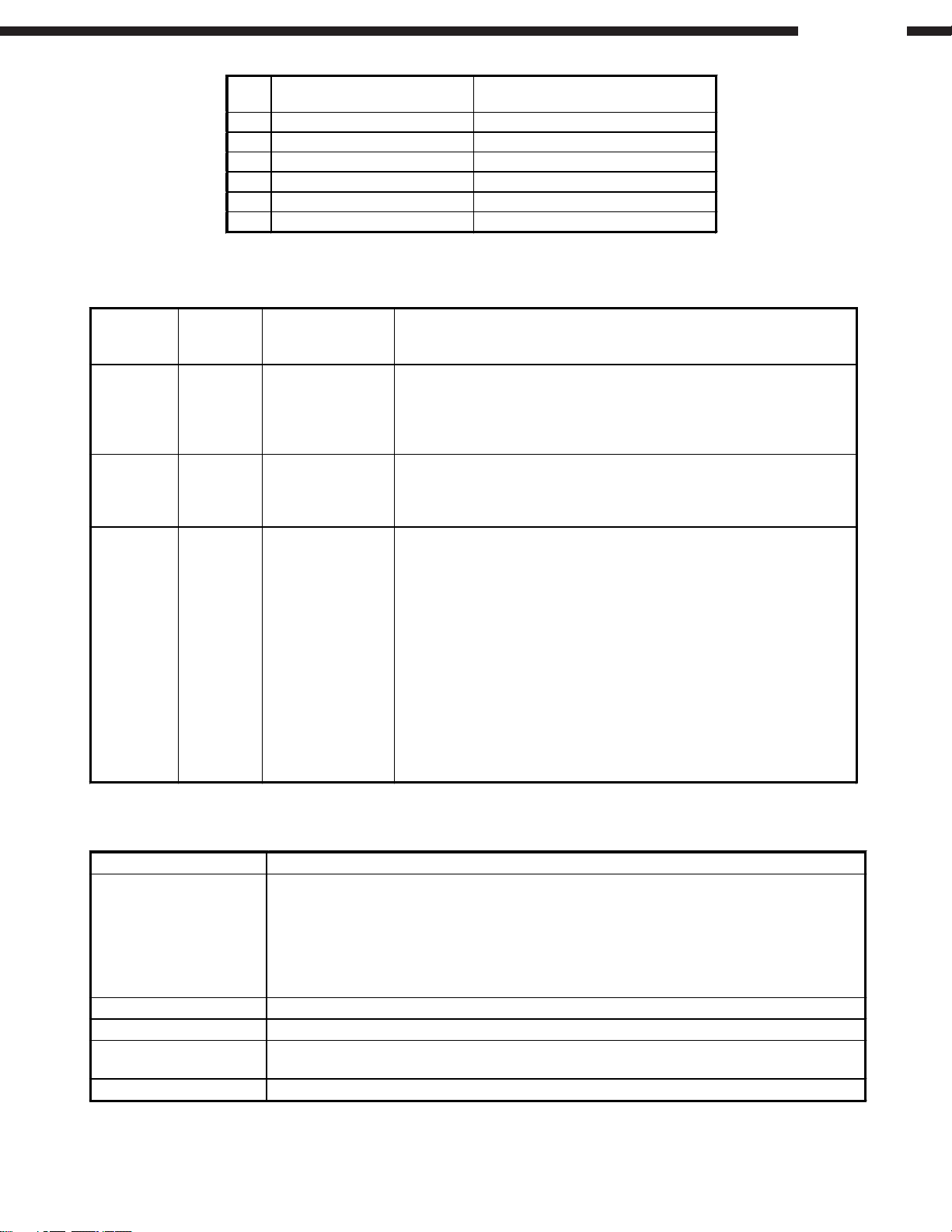
1. What is Service Program
Service program is a special program intended for confirming servo functions etc.
2. Contents of Service Program
Switch on the power while pushing the CD1’s PITCH BEND + button and CD2’s α CUE button at the same time. After
actuating the servo program, select an aiming process number with the SELECT knob, A1 button, A2 button, or A3 button.
Press the SELECT knob to execute the selected process, the process number is then displayed on the track indicator of the
display. To exit from the service program, just switch off the power.
DN-D9000
SELECT knob
Process No.
(TRACK
Indication)
01
02
03
04
05
06
07
Function
(Character-display)
Pcom Version check
(Version No.)
OPEN/CLOSE
(Open Close)
Drive Diagnostic
(Drive_Diag)
Drive Data Read
(Data Read)
Error Code Check
(Error Data)
Total Running Time
(Total_Time)
Automatic
Servo Adjustment
call
Contents
Check Version with JOG dial.
1. System Pcom version No.: “Sys_XXXX”
2. DSP soft version No.: “Dsp_XXXX”
3. ATAPI Pcom version No.: “Atapi_XXXX”
4. RC Pcom version No.: “Rc_XXXX”
5. ROM drive mecha. Pcom version No.: “Drive_XXXX”
Performs open/close each time when the SELECT knob is pushed.
ROM drive performs operation check when the SELECT knob is pushed, and
indicates the operational result. If the disc holder open, it starts the operation check
after closing. It indicates “Normal_End” if it ends normal. In case of error, ROM
drive error code is displayed in the character’s lower portion as “E”.
Starts continuous playback at its maximum reading speed from the beginning of
disc when the SELECT knob is pushed. It halts reading and stops if the knob is
pushed again.
Turn the JOG dial to display the logging error codes in the occurred order.
(“Error Data” is displayed.)
10 error logs are memorized at maximum.
Kinds of Error Code, displayed
Error Code Table (Appears only at Heat Run and Chucking Test function)
Pressing SELECT knob enters to data erase mode. (“Err Clear?” is displayed.)
If the SELECT knob is pushed again, the memorized error data are cleared.
Total time span of servo function that counted by the hour is displayed.
(“Total Time” is displayed.)
The display time is less than 65535 hours.
Note: No time is counted if powered down within 59 minutes.
Pressing SELECT knob enters to data erase mode. (“Time Clear?” is displayed.)
If the SELECT knob is pushed again, the memorized time data are cleared.
Starts automatic servo adjustment when the SELECT knob is pushed, and after
completing the adjustment, sort of the used disc is indicated. Data is selectable with
the JOG dial.
1. Disc check, CD/CD-RW
2. Focus gain data
3. Focus balance data
4. Focus offset data
5. Tracking gain data
6. Tracking balance data
7. Tracking offset data
8. PreAMP Tracking Sensor Gain
9. DSP Tracking Sensor Gain
10. PI offset
8
DN-D9000
3. TEST MODE
Process No.
(TRACK
Indication)
A1 button
A2 button
A3 button
AdjustmentItem
Adjustment Valueindicationat
character portions.
1 Focus Gain 35 ~ 120
2 Focus Balance 20 ~ 20
3 Focus Offset 20 ~ 20
4 Tracking Gain 35 ~ 120
5 Tracking Balance 20 ~ 20
6 Tracking Offset 20 ~ 20
* Reference data.
Function
(Character-display)
Starting with the PLAY/PAUSE button, it repeats open/close of the tray and
Heat Run
(H/R1_Normal)
Chucking Test
(H/R2_Tray)
System check
(Sys._Check)
playback.
All tracks are played back if the track count is less than 20. Only the first and last
tracks are played back if the tracks are more than 21. When any errors, it stops
and indicates error code (see Error Code Table).
Starting with the PLAY/PAUSE button, it repeats open/close of the tray, servo on,
and TOC read.
The display shows the number of the tray operation. When any errors, it stops and
indicates error code (see Error Code Table).
It starts system check when the PLAY/PAUSE button is pushed, and indicates the
status by performing plain operational check in the system .
1. Communication judge between the system Pcom and DSP
2. DSP SDRAM write/read operation check
3. Communication judge between the system Pcom and ATAPI Pcom
4. Communication judge between the ATAPI Pcom and ROM drive
5. ROM drive operation check
6. D/A register write/read operation check
7. DIT register write/read operation check
After finishing the check, it indicates the result on the character display lower
portion.
When the 1. ~ 7. items are OK, their item numbers are indicated.
But if there is a NG item, its item number is not indicated.
Contents
4. Error Code Table (Appears only at Heat Run and Chucking Test function)
Error Code Contents
Automatic Adjustment Error
E1 00
E1 01
E1 03
E1 04
E1 05
E1 06
E2 02 Servo down during automatic adjustment
E3 00 Unable to read TOC
E4 00
E4 01
E5 00 Slide error
Unable to detect disc
Unable to adjust tracking offset
Unable to adjust focus fine gain
Unable to actuate focus
Unable to actuate tracking
Unable to adjust tracking fine gain
Unable to close the disc holder in the regular time
Unable to open the disc holder in the regular time
9
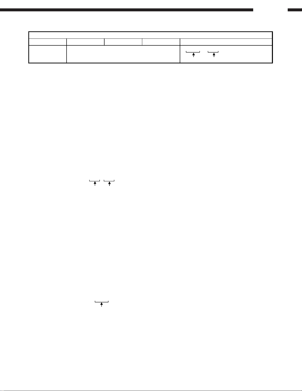
Detailed error can be displayed by JOG dial when error occurs.
Error Indication
TR MIN SEC FRAM CHARACTER
Displays the track
No. in which error
occurred.
Displays the time at which error occurred. “H uuuu E uuu”
DN-D9000
Operation count Error code
5. System
System µcom and DSP can be upgraded in the following manner.
Version Upgrade Method
1. Record the version upgrade software on a CD-R or CD-RW disc, only as one file with the format ISO9660 Mode-1.
2. After loading the disc made in above step 1 into CD1, turn off the power. Then, turn on the power while pressing the
3. TRAY LED of both CD1 and CD2 will turn on when the version upgrade starts, and they will turn off when the version
4. Turn off the power after finishing the version upgrade, and turn on again to take out the disc.
5. File name of the upgrade software indicates version numbers.
6. ROM Drive (FG-9000)
Drive (FG-9000) µcom can be upgraded in the following manner.
µµ
µcom and DSP Version Upgrade
µµ
The file name of the supplied version upgrade software should be used as is and this disc needs to finalize.
OPEN/CLOSE button of CD1. The version upgrade starts with reading data of the disc. No disc should be loaded into
CD2.
upgrade ends.
TRAY LED of both CD1 and CD2 will blink if the version upgrade ends abnormally due to error etc.
In case of some error or the power is turned off during the version upgrade, it may be impossible to operate at all
thereafter. Changing of IC502 on GU-3412 is necessary in this case, and software writing to IC502 should be done
beforehand.
File name D9 uuu uuu . BIN
System Pcom
version
DSP version
µµ
µcom Version Upgrade
µµ
Version Upgrade Method
1. Record the version upgrade software on a CD-R or CD-RW disc, only as one file with the format ISO9660 Mode-1.
The file name of the supplied version upgrade software should be used as is and this disc needs to finalize.
2. After turning on the power, load the disc made in above step 1 into the mecha. you want to upgrade the version.
3. “Drive” and “Version UP?” are indicated in the character display. Press the OPEN/CLOSE button and remove the disc
when not upgrade the version.
4. Press the PLAY/PAUSE to start the version upgrade. “Now Loading” is indicated.
5. When the version upgrade is finished, “Complete” is indicated and the tray opens.
6. Turn off the power once and turn on again after take out the disc.
The version upgrade ends in 20~30 seconds normally. If the power turned off underway or the version upgrade ends
abnormally, the drive may become malfunction. In such a case, version upgrade with PC will be needed.
7. File name of the upgrade software indicates version number.
File name FG9K uuuu . BIN
Version number
10
SEMICONDUCTORS
IC’s
Note: Indication before IC Numbers denotes P.W.B. name.
FG : CD-ROM P.W.B. Unit
DS : DSP P.W.B. Unit
PO : Power P.W.B. Unit
RC : Remote P.W.B. Unit
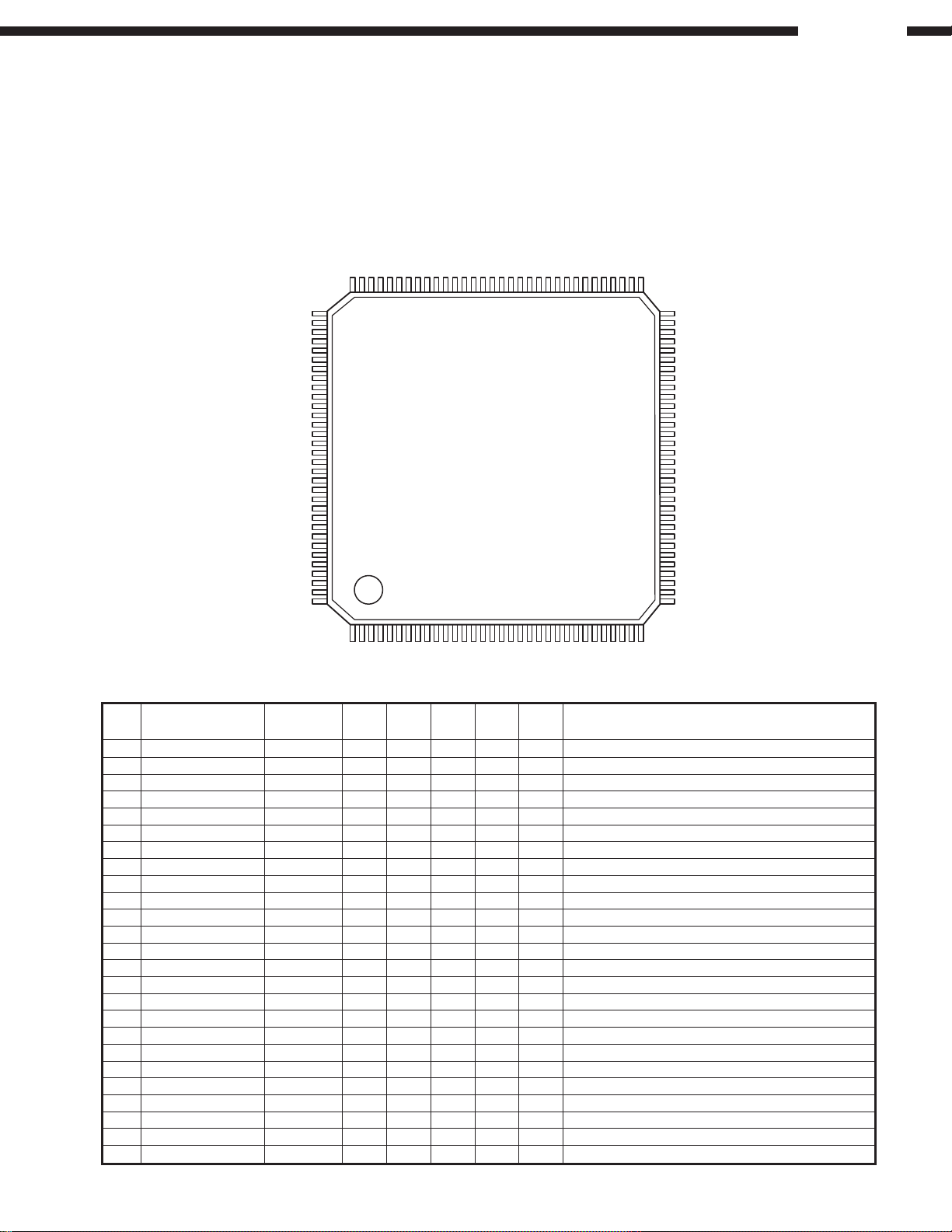
MN102H730F (DS: IC501)
96 65
97 64
TOP VIEW
DN-D9000
128 33
132
MN102H730F Terminal Function
Pin
No.
1 CS0_ CS0_ O — Pu — — Ext. memory chip select 0 (Flash ROM CS)
2 CS1_ CS1_ O — Pu — — Ext. memory chip select 1 (Flash ROM for memo)
3 D00 DQ0 I/O — — — — Ext. memory data in/output 0, DSP interface 0
4 D01 DQ1 I/O — — — — Ext. memory data in/output 1, DSP interface 1
5 D02 DQ2 I/O — — — — Ext. memory data in/output 2, DSP interface 2
6 D03 DQ3 I/O — — — — Ext. memory data in/output 3, DSP interface 3
7 VDD VDD — — — — — Power (+3.3V)
8 VSS VSS — — — — — GND
9 D04 DQ4 I/O — — — — Ext. memory data in/output 4, DSP interface 4
10 D05 DQ5 I/O — — — — Ext. memory data in/output 5, DSP interface 5
11 D06 DQ6 I/O — — — — Ext. memory data in/output 6, DSP interface 6
12 D07 DQ7 I/O — — — — Ext. memory data in/output 7, DSP interface 7
13 D08,P10 KEYIN2 I — Pu H H OPEN/CLOSE2 key input
14 D09,P11 KEYIN1 I — Pu H H OPEN/CLOSE1 key input
15 D10,P12 FPLAY1 I — Pu H H CD1 fader start PLAY input
16 PD0,DMAACK1_ FCUE1 I — Pu H H CD1 fader start CUE input
17 PD1,DMAREQ1_ FPLAY2 I — Pu H H CD2 fader start PLAY input
18 D11,P13 FCUE2 I — Pu H H CD2 fader start CUE input
19 D12,P14 JOGA2 I — (Pu) H H JOGA pulse input for CD2 scratch (Direction detect)
20 D13,P15 JOGB2 I — (Pu) H H JOGB pulse input for CD2 scratch (Direction detect)
21 D14,P16 JOGA1 I — Pu H H JOGA pulse input for CD1 scratch (Direction detect)
22 D15,P17 JOGB1 I — Pu H H JOGB pulse input for CD1 scratch (Direction detect)
23 WORD WORD I — — Data bus width select (H: 8bit), VDD fixed
24 VDD VDD — — — — — Power (+3.3V)
25 MODE MODE I — — L L Processor mode, GND fixed
Pin Name
Symbol
I/O
DET Ext Ini Res
Function
11

DN-D9000
Pin
No.
26 PC3 MUTE O — Pu H H Mute signal (H: Mute)
27 XI XI I — — — — Oscillation input
28 XO XO O — — — — Oscillation output
29 VDD VDD — — — — — Power (+3.3V)
30 OSCI OSCI I — — — — Oscillation input, 32.0MHz
31 OSCO OSCO O — — — — Oscillation output
32 VSS VSS — — — — — GND
33 BOSC 32.0MHz O — — — — System clock output
34 PC5,NMI_ RESERVE I — Pu H H
35 RST_ RST_ I — — — — µcom reset
36 PC0 LEDOUT1 O — Pu H H TRAY1 LED
37 P76 LEDOUT2 O — Pu H H TRAY2 LED
38 P60,IRQ0 JOGINT1 I — (Pu) H H JOGA pulse input for CD1 scratch
39 P61,IRQ1 JOGINT2 I — (Pu) H H JOGA pulse input for CD2 scratch
40 P62,IRQ2 DTIMA1 I — (Pu) H H CD1 main playback clock input
41 P63,IRQ3 DTIMB1 I — Pu H H CD1 monitor playback clock input
42 P64,IRQ4 ATANS_ I — Pu — H ATAPI µcom serial interface
43 P65,IRQ5 DTIMA2 I — Pu H H CD2 main playback clock input
44 P66,IRQ6 DTIMB2 I — Pu H H CD2 monitor playback clock input
45 P67,IRQ7 RESERVE O — — H —
46 P70 YMCLK O — — H — Clock for SM5902(DOUT)/PCM1608(D/A) data
47 P71 YMDATA O — — H — SM5902(DOUT)/PCM1608(D/A) output data
48 PD2,DMAACK0_ NRES_ O — Pd L L SM5902(DOUT)/PCM1608(D/A) reset signal
49 PD3,DMAREQ0_ ZSENCE1 I — — — — SM5902 µcom interface status for CD1
50 VDD VDD — — — — — Power (+3.3V)
51 P77 ZSENCE2 I — — — — SM5902 µcom interface status for CD2
52 P72 MDO I — Pd — L PCM1608(D/A) input data
53 P73 YMLD1_ O — — H — SM5902(DOUT) chip select for CD1
54 P74 YMLD2 O — — H — SM5902(DOUT) chip select for CD2
55 P75 ML O — — H — PCM1608(D/A) chip select
56 PA0,SBI0 RXD1 I — (Pu) — H Data receive from RC CD1
57 PA1,SBO0 TXD1 O — Pu H H Data send to RC CD1 (PU µcom specify)
58 PA2,SBT0 MCMD_ O — Pu H H ATAPI µcom serial interface (PU µcom specify)
59 PA3,SBI1 RXD2 I — (Pu) — H Data receive from RC CD2
60 PA4,SBO1 TXD2 O — Pu H H Data send to RC CD2
61 PA5 ATDIR O — — H — Not used
62 PB0,SBI2 X’RXD I — (Pu) — H Data receive from X’EFFECT
63 PB1,SBO2 X’TXD O — Pu H H Data send to X’EFFECT
64 PB2 APRES_ O — Pd L L ATAPI µcom reset signal (CD1, CD2 common)
65 PB3,SBI3 ATDATA I — Pu — H ATAPI µcom serial receive signal
66 PB4,SBO3 MDATA O — Pu H H ATAPI µcom serial send signal
67 PB5,SBT3 MCLK O — Pd H L ATAPI µcom serial send/receive clock
68 VDD VDD — — — — — Power (+3.3V)
69 VSS VSS — — — — — GND
70 AVSS AVSS — — — — — Analog ref. GND for A/D conversion, GND
71 Vref− Vref− — — — — — Analog ref. V for A/D conversion, GND
72 P80 DFLG12 I/O — Pu — H DSP1 general flag 2
73 P81 DFLG11 I/O — Pu — H DSP1 general flag 1
74 P82 DR_/W1 O — — H — DSP1 interface send/receive select signal
75 P83 DACK1_ I — Pu H H DSP1 interface ACK
76 P84 DBSY1_ I — Pu H H DSP1 interface busy signal
77 P85 DFLG10 I/O — Pu — H DSP1 general flag 0
78 P86 DREQ1_ O — (Pu) H H DSP1 interface request signal
79 P87 DR_/W2 O — — H — DSP2 interface send/receive select signal
80 PD4 DACK2_ I — Pu H H DSP2 interface ACK
81 PD5 DBSY2_ I — Pu H H DSP2 interface busy signal
82 P90 DFLG20 I/O — Pu — H DSP2 general flag 0
83 P91 DREQ2_ O — (Pu) H H DSP2 interface request signal
84 P92 DFLG21 I/O — Pu — H DSP2 general flag 1
85 P93 DFLG22 I/O — Pu — H DSP2 general flag 2
86 Vref+ Vref+ — — — — — Analog ref. V for A/D conversion, +3.3V
87 AVDD AVDD — — — — — Power (+3.3V)
Pin Name
Symbol
I/O
DET Ext Ini Res
Function
12
DN-D9000
Pin
No.
88 P94 RCRST_ O — Pd L L RCD90 reset signal (L: Reset)
89 P95 APOWER O — Pd L L Analog output voltage ON/OFF (L: OFF)
90 P96 RESERVE O — — H —
91 P97 RESERVE O — — H —
92 BREQ_ BREQ_ I — Pu H H Bus request signal
93 BRACK_ BRACK_ O — Pu H H Bus request accept signal
94 WEL_ WE_ O — Pu — H Ext. memory write enable (Lower 8bit)
95 P51 RESERVE O — — H —
96 RE_ RE_ O — Pu — H Ext. memory read enable
97 CS2_ CS2_ O — Pu — H Ext. memory chip select 2 (DSP1 interface)
98 VDD VDD — — — — — Power (+3.3V)
99 VSS VSS — — — — — GND
100 P54, BSTRE SAMPC1 O — Pu H H Not used
101 P55, WR_ SAMPC2 O — Pu H H Not used
102 CS3_ CS3_ O — Pu — H Ext. memory chip select 3 (DSP2 interface)
103 A00 A00 O — — — — Ext. memory address bus 0
104 A01 A01 O — — — — Ext. memory address bus 1
105 A02 A02 O — — — — Ext. memory address bus 2
106 A03 A03 O — — — — Ext. memory address bus 3
107 A04 A04 O — — — — Ext. memory address bus 4
108 A05 A05 O — — — — Ext. memory address bus 5
109 A06 A06 O — — — — Ext. memory address bus 6
110 A07 A07 O — — — — Ext. memory address bus 7
111 A08 A08 O — — — — Ext. memory address bus 8
112 PD6 RESERVE O — — L —
113 PD7 RESERVE O — — L —
114 A09 A09 I — — — — Ext. memory address bus 9
115 A10 A10 I — — — — Ext. memory address bus 10
116 A11 A11 O — — — — Ext. memory address bus 11
117 A12 A12 O — — — — Ext. memory address bus 12
118 A13 A13 O — — — — Ext. memory address bus 13
119 VDD VDD — — — — — Power (+3.3V)
120 PC4 RESERVE O — — L —
121 A14 A14 O — — — — Ext. memory address bus 14
122 A15 A15 O — — — — Ext. memory address bus 15
123 A16 A16 O — — — — Ext. memory address bus 16
124 A17 A17 O — Pu — — Ext. memory address bus 17
125 A18 A18 O — Pu — — Ext. memory address bus 18
126 A19 A19 O — Pu — — Ext. memory address bus 19
127 A20 A20 O — Pu — — Ext. memory address bus 20
128 A21 A21 O — Pu — — Ext. memory address bus 21
Pin Name
Symbol
I/O
DET Ext Ini Res
Function
13
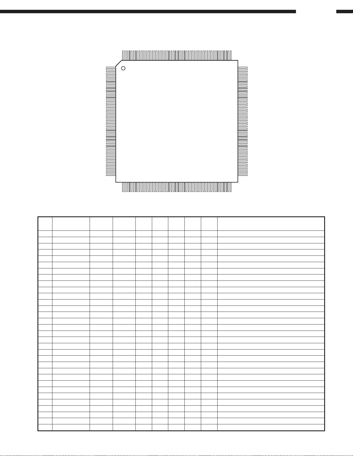
ADSP-21065L (DS: IC301, 401)
DN-D9000
208 157
1
156
TOP VIEW
52
53
104
105
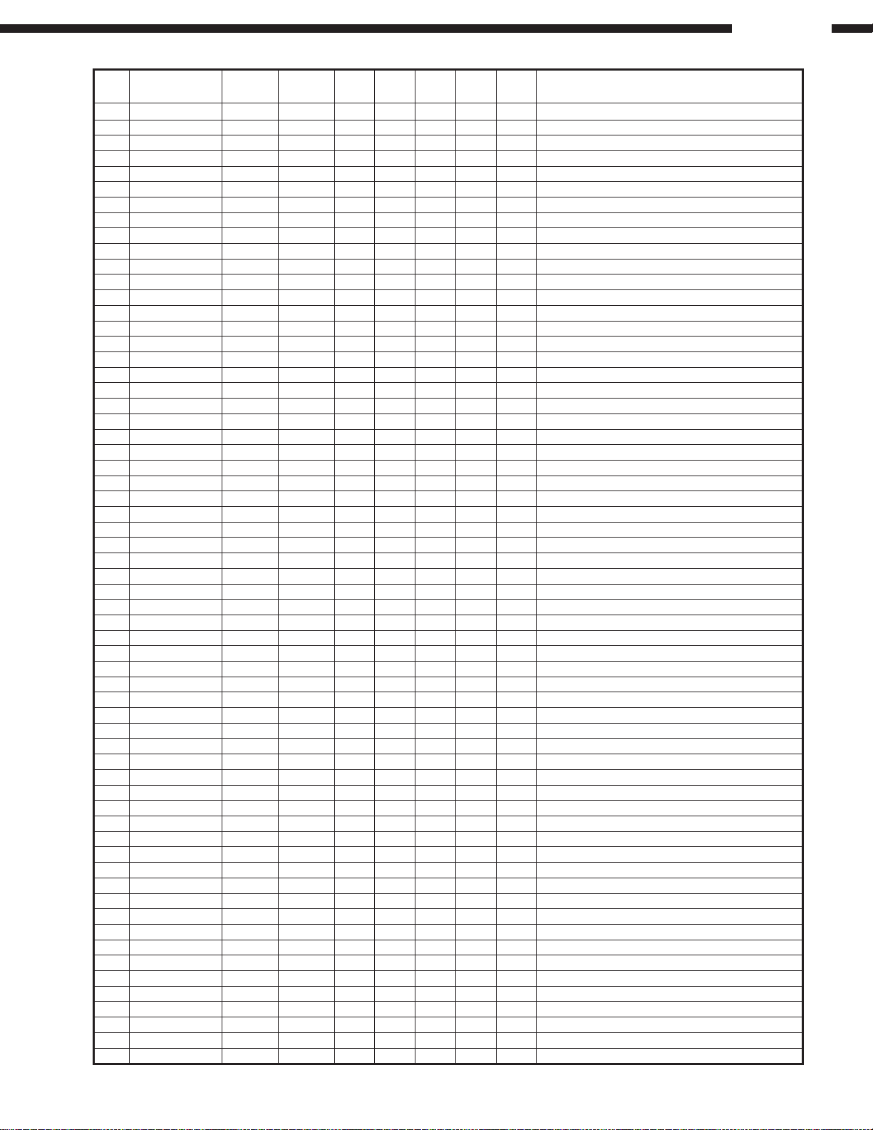
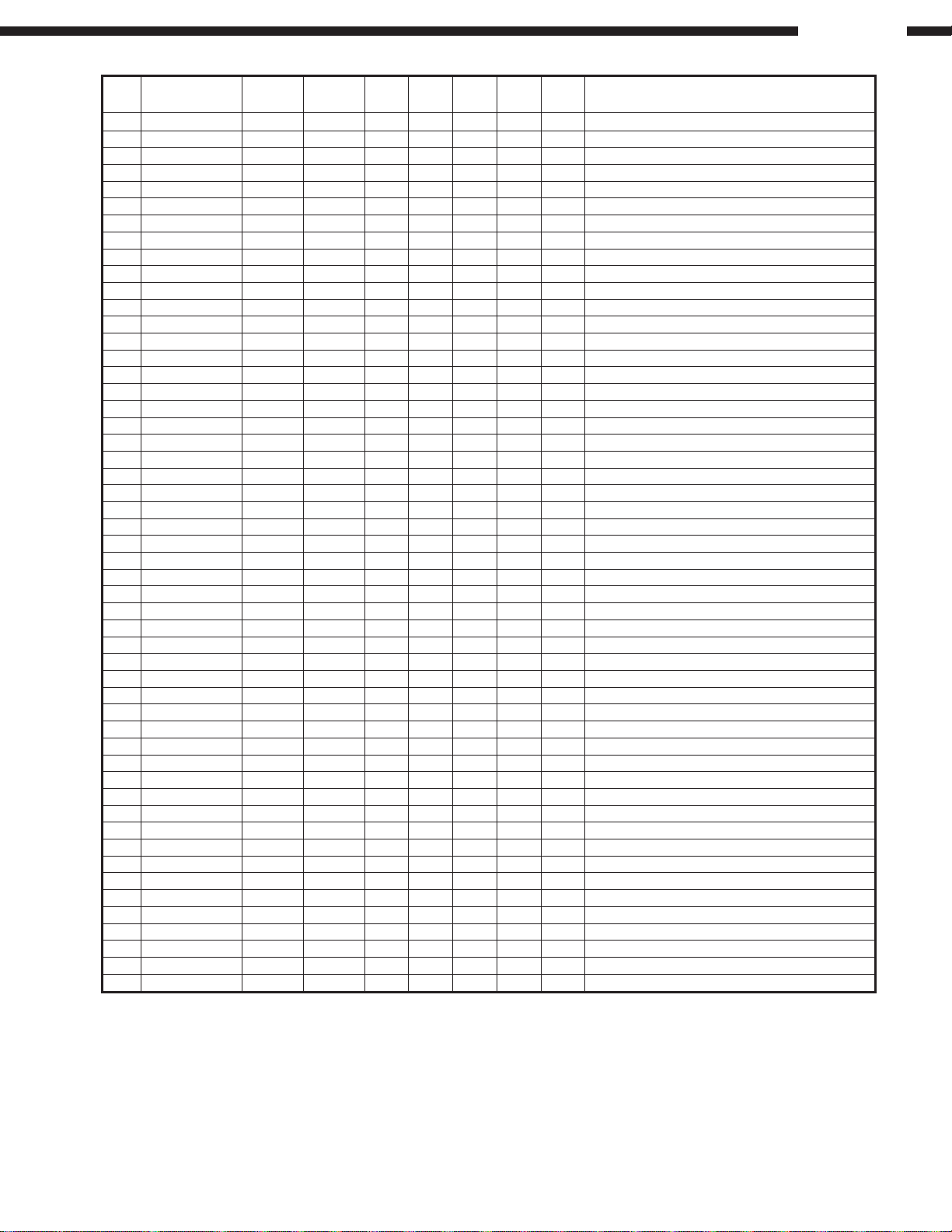
ADSP-21065L Terminal Function
Pin
No.
1 VDD VDD VDD — — — — — Power (+3.3V)
2 RFS0 YLRCK YLRCK I — IPu — H
3 GND GND GND — — — — — GND
4 RCLK0 YBCK YBCK I — — — — Receive frame sync (BCK) signal (Serial port IN 0)
5 DR0A ADDATA ADDATA I — IPu — H Data receive A (serial port IN 0)
6 DR0B I — IPu — H Data receive B (serial port IN 0)
7 TFS0 YLRCK YLRCK I — IPu — H
8 TCLK0 YBCK YBCK I — — — — Send frame sync (BCK) signal (Serial port OUT 0)
9 VDD VDD VDD — — — — — Power (+3.3V)
10 GND GND GND — — — — — GND
11 DT0A MOUT1 MOUT2 O — IPu — H Data send A (Serial port OUT 0)
12 DTOB DOUT1 DOUT2 O — IPu — H Data send B (Serial por t OUT 0)
13 RFS1 LRCK1 LRCK2 I — IPu — H
14 GND GND GND — — — — — GND
15 RCLK1 BCK1 BCK2 I — — L — Receive frame sync (BCK) signal (Serial port IN 1)
16 DR1A SAMP2 SAMP1 I — IPu — H Data receive A (serial port IN 1)
17 DR1B I — IPu — H Data receive B (serial port IN 1)
18 TFS1 LRCK2 LRCK1 I/O — IPu — H
19 TCLK1 BCK2 BCK1 I/O — — — — Send frame sync (BCK) signal (Serial port OUT 1)
20 VDD VDD VDD — — — — — Power (+3.3V)
21 VDD VDD VDD — — — — — Power (+3.3V)
22 DT1A SOUT1 SOUT2 O — IPu — H Data send A (Serial por t OUT 1)
23 DT1B SAMP1 SAMP2 O — IPu — H Data send B (Serial port OUT 1)
24 PWM_EVENT1 I/O — Pd — L PWM1 output
25 GND GND GND — — — — — GND
26 PWM_EVENT0 I/O — Pd — L PWM0 output
27 BR1_ I — Pu — H Multi-processing bus request 1
28 BR2_ I — Pu — H Multi-processing bus request 1
29 VDD VDD VDD — — — — — Power (+3.3V)
30 CLKIN I — — — — Clock input
31 XTAL_ O — — — — X’tal oscillator pin
32 VDD VDD VDD — — — — — Power (+3.3V)
Port Name
Symbol
(IC301)
Symbol
(IC401)
I/O DET Ext Ini
Res
Receive frame sync (LRCK) signal (Serial port IN 0)
Send frame sync (LRCK) signal (Serial port OUT 0)
Receive frame sync (LRCK) signal (Serial port IN 1)
Send frame sync (LRCK) signal (Serial port OUT 1)
Function
14
DN-D9000
Pin
No.
33 GND GND GND — — — — — GND
34 SDCLK1 O — Pd — L SDRAM clock enable 1
35 GND GND GND — — — — — GND
36 VDD VDD VDD — — — — — Power (+3.3V)
37 SDCLK0 I/O — — — — SDRAM clock enable 0
38 DMAR1_ I — Pu H H DMA request 1
39 DMAR2_ I — Pu H H DMA request 2
40 HBR_ I — Pu — H Host bus request (BOOT)
41 GND GND GND — — — — — GND
42 RAS_ I/O — Pu H H SDRAM row access strobe
43 CAS_ I/O — Pu H H SDRAM column access strobe
44 SDWE_ I/O — Pu H H SDRAM write enable
45 VDD VDD VDD — — — — — Power (+3.3V)
46 DQM O — — — — SDRAM data mask
47 SDCKE I/O — — H — SDRAM clock enable
48 SDA10 O — Pd L L SDRAM A10
49 GND GND GND — — — — — GND
50 DMAG1_ O — — H — DMA ground 1
51 DMAG2_ O — — H — DMA ground 2
52 HBG_ O — — H — Host bus ground (BOOT)
53 BMSTR O — — H — Bus master output (H out)
54 VDD VDD VDD — — — — — Power (+3.3V)
55 CS_ I — — L L Chip select (BOOT)
56 SBTS_ I — Pu H H Extend bus three state
57 GND GND GND — — — — — GND
58 WR_ I/O — — — — Memor y write strobe
59 RD_ I/O — — — — Memory read strobe
60 GND GND GND — — — — — GND
61 VDD VDD VDD — — — — — Power (+3.3V)
62 GND GND GND — — — — — GND
63 REDY O — — — — Host bus ACK
64 SW_ I/O — — — — Sync type write select
65 CPA_ I/O — — — — Core priority access
66 VDD VDD VDD — — — — — Power (+3.3V)
67 VDD VDD VDD — — — — — Power (+3.3V)
68 GND GND GND — — — — — GND
69 ACK I/O — — — — Memory ACK
70 MS0_ I/O — Pu H H Memory select 0
71 MS1_ I/O — — — — Memory select 1
72 GND GND GND — — — — — GND
73 GND GND GND — — — — — GND
74 MS2_ I/O — — — — Memory select 2
75 MS3_ I/O — — — — Memory select 3
76 FLAG11
77 VDD VDD VDD — — — — — Power (+3.3V)
78 FLAG10
79 FLAG9 JOGB1 JOGB2 I — — — —
80 FLAG8 JOGA1 JOGA2 I — — — —
81 GND GND GND — — — — — GND
82 DATA0 I/O — — — — Ext. bus data 0
83 DATA1 I/O — — — — Ext. bus data 1
84 DATA2 I/O — — — — Ext. bus data 2
85 VDD VDD VDD — — — — — Power (+3.3V)
86 DATA3 I/O — — — — Ext. bus data 3
87 DATA4 I/O — — — — Ext. bus data 4
88 DATA5 I/O — — — — Ext. bus data 5
89 GND GND GND — — — — — GND
90 DATA6 I/O — — — — Ext. bus data 6
91 DATA7 I/O — — — — Ext. bus data 7
92 DATA8 I/O — — — — Ext. bus data 8
93 VDD VDD VDD — — — — — Power (+3.3V)
94 GND GND GND — — — — — GND
Port Name
Symbol
(IC301)
DMABSY1
SAMPCOP
Symbol
(IC401)
DMABSY2
SAMPCOPY
I/O DET Ext Ini
O — Pu — H General flag 11 (In DMA flag L: DMA)
I/O — Pu — H General flag 10 (In SAMPLER copy flag)
Res
General flag 9 (JOG turning direction detect signal B)
General flag 8 (JOG turning direction detect signal A)
Function
15

DN-D9000
Pin
No.
95 VDD VDD VDD — — — — — Power (+3.3V)
96 DATA9 I/O — — — — Ext. bus data 9
97 DATA10 I/O — — — — Ext. bus data 10
98 DATA11 I/O — — — — Ext. bus data 11
99 GND GND GND — — — — — GND
100 DATA12 I/O — — — — Ext. bus data 12
101 DATA13 I/O — — — — Ext. bus data 13
102NC —————NC
103NC —————NC
104 DATA14 I/O — — — — Ext. bus data 14
105 VDD VDD VDD — — — — — Power (+3.3V)
106 GND GND GND — — — — — GND
107 DATA15 I/O — — — — Ext. bus data 15
108 DATA16 I/O — — — — Ext. bus data 16
109 DATA17 I/O — — — — Ext. bus data 17
110 VDD VDD VDD — — — — — Power (+3.3V)
111 DATA18 I/O — — — — Ext. bus data 18
112 DATA19 I/O — — — — Ext. bus data 19
113 DATA20 I/O — — — — Ext. bus data 20
114 GND GND GND — — — — — GND
115NC —————NC
116 DATA21 I/O — — — — Ext. bus data 21
117 DATA22 I/O — — — — Ext. bus data 22
118 DATA23 I/O — — — — Ext. bus data 23
119 GND GND GND — — — — — GND
120 VDD VDD VDD — — — — — Power (+3.3V)
121 DATA24 I/O — — — — Ext. bus data 24
122 DATA25 I/O — — — — Ext. bus data 25
123 DATA26 I/O — — — — Ext. bus data 26
124 VDD VDD VDD — — — — — Power (+3.3V)
125 GND GND GND — — — — — GND
126 DATA27 I/O — — — — Ext. bus data 27
127 DATA28 I/O — — — — Ext. bus data 28
128 DATA29 I/O — — — — Ext. bus data 29
129 GND GND GND — — — — — GND
130 VDD VDD VDD — — — — — Power (+3.3V)
131 VDD VDD VDD — — — — — Power (+3.3V)
132 DATA30 I/O — — — — Ext. bus data 30
133 DATA31 I/O — — — — Ext. bus data 31
134 FLAG7 DFLG12 DFLG22 I/O — Pu — H General flag 7 (RESERVE)
135 GND GND GND — — — — — GND
136 FLAG6 DFLG11 DFLG21 I/O — Pu — H General flag 6 (RESERVE)
137 FLAG5 DTIMB1 DTIMB2 O — — — —
138 FLAG4 DTIMA1 DTIMA2 O — — — —
139 GND GND GND — — — — — GND
140 VDD VDD VDD — — — — — Power (+3.3V)
141 VDD VDD VDD — — — — — Power (+3.3V)
142NC —————NC
143 ID1 I — — L L Multi-processing ID1 (Single processor: 0)
144 ID0 I — — L L Multi-processing ID2 (Single processor: 0)
145 EMU_ EMU1_ EMU2_ O — — — — Emulation status
146 TD0 TD01 TD02 O — — — — Test data output (JTAG)
147 TRST_ TRST1_ TRST2_ I — IPu — H Test reset (JTAG)
148 TDI TDI1 TDI2 I — Pd — L Test data input (JTAG)
149 TMS TMS1 TMS2 I — IPu — H Test mode select (JTAG)
150 GND GND GND — — — — — GND
151 TCK TCK1 TCK2 I — Pu — H Test clock (JTAG)
152 BSEL I — — H H EPROM boot select (Boot by EPROM: 1)
153 BMS_ BMS1_ BMS2_ I — — H H Boot memory select (Host processor boot: 1)
154 GND GND GND — — — — — GND
155 GND GND GND — — — — — GND
156 VDD VDD VDD — — — — — Power (+3.3V)
Port Name
Symbol
(IC301)
Symbol
(IC401)
I/O DET Ext Ini
Res
General flag 5 (Pulse output for generating monitor play time)
General flag 4 (Pulse output for generating main play time)
Function
16
DN-D9000
Pin
No.
157 RESET_ DRES_ DRES_ I — — H L DSP reset signal
158 VDD VDD VDD — — — — — Power (+3.3V)
159 GND GND GND — — — — — GND
160 ADDR23 I/O — — — — Ext. bus address 23
161 ADDR22 I/O — — — — Ext. bus address 22
162 ADDR21 I/O — — — — Ext. bus address 21
163 VDD VDD VDD — — — — — Power (+3.3V)
164 ADDR20 I/O — — — — Ext. bus address 20
165 ADDR19 I/O — — — — Ext. bus address 19
166 ADDR18 I/O — — — — Ext. bus address 18
167 GND GND GND — — — — — GND
168 GND GND GND — — — — — GND
169 ADDR17 I/O — — — — Ext. bus address 17
170 ADDR16 I/O — — — — Ext. bus address 16
171 ADDR15 I/O — — — — Ext. bus address 15
172 VDD VDD VDD — — — — — Power (+3.3V)
173 ADDR14 I/O — — — — Ext. bus address 14
174 ADDR13 I/O — — — — Ext. bus address 13
175 ADDR12 I/O — — — — Ext. bus address 12
176 VDD VDD VDD — — — — — Power (+3.3V)
177 GND GND GND — — — — — GND
178 ADDR11 I/O — — — — Ext. bus address 11
179 ADDR10 I/O — — — — Ext. bus address 10 (SDRAM: Connects SDA10)
180 ADDR9 I/O — — — — Ext. bus address 9
181 GND GND GND — — — — — GND
182 VDD VDD VDD — — — — — Power (+3.3V)
183 ADDR8 I/O — — — — Ext. bus address 8
184 ADDR7 I/O — — — — Ext. bus address 7
185 ADDR6 I/O — — — — Ext. bus address 6
186 GND GND GND — — — — — GND
187 GND GND GND — — — — — GND
188 ADDR5 I/O — — — — Ext. bus address 5
189 ADDR4 I/O — — — — Ext. bus address 4
190 ADDR3 I/O — — — — Ext. bus address 3
191 VDD VDD VDD — — — — — Power (+3.3V)
192 VDD VDD VDD — — — — — Power (+3.3V)
193 ADDR2 I/O — — — — Ext. bus address 2
194 ADDR1 I/O — — — — Ext. bus address 1
195 ADDR0 I/O — — — — Ext. bus address 0
196 GND GND GND — — — — — GND
197 FLAG0 DR_/W1 DR_/W2 I/O — — — — General flag 0 (Command read write select)
198 FLAG1 DACK1_ DACK2_ I/O — — — — General flag 1
199 FLAG2 DBSY1 DBSY2 I/O — — — — General flag 2
200 VDD VDD VDD — — — — — Power (+3.3V)
201 FLAG3 DFLG10 DFLG20 I/O — Pu — H General flag 3 (RESERVE)
202NC ——————
203NC ——————
204 GND GND GND — — — — — GND
205 IRQ0_ DREQ1 DREQ2 I — Pu — H Interrupt request input 0 (SYS mcom interface)
206 IRQ1_ DREQ1_ DREQ2_ I — Pu — L Interrupt request input 1 (SYS mcom interface)
207 IRQ2_ JOGINT1 JOGINT2 I — — — —
208NC —————NC
Port Name
Symbol
(IC301)
Symbol
(IC401)
I/O DET Ext Ini
Res
Interrupt request input 2 (JOG turning speed detect signal)
Function
17
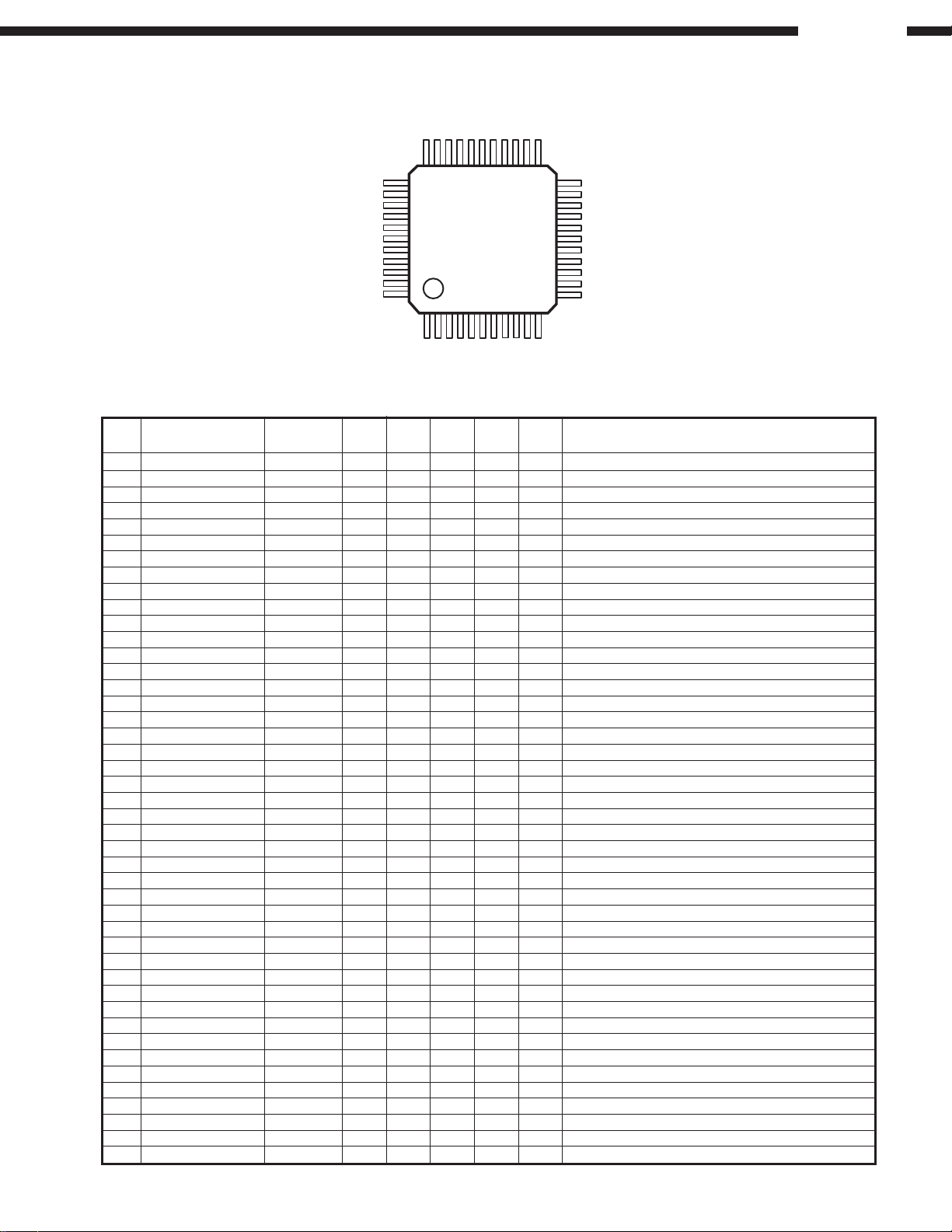
TMP86CM47U (DS: IC101, 151)
DN-D9000
33
34
23
22
TOP VIEW
44
1
11
TMP86CM47U Terminal Function
Pin
No.
1 VSS VSS — — — — — GND (0V)
2 XIN XIN I — — — — Oscillation input 8.0MHz
3 XOUT XOUT O — — — — Oscillation output
4 TEST TEST I — — — — Fixed to L
5 VDD VDD — — — — — Power (+3.3V)
6 P21(LED) DVSEL O — Pu L H Not used
7 P22 BREQ1_ O — Pu H H System µcom bus request
8 RESET_ RST_ I — — — — µcom reset
9 P20 DRLCH O — Pu H H ATAPI data register latch signal, H: Latch
10 P00(INT0) MCMD_ I — — — — System µcom serial interface
11 P01 DMA O — Pu L H ATAPI DMA mode select (H: DMA)
12 P02 DMABSY1 I — Pu — H In DMA flag (L: DMA data transfer)
13 P03 ATANS O — Pu H H System µcom serial interface
14 P04(SO) ATDATA O — Pu H H System µcom serial data receive signal
15 P05(SI) MDATA I — — — — System µcom serial data send signal
16 P06(SCK_) MCLK I — — — — System µcom serial send/receive clock
17 P07(INT4/LED) BSYIN_ I — — — H TXD BUSY input
18 P17 BSYOUT_ O — Pu H H TXD BUSY output signal (L: BUSY)
19 P16 DRES_ O — Pd L L DSP reset (L: Reset)
20 P15 DMAR_/W I/O — Pu/Pd H L/H ATAPI DMA direction select (L: Read) *
21 P14 RD_ O — — H — ATAPI read strobe
22 P13 WR_ O — — H — ATAPI write strobe
23 P12(INT2) INTRQ I Lv — — — ATAPI interrupt request signal
24 P11(INT1) DMARQ I Lv Pd — — ATAPI DMA request signal (Pd with 5.6kW)
25 P10 IORDY I — Pu — H
26 P30 D0 I/O — Pd L L ATAPI data bus 0 (APRES_ATAPI reset)
27 P31 D1 I/O — — — — ATAPI data bus 1 (CS1 device register chip select 1)
28 P32 D2 I/O — — — — ATAPI data bus 2 (CS0 device register chip select 0)
29 P33 D3 I/O — — — — ATAPI data bus 3 (DA2 device register select 2)
30 P34 D4 I/O — — — — ATAPI data bus 4 (DA1 device register select 1)
31 P35 D5 I/O — — — — ATAPI data bus 5 (DA0 device register select 0)
32 P36 D6 I/O — — — — ATAPI data bus 6
33 P37 D7 I/O — — — — ATAPI data bus 7
34 VAREF VAREF I — — — —
35 AVDD AVDD I — — — — Power (+3.3V), Power for A/D conversion circuit only
36 AVSS AVSS I — — — — GND (0V), Analog GND for A/D conversion
37 P40 D8 I/O — — — — ATAPI data bus 8
38 P41 D9 I/O — — — — ATAPI data bus 9
39 P42 D10 I/O — — — — ATAPI data bus 10
40 P43 D11 I/O — — — — ATAPI data bus 11
41 P44 D12 I/O — — — — ATAPI data bus 12
42 P45 D13 I/O — — — — ATAPI data bus 13
43 P46 D14 I/O — — — — ATAPI data bus 14
44 P47 D15 I/O — — — — ATAPI data bus 15
* Pd or Pu detected in input port when power on, Pd=CD1, Pu=CD2
Pin Name Symbol DET Ext Ini Res
12
FunctionI/O
ATAPI data transfer cycle extend request signal (Pu with 1.0kW)
GND (0V), Analog ref. V for A/D conversion, A/D not used
18
DN-D9000
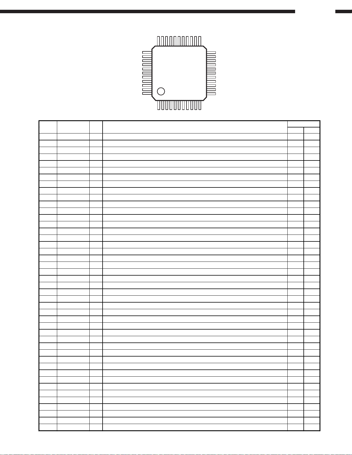
SM5902AF Terminal Function
Setting
Pin No. Symbol I/O Function
HL
1 VDD2
VDD power supply terminal.
2 UC1 IP/O Microcomputer interface extended I/O 1. Not Used (OPEN)
3 UC2 IP/O Microcomputer interface extended I/O 2. Not Used (OPEN)
4 UC3 IP/O Microcomputer interface extended I/O 3. Not Used (OPEN)
5 UC4 IP/O Microcomputer interface extended I/O 4. Not Used (OPEN)
6 UC5 IP/O Microcomputer interface extended I/O 5. Not Used (OPEN)
7 DIT O Digital audio interface terminal.
8 NTEST IP Test terminal. Test
9 CLK I 16.9344 MHz clock input.
10 Vss
Ground terminal.
11 YSRDATA I Audio serial input data.
12 YLRCK I Audio serial input LR clock. Lch Rch
13 YSCK I Audio serial input bit clock.
14 ZSCK O Audio serial output bit clock.
15 ZLRCK O Audio serial output LR clock. Lch Rch
16 ZSRDATA O Audio serial output data.
17 YFLAG I RAM overflow flag for signal processing IC. Over
18 YFCLK I X’tal system frame clock.
19 YBLKCK I Sub-code block clock signal.
20 NRESET I System reset terminal. Reset
21 ZSENSE O Microcomputer interface status output.
22 VDD1
VDD power supply terminal.
23 YDMUTE I Forcible mute terminal. Mute
24 YMLD I Microcomputer interface latch clock.
25 YMDATA I Microcomputer interface serial data.
26 YMCLK I Microcomputer interface shift clock.
27 A10 O DRAM address 10.
28 NCAS O DRAM CAS control.
29 D2 I/O DRAM data input/output 2.
30 D3 I/O DRAM data input/output 3.
31 D0 I/O DRAM data input/output 0.
32 D1 I/O DRAM data input/output 1.
33 NWE O DRAM WE control.
34 NRAS O DRAM RAS control.
35 A9 O DRAM address 9.
36 A8 O DRAM address 8.
37 A7 O DRAM address 7.
38 A6 O DRAM address 6.
39 A5 O DRAM address 5.
40 A4 O DRAM address 4.
41 A0 O DRAM address 0.
42 A1 O DRAM address 1.
43 A2 O DRAM address 2.
44 A3 O DRAM address 3.
SM5902AF (DS: IC651, 652)
33
34
23
22
TOP VIEW
44
1
11
12
19
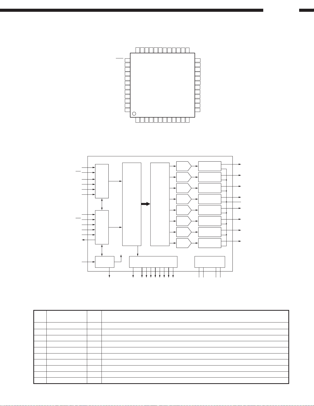
PCM1608Y (DS: IC705)
1
2
CC
MLMCMDI
MDO
ZERO8
DATA 4
ZERO7NCV
CC
V
AGND1
36 35 34 33 32 31 30 29 28 27 26 25
DN-D9000
AGND2
BCK
LRCK
DATA1 (1, 2)
DATA2 (3, 4)
DATA3 (5, 6)
DATA4 (7, 8)
TEST
RST
MC
MDI
MDO
SCKI
RST
SCKI
SCKO
BCK
LRCK
TEST
V
DGND
DATA 1
DATA 2
DATA 3
ZEROA
37
38
39
40
41
42
43
DD
TOP VIEW
44
45
46
47
48
24
23
22
21
20
19
18
17
16
15
14
13
VCC3
AGND3
CC
4
V
AGND4
OUT
8
V
AGND6
CC
5
V
AGND5
OUT
7
V
VCOM
OUT
1
V
OUT
2
V
123456789101112
6
4
5
OUT
V
OUT
V
DAC
DAC
DAC
DAC
DAC
DAC
DAC
DAC
OUT
V
3
OUT
V
Output Amp and
Low-Pass Filter
Output Amp and
Low-Pass Filter
Output Amp and
Low-Pass Filter
Output Amp and
Low-Pass Filter
Output Amp and
Low-Pass Filter
Output Amp and
Low-Pass Filter
Output Amp and
Low-Pass Filter
Output Amp and
Low-Pass Filter
Power Supply
V
OUT
1
OUT
2
V
OUT
3
V
OUT
4
V
V
COM
V
OUT
5
V
OUT
6
OUT
7
V
OUT
8
V
NC
NC
ZERO1/GPO1
ZERO3/GPO3
ZERO5/GPO5
ZERO2/GPO2
ZERO4/GPO4
ZERO6/GPO6
Serial
Input
I/F
4x/8x
Oversampling
Digital Filter
with
Function
Controller
ML
Function
Control
I/F
System Clock
Manager
System Clock
Enhanced
Multi-Level
Delta-Sigma
Modulator
Zero Detect
DD
SCKO
ZEROA
ZERO1/GPO1
ZERO2/GPO2
ZERO3/GPO3
ZERO4/GPO4
ZERO5/GPO5
ZERO6/GPO6
ZERO7
ZERO8
V
DGND
1-5
CC
V
AGND1-8
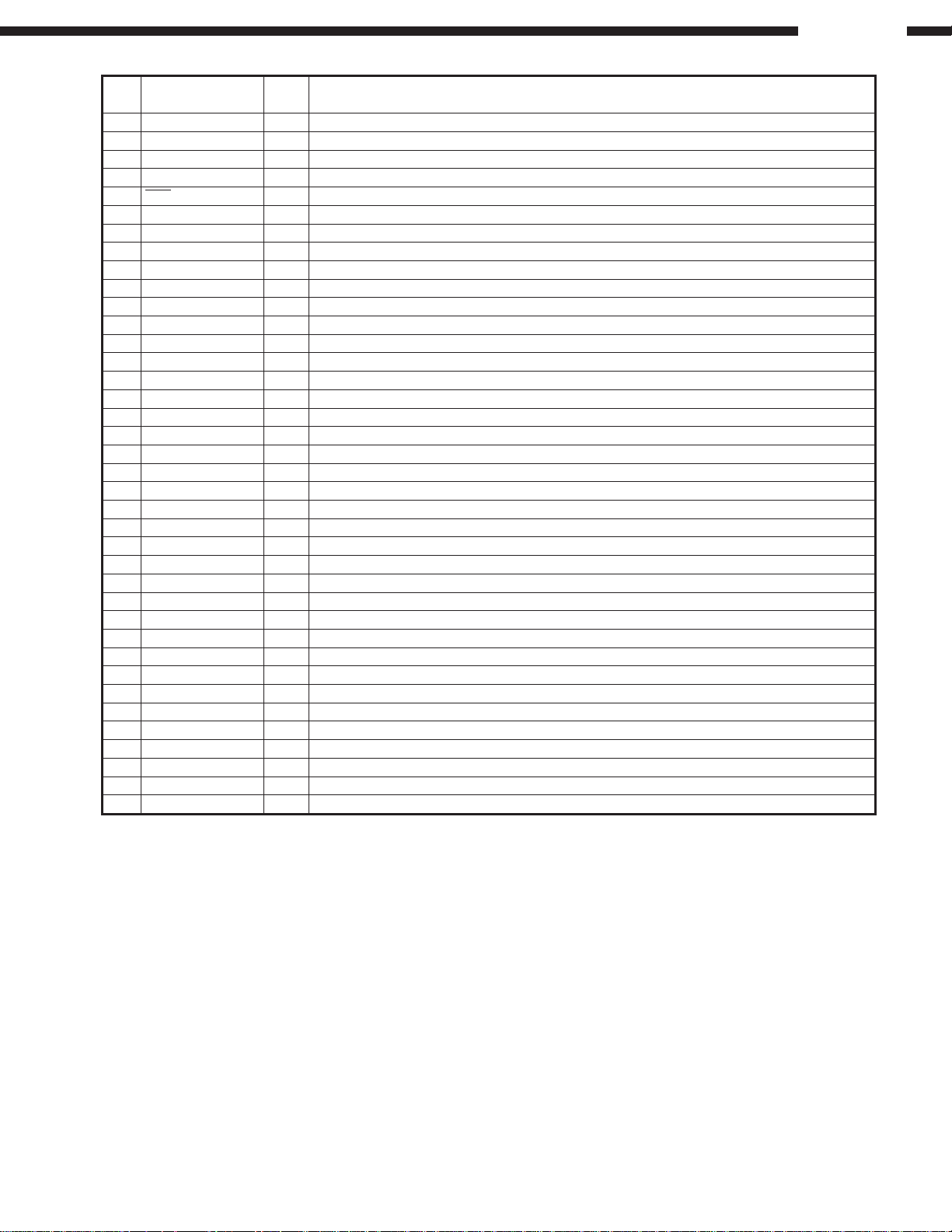
PCM1608Y Terminal Function
Pin
No.
1 ZERO1/GPO1 O Zero Data Flag for VOUT1. Can also be used as GPO pin
2 ZERO2/GPO2 O Zero Data Flag for VOUT2. Can also be used as GPO pin
3 ZERO3/GPO3 O Zero Data Flag for VOUT3. Can also be used as GPO pin
4 ZERO4/GPO4 O Zero Data Flag for VOUT4. Can also be used as GPO pin
5 ZERO5/GPO5 O Zero Data Flag for VOUT5. Can also be used as GPO pin
6 ZERO6/GPO6 O Zero Data Flag for VOUT6. Can also be used as GPO pin
7 NC — No Connection
8 NC — No Connection
9VOUT6 O Voltage Output of Audio Signal Corresponding to Rch on DATA3. Up to 96kHz
10 VOUT5 O Voltage Output of Audio Signal Corresponding to Rch on DATA3. Up to 96kHz
Pin Name
I/O
Function
20
DN-D9000
Pin
No.
Pin Name
I/O
Function
11 VOUT4 O Voltage Output of Audio Signal Corresponding to Rch on DATA2. Up to 96kHz
12 VOUT3 O Voltage Output of Audio Signal Corresponding to Rch on DATA2. Up to 96kHz
13 VOUT2 O Voltage Output of Audio Signal Corresponding to Rch on DATA1. Up to 192kHz
14 VOUT1 O Voltage Output of Audio Signal Corresponding to Rch on DATA1. Up to 192kHz
15 VCOM O Common Voltage Output. This pin should be bypassed with a 10µF capacitor to AGND
16 VOUT7 O Voltage Output for Audio Signal Corresponding to Rch on DATA4. Up to 192kHz
17 AGND5 — Analog Ground
18 VCC5 — Analog Power Supply, +5V
19 AGND6 — Analog Ground
20 VOUT8 — Voltage Output for Audio Signal Corresponding to Rch on DATA4. Up to 192kHz
21 AGND4 — Analog Ground
22 VCC4 — Analog Power Supply, +5V
23 AGND3 — Analog Ground
24 VCC3 — Analog Power Supply, +5V
25 AGND2 — Analog Ground
26 VCC2 — Analog Power Supply, +5V
27 AGND1 — Analog Ground
28 VCC1 — Analog Power Supply, +5V
29 NC — No Connection
30 ZERO7 — Zero Data Flag for VOUT7
31 DATA4 — Serial Audio Data Input VOUT7 and VOUT8
(2)
32 ZERO8 — Zero Data Flag for VOUT7
33 MDO O Serial Audio Data Output for Serial Port
34 MDI l Serial Audio Data Input for Serial Port
35 MC l Shift Clock for Serial Control Port
36 ML l Latch Enable for Serial Control Port
37 RST l System Reset, Active LOW
(1)
38 SCKI l System Clock Input frequency is 128,192,256,384,512,or 768fs.
39 SCKO O Buffered Clock Output frequency is 128,192,256,384,512,or 768fs.
40 BCK l Shift Clock Input for Serial Audio Data. Clock must be 32,48,or,64fs.
41 LRCK l Left and Right Clock Input. This clock is equal to the sampling rate, fs.
42 TEST — Test Pin. This pin should be connected to DGND.
(3)
(1)
(1)
(1)
(2)
(2)
(2)
(2)
(1)
43 VDD — Digital Power Supply, +3.3V
44 DGND — Digital Ground
45 DATA1 l Serial Audio Data Input VOUT1 and VOUT2
46 DATA2 l Serial Audio Data Input VOUT3 and VOUT4
47 DATA3 l Serial Audio Data Input VOUT5 and VOUT6
(2)
(2)
(2)
48 ZEROA O Zero Data Flag. Logical “AND” of ZERO1 through ZERO6
NOTE: (1) Schmitt-Trigger input with internal pull-down, 5V tolerant. (2) Schmitt-Trigger input, 5V tolerant. (3) Tri-state output.
21
 Loading...