

D&M Holdings lnc.
e
Copyright 2009 D&M Holdings Inc. All rights reserved.
WARNING: Violators will be prosecuted to the maximum extent possible.
s
d
Ver. 6
●
For purposes of improvement, specifications and design are subject to change without notice.
●
Please use this service manual with referring to the operating instructions without fail.
●
Some illustrations using in this service manual are slightly different from the actual set.
Please refer to the
MODIFICATION NOTICE.
SERVICE MANUAL
MODEL JP EU EC E2 EK E2A E1C EUT
AVR-4310CI
AVR-4310
MODEL JP EU EC E2 EK E2A E1C EUT
AVC-4310
33
3
AV SURROUND RECEIVER
3
AV SURROUND AMPLIFIER
S0025-1V06DM/DG0912
SAFETY PRECAUTIONS
The following check should be performed for the continued protection of the customer and service technician.
LEAKAGE CURRENT CHECK
Before returning the unit to the customer, make sure you make either (1) a leakage current check or (2) a line to chassis
resistance check. If the leakage current exceeds 0.5 milliamps, or if the resistance from chassis to either side of the
power cord is less than 460 kohms, the unit is defective.
CAUTION
Please heed the points listed below during servicing and inspection.
◎ Heed the cautions!
Spots requiring particular attention when servicing, such
as the cabinet, parts, chassis, etc., have cautions indicated
on labels or seals. Be sure to heed these cautions and the
cautions indicated in the handling instructions.
◎ Caution concerning electric shock!
(1) An AC voltage is impressed on this set, so touching in-
ternal metal parts when the set is energized could
cause electric shock. Take care to avoid electric shock,
by for example using an isolating transformer and
gloves when servicing while the set is energized, unplugging the power cord when replacing parts, etc.
(2)There are high voltage parts inside. Handle with extra
care when the set is energized.
◎ Caution concerning disassembly and
assembly!
Though great care is taken when manufacturing parts from
sheet metal, there may in some rare cases be burrs on the
edges of parts which could cause injury if fingers are
moved across them. Use gloves to protect your hands.
◎ Inspect for safety after servicing!
Check that all screws, parts and wires removed or disconnected for servicing have been put back in their original positions, inspect that no parts around the area that has been
serviced have been negatively affected, conduct an insulation check on the external metal connectors and between
the blades of the power plug, and otherwise check that
safety is ensured.
(Insulation check procedure)
Unplug the power cord from the power outlet, disconnect
the antenna, plugs, etc., and turn the power switch on. Using a 500V insulation resistance tester, check that the insulation resistance between the terminals of the power
plug and the externally exposed metal parts (antenna terminal, headphones terminal, microphone terminal, input
terminal, etc.) is 1MΩ or greater. If it is less, the set must
be inspected and repaired.
CAUTION
Concerning important safety
parts
◎ Only use designated parts!
The set's parts have specific safety properties (fire resistance, voltage resistance, etc.). For replacement parts, be
sure to use parts which have the same properties. In particular, for the important safety parts that are marked z on
wiring diagrams and parts lists, be sure to use the designated parts.
◎ Be sure to mount parts and arrange
the wires as they were originally!
For safety reasons, some parts use tape, tubes or other insulating materials, and some parts are mounted away from
the surface of printed circuit boards. Care is also taken with
the positions of the wires inside and clamps are used to
keep wires away from heating and high voltage parts, so
be sure to set everything back as it was originally.
Many of the electric and structural parts used in the set
have special safety properties. In most cases these properties are difficult to distinguish by sight, and using replacement parts with higher ratings (rated power and
withstand voltage) does not necessarily guarantee that
safety performance will be preserved. Parts with safety
properties are indicated as shown below on the wiring diagrams and parts lists is this service manual. Be sure to replace them with parts with the designated part number.
(1) Schematic diagrams ... Indicated by the z mark.
(2) Parts lists ... Indicated by the z mark.
Using parts other than the designated
parts could result in electric shock, fires or
other dangerous situations.
2
AVR-4310CI/AVR-4310/AVC-4310
DIMENSION
344
434
155
15.5
170.5
20.7
244.5
372.8
20.5
414
54.7
AVR-4310CI/AVR-4310/AVC-4310
3
AVR-4310CI/AVR-4310/AVC-4310
WIRE ARRANGEMENT
If wire bundles are untied or moved to perform adjustment or parts replacement etc., be sure to rearrange them neatly as they
were originally bundled or placed afterward.
Otherwise, incorrect arrangement can be a cause of noise generation.
Wire arrangement viewed from the top
Front Panel side
Back Panel side
4
AVR-4310CI/AVR-4310/AVC-4310
CAUTION IN SERVICING
BeforetheDigitalP.W.B.arereplaced
If you cannot specify the cause of the digital PWB defect, carry out "Initializing" → "Update to latest firmware".
The defect may be cleared.
・See the following for the method of initializing the μcom.
Initializing AV SURROUND RECEIVER
AV SURROUND RECEIVER initialization should be performed when the µcom, peripheral parts of µcom, and Digital P.W.B.
are replaced.
1. Switch off the unit.
2. Hold the following STANDARD button and DSP SIMULATION button, and switch on the unit.
3. Check that the entire display is flashing with an interval of about 1 second, and release your fingers from the 2 buttons and
the microprocessor will be initialized.
Note:・If step 3 does not work, start over from step 1.
・ All user settings will be lost and this factory setting will be recovered when this initialization mode.
So make sure to memorize your setting for restoring after the initialization.
1,2 2,3
JIG to use for servicing
When you repair the printing board, you can use the following JIG. Please order to Denon Official Service Distributor in your
region if necessary.
Extention cable kit
00D SPK- 561 EXTENSION UNIT KIT : 1 Set
00D SPK- 562 TUCP CONN. JOINT KIT : 1 Set
Extention cable for Idling Current
Parts Number for Extension Cables and Quantity of Unit.
Parts Number Parts Name Q'ty / unit Remarks
612050082004D 6P 250mm NH 1 L=250mm 6P NH Cable
612050083007D 8P 250mm NH 1 L=250mm 8P NH Cable
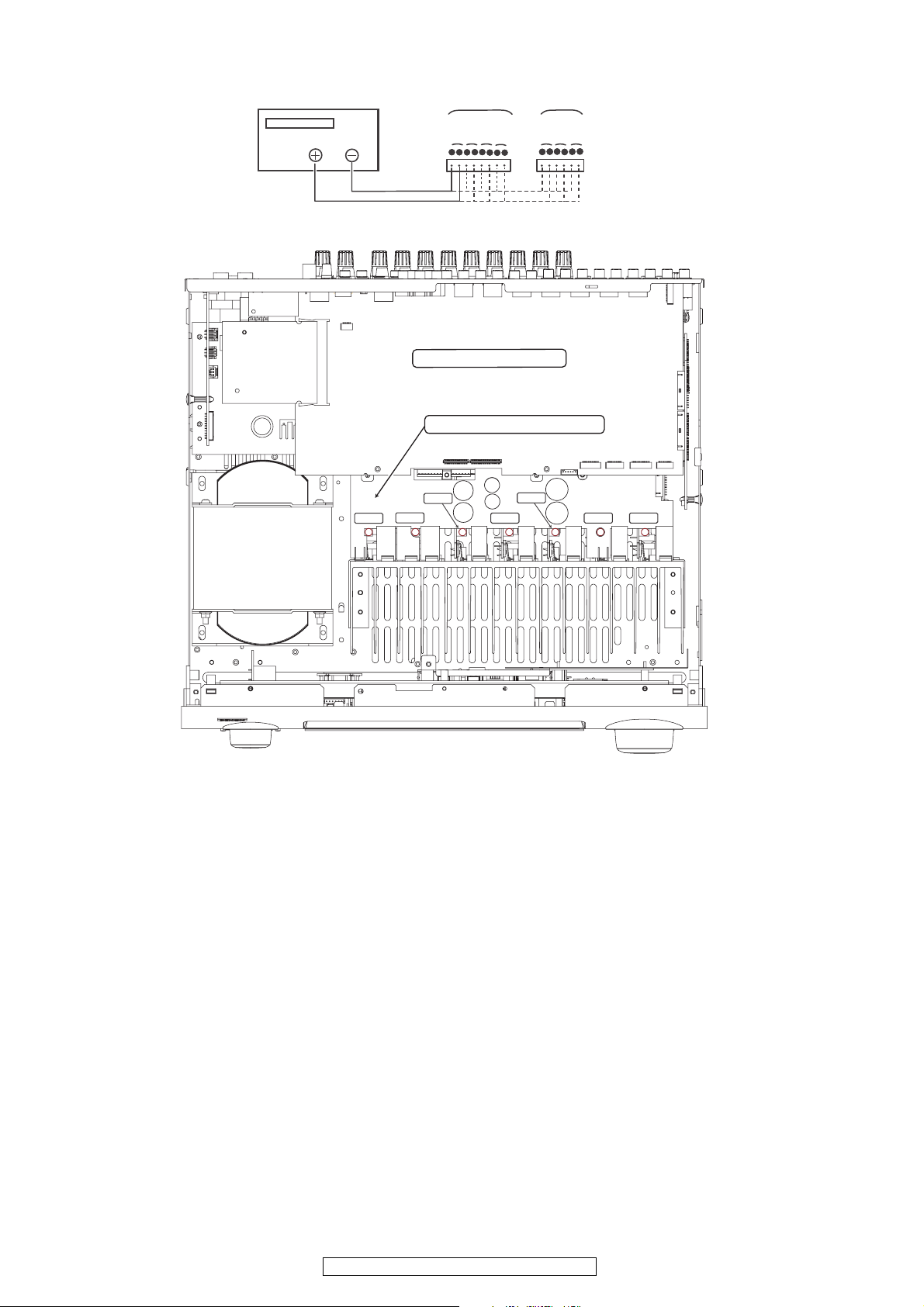
How to use and Adjust Idle Current.
1. The thin and hard plate (ex. Ruler) is fixed with the tape behind the cable.
2. The voltmeter is connected with the other side of the extension cable.
3. Refer to ADJUSTMENT(Idling Current).
5
AVR-4310CI/AVR-4310/AVC-4310
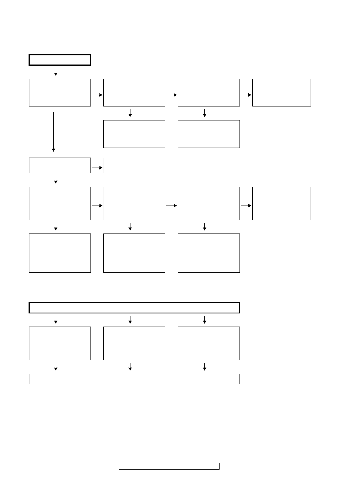
DISASSEMBLY
• Disassemble in order of the arrow of the figure of following flow.
• In the case of the re-assembling, assemble it in order of the reverse of the following flow.
• In the case of the re-assembling, observe "attention of assembling" it.
TOP COVER
BACK PANEL UNIT ASSY FRONT PANEL UNIT ASSY
Refer to "DISASSEMBLY
2. BACKPANEL UNIT ASSY" Refer to "DISASSEMBLY 1.FRONT PANEL UNIT ASSY"
DIGITAL UNIT ASSY
Refer to "DISASSEMBLY (Ref. No. of EXPLODED VIEW : B-4) (Ref. No. of EXPLODED VIEW : E-4)
3. DIGITAL UNIT ASSY" REG CONNECT-1 UNIT FRONT USB UNIT
and "EXPLODED VIEW" (Ref. No. of EXPLODED VIEW : A-15) (Ref. No. of EXPLODED VIEW : E-3)
DIGITAL UNIT CONNECT UNIT-2 MIC UNIT
(Ref. No. of EXPLODED VIEW : G) (Ref. No. of EXPLODED VIEW : D-4) (Ref. No. of EXPLODED VIEW : A-9)
REG UNIT FRONT HDMI UNIT
A.VIDEO UNIT, AUDIO UNIT AMP UNIT
and RADIATOR UNIT ASSY
Refer to "DISASSEMBLY 6. AMP UNIT" VOLUME UNIT
4. A.VIDEO UNIT, AUDIO UNIT and "EXPLODED VIEW" (Ref. No. of EXPLODED VIEW : A-4)
and RADIATOR UNIT ASSY" AMP UNIT FUNC CONNECT UNIT
and "EXPLODED VIEW" (Ref. No. of EXPLODED VIEW : D-1) (Ref. No. of EXPLODED VIEW : A-7)
A.VIDEO UNIT FUNC UNIT
(Ref. No. of EXPLODED VIEW : E-1) (Ref. No. of EXPLODED VIEW : A-6)
AUDIO UNIT
(Ref. No. of EXPLODED VIEW : E-2) Refer to "DISASSEMBLY (Ref. No. of EXPLODED VIEW : A-1)
MAIN CPU UNIT 7. P.AMP JOINT UNIT"
(Ref. No. of EXPLODED VIEW : F) and "EXPLODED VIEW"
REMOTE/IPOD UNIT P.AMP JOINT UNIT
(Ref. No. of EXPLODED VIEW : B-5) (Ref. No. of EXPLODED VIEW : D-2)
232C UNIT
(Ref. No. of EXPLODED VIEW : B-6)
REG UNIT
5. REG UNIT" P.SW UNIT
and "EXPLODED VIEW" (Ref. No. of EXPLODED VIEW : A-8)
FRONT IN UNIT
(Ref. No. of EXPLODED VIEW : A-10)
VR CONNECT UNIT
Refer to "DISASSEMBLY (Ref. No. of EXPLODED VIEW : A-5)
P.AMP JOINT UNIT
FLD UNIT
P.AMP UNIT
Refer to "DISASSEMBLY
9.P.AMP UNIT"
and "EXPLODED VIEW"
P.AMP UNIT
(Ref. No. of EXPLODED VIEW : D-1〜7)
Refer to "DISASSEMBLY
6
AVR-4310CI/AVR-4310/AVC-4310
About the photos used for descriptions in the “DISASSEMBLY” section.
• The direction from which the photographs used herein were photographed is indicated at "Direction of photograph: ***" at
the left of the respective photographs.
• Refer to the table below for a description of the direction in which the photos were taken.
• Photographs for which no direction is indicated were taken from above the product.
The viewpoint of each photograph
(Photografy direction)
[View from above]
Direction of photograph: C
Direction of photograph: B
Front side
Direction of photograph: D
Direction of photograph: A
1. FRONT PANEL UNIT ASSY
Proceeding : TOP COVER →
(1) Remove the screws.
View from bottom
(2) Cut the wire clampers then disconnect the connector wires.
CX021
Direction of photograph: D
FRONT PANEL UNIT ASSY
cut
cut
CY062
cut
7
AVR-4310CI/AVR-4310/AVC-4310
(3) Remove the FFC cover and acetate tapes. Disconnect the FFC Cables.
FFC Cable
FFC Cable
Direction of photograph: C
Acetate tape
(4) Remove the screws.
ٟ
Please refer to "EXPLODED VIEW" for the disassembly method of each P.W.B included in FRONT PANEL ASSY.
FFC Cover
[Attention of assembling]
When mounting the FRONT PANEL ASSY on the CHASSIS, do so with the DOOR open so as to prevent
breaking the EARTH PLATE(DOOR).
If the FRONT PANEL ASSY is mounted on the chassis with the DOOR closed, the EARTH PLATE(DOOR) will
hit the CHASSIS and break.
DOOR open
EARTH PLATE (DOOR)
Direction of photograph: A
DOOR closed (EARTH PLATE (DOOR) will be broken.)
EARTH PLATE (DOOR)
Direction of photograph: A
DOOR
DOOR
8
AVR-4310CI/AVR-4310/AVC-4310
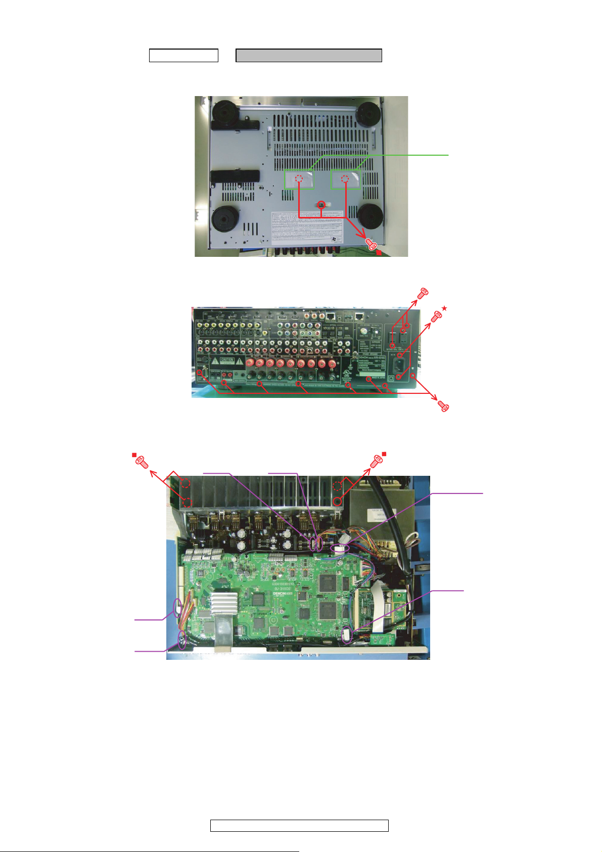
2. BACK PANEL UNIT ASSY
Proceeding : TOP COVER → BACK PANEL UNIT ASSY
(1) Remove the Sheets, then remove the screws.
View from bottom
Sheets
(2) Remove the screws.
Direction of photograph: A
(3) Disconnect the connector wires and FFC Cable, then remove the screws.
CX055
CX074
ً
ً
FFC Cable
CY101
CY153
CY052
9
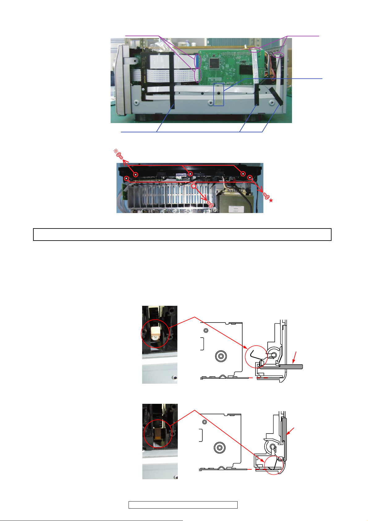
AVR-4310CI/AVR-4310/AVC-4310
(4) Remove the FFC cover, PWB HOLDER and acetate tapes. Cut the wire clamper, then disconnect the connector wire
and FFC Cable.
FFC Cable
CX068
Direction of photograph: C
cut
Acetate tape
(5) Cut the wire clamper, then disconnect the connector wire.
BACK PANEL UNIT ASSY
PWB HOLDER
v
FFC Cover
Direction of photograph: D
Acetate tape
CX091
cut
10
AVR-4310CI/AVR-4310/AVC-4310
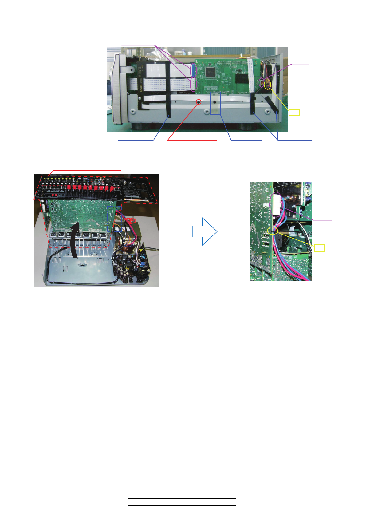
3. DIGITAL UNIT ASSY
Proceeding : TOP COVER →
(1) Remove the alminium tape, then cut the wire clampers. Disconnect the connector wire, FFC Cables, and board to
board.
BACK PANEL UNIT ASSY
→
DIGITAL UNIT ASSY
MAIN CPU UNIT
Board to board
CX124
(2) Remove the screws.
FFC Cable
CX058
ً
cut
FFC Cable
Alminium Tape
CX047
cut
DIGTAL UNIT ASSY
FFC Cable
CY124
CY061
◆
Direction of photograph: A
11
AVR-4310CI/AVR-4310/AVC-4310
4. A.VIDEO UNIT, AUDIO UNIT and RADIATOR UNIT ASSY
Proceeding : TOP COVER →
→
A.VIDEO UNIT, AUDIO UNIT and RADIATOR UNIT ASSY
(1) Disconnect the board to board.
Direction of photograph: C
v
(2) Disconnect the connector wires.
BACK PANEL UNIT ASSY
CX073CX192
→
MAIN CPU UNIT
DIGITAL UNIT ASSY
(3) Remove the screws.
Direction of photograph: A
A.VIDEO UNIT
AUDIO UNIT
RADIATOR UNIT ASSY
12
AVR-4310CI/AVR-4310/AVC-4310
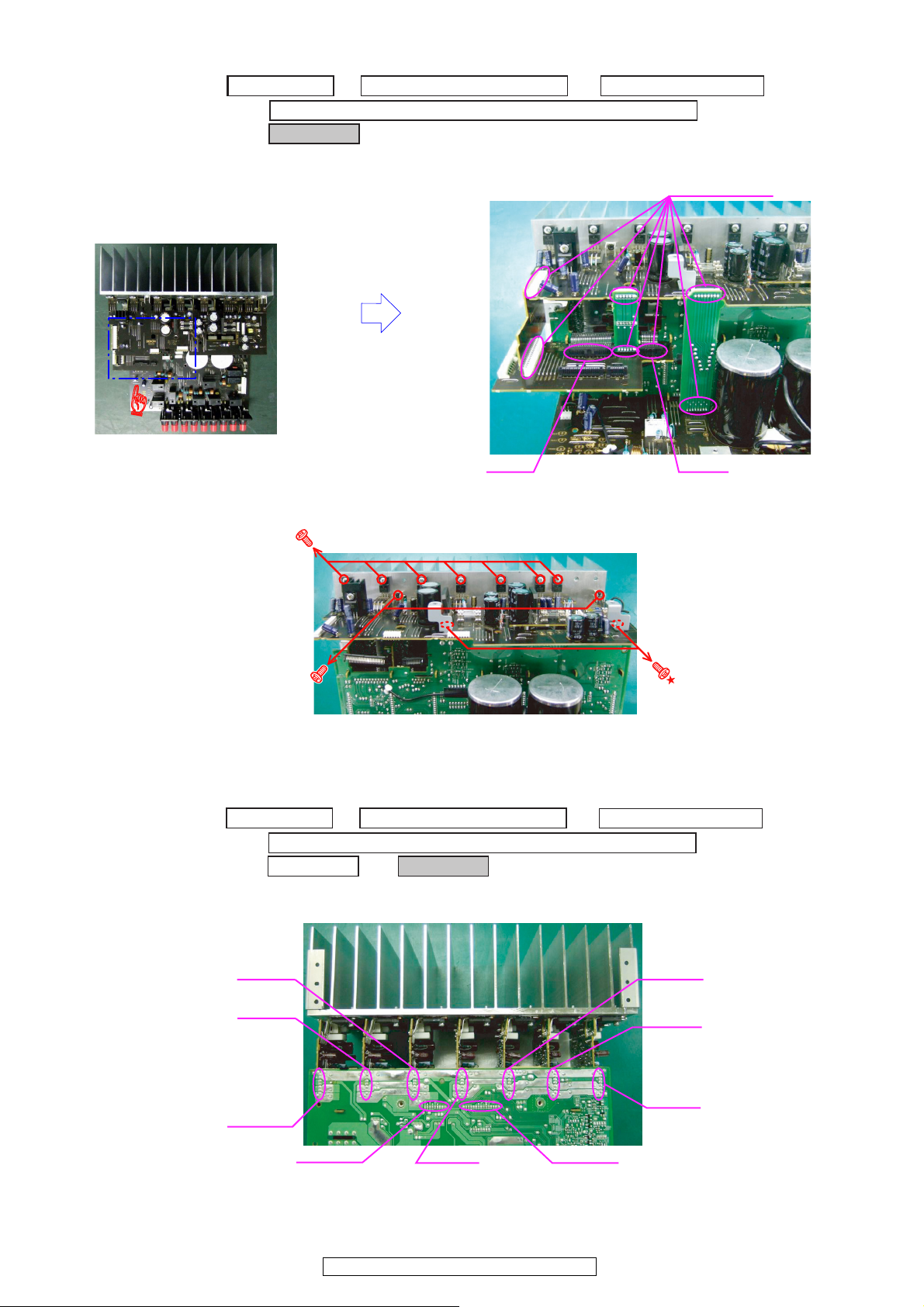
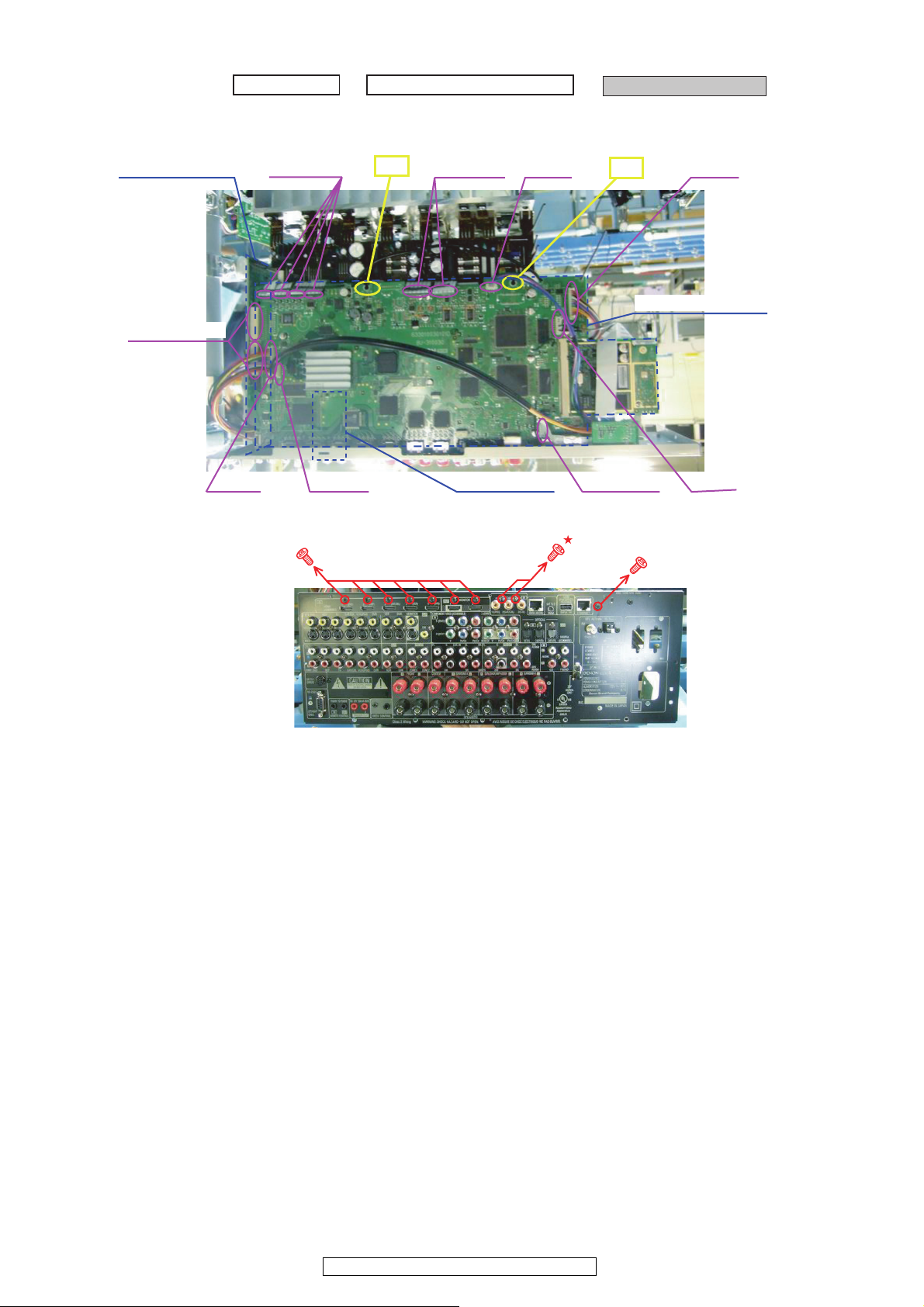
5. REG UNIT
Proceeding : TOP COVER →
→
A.VIDEO UNIT, AUDIO UNIT and RADIATOR UNIT ASSY
→
REG UNIT
(1) Disconnect the board to board and connector wires.
BACK PANEL UNIT ASSY
v
→
DIGITAL UNIT ASSY
Board to board
Direction of photograph: A
(2) Disconnect the connector wires, then remove the screws.
ً
Direction of photograph: A
ٟ
6. AMP UNIT
Proceeding : TOP COVER →
→
A.VIDEO UNIT, AUDIO UNIT and RADIATOR UNIT ASSY
→→
REG UNIT AMP UNIT
(1) Disconnect the VH connector and conector.
BACK PANEL UNIT ASSY
CX231
→
DIGITAL UNIT ASSY
CX092
CX871
CX874
View from bottom
CX876
CX873
CX851CX891
13
AVR-4310CI/AVR-4310/AVC-4310
CX872
CX875
CX877
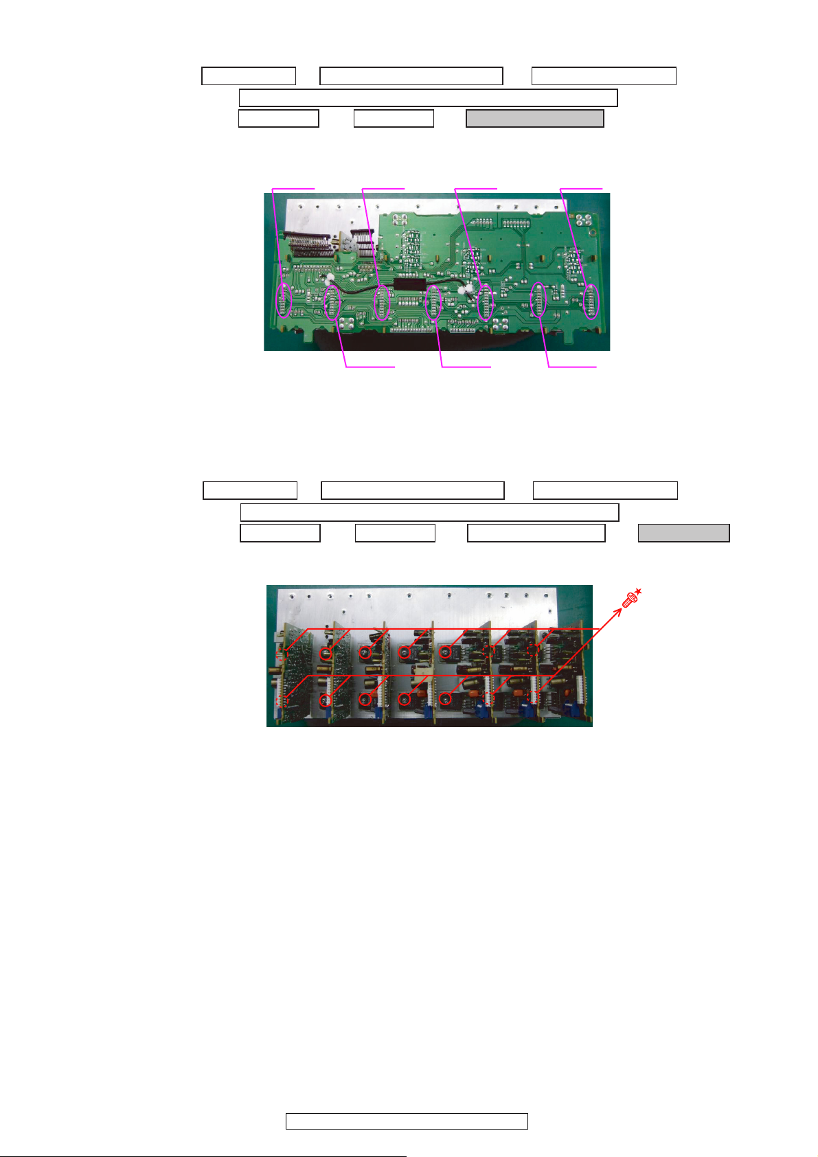
7. P.AMP JOINT UNIT
Proceeding : TOP COVER →
→
A.VIDEO UNIT, AUDIO UNIT and RADIATOR UNIT ASSY
→→→
REG UNIT AMP UNIT P.AMP JOINT UNIT
(1) Disconnect the connector.
Direction of photograph: A
BACK PANEL UNIT ASSY
→
DIGITAL UNIT ASSY
CX806CX811CX812CX807
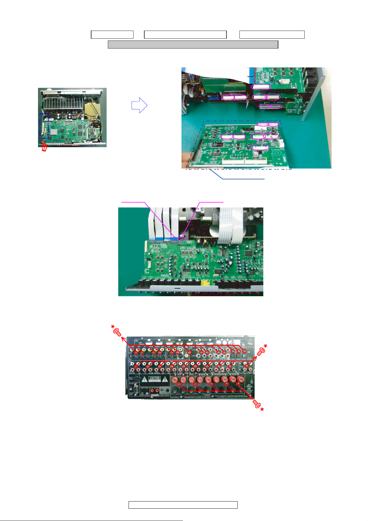
8. P.AMP UNIT
Proceeding : TOP COVER →
→
A.VIDEO UNIT, AUDIO UNIT and RADIATOR UNIT ASSY
→→→
REG UNIT AMP UNIT P.AMP JOINT UNIT P.AMP UNIT
(1) Remove the screws.
Direction of photograph: B
CX803CX805
BACK PANEL UNIT ASSY
CX804
→
DIGITAL UNIT ASSY
→
14
AVR-4310CI/AVR-4310/AVC-4310
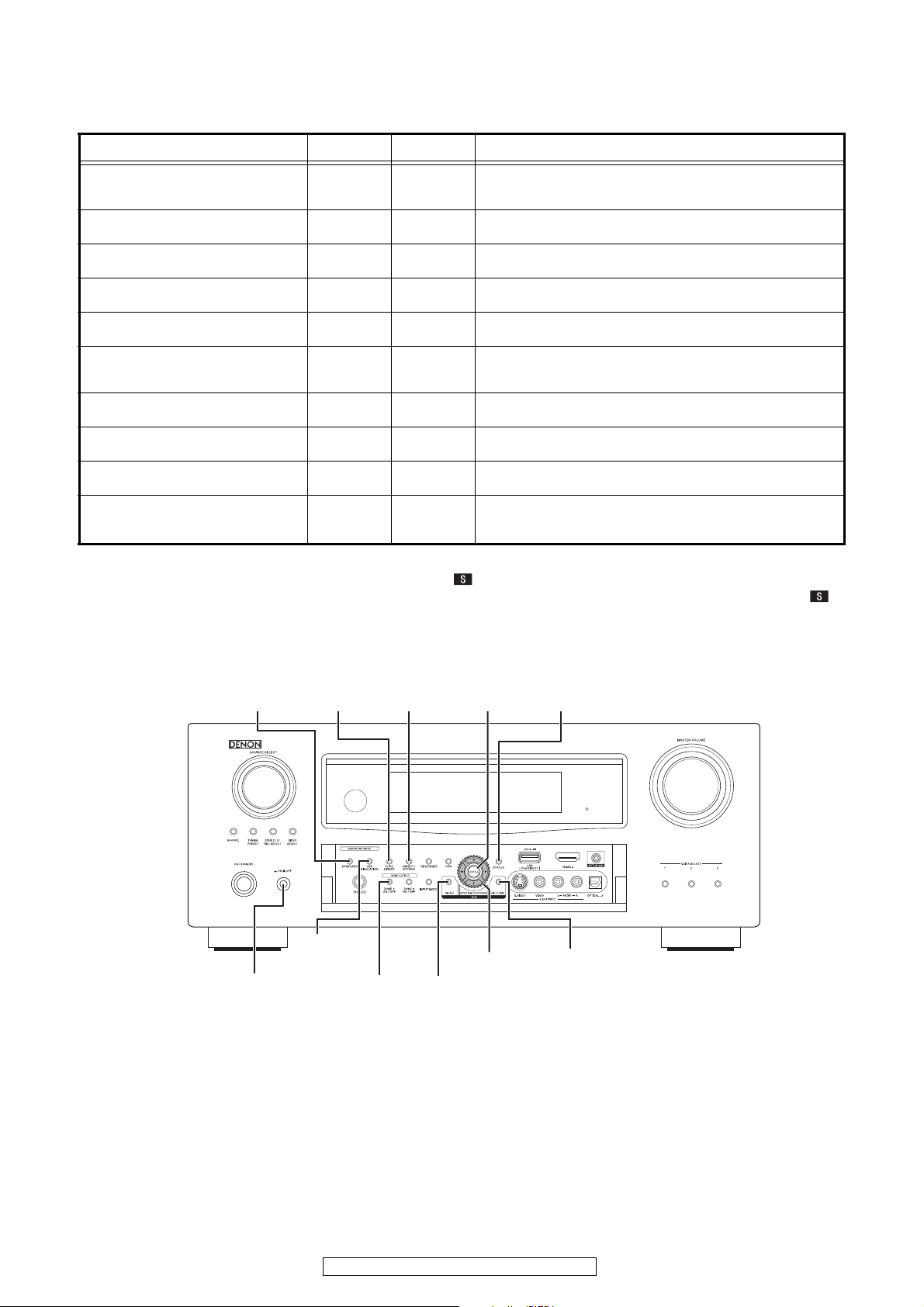
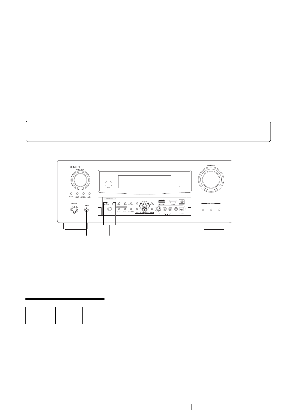
SPECIAL MODE
ON/OFF
RETURN
ZONE2
DSP
SIMULATION
STANDARD STATUSENTER
PURE
DIRECT
DIRECT/
STEREO
MENU
CURSOR
Special mode setting button
※ Press the ON/OFF button to turn on while pressing both buttons A and B at the same time.
Mode Button A Button B contents
Version display
(µcom/DSP Error Display)
Displaying the protection history mode
Initialization mode
(Remove settings for Installer Setup.)
Initialization mode
(Includes settings for Installer Setup)
Mode for switching tuner frequency step
Mode for preventing remote control
acceptance
Panel lock mode
Panel lock mode
(Remove Master volume)
Cancellation of panel lock mode
Installer Setup mode*1
STATUS RETURN
STATUS MENU
STANDARD
CURSOR UP
STANDARD
STATUS ENTER
DSP
SIMULATION
DIRECT/
STEREO
PURE
DIRECT
MENU
SIMULATION
CURSOR
DOWN
DIRECT/
STEREO
ZONE2
ZONE2
ZONE2
CURSOR
LEFT
DSP
Serial No. and firmware versions such as Main, Sub, DSP are
displayed in the FL manager. Errors are displayed when they
occur. (Refer to 16 page.)
Displaying the protection history
(Refer to 18 page.)
Backup data initialization is carried out.
(Remove settings for Installer Setup.)
Backup data initialization is carried out.
(Includes settings for Installer Setup)
---E2 model only--Change tuner frequency step to FM:200kHz/AM:10kHzSTEP. g
Operations using remote control are rejected.
(Mode cancellation: Turn off power and execute the same button
operations as when performing setup.)
Operations using main unit panel buttons or master volume are
rejected.
Operations using main unit panel buttons are rejected.
Panel lock mode is cancelled.
Access Remote Maintenance mode via the internet.Installer Setup
is displayed on GUI/Option Menu.
Refer to AVR4310_RemoteMaintenance_.pdf of SDI.
*1 : About RS-232C communications
RS-232C communications are not possible when" " is displayed on the FL display.
Press and hold in the "STATUS" and " ▽ " buttons for over 3 seconds with the power turned on to turn the " "
display off. RS-232C communications are now enabled.
AVR-4310CI/AVR-4310/AVC-4310
15
1. Version display (µcom/DSP Error Display)
S
er ial No. AVR
9
041500001
Ma i n : .
Ma i n ROM : .
Ma i n FBL : .
Sub : .
DSP1 : .
DSP2 : .
A
ud i o PLD : .
V
ideo PLD : .
G
UI Conf ig:
G
UI PRG:
G
UI DAT:
E
ther FBL
-
E
ther SBL
-
E
ther IMG
-
*
Ethernet MAC
-
*
HDSDK : .
*
HDDSP : C0 0 0 2 . 0 0 0
*
Mu l t EQ P r o APP
...
*
Mu l t EQ P r o I CL
...
1. Version display (µcom/DSP Error Display)
1.1. Operation Spec
1.1. Operation Spec
µcom version display mode:
µcom version display mode:
When the following conditions are satisfied at its starting state, error information is displayed before version information.
When the following conditions are satisfied at its starting state, error information is displayed before version information.
Starting method (same as µcom version display):
Starting method (same as µcom version display):
Press the ON/OFF button to turn on while pressing both buttons STATUS and RETURN at the same time.
Press the ON/OFF button to turn on while pressing both buttons STATUS and RETURN at the same time.
("Error information" is displayed after about 10 seconds.)
("Error information" is displayed after about 10 seconds.)
The FL display changes in the order given in item-1.2. each time you press the STATUS button.
The FL display changes in the order given in item-1.2. each time you press the STATUS button.
1.2. Display Order
1.2. Display Order
Error information(Refer to 1.3. Error display) → qModel destination information wMain-µcom version information
Error information(Refer to 1.3. Error display) qModel destination information wMain-µcom version information
eMain1st Boot Loader rDSP1version information tAudio PLD yGUI FPGA Config uGUI Nios Program
eMain1st Boot Loader rDSP1version information tAudio PLD yGUI FPGA Config uGUI Nios Program
iETHER(DM860) First BootLoafer, HardwareID oETHER(DM860) Second BootLoafer, RhapsodyFlag
iETHER(DM860) First BootLoafer, HardwareID oETHER(DM860) Second BootLoafer, RhapsodyFlag
Q0ETHER(DM860) IMAGE Q1ETHER(DM850) MAC ADDRESS information
Q0ETHER(DM860) IMAGE Q1ETHER(DM850) MAC ADDRESS information
(E2 model only)
Q2HD RADIO SDK /HD RADIO DSP
Q2HD RADIO SDK /HD RADIO DSP
Q4MultEQ Pro ICL (Displayed when Audyssey Pro is complete)
Q4MultEQ Pro ICL (Displayed when Audyssey Pro is complete)
No. Display item Display
q
Model destination
Cereal No.
(E2 model only)
Q3MultEQ Pro APP (Displayed when Audyssey Pro is complete)
Q3MultEQ Pro APP (Displayed when Audyssey Pro is complete)
w
e
r
t
y
u
i
o
Main-µcom
MainFLASH
Main 1st Boot Loder
Sub-µcom
Audio PLD
Video PLD
GUI FPGA
GUI Sflash Nios
GUI Sflash Font
DM860 1st Bootloader
- Hard ID
DM860 2nd Bootloader
- Rhapsody Flag
DSP 1
DSP 2
Q0
Q1
Q2
Q3
Q4
DM860 Image
ETHER MAC ADDRESS
HD RADIO SDK
HD RADIO DSP
MultEQ Pro APP
MultEQ Pro ICL
16
AVR-4310CI/AVR-4310/AVC-4310
1.3. Error display
P
ROT EC T H I STORY
:
NO PROTEC T
P
ROT EC T H I STORY
:
ASO / DC
P
ROT EC T H I STORY
:
THERMAL
See the following table for each "Error information" display and its contents (status). Display order is ①②③④⑤⑥ .
Condition State Display
①
Sub-µcom
NG
② DIR NG
③ DSP1 NG
④ DSP2 NG
⑤ EEPROM NG
⑥
Both SUB/DSP
/EEPROM OK
No response from Sub-µcom
No response from DIR
When DSP boot, executing DSP reset makes no change to DSP1 FLAGO port "H".
No change to DSP1 FLAGO port "H" before issuing DSP command.
When DSP data read, executing WRITE="L" makes no change to ACK="H".
When DSP data read, executing REQ="L" makes no change to ACK="L".
When DSP data write, executing WRITE="H" makes no change to ACK="H".
When DSP data write, executing REQ="L" makes no change to ACK="L".
When DSP special code boot, executing DSP reset makes no change to DSP1
FLAGO port "H".
No change to DSP1 FLAGO port "H" before issuing DSP special read command.
No change to DSP1 FLAGO port "H" before DSP version read.
When DSP boot, executing DSP reset makes no change to DSP2 FLAGO port "H".
No change to DSP2 FLAGO port "H" before issuing DSP command.
When DSP data read, executing WRITE="L" makes no change to ACK="H".
When DSP data read, executing REQ="L" makes no change to ACK="L".
When DSP data write, executing WRITE="H" makes no change to ACK="H".
When DSP data write, executing REQ="L" makes no change to ACK="L".
When DSP special code boot, executing DSP reset makes no change to DSP2
FLAGO port "H".
No change to DSP2 FLAGO port "H" before issuing DSP special read command.
No change to DSP2 FLAGO port "H" before DSP version read.
Error appeared in EEPROM checksum.(*** is a block address number.)
"□SUB□ □ERROR□01□□"
"□DIR□ □ERROR□01□□"
"□ DSP1 □ERROR □01□ □"
"□ DSP1 □ERROR □02□ □"
"□ DSP1 □ERROR □03□ □"
"□ DSP1 □ERROR □04□ □"
"□ DSP1 □ERROR □05□ □"
"□ DSP1 □ERROR □06□ □"
"□ DSP1 □ERROR □11□ □"
"□ DSP1 □ERROR □12□ □"
"□ DSP1 □ERROR □13□ □"
"□ DSP2 □ERROR □01□ □"
"□ DSP2 □ERROR □02□□ "
"□ DSP2 □ERROR □03□ □"
"□ DSP2 □ERROR □04□ □"
"□ DSP2 □ERROR □05□ □"
"□ DSP2 □ERROR □06□ □"
"□ DSP2 □ERROR □11□ □"
"□ DSP2 □ERROR □12□ □"
"□ DSP2 □ERROR □13□ □"
"□E2PROM□ERR***□ □"
(No error display, version display only)
2. Displaying the protection history mode
2.1. Operation specifications
ERROR MODE(displaying the protection history)
When started up, the error information is displayed.
Starting up:
With the "MENU" and "STATUS" buttons pressed, press the "ON/OFF" button to turn the power on. The error (protection
history display) mode is set.
Then, press the "STATUS" button to turn on the FL display.
2.2. About the display on the FL display
When the "STATUS" button is pressed after setting the error (protection history display) mode, a history like the one shown
below is displayed, depending on the conditions.
(1) Normally (when there has been no protection incident)
(2) For ASO/DC (when the last protection incident was ASO or DC protection)
(3) For THERMAL (when the last protection incident was THERMAL protection)
When the "STATUS" button is pressed again after the above protection history is displayed, the normal display reappears.
17
AVR-4310CI/AVR-4310/AVC-4310
2.3. Clearing the protection history
P
ROT EC T H I STORY
:
THERMAL
P
ROT EC T H I STORY
CLEAR
P
ROT EC T H I STORY
:
NO PROTEC T
*
Tune r FRQ Se t
0
MA9/FM50M
1
*
Tune r FRQ Se t
0
MA10/FM20
1
There are two ways to clear the protection history, as described below.
(1) Start up the error (protection history display) mode, display the error, then press and hold in the "ENTER" button for 3
seconds.
Press and hold in the "ENTER" button for 3 seconds
The above is displayed and the protection history is cleared.
(2) Initialize.
※ If you want to save a backup, use the method in 3.(1) above.
Warning indication by the STANDBY LED
If the power is turned off when a protection incident has been detected, the STANDBY LED (red) flashes as follows as
warning according to the conditions in which the protection incident occurred.
(1) ASO/DC PROTECTION : Flashes in cycles of 0.5 seconds (0.25 seconds lit, 0.25 seconds off)
(2) THERMAL PROTECTION : Flashes in cycles of 2 seconds (1 second lit, 1 second off)
3. Mode for switching tuner frequency step ---E2 model only--- g
3.1. Operation specifications
Change tuner frequency step to FM:200kHz/AM:10kHz STEP.
Starting up:
(1) With the "STANDARD" and "DIRECT/STEREO" buttons pressed, press the "ON/OFF" button to turn the power on.
"*Tuner FRQ Set" appears on the display.
(2) Use 0 1 and select "<AM10/FM200>".
(3) Press the "ENTER" button.
(4) Press the "ON/OFF" button to turn the power off.
(5) Then, press the "ON/OFF" button to turn the power on.
NOTE : Backup data(Remove settings for Installer Setup) initialization is carried out automatically.
18
AVR-4310CI/AVR-4310/AVC-4310
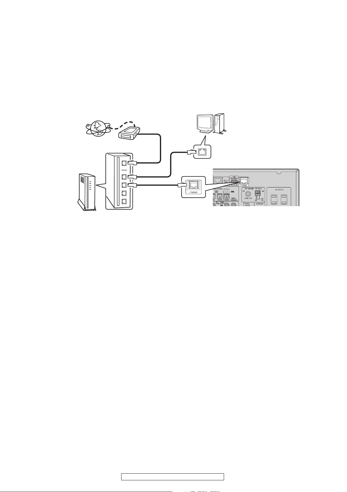
VERSION UPGRADE PROCEDURE OF FIRMWARE
You can update by downloading the latest firmware from the Internet.
1.Update from the Internet
1.1. Connecting to the Network
(1) System Requirement
• Internet Connection by Broadband Circuit
• Modem
• Router
• Ethernet cable (CAT-5 or greater recommended)
(2) Setting
Internet
Computer
Router
Modem
To WAN port
To LAN port
To LAN port
ETHERNET
connector
LAN port/
Ethernet
connector
1.2. Check for Update and Update
Check if the latest firmware exists. You can also check approximately how long it will take to complete an update.
(1) Press the MENU button on the remote control to display the GUI menu.
(2) Use the cursor buttons to select "Manual Setup" → "Option Setup" → "Firmware Update" → "Update Check".
(3) Press the ENTER buttom.
• The latest version of the firmware uploaded to the web is displayed.
• If the latest firmware version is on the web, proceed to (4).
• If the latest firmware is already installed, press the MENU button to close the menu.
(4) Use the cursor buttons to select "Update", then press the ENTER button.
• During update, the power indicator lights red and the GUI screen is shut down. And a rough remaining time is
indicated on the display.
• When updating is complete the power indicator lights green and normal status is resumed.
(5) Press the MENU button to close the menu.
--- Cautions on Firmware Update ---
• In order to use these functions, you must have the correct system requirements and settings for a broadband Internet
connection.
• Do not turn off the power until updating is completed.
Even with a broadband connection to the Internet, approximately about 1 hour is required for the updating procedure to
be completed.
Once updating starts, normal operations on the AVR-4310 cannot be performed until updating is completed. Also, setting
items of the GUI menu of AVR-4310 or setting items of the image adjustment may be initialized.
Make a note of the settings before updating, and set them again after updating.
19
AVR-4310CI/AVR-4310/AVC-4310
1.3. About the error code
See the chart below for error codes, details of faults, and coping strategies when firmware updates are performed
through DPMS (Denon Product Management Server).
Error
code
01 Log-in to DPMS has failed.
02
03 Connection to DPMS failed.
04
05
06
Details of Error code Display Coping strategies
Line, etc., is busy when logging
into DPMS.
Firmware file data was requested
but error message was received.
Firmware file data was requested
but it timed out.
Firmware file data was requested
but error message was received.
og i n f a i l ed
L
erver is busy
S
onnec t i on f a i l
C
onnec t i on f a i l
C
onnec t i on f a i l
C
onnec t i on f a i l
C
Reset and update again.
Carry out the update in an environment
that has little network load.
01
Carry out the update in an environment
that has little network load.
02
Check the network connection.
Carry out the update in an environment
that has little network load.
03
Check the network connection.
Carry out the update in an environment
that has little network load.
04
Check the network connection.
Carry out the update in an environment
that has little network load.
05
Check the network connection.
Carry out the update in an environment
that has little network load.
06
All firmware file data was
07
requested but it timed out.
Main CPU firmware file data was
08
requested but error message was
received.
Main CPU firmware file data was
09
requested but it timed out.
Error (NG) message received
when downloading Main CPU firm-
0A
ware.
Error (line congestion) message
0B
received when downloading Main
CPU firmware.
Error (connection failure) mes-
0C
sage received when downloading
Main CPU firmware.
Data acquisition failed (timed out)
0D
when downloading Main CPU firmware.
onnec t i on f a i l
C
onnec t i on f a i l
C
onnec t i on f a i l
C
own l o ad f a i l
D
own l o ad f a i l
D
own l o ad f a i l
D
onnec t i on f a i l
C
Check the network connection.
Carry out the update in an environment
that has little network load.
07
Check the network connection.
Carry out the update in an environment
that has little network load.
08
Check the network connection.
Carry out the update in an environment
that has little network load.
09
Turn the power off then back on.
Updating starts automatically.
Carry out the update in an environment
0A
that has little network load.
Turn the power off then back on.
Updating starts automatically.
Carry out the update in an environment
0B
that has little network load.
Turn the power off then back on.
Updating starts automatically.
Carry out the update in an environment
0C
that has little network load.
Turn the power off then back on.
Updating starts automatically.
Carry out the update in an environment
0D
that has little network load.
Main CPU failed to receive firm-
30
ware for rewriting sent from
DM860 (when timed out).
ain F i r m
M
pda t i ng fa i l 30
U
***
mi n
20
AVR-4310CI/AVR-4310/AVC-4310
Turn the power off then back on.
Updating starts automatically.

Error
code
Details of Error code Display Coping strategies
Main CPU failed to receive firm-
31
ware for rewriting sent from
DM860 (when an error )
There was invalid data in the firmware for rewriting sent from
32
DM860 to Main CPU (when a
Check Sum error).
The deletion of block data failed
33
before rewriting Main CPU.
The rewriting of block data failed
34
when rewriting Main CPU.
The data verification was invalid
35
after rewriting Main CPU.
Log-in to DPMS has failed when
36
rewriting firmware such as Sub
CPU, DSP, FPGA, and PLD.
Line, etc., is busy when logging
into DPMS when rewriting firm-
37
ware such as Sub CPU, DSP,
FPGA, and PLD.
ain Fi rm
M
pda t i ng fa i l 31
U
ain
M
pda t i ng fa i l 32
U
ain
M
rase fai l 33
E
ain
M
pda t i ng fa i l 34
U
ain
M
pda t eCheckNG 35
U
og i n f a i l ed
L
erver is busy
S
Firm
Firm
Firm
***
***
***
***
***
mi n
mi n
mi n
mi n
mi n
Turn the power off then back on.
Updating starts automatically.
Turn the power off then back on.
Updating starts automatically.
Turn the power off then back on.
Updating starts automatically.
Turn the power off then back on.
Updating starts automatically.
Turn the power off then back on.
Updating starts automatically.
Carry out the update in an environment
that has little network load.
36
Carry out the update in an environment
that has little network load.
37
Connection to DPMS failed when
38
rewriting firmware such as Sub
CPU, DSP, FPGA, and PLD.
Connection to DPMS timed out
39
when rewriting firmware such as
Sub CPU, DSP, FPGA, and PLD.
Error (NG) message received
3A
when downloading firmware when
rewriting Main CPU.
Error (line congestion) message
3B
received when downloading firmware when rewriting Main CPU.
Error (connection failure) message received when downloading
3C
firmware when rewriting Main
CPU.
Data acquisition failed (timed out)
3D
when downloading firmware when
rewriting Main CPU.
Error message received regarding
3E
firmware data when rewriting Main
CPU.
onnec t i on f a i l
C
onnec t i on f a i l
C
own l o ad f a i l
D
own l o ad f a i l
D
own l o ad f a i l
D
onnec t i on f a i l
C
onnec t i on f a i l
C
Check the network connection.
Carry out the update in an environment
that has little network load.
38
Check the network connection.
Carry out the update in an environment
that has little network load.
39
Turn the power off then back on.
Updating starts automatically.
Carry out the update in an environment
3A
that has little network load.
Turn the power off then back on.
Updating starts automatically.
Carry out the update in an environment
3B
that has little network load.
Turn the power off then back on.
Updating starts automatically.
Carry out the update in an environment
3C
that has little network load.
Turn the power off then back on.
Updating starts automatically.
Carry out the update in an environment
3D
that has little network load.
Check the network connection.
Carry out the update in an environment
that has little network load.
3E
Firmware file data was requested
3F
but it timed out when rewriting
Main CPU.
onnec t i on f a i l
C
21
AVR-4310CI/AVR-4310/AVC-4310
Check the network connection.
Carry out the update in an environment
that has little network load.
3F
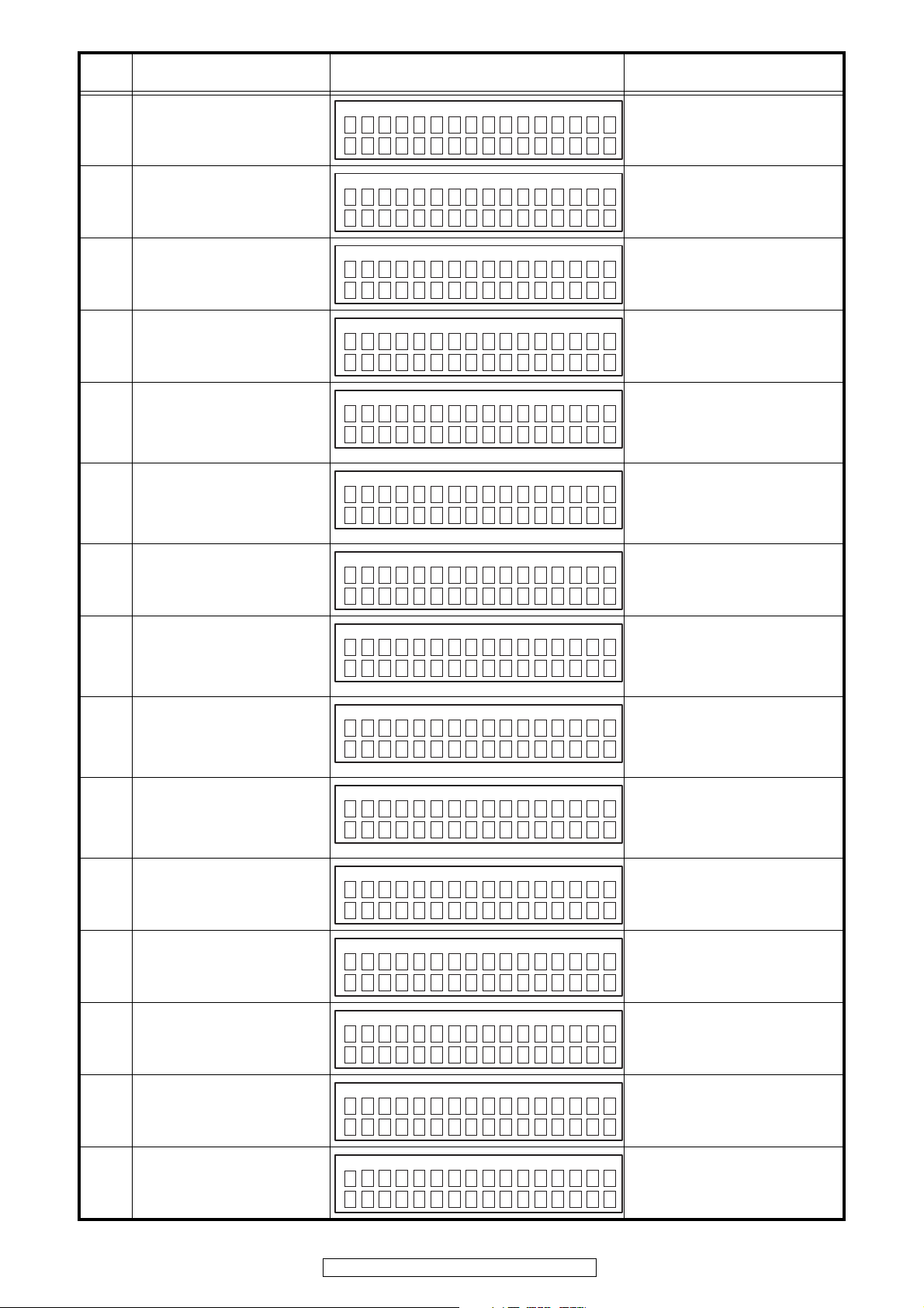
Error
code
Details of Error code Display Coping strategies
Log-in to DPMS has failed when
50
rewriting firmware such as Sub
CPU, DSP, FPGA, and PLD.
Line, etc., is busy when logging
into DPMS when rewriting firm-
51
ware such as Sub CPU, DSP,
FPGA, and PLD.
Connection to DPMS failed when
52
rewriting firmware such as Sub
CPU, DSP, FPGA, and PLD.
Connection to DPMS timed out
53
when rewriting firmware such as
Sub CPU, DSP, FPGA, and PLD.
Error message received regarding
firmware data after logging in to
DPMS when rewriting firmware
54
such as Sub CPU, DSP, FPGA,
and PLD.
When rewriting firmware such as
Sub CPU, DSP, FPGA, and PLD,
request was made for firmware
55
data after logging in to DPMS, but
it timed out.
Failure to download firmware after
logging in to DPMS when rewriting
56
firmware such as Sub CPU, DSP,
FPGA, and PLD.
Firmware download error received
(line congestion) after logging in to
DPMS when rewriting firmware
57
such as Sub CPU, DSP, FPGA,
and PLD.
Firmware download error received
(connection failure) after logging in
to DPMS when rewriting firmware
58
such as Sub CPU, DSP, FPGA,
and PLD.
When rewriting firmware such as
Sub CPU, DSP, FPGA, and PLD,
request was made for downloading
59
firmware after logging in to DPMS,
but it timed out.
ub
S
og i n f a i l ed 50
L
ub
S
erver is busy51
S
ub
S
onnec t i onFa i l 52
C
ub
S
onnec t i onFa i l 53
C
ub
S
pda t i ng fa i l 54
U
ub
S
pda t i ng fa i l 55
U
ub
S
own l o ad f a i l 5 6
D
ub
S
erver is busy57
S
ub
S
onnec t i onFa i l 58
C
ub
S
own l o ad f a i l 5 9
D
***
***
***
***
***
***
***
***
***
***
mi n
mi n
mi n
mi n
mi n
mi n
mi n
mi n
mi n
mi n
Carry out the update in an environment
that has little network load.
Carry out the update in an environment
that has little network load.
Check the network connection.
Carry out the update in an environment
that has little network load.
Check the network connection.
Carry out the update in an environment
that has little network load.
Turn the power off then back on.
Updating starts automatically.
Carry out the update in an environment
that has little network load.
Turn the power off then back on.
Updating starts automatically.
Carry out the update in an environment
that has little network load.
Turn the power off then back on.
Updating starts automatically.
Carry out the update in an environment
that has little network load.
Turn the power off then back on.
Updating starts automatically.
Carry out the update in an environment
that has little network load.
Turn the power off then back on.
Updating starts automatically.
Carry out the update in an environment
that has little network load.
Turn the power off then back on.
Updating starts automatically.
Carry out the update in an environment
that has little network load.
NACK received when “C” com-
5A
mand sent to Sub CPU, DSP,
FPGA, PLD etc.
NACK received when “L” com-
5B
mand sent to Sub CPU, DSP,
FPGA, PLD etc.
Sub CPU, DSP, FPGA, PLD etc.
failed to receive firmware for
5C
rewriting sent from DM860 (when
timed out).
Sub CPU, DSP, FPGA, PLD etc.
failed to receive firmware for
5D
rewriting sent from DM860 (when
an error).
Invalid data in firmware such as
Sub CPU, DSP, FPGA, and PLD
5E
for rewriting sent from DM860
(when a Check Sum error).
ub
S
onnec t i onFa i l 5A
C
ub
S
pda t i ng fa i l 5B
U
ub
S
pda t i ng fa i l 5C
U
ub
S
pda t i ng fa i l 5D
U
ub
S
pda t i ng fa i l 5E
U
***
***
***
***
***
mi n
mi n
mi n
mi n
mi n
22
AVR-4310CI/AVR-4310/AVC-4310
Turn the power off then back on.
Updating starts automatically.
Turn the power off then back on.
Updating starts automatically.
Turn the power off then back on.
Updating starts automatically.
Turn the power off then back on.
Updating starts automatically.
Turn the power off then back on.
Updating starts automatically.
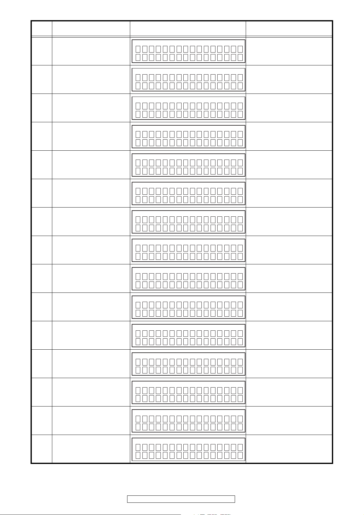
Error
code
5F
Details of Error code Display Coping strategies
Invalid data in firmware such as
Sub CPU, DSP, FPGA, and PLD
for rewriting sent from DM860
(invalid data received).
ub
S
pda t i ng fa i l 5F
U
***
mi n
Turn the power off then back on.
Updating starts automatically.
NACK received when “P” com-
60
mand sent to Sub CPU, DSP,
FPGA, PLD etc.
NACK received when “I” command
61
sent to Sub CPU, DSP, FPGA,
PLD etc.
Failure to acquire serial flash data
80
and before deleting serial flash.
Failure to delete data before rewrit-
81
ing serial flash.
Failure to receive firmware for
82
serial flash rewriting sent by
DM860 (when timed out).
Failure to receive firmware for
83
serial flash rewriting sent by
DM860 (when an error).
Failure to receive firmware for
84
serial flash rewriting sent by
DM860 (when a Check Sum error).
ub
S
pda t i ng fa i l 60
U
ub
S
pda t eCheckNG 61
U
UI Fl ash
G
pda t i ng fa i l 80
U
UI Fl ash
G
pda t i ng fa i l 81
U
UI Fl ash
G
pda t i ng fa i l 82
U
UI Fl ash
G
pda t i ng fa i l 83
U
UI Fl ash
G
pda t i ng fa i l 84
U
***
***
***
***
***
***
***
mi n
mi n
mi n
mi n
mi n
mi n
mi n
Turn the power off then back on.
Updating starts automatically.
Turn the power off then back on.
Updating starts automatically.
Turn the power off then back on.
Updating starts automatically.
Turn the power off then back on.
Updating starts automatically.
Turn the power off then back on.
Updating starts automatically.
Turn the power off then back on.
Updating starts automatically.
Turn the power off then back on.
Updating starts automatically.
Failure to receive firmware for
serial flash rewriting sent by
85
DM860 (when invalid data
received).
Failure to rewrite when writing data
86
in serial flash.
Failure to acquire (Application
A0
Mode) IP address before rewriting
DM860 (AutoIP).
Failure to acquire (Application
A1
Mode) IP address before rewriting
DM860 (when timed out).
Notification of invalid login via
DPMS access when rewriting
A2
DM860 related firmware (Application Mode).
Notification of line congestion via
DPMS access when rewriting
A3
DM860 related firmware (Application Mode).
Notification of connection failure
via DPMS access when rewriting
A4
DM860 related firmware (Application Mode).
UI Fl ash
G
pda t i ng fa i l 85
U
UI Fl ash
G
pda t i ng fa i l 86
U
ther IMG
E
onnec t i onFa i l A0
C
ther IMG
E
onnec t i onFa i l A1
C
ther IMG
E
og i n f a i l ed A2
L
ther IMG
E
erver is busyA3
S
ther IMG
E
onnec t i onFa i l A4
C
***
***
***
***
***
***
***
mi n
mi n
mi n
mi n
mi n
mi n
mi n
Turn the power off then back on.
Updating starts automatically.
Turn the power off then back on.
Updating starts automatically.
Check the network connection.
Carry out the update in an environment
that has little network load.
Check the network connection.
Carry out the update in an environment
that has little network load.
Check the network connection.
Carry out the update in an environment
that has little network load.
Check the network connection.
Carry out the update in an environment
that has little network load.
Check the network connection.
Carry out the update in an environment
that has little network load.
23
AVR-4310CI/AVR-4310/AVC-4310
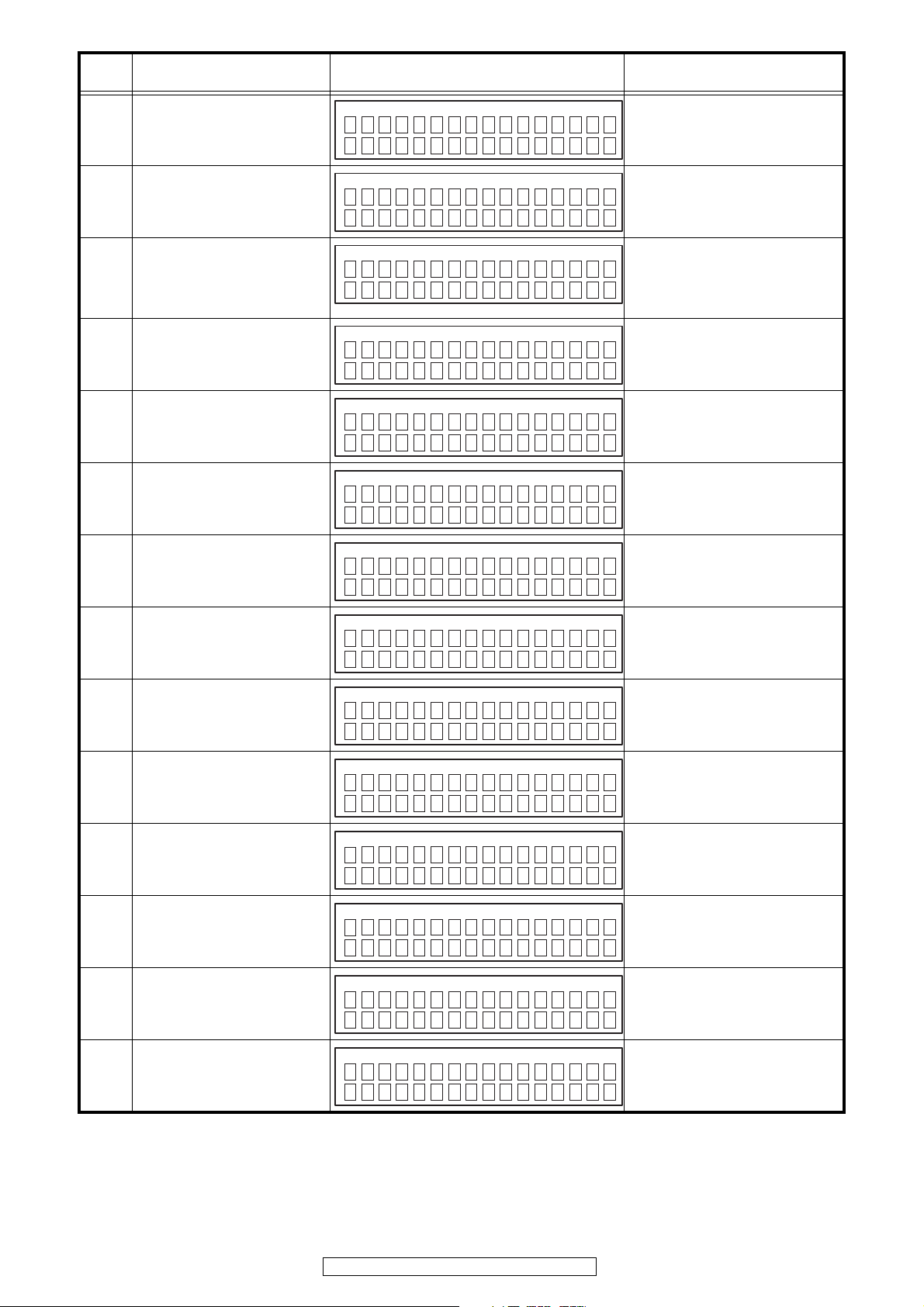
Error
code
A5
A6
A7
Details of Error code Display Coping strategies
Connection through DPMS access
timed out when rewriting DM860
related firmware (Application
Mode).
Firmware data error message
received after DPMS login when
rewriting DM860 related firmware
(Application Mode).
When rewriting DM860 related
firmware (Application Mode),
request was made for firmware
data after DPMS login but it timed
out.
ther IMG
E
onnec t i onFa i l A5
C
ther IMG
E
pda t i ng fa i l A6
U
ther IMG
E
pda t i ng fa i l A7
U
***
***
***
mi n
mi n
mi n
Check the network connection.
Carry out the update in an environment
that has little network load.
Turn the power off then back on.
Updating starts automatically.
Carry out the update in an environment
that has little network load.
Turn the power off then back on.
Updating starts automatically.
Carry out the update in an environment
that has little network load.
Failure to acquire (Boot Loader
A8
Mode) IP address before rewriting
DM860 (AutoIP).
Failure to acquire (Boot Loader
A9
Mode) IP address before rewriting
DM860 (when timed out).
Notification of invalid login via
DPMS access when rewriting
AA
DM860 related firmware (Boot
Loader Mode).
Notification of line congestion via
DPMS access when rewriting
AB
DM860 related firmware (Boot
Loader Mode).
Notification of connection failure
via DPMS access when rewriting
AC
DM860 related firmware (Boot
Loader Mode).
Connection through DPMS access
timed out when rewriting DM860
AD
related firmware (Boot Loader
Mode).
Firmware download error message
received (when download fails)
AE
when rewriting DM860 related firmware (Boot Loader Mode).
Firmware download error message
received (line congestion) when
AF
rewriting DM860 related firmware
(Boot Loader Mode).
Firmware download error message
received (connection failure) when
B0
rewriting DM860 related firmware
(Boot Loader Mode).
When rewriting DM860 related
firmware (Boot Loader Mode),
B1
request was made for firmware
download but it timed out .
Error message received when
B2
rewriting DM860 related firmware.
ther IMG
E
onnec t i onFa i l A8
C
ther IMG
E
onnec t i onFa i l A9
C
ther IMG
E
og i n f a i l ed AA
L
ther IMG
E
erver is busyAB
S
ther IMG
E
onnec t i onFa i l AC
C
ther IMG
E
onnec t i onFa i l AD
C
ther IMG
E
own l o ad f a i l AE
D
ther IMG
E
erver is busyAF
S
ther IMG
E
onnec t i onFa i lB0
C
ther IMG
E
own l o ad f a i l B1
D
ther IMG
E
pda t i ng fa i l B2
U
***
***
***
***
***
***
***
***
***
***
***
mi n
mi n
mi n
mi n
mi n
mi n
mi n
mi n
mi n
mi n
mi n
Check the network connection.
Carry out the update in an environment
that has little network load.
Check the network connection.
Carry out the update in an environment
that has little network load.
Check the network connection.
Carry out the update in an environment
that has little network load.
Check the network connection.
Carry out the update in an environment
that has little network load.
Check the network connection.
Carry out the update in an environment
that has little network load.
Check the network connection.
Carry out the update in an environment
that has little network load.
Turn the power off then back on.
Updating starts automatically.
Carry out the update in an environment
that has little network load.
Turn the power off then back on.
Updating starts automatically.
Carry out the update in an environment
that has little network load.
Turn the power off then back on.
Updating starts automatically.
Carry out the update in an environment
that has little network load.
Turn the power off then back on.
Updating starts automatically.
Carry out the update in an environment
that has little network load.
Turn the power off then back on.
Updating starts automatically.
Carry out the update in an environment
that has little network load.
24
AVR-4310CI/AVR-4310/AVC-4310
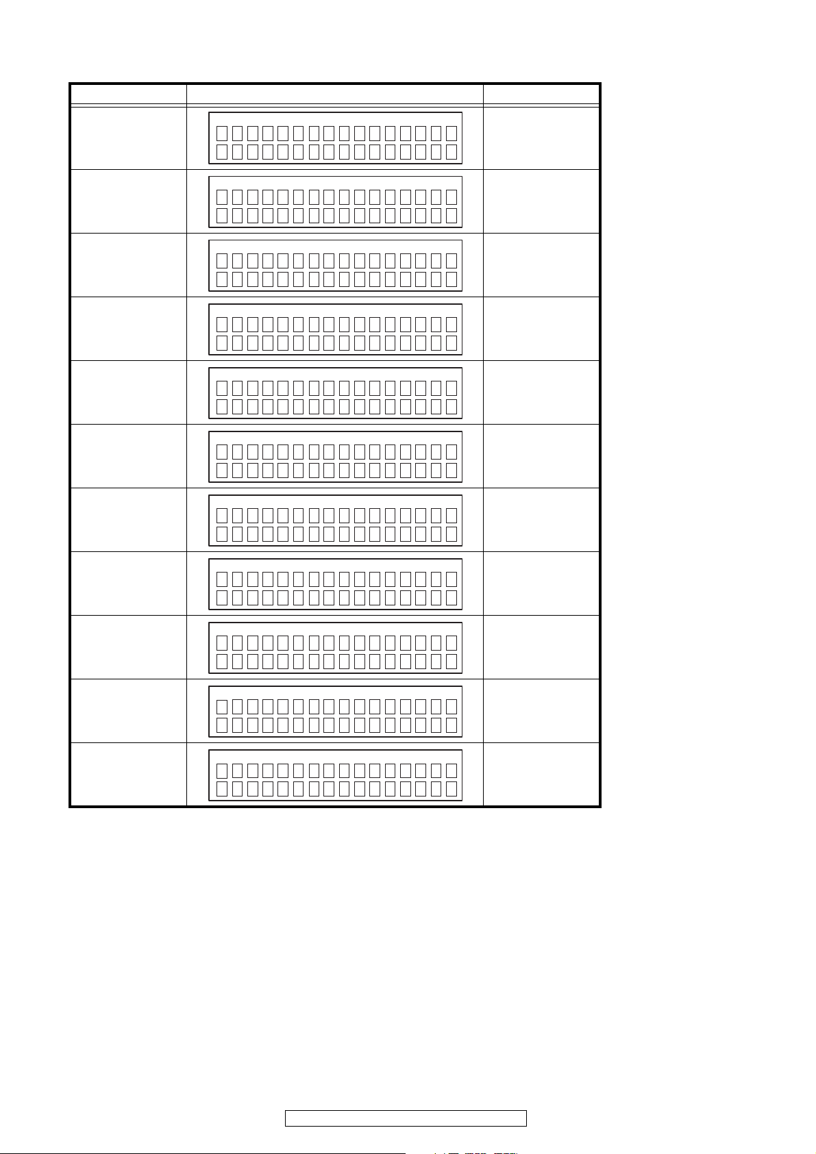
Device display when firmware updated
Target of devide when firmware updated.
Target of device Display Error cpde
Main
Main ROM
Sub
Audio PLD
Gui Config
Video PLD
DSP1
ain F i r m
M
pda t i ng
U
ain R O M
M
pda t i ng
U
ub
S
pda t i ng
U
PLD
A
pda t i ng
U
UI Conf
G
pda t i ng
U
PLD
V
pda t i ng
U
SP1
D
pda t i ng
U
***
***
***
***
***
***
***
mi n
mi n
mi n
mi n
mi n
mi n
mi n
30 〜 35
80 〜 86
50 〜 61
50 〜 61
50 〜 61
50 〜 61
50 〜 61
DSP2
Serial Flash
DM860 Boot Loader
DM860 Image
SP2
D
pda t i ng
U
UI Fl ash
G
pda t i ng
U
ther SBL
E
pda t i ng
U
ther IMG
E
pda t i ng
U
***
***
***
***
mi n
mi n
mi n
mi n
50 〜 61
80 〜 86
A0 〜 B2
A0 〜 B2
25
AVR-4310CI/AVR-4310/AVC-4310

ADJUSTMENT
Audio Section
Idling Current (8U-110049, 8U-110050-3)
Required measurement equipment: DC Voltmeter
Preparation
(1) Avoid direct blow from an air conditioner or an electric fan, and adjust the unit at normal room temperature 15°C ~ 30°C
(59°F ~ 86°F).
(2) Presetting
POWER (Power source switch) OFF
SPEAKER (Speaker terminal) No load
(Do not connect speaker, dummy resistor, etc.)
Adjustment
(1) Remove top cover and set VR101, VR201, VR301, VR401, VR501, VR601, VR701, on 8U-110049 (POWER AMP Unit)
at fully counterclockwise ( ).
(2) Connect DC Voltmeter to test points(8U-110050-3).
• FRONT-Lch: CX660 ③ ④ pin
• FRONT-Rch: CX660 ⑤ ⑥ pin
• CENTER ch: CX660 ① ② pin
• SURROUND-Lch: CX680 ⑤ ⑥ pin
• SURROUND-Rch: CX680 ⑦ ⑧ pin
• SURROUND BACK-Lch: CX680 ① ② pin
• SURROUND BACK-Rch: CX680 ③ ④ pin)
(3) Connect power cord to AC Line, and turn power switch "ON".
(4) Presetting.
MASTER VOLUME : "---" counterclockwise ( min.)
MODE : 7CH STEREO
FUNCTION : CD
(5) Allow 2 minutes, and turn VR101 clockwise ( ) to adjust the TEST POINT voltage to 6.5 mV ± 0.5 mV DC.
(6) After 10 minutes from preset, turn VR101 to set the voltage to 12 mV ± 0.5 mV DC.
(7) Adjust the Variable Resistors of other channels in the same way.
(8) After 5 minutes from (6), turn VR101 to set the voltage to 12 mV ± 0.5 mV DC.
(9) Adjust the Variable Resistors of other channels in the same way.
26
AVR-4310CI/AVR-4310/AVC-4310
DC Voltmeter
SBL ch
CX680
SBR ch
SR ch
SL ch
CX660
C ch
FR ch
FL ch
8U-310030 DIGITAL Unit
8U-110048-4 POWER SUPPLY Unit
VR501
VR701
VR601 VR101
VR301
VR401 VR201
Audio Section
Adjustment volume is set for 8U-110049-1 〜 7. The test point is at 8U-110050-3.
Insert an adjustment driver / connection terminal from an adjustment aperture of 8U-110048-4(POWER SUPPLY Unit)P.W.B..
27
AVR-4310CI/AVR-4310/AVC-4310
SURROUND MODES AND PARAMETERS
AAA
(NOTE1) S (Cinema) AA
Cinema EQ. Mode Room Size Effect Level
Back
Surround
1
z
AFDM
3
z
LFE
2
z
DRC
1
z
D. COMP
Signals and adjustability in the different modes
L/R
Front Height
L/R
Front Wide
z
Subwoofer
Back L/R
Surround
Channel output Parameter (default values are shown in parentheses)
L/R
Surround
vpage 74, 76).
vpage 73).
vpage 73).
vpage 76).
4 AAS(OFF) S (Auto) S (0 dB) AAAAAA
Center
SA A AD
L/R
Front
Surround Mode
PURE DIRECT, DIRECT (2ch)
SAAAAA AAAAAAAA A A
SDDDD A A A AS(0 dB) ASAAAA
SDDDD A A A AS(0 dB) S (ON) SAAAA
DSD DIRECT
DSD MULTI DIRECT
MULTI CH DIRECT
SA A AD A AS(OFF) S (Auto) S (0 dB) AAAAAA
STEREO
SDDDD D DS(OFF) S (Auto) S (0 dB) ASS(OFF) AAS(ON, 10)
SDDDDAAAAAAAAA A A
SDDDDD(NOTE4) D (NOTE4) AAS(0 dB) S (ON) SS(OFF) AAA
WIDE SCREEN
EXT. IN
DOLBY PRO LOGIC gz SDDAD A DS(OFF) S (Auto) S (0 dB) AAAS(Height) AA
MULTI CH IN
SDDDDD(NOTE4) D (NOTE4) S (OFF) S (Auto) AASS
DOLBY PRO LOGIC gx SDDDD A AS(OFF) S (Auto) AASS(NOTE1) S (Cinema) AA
DOLBY PRO LOGIC g SDDADD(NOTE4) D (NOTE4) S (OFF) S (Auto) AASS(NOTE2) S (Cinema) AA
DTS NEO:6
AVR-4310CI/AVR-4310/AVC-4310
SDDDDD(NOTE4) D (NOTE3) S (OFF) AS(0 dB) S (ON) SS(OFF) AAA
SDDDDD(NOTE4) D (NOTE3) S (OFF) AS(0 dB) S (ON) SS(OFF) AAA
SDDDDD(NOTE4) D (NOTE3) S (OFF) AS(0 dB) S (ON) SS(OFF) AAA
SDDDDD(NOTE4) D (NOTE3) S (OFF) AS(0 dB) S (ON) SS(OFF)
SDDDDD(NOTE4) D (NOTE4) AAAASAAAA
SDDDDD(NOTE4) D (NOTE3) S (OFF) AS(0 dB) S (ON) SS(OFF) AAA
SDDDDD(NOTE4) D (NOTE3) S (OFF) AS(0 dB) S (ON) SS(OFF) AAA
SDDDDD(NOTE4) D (NOTE3) AS(Auto) S (0 dB) S (ON) SS(OFF) AAA
DTS SURROUND
DTS 96/24
DOLBY DIGITAL
DOLBY DIGITAL Plus
DOLBY TrueHD
DTS-HD
SDDDD D DS(OFF) S (Auto) S (0 dB) ASAAAA
SDDDD D DS(OFF) S (Auto) S (0 dB) AS A AS(Medium) S (10)
SDDDD D DS(OFF) S (Auto) S (0 dB) AS A AS(Medium) S (10)
SDDDD D DS(OFF) S (Auto) S (0 dB) AS A AS(Medium) S (10)
DTS EXPRESS
neural
7CH STEREO
SUPER STADIUM
ROCK ARENA
JAZZ CLUB
28
SDDDD D DS(OFF) S (Auto) S (0 dB) AS A AS(Medium) S (10)
SDDDD D DS(OFF) S (Auto) S (0 dB) AS A AS(Medium) S (10)
SDDDD D DS(OFF) S (Auto) S (0 dB) AS A AS(Medium) S (10)
SDDDD D DS(OFF) S (Auto) S (0 dB) ASAAAA
SA A AD A AS(OFF) S (Auto) S (0 dB) AAAAAA
NOTE2 : This parameter is availabe when the “Mode” is set to “Cinema” or “ProLogic” (
D : Turned on or off by speaker configuration setting
NOTE1 : This parameter is availabe when the “Mode” is set to “Cinema” (
S : Signal / Adjustable
A : No signal / Not adjustable
CLASSIC CONCERT
MONO MOVIE
VIDEO GAME
MATRIX
VIRTUAL
1 : When playing Dolby Digital and DTS signals.
2 : When playing Dolby TrueHD signal.
NOTE:
3 : When playing Dolby Digital, DTS, DVD-Audio and Super Audio CD.z4 : When the “Subwoofer Mode” is set to “LFE+Main” (vpage 35) only.
z
z
z
NOTE3 : This parameter is availabe when the “Front Height” is set to “ON” or “DSX” is set to “ON” (
NOTE4 : This parameter is availabe when the “DSX” is set to “ON” (
RESTORER DSX
Volume
Dynamic
Tone Control MultEQ XT Dynamic EQ
Att.
Subwoofer
EXT. IN only
mode only
NEO:6 MUSIC
Signals and adjustability in the different modes
Parameter (default values are shown in parentheses)
PRO LOGIC g/gx MUSIC mode only
Delay Time Subwoofer Front Height
Panorama Dimension Center Width Center Image
ASAAAAAAAAAAAA
AAAAAAAAAAAAAA
AAAAAAAAAAAAAA
AAAAAAAAAAAAAA
AAAAAAAAS(OFF) S (OFF) SSSA
AASAAAAAS(OFF) S (OFF) SSAS
AASAAAAAS(OFF) S (OFF) SSAS
AAAAAAAAS(OFF) S (OFF) SSSA
AAAAAAASAAAAAA
AASAAAAAS(OFF) S (OFF) SSAS
AAAAAAS(0.3) AS(OFF) S (OFF) SSSS
AASAAAAAS(OFF) S (OFF) SSAS
AASAAAAAS(OFF) S (OFF) SSAS
AASAAAAAS(OFF) S (OFF) SSAS
AAAAAAAAS(NOTE5) S (OFF) SSS A
AAAAAAAAS(OFF) S (OFF) SSSA
AAAAAAAAS(OFF) S (OFF) SSSS
AASAAAAAS(OFF) S (OFF) SSAS
AASAAAAAS(OFF) S (OFF) SSAS
AAAAAAAAS(OFF) S (OFF) SSSA
AAAAAAAAS(NOTE6) S (OFF) SSS A
AAAAAAAAS(OFF) S (OFF) SSSA
S (30 ms) AAAAAAAS(OFF) S (OFF) SSS A
S : Signal / Adjustable
A : No signal / Not adjustable
NOTE5 : BASS +6 dB, TREBLE 0 dB
AAAAAAAAS(OFF) S (OFF) SSSA
AAAAAAAAS(OFF) S (OFF) SSSA
AAAAAAAAS(OFF) S (OFF) SSSA
NOTE6 : BASS +6 dB, TREBLE +4 dB
Surround Mode
PURE DIRECT, DIRECT (2ch)
DSD DIRECT
DSD MULTI DIRECT
MULTI CH DIRECT
STEREO
EXT. IN
MULTI CH IN
DOLBY PRO LOGIC gx AASS(OFF) S (3) S (3) AAS(OFF) S (OFF) SSS A
DOLBY PRO LOGIC gAASS(OFF) S (3) S (3) AAS(OFF) S (OFF) SSSS
DOLBY PRO LOGIC gz AASAAAAAS(OFF) S (OFF) SSS A
WIDE SCREEN
DOLBY DIGITAL Plus
DOLBY DIGITAL
DTS NEO:6
DOLBY TrueHD
DTS 96/24
DTS SURROUND
DTS-HD
7CH STEREO
neural
DTS EXPRESS
29
AVR-4310CI/AVR-4310/AVC-4310
SUPER STADIUM
ROCK ARENA
MONO MOVIE
CLASSIC CONCERT
JAZZ CLUB
VIDEO GAME
MATRIX
VIRTUAL
DOLBY
DOLBY
Input signals
DSD
DSD
PCM
PCM
DOLBY
DIGITAL
DOLBY
DIGITAL
DOLBY
DIGITAL
DIGITAL EX
DIGITAL
DOLBY
DIGITAL
DOLBY
DTS
(2ch)
(multi ch)
(2ch)
(multi ch)
(2ch)
(4/3ch)
(5.1/5/4ch)
Flag)
(With no
Flag)
EX (With
Plus
TrueHD
96/24
F : Mode selectable in initial status
D : Mode fixed when “AFDM” is “ON”
S : Selectable mode
A : Non-selectable mode
DTS
(5.1ch)
MTRX
DTS ES
DSCRT
DTS ES
DTS
EXPRESS
High
DTS-HD
Resolution
DTS-HD DTS DOLBY DOLBY DIGITAL MULTI CH PCM Super Audio CD
Master
DTS-HD
/
(Windows
Media Audio)
MP3 / MPEG-4
WMA
WAV
PCM /
LINEAR
ANALOG
Note
(With Flag)
(With Flag)
Audio
Audio
AAC / FLAC
AA A F A A A A AAAA A A A AA A A A A
AA A A F A A A AAAA A A A AA A A A A
AA A A A AF D A AAAA A A A AA A A A A
AA A A A A A F DAAAA A A A AA A A A A
AA A AA A S SFAAA A A AAAAAAA
AA A AA A A A AFAA A A AAAAAAA
AA A SS S S SSSAA A A AAAAAAA
AA A SS S S SSSAA A A AAAAAAA
AA A SS S S SSSAA A A AAAAAAA
AA A A A F A A AAAA A A A AA A A A A
AA A SS S A SSSAA A A AAAAAAA
SS S AA A A A AAAA A A A ASASAS
1
1
z
z
2
1
3
z
z
1
z
z
AA A AA A A A AAFAA A AAAAAAA
AA A A A A A A AAAF A A A AA A A A A
AA A AA A A A AAAAS S SSAAAAA
AA A AA A A A AASSA A AAAAAAA
AA A AA A A A AAAAS F FFAAAAA
AA A AA A A A AASSF DS SSAAAAA
AA A AA A A A AASSS S SSAAAAA
SS S AA A A A AAAA A A A ASASAS
1
1
z
2
z
z
AA A AA A A A AASSS S SSAAAAA
1
3
z
z
z
SS S AA A A A AAAA A A A ASASAS
SS S AA A A A AAAA A A A ASASAS
SS S AA A A A AAAA A A A ASASAS
SS S AA A A A AAAA A A A ASASAS
3
1
1
1
z
z
z
SS S AA A A A AAAA A A A ASASAS
SS S A A A A A AAAA A A A AA A S A A
1: This mode is not available when the surround back speaker setup is set to “None”.z2: This mode is not available when the surround back speaker setup is set to “1spkr” or “None”.z3: This mode is not available when the front height speaker setup is set to “None”.
z
NOTE:
Button
Surround Mode
STANDARD
DTS-HD MSTR
DTS SURROUND
DTS ES MTRX6.1
DTS ES DSCRT6.1
DTS SURROUND
DTS-HD HI RES
DTS 96/24
DTS (–HD) + PLgx CINEMA
DTS (–HD) + PLgx MUSIC
DTS (–HD) + PLgz HEIGHT
DTS EXPRESS
DTS (–HD) + NEO:6
DTS NEO:6 CINEMA
DTS NEO:6 MUSIC
DOLBY TrueHD
DOLBY DIGITAL+
DOLBY DIGITAL EX
DOLBY (D+) (HD) +EX
DOLBY DIGITAL
DOLBY SURROUND
30
AVR-4310CI/AVR-4310/AVC-4310
DOLBY (D) (D+) (HD) +PLgx
CINEMA
DOLBY (D) (D+) (HD) +PLgx
MUSIC
DOLBY (D) (D+) (HD) +PLgz
HEIGHT
DOLBY PRO LOGIC gx CINEMA
DOLBY PRO LOGIC gz HEIGHT
DOLBY PRO LOGIC gx MUSIC
DOLBY PRO LOGIC gx GAME
DOLBY PRO LOGIC g CINEMA SS S AA A A A AAAA A A A ASASAS
DOLBY PRO LOGIC g MUSIC SS S A A A A A AAAA A A A ASASAS
DOLBY PRO LOGIC g GAME SS S AA A A A AAAA A A AASASAS
DOLBY PRO LOGIC
neural

DSD
DSD
(2ch)
(multi ch)
DOLBY
DOLBY
Input signals
PCM
PCM
DOLBY
DIGITAL
DOLBY
DIGITAL
DOLBY
DIGITAL
DIGITAL EX
DIGITAL
DOLBY
DIGITAL
DOLBY
DTS
DTS
(2ch)
(multi ch)
(2ch)
(4/3ch)
(5.1/5/4ch)
Flag)
(With no
Flag)
EX (With
Plus
TrueHD
96/24
(5.1ch)
AAA
(7.1)
AAA
(7.1)
AAA
(7.1)
F : Mode selectable in initial status
S : Selectable mode
A : Non-selectable mode
MTRX
DTS ES
DSCRT
DTS ES
DTS
EXPRESS
High
DTS-HD
Resolution
DTS-HD DTS DOLBY DOLBY DIGITAL MULTI CH PCM Super Audio CD
Master
DTS-HD
/
(Windows
Media Audio)
MP3 / MPEG-4
WMA
WAV
PCM /
LINEAR
ANALOG
Note
(With Flag)
(With Flag)
Audio
Audio
AAC / FLAC
AA A A A A A A AAAA A A A AA S A S A
AA A A A A A A AAAA A A A AA F A F A
2
z
AA A A A A A A AAAA A A A AA S A S A
AA A A A A A A AAAA A A A AA S A S A
1
3
z
z
AA A A A A A A AAAA A A A AA S A S A
AA A A A A A A AAAA A A A AAFD
1
1
z
z
AA A A A A A A AAAA A A A AA A A A S
SS S S S S S S SSSS S S S SS A S A S
AA A A A A A A AAAA A A A AA A A S A
AA A A A A A A AAAA A A A AA S A S A
AA A A A A A A AAAA A A A AA S A S A
AA A A A A A A AAAA A A A AA S A S A
1
2
z
z
AA A A A A A A AAAA A A A AA S A S A
AA A A A A A A AAAA A A A AA S A S A
3
1
z
z
AA A A A A A A AAAA A A A AAS
1
z
NOTE :
1: This mode is not available when the surround back speaker setup is set to “None”.z2: This mode is not available when the surround back speaker setup is set to “1spkr” or “None”.z3: This mode is not available when the front height speaker setup is set to “None”.
z
Button
Surround Mode
STANDARD
MULTI CH IN
MULTI CH IN
MULTI IN + PLgx MUSIC
MULTI IN + PLgx CINEMA
MULTI IN + PLgz HEIGHT
MULTI IN + DOLBY EX
MULTI CH IN 7.1
M DIRECT + PLgz HEIGHT
M DIRECT + DOLBY EX
DIRECT
DIRECT
DSD DIRECT
DSD MULTI DIRECT
MULTI CH DIRECT
M DIRECT + PLgx MUSIC
M DIRECT + PLgx CINEMA
M DIRECT 7.1
PURE DIRECT
PURE DIRECT
DSD PURE DIRECT
31
AVR-4310CI/AVR-4310/AVC-4310
M PURE D + PLgz HEIGHT
DSD MULTI PURE DIRECT
M PURE D + PLgx MUSIC
MULTI CH PURE DIRECT
M PURE D + PLgx CINEMA
M PURE D + DOLBY EX
M CH PURE DIRECT 7.1

DOLBY
DOLBY
Input signals
DSD
DSD
PCM
PCM
DOLBY
DIGITAL
DOLBY
DIGITAL
DOLBY
DIGITAL
DIGITAL EX
DIGITAL
DOLBY
DIGITAL
DOLBY
DTS
(2ch)
(multi ch)
(2ch)
(multi ch)
(2ch)
(4/3ch)
(5.1/5/4ch)
Flag)
(With no
Flag)
EX (With
Plus
TrueHD
96/24
DTS
(5.1ch)
MTRX
DTS ES
DSCRT
DTS ES
DTS
EXPRESS
High
DTS-HD
Resolution
DTS-HD DTS DOLBY DOLBY DIGITAL MULTI CH PCM Super Audio CD
Master
DTS-HD
/
(Windows
Media Audio)
MP3 / MPEG-4
WMA
WAV
PCM /
LINEAR
ANALOG
Note
(With Flag)
(With Flag)
Audio
Audio
AAC / FLAC
SS S S S S S S SSSS S S S SS S S S S
SS S S S S S S SSSS S S S SS S S S S
4
z
SS S S S S S S SSSS S S S SS S S S S
SS S S S S S S SSSS S S S SS S S S S
SS S S S S S S SSSS S S S SS S S S S
SS S S S S S S SSSS S S S SS S S S S
SS S S S S S S SSSS S S S SS S S S S
SS S S S S S S SSSS S S S SS S S S S
SS S S S S S S SSSS S S S SS S S S S
SS S S S S S S SSSS S S S SS S S S S
FF F S S S S S SSSS S S S SF S F S F
NOTE :
4 : If the surround back, front wide and front height speaker setup is set to “None”, then “5CH STEREO” is displayed.
z
Button
Surround Mode
DSP SIMULATION
WIDE SCREEN
SUPER STADIUM
7CH STEREO
CLASSIC CONCERT
ROCK ARENA
JAZZ CLUB
MONO MOVIE
VIDEO GAME
MATRIX
VIRTUAL
STEREO
STEREO
32
AVR-4310CI/AVR-4310/AVC-4310
TROUBLE SHOOTING
1. POWER
1.1. Power not turn on
Power not turn on
YES
Is the ON/STANDBY indicator on the front panel flashing
red?
YES
Is the fuse blown?
YES
Does the power turn on when
the POWER switch is turned
off then back on?
YES YES YES
Check the primary circuitry
parts including the POWER
switch (for poor contacts,
etc.), and replace any defective parts.
Are there any incomplete
connections in the connec-
NO
tors connecting between the
various circuit boards?
YES YES
Connect the connectors
properly.
NO
NO
Refer to Fuse is blown
Is a DC 5V voltage being
supplied from the 8U-110048
board (CW068 pin 1) to the
microprocessor?
Check the 8U-210064
board's microprocessor
periphery circuitry and
replace any defective parts.
Is there a short circuit
NO
between the speaker terminals and the ground?
Check for damage in the
power amplifier circuitry parts
and replace any defective
parts.
Is a DC 5V voltage output
when the cord supplying the
NO
power from the 8U-110048
board to the microprocessor
(CX068) is unplugged?
Check the circuitry and parts
from CW068 on the 8U110048 board to the microprocessor for damage and
short-circuits, and replace
any defective parts.
Correct the short circuit
NO
between the speaker and
the ground.
Check the parts from IC901
NO
to the primary circuitry and
replace any defective parts.
1.2. Fuse is blown
YES YES YES
Check for leaks or short circuits in the primary side
parts, and replace any defective parts.
YES YES YES
Fuse is blown
Check for short circuits in the
rectifier diodes and circuitry
of the secondary side rectifying circuits, and replace any
defective parts.
After repairing, also replace the fuse.
Check for short circuits in the
power stabilizer unit's regulator output terminal and the
ground, and replace any
defective parts.
33
AVR-4310CI/AVR-4310/AVC-4310

2. Analog video
2.1. MONITOR OUT (CVBS) output NG
Checking the video convert ON/OFF settings
Video convert ON Video convert OFF
Input
CVBS
Input
S
AB
Interlace
C
MONITOR OUT (CVBS) output NG
Input
COMPONENT
Interlace
o r
Progressive
Progressive
no output
※ When checking operation,
select DVD for the function.
(COMPONENT1 input)
Input
CVBS
Input
S
Input
COMPONENT
D No output No output
34
AVR-4310CI/AVR-4310/AVC-4310

A
Input
CVBS
YES
Check ± 5VA and +5VD.
+5VA : CY152-13,14pin
-5VA : CY152-12pin
+5VD : CX141-1pin
OK
Check input/output of analog SW.
Input : IC109-13pin
Output : IC109-3pin
OK
To troubleshooting 1.1 Power not
NG
turn on.
NG
Check analog SW settings.
IC109-9,10,11pin : L(0V)
IC109-6pin : L(0V)
OK
Check soldering of IC109.
Check IC301, IC303 and CX141
NG
soldering, or DIGITAL UNIT flaw.
Check input/output of AMP.
Input : IC115-5pin
Output : IC115-7pin
OK
Check output to 8U-310030 DIGITAL
UNIT.
Output V : CX111-1pin
OK
Check input of video driver.
Input Y : IC305-2pin
Input C : IC305-4pin
OK
Check output of video driver.
Output V : IC305-36pin
OK
Check input/output of analog SW.
Input : IC108-14pin
Output : IC108-13pin
OK
Check soldering of IC115 and
NG
surrounding parts.
NG
NG
NG
NG
Check soldering of CX111.
Check CX151 soldering, or digital
unit flaw.
Check soldering of IC305.
Check analog SW settings.
IC108-10pin : H(+5V)
IC108-9pin : L(0V)
OK
Check soldering of IC108.
Check IC301 and CX141 solder-
NG
ing, or DIGITAL UNIT flaw.
Check input/output of AMP.
Input : IC112-5pin
Output : IC112-7pin
OK
Check cable between main unit and monitor or Check monitor.
NG
※ Unless specified, 8U-210063-1 A.VIDEO UNIT part.
AVR-4310CI/AVR-4310/AVC-4310
Check soldering of IC112.
35

B
Input
S
YES
Check ± 5VA and +5VD.
+5VA : CY152-13,14pin
-5VA : CY152-12pin
+5VD : CX141-1pin
OK
Check input/output of analog SW.
Input Y : IC102-13pin
Input C : IC106-13pin
Output Y : IC102-3pin
Output C : IC106-3pin
OK
Check input/output of AMP.
Input Y : IC113-5pin
Input C : IC114-5pin
Output Y : IC113-7pin
Output C : IC114-7pin
OK
Check output to 8U-310030 DIGITAL
UNIT.
Output Y : CX111-9pin
Output C : CX111-11pin
To troubleshooting 1.1 Power not
NG
turn on.
Check analog SW settings.
NG
NG
NG
IC102-9,10,11pin : L(0V)
IC102-6pin : L(0V)
IC106-9,10,11pin : L(0V)
IC106-6pin : L(0V)
OK
Check soldering of IC102 and IC106.
Check soldering of IC113, IC114
and surrounding parts.
Check soldering of CX111.
Check IC301, IC303 and CX141
NG
soldering, or DIGITAL UNIT flaw.
OK
Check input of video driver
Input Y : IC305-2pin
Input C : IC305-4pin
OK
Check output of video driver.
Output V : IC305-36pin
OK
Check input/output of analog SW.
Input : IC108-14pin
Output : IC108-13pin
OK
Check input/output of AMP.
Input : IC112-5pin
Output : IC112-7pin
OK
Check cable between main unit and monitor or Check monitor.
Check CX151 soldering, or
NG
DIGITAL UNIT flaw.
NG
NG
NG
Check soldering of IC305.
Check analog SW settings.
IC108-10pin : H(+5V)
IC108-9pin : L(0V)
Check soldering of IC108.
Check soldering of IC112.
OK
Check IC301 and CX141 solder-
NG
ing, or DIGITAL UNIT flaw.
※ Unless specified, 8U-210063-1 A.VIDEO UNIT part.
36
AVR-4310CI/AVR-4310/AVC-4310

C
Input
COMPONENT
YES
Check ± 5VA, +5VD and +9VA.
+5VA : CY152-13,14pin
-5VA : CY152-12pin
+5VD : CX141-1pin
+9VA : CY152-15pin
OK
Check input/output of COMPONENT
selector.
Input Y : IC501-48pin
Input Cb : IC501-2pin
Input Cr : IC501-4pin
Output Y : IC501-27pin
Output Cb : IC501-24pin
Output Cr : IC501-21pin
OK
Check input/output of AMP.
Input Y : IC503-1pin
Input Cb : IC503-3pin
Input Cr : IC503-5pin
Output Y : IC503-13pin
Output Cb : IC503-11pin
Output Cr : IC503-9pin
To troubleshooting 1.1 Power not
NG
turn on.
Check IC501 and CX141
NG
soldering, or DIGITAL UNIT flaw.
Check IC503 soldering, or AMP
NG
settings.
IC503-7pin : H(5V)
OK
Check output to 8U-310030 DIGITAL
UNIT.
Output Y : CX111-7pin
Output Cb : CX111-5pin
Output Cr : CX111-3pin
Check input of video driver
Input Y : IC305-2pin
Input C : IC305-4pin
OK
Check output of video driver.
Output V : IC305-36pin
OK
Check input/output of analog SW.
Input : IC108-14pin
Output : IC108-13pin
OK
Check soldering of IC503 and
surrounding parts.
NG
NG
NG
NG
Check soldering of CX111.
Check CX151 soldering,
or DIGITAL UNIT flaw.
Check soldering of IC305.
Check analog SW settings.
IC108-10pin : H(+5V)
IC108-9pin : L(0V)
Check soldering of IC108.
OK
OK
Check IC301 and CX141 solder-
NG
ing, or DIGITAL UNIT flaw.
Check input/output of AMP.
Input : IC112-5pin
Output : IC112-7pin
OK
Check cable between main unit and monitor or Check monitor.
NG
※ Unless specified, 8U-210063-1 A.VIDEO UNIT part.
AVR-4310CI/AVR-4310/AVC-4310
Check soldering of IC112.
37

D
Input
CVBS
YES
Check ± 5VA and +5VD.
+5VA : CY152-13,14pin
-5VA : CY152-12pin
+5VD : CX141-1pin
OK
Check input/output of analog SW.
Input : IC109-13pin
Output : IC109-3pin
OK
To troubleshooting 1.1 Power not
NG
turn on.
NG
Check analog SW settings.
IC109-9,10,11pin : L(0V)
IC109-6pin : L(0V)
OK
Check soldering of IC109.
Check IC301, IC303 and CX141
NG
soldering, or DIGITAL UNIT flaw.
Check input/output of AMP.
Input : IC115-5pin
Output : IC115-7pin
OK
Check input/output of analog SW.
Input : IC108-15pin
Output : IC108-13pin
OK
Check input/output of AMP.
Input : IC112-5pin
Output : IC112-7pin
OK
Check cable between main unit and monitor or Check monitor.
NG
NG
NG
※ Unless specified, 8U-210063-1 A.VIDEO UNIT part.
Check soldering of IC115.
Check analog SW settings.
IC108-10pin : L(0V)
IC108-9pin : H(+5V)
OK
Check soldering of IC108.
Check soldering of IC112.
Check soldering of IC301 and
NG
CX141.
38
AVR-4310CI/AVR-4310/AVC-4310

2.2. ZONE2 MONITOR OUT (CVBS) Output NG
ZONE2 MONITOR OUT (CVBS) Output NG.
Check ZONE2 is power on.
OK
I n p u t
CVBS
Input
S
I n p u t
COMPONENT
※ When checking operation,
select DVD for the function.
Turn on ZONE2 and check
NG
EFNo output
again.
39
AVR-4310CI/AVR-4310/AVC-4310

E
Input
CVBS
YES
Check ± 5VA and +5VD.
+5VA : CY152-13,14pin
-5VA : CY152-12pin
+5VD : CX141-1pin
OK
Check input/output of analog SW.
Input : IC110-13pin
Output : IC110-3pin
OK
To troubleshooting 1.1 Power not
NG
turn on.
NG
Check analog SW settings.
IC110-9,10,11pin : L(0V)
IC110-6pin : L(0V)
OK
Check soldering of IC110.
Check IC301, IC303 and CX141
NG
soldering, or DIGITAL UNIT flaw.
Check input/output of AMP.
Input : IC115-3pin
Output : IC115-1pin
OK
Check input/output to OSD driver input
signal selector.
Input : IC202-5pin
Output : IC202-4pin
OK
Check input/output of OSD driver.
Input : IC201-15pin
Output : IC201-13pin
OK
Check input/output of buffer AMP.
Input : IC203-3pin
Output : IC203-1pin
OK
Check input/output of analog SW.
Input : IC105-15pin
Output : IC105-3pin
NG
NG
NG
NG
NG
Check soldering of IC115.
Check analog SW settings.
IC202-9,10,11pin : L(0V)
Check soldering of IC202.
Check soldering of IC201 and
surrounding parts.
Check soldering of IC203.
Check analog SW settings.
IC105-11pin : L(0V)
IC105-10pin : H(+5V)
OK
Check IC303 and CX141 solder-
NG
ing, or DIGITAL UNIT flaw.
Check IC303 and CX141 solder-
NG
ing, or DIGITAL UNIT flaw.
OK
Check input/output of AMP.
Input : IC112-3pin
Output : IC112-1pin
OK
Check cable between main unit and monitor or Check monitor.
NG
※ Unless specified, 8U-210063-1 A.VIDEO UNIT part.
AVR-4310CI/AVR-4310/AVC-4310
OK
Check soldering of IC105.
Check soldering of IC112.
40

F
Input
S
YES
Check ± 5VA and +5VD.
+5VA : CY152-13,14pin
-5VA : CY152-12pin
+5VD : CX141-1pin
OK
Check input/output of analog SW.
Input Y : IC103-13pin
Input C : IC107-13pin
Output Y : IC103-3pin
Output C : IC107-3pin
OK
Check input/output of AMP.
Input Y : IC113-3pin
Input C : IC114-3pin
Output Y : IC113-1pin
Output C : IC114-1pin
OK
Check input/output of MIX AMP.
Input Y : IC116-3pin
Input C : IC116-1pin
To troubleshooting 1.1 Power not
NG
turn on.
NG
NG
NG
Check analog SW settings.
IC103-9,10,11pin : L(0V)
IC107-9,10,11pin : L(0V)
OK
Check soldering of IC103 and IC107.
Check soldering of IC113, IC114
and surrounding parts.
Check soldering of IC116.
Check IC301, IC303 and CX141
NG
soldering, or DIGITAL UNIT flaw.
OK
Check input/output to OSD driver input
signal selector.
Input : IC202-3pin
Output : IC202-4pin
OK
Check input/output of OSD driver.
Input : IC201-15pin
Output : IC201-13pin
OK
Check input/output of buffer AMP.
Input : IC203-3pin
Output : IC203-1pin
OK
Check input/output of analog SW.
Input : IC105-15pin
Output : IC105-3pin
OK
NG
NG
NG
NG
Check analog SW settings.
IC202-9,10,11pin : H(+5V)
Check soldering of IC202.
Check soldering of IC201 and
surrounding parts.
Check soldering of IC203.
Check analog SW settings.
IC105-11pin : L(0V)
IC105-10pin : H(+5V)
Check soldering of IC105.
OK
OK
Check IC303 and CX141 solder-
NG
ing, or DIGITAL UNIT flaw.
Check IC303 and CX141 solder-
NG
ing, or DIGITAL UNIT flaw.
Check input/output of AMP.
Input : IC112-3pin
Output : IC112-1pin
OK
Check cable between main unit and monitor or Check monitor.
NG
※ Unless specified, 8U-210063-1 A.VIDEO UNIT part.
AVR-4310CI/AVR-4310/AVC-4310
Check soldering of IC112.
41

2.3. VCR/DVR MONITOR OUT(CVBS) Output NG
VCR/DVR MONITOR OUT(CVBS) Output NG.
I n p u t
CVBS
VCR : G
Input
S
No output No output
DVR : H
※ When checking operation,
select DVD for the function.
I n p u t
COMPONENT
42
AVR-4310CI/AVR-4310/AVC-4310

G
Input
CVBS
YES
Check ± 5VA and +5VD.
+5VA : CY152-13,14pin
-5VA : CY152-12pin
+5VD : CX141-1pin
OK
Check input/output of analog SW.
Input : IC110-13pin
Output : IC110-3pin
OK
To troubleshooting 1.1 Power not
NG
turn on.
NG
Check analog SW settings.
IC110-9,10,11pin : L(0V)
IC110-6pin : L(0V)
OK
Check soldering of IC110.
Check IC301, IC303 and CX141
NG
soldering, or DIGITAL UNIT flaw.
Check input/output of AMP.
Input : IC115-3pin
Output : IC115-1pin
OK
Check input/output of video driver.
Input : IC101-12pin
Output : IC101-24pin
OK
Check cable between main unit and monitor or Check monitor.
NG
NG
※ Unless specified, 8U-210063-1 A.VIDEO UNIT part.
Check soldering of IC115.
Check video driver settings.
IC101-16pin : H(5V)
OK
Check soldering of IC101.
Check IC303 and CX141 solder-
NG
ing, or DIGITAL UNIT flaw.
43
AVR-4310CI/AVR-4310/AVC-4310

H
Input
CVBS
YES
Check ± 5VA +and 5VD.
+5VA : CY152-13,14pin
-5VA : CY152-12pin
+5VD : CX141-1pin
OK
Check input/output of analog SW.
Input : IC110-13pin
Output : IC110-3pin
OK
To troubleshooting 1.1 Power not
NG
turn on.
NG
Check analog SW settings.
IC110-9,10,11pin : L(0V)
IC110-6pin : L(0V)
OK
Check soldering of IC110.
Check IC301, IC303 and CX141
NG
soldering, or DIGITAL UNIT flaw.
Check input/output of AMP.
Input : IC115-3pin
Output : IC115-1pin
OK
Check input/output of video driver.
Input : IC101-3pin
Output :IC101-33pin
OK
Check cable between main unit and monitor or Check monitor.
NG
NG
※ Unless specified, 8U-210063-1 A.VIDEO UNIT part.
Check soldering of IC115.
Check video driver settings.
IC101-7pin : H(5V)
OK
Check soldering of IC101.
Check IC303 and CX141 solder-
NG
ing, or DIGITAL UNIT flaw.
44
AVR-4310CI/AVR-4310/AVC-4310

2.4. MONITOR OUT (S) Output NG
Video convert ON Video convert OFF
Input
CVBS
Input
S
IJ
Interlace
K
MONITOR OUT (S) Output NG
Checking the video convert ON/OFF settings
Input
COMPONENT
Interlace
o r
Progressive
Progressive
No output
Input
CVBS
No output L No output
※ When checking operation,
select DVD for the function.
(COMPONENT1 Input)
Input
S
Input
COMPONENT
45
AVR-4310CI/AVR-4310/AVC-4310

I
Input
CVBS
YES
Check ± 5VA and +5VD.
+5VA : CY152-13,14pin
-5VA : CY152-12pin
+5VD : CX141-1pin
OK
Check input/output of analog SW.
Input : IC109-13pin
Output : IC109-3pin
OK
To troubleshooting 1.1 Power not
NG
turn on.
NG
Check analog SW settings.
IC109-9,10,11pin : L(0V)
IC109-6pi : L(0V)
OK
Check soldering of IC109.
Check IC301, IC303 and CX141
NG
soldering, or DIGITAL UNIT flaw.
Check input/output of AMP.
Input : IC115-5pin
Output : IC115-7pin
OK
Check output to 8U-310030 DIGITAL
UNIT.
Output V : CX111-1pin
OK
Check input of video driver.
Input Y : IC305-2pin
Input C : IC305-4pin
OK
Check output of video driver.
Output Y : IC305-34pin
Output C : IC305-32pin
OK
Check input/output of analog SW.
Input Y : IC104-5pin
Input C : IC104-14pin
Output Y : IC104-3pin
Output C : IC104-13pin
Check soldering of IC115 and
NG
surrounding parts.
NG
NG
NG
NG
Check soldering of CX111.
Check CX151 soldering, or DIGITAL
UNIT flaw.
Check soldering of IC305.
Check analog SW settings.
IC104-10pin : H(+5V)
IC104-9pin : L(0V)
OK
Check IC301 and CX141 solder-
NG
ing, or DIGITAL UNIT flaw.
OK
Check input/output of AMP.
Input Y: IC111-3pin
Input C: IC111-5pin
Output Y : IC111-1pin
Output C : IC111-7pin
OK
Check cable between main unit and monitor or Check monitor.
NG
※ Unless specified, 8U-210063-1 A.VIDEO UNIT part.
AVR-4310CI/AVR-4310/AVC-4310
Check soldering of IC104.
Check soldering of IC111.
46

J
Input
S
YES
Check ±5VA and +5VD.
+5VA : CY152-13,14pin
-5VA : CY152-12pin
+5VD : CX141-1pin
OK
Check input/output of analog SW.
Input Y : IC102-13pin
Input C : IC106-13pin
Output Y : IC102-3pin
Output C : IC106-3pin
OK
Check input/output of AMP.
Input Y : IC113-5pin
Input C : IC114-5pin
Output Y : IC113-7pin
Output C : IC114-7pin
OK
Check output to 8U-310030 DIGITAL
UNIT.
Output Y : CX111-9pin
Output C : CX111-11pin
To troubleshooting 1.1 Power not
NG
turn on.
Check analog SW settings.
NG
NG
NG
IC102-9,10,11pin : L(0V)
IC102-6pin : L(0V)
IC106-9,10,11pin : L(0V)
IC106-6pin : L(0V)
OK
Check soldering of IC102 and IC106.
Check soldering of IC113, IC114
and surrounding parts.
Check soldering of CX111.
Check IC301, IC303 and CX141
NG
soldering, or DIGITAL UNIT flaw.
OK
Check input of video driver
Input Y : IC305-2pin
Input C : IC305-4pin
OK
Check output of video driver.
Output Y : IC305-34pin
Output C : IC305-32pin
OK
Check input/output of analog SW.
Input Y : IC104-5pin
Input C : IC104-14pin
Output Y : IC104-3pin
Output C : IC104-13pin
OK
Check input/output of AMP.
Input Y : IC111-3pin
Input C : IC111-5pin
Output Y : IC111-1pin
Output C : IC111-7pin
Check CX151 soldering, or DIGITAL
NG
UNIT flaw.
NG
NG
NG
Check soldering of IC305.
Check analog SW settings.
IC104-10pin : H(+5V)
IC104-9pin : L(0V)
OK
Check soldering of IC104.
Check soldering of IC111.
Check IC301 and CX141 solder-
NG
ing, or DIGITAL UNIT flaw.
OK
Check cable between main unit and monitor or Check monitor.
※ Unless specified, 8U-210063-1 A.VIDEO UNIT part.
AVR-4310CI/AVR-4310/AVC-4310
47

K
Input
COMPONENT
YES
Check ± 5VA, +5VD and +9VA.
+5VA : CY152-13,14pin
-5VA : CY152-12pin
+5VD : CX141-1pin
+9VA : CY152-15pin
OK
Check input/output of COMPONENT
selector.
Input Y : IC501-48pin
Input Cb : IC501-2pin
Input Cr : IC501-4pin
Output Y : IC501-27pin
Output Cb : IC501-24pin
Output Cr : IC501-21pin
OK
Check input/output of AMP.
Input Y : IC503-1pin
Input Cb : IC503-3pin
Input Cr : IC503-5pin
Output Y : IC503-13pin
Output Cb : IC503-11pin
Output Cr : IC503-9pin
OK
To troubleshooting 1.1 Power not
NG
turn on.
Check IC501 and CX141 soldering,
NG
or DIGITAL UNIT flaw.
Check IC503 soldering, or check
NG
AMP settings.
IC503-7pin : H(5V)
OK
Check soldering of IC503 and
surrounding parts.
Check output to 8U-310030 DIGITAL
UNIT.
Output Y : CX111-7pin
Output Cb : CX111-5pin
Output Cr : CX111-3pin
OK
Check input of video driver
Input Y : IC305-2pin
Input C : IC305-4pin
OK
Check output of video driver.
Output Y : IC305-34pin
Output C : IC305-32pin
OK
Check input/output of analog SW.
Input Y : IC104-5pin
Input C : IC104-14pin
Output Y : IC104-3pin
Output C : IC104-13pin
OK
Check input/output of AMP.
Input Y : IC111-3pin
Input C : IC111-5pin
Output Y : IC111-1pin
Output C : IC111-7pin
OK
Check cable between main unit and monitor or Check monitor .
NG
Check CX151 soldering, or DIGITAL
NG
UNIT flaw.
NG
NG
NG
※ Unless specified, 8U-210063-1 A.VIDEO UNIT part.
Check soldering of CX111.
Check soldering of IC305.
Check analog SW settings.
IC104-10pin : H(+5V)
IC104-9pin : L(0V)
OK
Check soldering of IC104.
Check soldering of IC111.
Check IC301 and CX141 soldering,
NG
or DIGITAL UNIT flaw.
48
AVR-4310CI/AVR-4310/AVC-4310

L
Input
S
YES
Check ± 5VA and +5VD.
+5VA : CY152-13,14pin
-5VA : CY152-12pin
+5VD : CX141-1pin
OK
Check input/output of analog SW.
Input Y : IC102-13pin
Input C : IC106-13pin
Output Y : IC102-3pin
Output C : IC106-3pin
OK
Check input/output of AMP.
Input Y : IC113-5pin
Input C : IC114-5pin
Output Y : IC113-7pin
Output C : IC114-7pin
OK
Check input/output of analog SW.
Input Y : IC104-2pin
Input C : IC104-15pin
Output Y : IC104-3pin
Output C : IC104-13pin
To troubleshooting 1.1 Power not
NG
turn on.
Check analog SW settings.
NG
NG
NG
IC102-9,10,11pin : L(0V)
IC102-6pin : L(0V)
IC106-9,10,11pin : L(0V)
IC106-6pin : L0V)
OK
Check soldering of IC102 and IC106.
Check soldering of IC113, IC114
and surrounding parts.
Check analog SW settings.
IC104-10pin : L(0V)
IC104-9pin : H(+5V)
Check IC301, IC303 and CX141
NG
soldering, or DIGITAL UNIT flaw.
Check IC301 and CX141 solder-
NG
ing, or DIGITAL UNIT flaw.
OK
Check input/output of AMP.
Input Y : IC111-3pin
Input C : IC111-5pin
Output Y : IC111-1pin
Output C : IC111-7pin
OK
Check cable between main unit and monitor or Check monitor .
NG
※ Unless specified, 8U-210063-1 A.VIDEO UNIT part.
OK
Check soldering of IC104.
Check soldering of IC111.
49
AVR-4310CI/AVR-4310/AVC-4310

2.5. VCR/DVR MONITOR OUT(S) Output NG
VCR/DVR MONITOR OUT(S) Output NG.
I n p u t
CVBS
No output
Input
S
VCR : M
DVR : N
※ When checking operation,
select DVD for the function.
I n p u t
COMPONENT
No output
50
AVR-4310CI/AVR-4310/AVC-4310

M
Input
S
YES
Check ± 5VA and +5VD.
+5VA : CY152-13,14pin
-5VA : CY152-12pin
+5VD : CX141-1pin
OK
Check input/output of analog SW.
Input Y : IC103-13pin
Input C : IC107-13pin
Output Y : IC103-3pin
Output C : IC107-3pin
OK
Check input/output of AMP.
Input Y : IC113-3pin
Input C : IC114-3pin
Output Y : IC113-1pin
Output C : IC114-1pin
OK
Check input/output of video driver.
Input Y : IC101-17pin
Input C : IC101-15pin
Output Y : IC101-20pin
Output C : IC101-22pin
To troubleshooting 1.1 Power not
NG
turn on.
Check analog SW settings.
NG
NG
NG
IC103-9,10,11pin : L(0V)
IC103-6pin : L(0V)
IC107-9,10,11pin : L(0V)
IC107-6pin : L(0V)
OK
Check soldering of IC103 and IC107.
Check soldering of IC113, IC114
and surrounding parts.
Check video driver settings.
IC101-16pin : H(+5V)
Check IC301, IC303 and CX141
NG
soldering, or DIGITAL UNIT flaw.
Check IC303 and CX141 solder-
NG
ing, or DIGITAL UNIT flaw.
OK
Check cable between main unit and monitor or Check monitor .
※ Unless specified, 8U-210063-1 A.VIDEO UNIT part.
OK
Check soldering of IC101.
51
AVR-4310CI/AVR-4310/AVC-4310

N
Input
S
YES
Check ± 5VA and +5VD.
+5VA : CY152-13,14pin
-5VA : CY152-12pin
+5VD : CX141-1pin
OK
Check input/output of analog SW.
Input Y : IC103-13pin
Input C : IC107-13pin
Output Y : IC103-3pin
Output C : IC107-3pin
OK
Check input/output of AMP.
Input Y : IC113-3pin
Input C : IC114-3pin
Output Y : IC113-1pin
Output C : IC114-1pin
OK
Check input/output of video driver.
Input Y : IC101-8pin
Input C : IC101-6pin
Output Y : IC101-29pin
Output C : IC101-31pin
To troubleshooting 1.1 Power not
NG
turn on.
Check analog SW settings.
NG
NG
NG
IC103-9,10,11pin : L(0V)
IC103-6pin : L(0V)
IC107-9,10,11pin : L(0V)
IC107-6pin : L(0V)
OK
Check soldering of IC103 and IC107.
Check soldering of IC113, IC114
and surrounding parts.
Check video driver settings.
IC101-7pin : H(+5V)
Check IC301,IC303 and CX141
NG
soldering, or DIGITAL UNIT flaw.
Check IC303 and CX141 solder-
NG
ing, or DIGITAL UNIT flaw.
OK
Check cable between main unit and monitor or Check monitor.
※ Unless specified, 8U-210063-1 A.VIDEO UNIT part.
OK
Check soldering of IC101.
52
AVR-4310CI/AVR-4310/AVC-4310

2.6. COMPONENTOUTOutputNG
Input
CVBS
COMPONENT OUT Output NG.
Checking the video convert ON/OFF settings.
Video convert ON Video convert OFF
Input
S
Input
COMPONENT
Input
CVBS
※ When checking operation,
select DVD for the function.
(COMPONENT1 Input)
Input
S
COMPONENT
O P Q No output No output R
Input
53
AVR-4310CI/AVR-4310/AVC-4310

O
Input
CVBS
YES
Check ± 5VA, +5VD and +9VA.
+5VA : CY152-13,14pin
-5VA : CY152-12pin
+5VD : CX141-1pin
+9VA : CY152-15pin
OK
Check input/output of analog SW.
Input Y : IC109-13pin
Output C : IC109-3pin
OK
To troubleshooting 1.1 Power not
NG
turn on.
NG
Check analog SW settings.
IC109-9,10,11pin : L(0V)
IC109-6pin : L(0V)
OK
Check soldering of IC109.
Check IC301, IC303 and CX141
NG
soldering, or DIGITAL UNIT flaw.
Check input/output of AMP.
Input : IC115-5pin
Output : IC115-7pin
OK
Check output to 8U-310030 DIGITAL UNIT.
Output V : CX111-1pin
OK
Check input of video driver.
Input Y : IC305-15in
Input Cb : IC305-17pin
Input Cr : IC305-13pin
OK
Check output of video driver.
Output Y : IC305-22pin
Output Cb : IC305-20pin
Output Cr : IC305-24pin
OK
Check input/output of COMPONENT
selector.
Input Y : IC501-6pin
Input Cb : IC501-8pin
Input Cr : IC501-10pin
Output Y : IC501-34pin
Output Cb : IC501-32pin
Output Cr : IC501-30pin
Check soldering of IC115 and
NG
surrounding parts.
NG
NG
NG
NG
Check soldering of CX111.
Check CX151 soldering, or DIGITAL
UNIT flaw.
Check soldering of IC305.
Check soldering of IC501 surrounding parts and CX141, or DIGITAL
UNIT flaw.
OK
Check input/output of AMP.
Input Y : IC504-1pin
Input Cb : IC504-3pin
Input Cr : IC504-5pin
Output Y : IC504-13pin
Output Cb : IC504-11pin
Output Cr : IC504-9pin
OK
Check cable between main unit and monitor or Check monitor.
NG
※ Unless specified, 8U-210063-1 A.VIDEO UNIT part.
AVR-4310CI/AVR-4310/AVC-4310
Check AMP settings.
IC504-7pin : H(5V)
OK
Check soldering of IC504.
54
Check CX141 soldering, or DIGI-
NG
TAL UNIT flaw.

P
Input
S
YES
Check ± 5VA, +5VD and +9VA.
+5VA : CY152-13,14pin
-5VA : CY152-12pin
+5VD : CX141-1pin
+9VA : CY152-15pin
OK
Check input/output of analog SW.
Input Y : IC102-13pin
Input C : IC106-13pin
Output Y : IC102-3pin
Output C : IC106-3pin
OK
Check input/output of AMP.
Input Y : IC113-5pin
Input C : IC114-5pin
Output Y : IC113-7pin
Output C : IC114-7pin
OK
Check output to 8U-310030 DIGITAL
UNIT.
Output Y : CX111-9pin
Output C : CX111-11pin
OK
Check input of video driver.
Input Y : IC305-15in
Input Cb : IC305-17pin
Input Cr : IC305-13pin
OK
Check output of video driver.
Output Y : IC305-22pin
Output Cb : IC305-20pin
Output Cr : IC305-24pin
OK
Check input/output of COMPONENT
selector.
Input Y : IC501-6pin
Input Cb : IC501-8pin
Input Cr : IC501-10pin
Output Y : IC501-34pin
Output Cb : IC501-32pin
Output Cr : IC501-30pin
OK
Check input/output of AMP.
Input Y : IC504-1pin
Input Cb : IC504-3pin
Input Cr : IC504-5pin
Output Y : IC504-13pin
Output Cb : IC504-11pin
Output Cr : IC504-9pin
OK
To troubleshooting 1.1 Power not
NG
turn on.
Check analog SW settings.
NG
NG
NG
NG
NG
NG
NG
IC102-9,10,11pin : L(0V)
IC102-6pin : L(0V)
IC106-9,10,11pin : L(0V)
IC106-6pin : L(0V)
OK
Check soldering of IC102 and IC106.
Check soldering of IC113, IC114
and surrounding parts.
Check soldering of CX111.
Check CX151 soldering, or DIGITAL
UNIT flaw.
Check soldering of IC305.
Check soldering of IC501 surrounding parts and CX141 Or DIGITAL
UNIT flaw.
Check AMP settings.
IC504-7pin : H(5V)
OK
Check soldering of IC504.
Check IC301, IC303 and CX141
NG
soldering, or DIGITAL UNIT flaw.
Check CX141 soldering, or DIGI-
NG
TAL UNIT flaw.
Check cable between main unit and monitor or Check monitor.
※ Unless specified, 8U-210063-1 A.VIDEO UNIT part.
AVR-4310CI/AVR-4310/AVC-4310
55

Q
Input
COMPONENT
YES
Check ± 5VA, +5VD and +9VA.
+5VA : CY152-13,14pin
-5VA : CY152-12pin
+5VD : CX141-1pin
+9VA : CY152-15pin
OK
Check input/output of COMPONENT.
selector
Input Y : IC501-48pin
Input Cb : IC501-2pin
Input Cr : IC501-4pin
Output Y : IC501-27pin
Output Cb : IC501-24pin
Output Cr : IC501-21pin
OK
Check input/output of AMP.
Input Y : IC503-1pin
Input Cb : IC503-3pin
Input Cr : IC503-5pin
Output Y : IC503-13pin
Output Cb : IC503-11pin
Output Cr : IC503-9pin
OK
To troubleshooting 1.1 Power not
NG
turn on.
Check IC501 and CX141
NG
soldering, or DIGITAL UNIT flaw.
NG
Check AMP settings.
IC503-7pin : H(5V)
OK
Check soldering of IC503 and
surrounding parts.
Check output to 8U-310030 DIGITAL
UNIT.
Output Y : CX111-7pin
Output Cb : CX111-5pin
Output Cr : CX111-3pin
OK
Check input of video driver.
Input Y : IC305-15in
Input Cb : IC305-17pin
Input Cr : IC305-13pin
OK
Check output of video driver.
Output Y : IC305-22pin
Output Cb : IC305-20pin
Output Cr : IC305-24in
OK
Check input/output of COMPONENT selector.
Input Y : IC501-6pin
Input Cb : IC501-8pin
Input Cr : IC501-10pin
Output Y : IC501-34pin
Output Cb : IC501-32pin
Output Cr : IC501-30pin
OK
Check input/output of AMP.
Input Y : IC504-1pin
Input Cb : IC504-3pin
Input Cr : IC504-5pin
Output Y : IC504-13pin
Output Cb : IC504-11pin
Output Cr : IC504-9pin
OK
NG
NG
NG
NG
NG
Check soldering of CX111.
Check CX151 soldering, or DIGITAL
UNIT flaw.
Check soldering of IC305.
Check soldering of IC501 surrounding parts and CX141 Or DIGITAL
UNIT flaw.
Check AMP settings.
IC504-7pin : H(5V)
OK
Check soldering of IC504.
Check CX141 soldering, or DIGI-
NG
TAL UNIT flaw.
Check Output of cable between main unit
and monitor or Check monitor .
※ Unless specified, 8U-210063-1 A.VIDEO UNIT part.
AVR-4310CI/AVR-4310/AVC-4310
56

R
Input
COMPONENT
YES
Check ± 5VA, +5VD and +9VA.
+5VA : CY152-13,14pin
-5VA : CY152-12pin
+5VD : CX141-1pin
+9VA : CY152-15pin
OK
Check input/output of COMPONENT
selector.
Input Y : IC501-48pin
Input Cb : IC501-2pin
Input Cr : IC501-4pin
Output Y : IC501-27pin
Output Cb : IC501-24pin
Output Cr : IC501-21pin
OK
Check input/output of AMP.
Input Y : IC504-1pin
Input Cb : IC504-3pin
Input Cr : IC504-5pin
Output Y : IC504-13pin
Output Cb : IC504-11pin
Output Cr : IC504-9pin
To troubleshooting 1.1 Power not
NG
turn on.
Check IC501 and CX141
NG
soldering, or DIGITAL UNIT flaw.
NG
Check AMP settings.
IC504-7pin : H(5V)
Check CX141 soldering, or DIGI-
NG
TAL UNIT flaw.
OK
Check cable between main unit and monitor or Check monitor.
※ Unless specified, 8U-210063-1 A.VIDEO UNIT part.
OK
Check soldering of IC504.
57
AVR-4310CI/AVR-4310/AVC-4310

2.7. HDMI OUT 1,2 Output NG
HDMI OUT 1,2 Output NG.
Checking the video convert ON/OFF settings.
Video convert ON Video convert OFF
Input
CVBS
Input
S
Input
COMPONENT
I n p u t
HDMI
I n p u t
CVBS
Input
S
T U V No output
To troubleshooting 3.HDMI/DVI.
※ When checking operation,
select DVD for the function.
(COMPONENT1 Input)
I n p u t
COMPONENT
Input
HDMI
58
AVR-4310CI/AVR-4310/AVC-4310

T
Input
CVBS
YES
Check ± 5VA and +5VD.
+5VA : CY152-13,14pin
-5VA : CY152-12pin
+5VD : CX141-1pin
OK
Check input/output of analog SW.
Input : IC109-13pin
Output : IC109-3pin
To troubleshooting 1.1 Power not
NG
turn on.
NG
Check analog SW settings.
IC109-9,10,11pin : L(0V)
IC109-6pin : L(0V)
OK
Check IC301, IC303 and CX141
NG
soldering, or DIGITAL UNIT flaw.
OK
Check input/output of AMP.
Input : IC115-5pin
Output : IC115-7pin
OK
Check output to 8U-310030 DIGITAL
UNIT.
Output V : CX111-1pin
OK
To troubleshooting 3.HDMI/DVI.
Check soldering of IC115 and
NG
surrounding parts.
NG
※ Unless specified, 8U-210063-1 A.VIDEO UNIT part.
Check soldering of IC109.
Check soldering of CX111.
59
AVR-4310CI/AVR-4310/AVC-4310

U
Input
S
YES
Check ± 5VA and +5VD.
+5VA : CY152-13,14pin
-5VA : CY152-12pin
+5VD : CX141-1pin
OK
Check input/output of analog SW.
Input Y : IC102-13pin
Input C : IC106-13pin
Output Y : IC102-3pin
Output C : IC106-3pin
To troubleshooting 1.1 Power not
NG
turn on.
Check analog SW settings.
NG
IC102-9,10,11pin : L(0V)
IC102-6pin : L(0V)
IC106-9,10,11pin : L(0V)
IC106-6pin : L(0V)
OK
Check IC301, IC303 and CX141
NG
soldering, or DIGITAL UNIT flaw.
OK
Check input/output of AMP.
Input Y : IC113-5pin
Input C : IC114-5pin
Output Y : IC113-7pin
Output C : IC114-7pin
OK
Check output to 8U-310030 DIGITAL
UNIT.
Output Y : CX111-9pin
Output C : CX111-11pin
OK
To troubleshooting 3.HDMI/DVI.
Check soldering of IC102 and IC106.
Check soldering of IC113, IC114
NG
and surrounding parts.
NG
※ Unless specified, 8U-210063-1 A.VIDEO UNIT part.
Check soldering of CX111.
60
AVR-4310CI/AVR-4310/AVC-4310

V
Input
COMPONENT
YES
Check ± 5VA, +5VD and +9VA.
+5VA : CY152-13,14pin
-5VA : CY152-12pin
+5VD : CX141-1pin
+9VA : CY152-15pin
OK
Check input/output of COMPONENT
selector.
Input Y : IC501-48pin
Input Cb : IC501-2pin
Input Cr : IC501-4pin
Output Y : IC501-27pin
Output Cb : IC501-24pin
Output Cr : IC501-21pin
OK
Check input/output of AMP.
Input Y : IC503-1pin
Input Cb : IC503-3pin
Input Cr : IC503-5pin
Output Y : IC503-13pin
Output Cb : IC503-11pin
Output Cr : IC503-9pin
To troubleshooting 1.1 Power not
NG
turn on.
Check IC501 and CX141
NG
soldering, or DIGITAL UNIT flaw.
NG
Check AMP settings.
IC503-7pin : H(5V)
Check IC301 and CX141
NG
soldering, or DIGITAL UNIT flaw.
OK
Check output to 8U-310030 DIGITAL
UNIT.
Output Y : CX111-7pin
Output Cb : CX111-5pin
Output Cr : CX111-3pin
OK
To troubleshooting 3.HDMI/DVI.
Check soldering of IC503 and
surrounding parts.
NG
※ Unless specified, 8U-210063-1 A.VIDEO UNIT part.
OK
Check soldering of CX111.
61
AVR-4310CI/AVR-4310/AVC-4310

3. HDMI/DVI
3.1. No picture or sound is output
No picture or sound is output
Check the HDMI/DVI cable
connection
Is the HDMI/DVI cable properly
connected?
Are you using an HDMI/DVI
selector, repeater or a device
for improving picture quality?
Are you using a certified HDMI
cable (one with the HDMI
stamp)?
Are you using an HDMI/DVI
cable less than 5 meters in
length?
YES
YES
YES
NO
YES
There may be a problem with
NO
the HDMI/DVI cable. Check the
connection.
Disconnect everything and
YES
connect only the HDMI/DVI
cable to check.
Use a certified HDMI cable
NO
(one with the HDMI stamp).
Replace the HDMI/DVI cable
with one that is less than 5
NO
meters in length (2 meters
recommended) to check.
YES
Are the picture and sound
output when another HDMI/DVI
cable is used?
NO
Checking the DVD player
YES
Is the DVD player's HDMI
output setting correct?
YES
When using a DENON DVD player, is the fluorescent display tube's
"HDMI" indicator lit?
If using a non-DENON DVD player, proceed to "YES".
YES
Are the picture and sound
NO
Is sound output from the set's speaker terminals when the TV's power is
turned off or the connection cable between the TV and the set is
disconnected?
output when the DVD player's
resolution is changed?
NO
The HDMI/DVI cable is
YES
defective.
Check the HDMI output setting,
YES
referring to the DVD player's
operating instructions.
Set the DVD player's output
YES
resolution to a resolution with
which the TV is compatible.
The DVD player may not be
compatible with HDCP
YES
repeaters. Ask the DVD
player's manufacturer.
NO
Are the picture and sound
output when a different DVD
player is used?
NO
YES
The DVD player is defective.
62
AVR-4310CI/AVR-4310/AVC-4310

Check the TV
Is the TV HDCP-compatible?
YES
Is the TV compatible with resolutions of 1080P?
YES
Is the TV's input set to HDMI?
YES
Use an HDCP-compatible TV.
NO
PC TVs cannot be used.
If the TV is not compatible with
resolutions of 1080P, no picture
NO
will be output, even if the DVD
player's resolution is set to
1080P.
Check the TV's input setting,
NO
referring to the TV's operating
instructions.
Are the picture and sound output when a different TV is used?
YES
Check the set (AVR-4310CI)
Is the set's input set to HDMI?
YES YES
The set does not recognize
the TV.
Is the TV information properly
displayed on the "Monitor info."
display menu?
YES YES
Does the set's wallpaper image appear on the TV when the HDMI/DVI
cable between the DVD player and the set is disconnected?
YES YES
When using a DENON DVD
player, is the fluorescent
display tube's "HDMI" indicator
lit?
If using a non-DENON DVD
player, proceed to "NO".
Is IC701 or IC702 pin 30 "H"
NO
(3V-5V)? With the TV
connected, check the voltage
of the IC on the side on which
the TV is connected.
The DVD player does not
recognize the connection
with the set.
Is the HDMI connector (JK502/
JK503/JK401/JK402/JK403/
NO
JK451) pin 19 "H" (5V)? With
the DVD player connected,
check the voltage of the HDMI
connector for the input on the
side on which the DVD player
is connected.
NO
The TV is defective.
Check the set's input setting,
NO
referring to the set's operating
instructions.
The pattern and circuit from
the HDMI connector (JK701
NO
or JK702) to the IC (IC701 or
IC702) is defective.
Are the picture and sound
output from other Monitor Out
NO
terminals (VIDEO out, SVIDEO out or Component out)?
NO
The pattern and circuit from
the HDMI connector (JK502/
NO
JK503/JK401/JK402/JK403/
JK451) to the IC401/IC501/
IC451 is defective.
The HDMI
output circuitry
is defective.
YES
(IC701/IC702/
IC605 and
surrounding
circuitry)
YES YES
The HDMI input circuitry is defective.
(IC401/IC501/IC605/IC451 and surrounding circuitry)
AVR-4310CI/AVR-4310/AVC-4310
63

4. Power AMP (8U-110049, 8U-110050)
No sound is output
The protector operates.
YES
Is the power transistor open or short circuit?
DHCT A3/C3
NO
Is the emitter resistance of the power
transistor open?
0.22Ω
NO
Is the base resistance of the power
transistor open?
220Ω
NO
Is trimmer potentiometer between the base
of the power transistor open?
300Ω
NO
Is the zener diode and diode which are
connected with the base of a power
transistor short-circuited?
HZS6A-1
1SS133
YES
Replace the power transistor.
YES
Replace the emitter resistance.
YES
Replace the base resistance.
YES
Replace the trimmer potentiometers.
Replace the Zener diode and the
YES
diode.
NO
Is other transistor trouble?
NO
Is other resistance trouble?
Turn on power, check that voltage of the section is normal and that idling electric current is
flowing.
YES
Replace the transistor.
YES
Replace the resistance.
64
AVR-4310CI/AVR-4310/AVC-4310

5. Analog audio
5.1. 8U-210063
No sound is output
YES
Is the voltage of ± 7V supplied to 8U-
210063 CY073?
YES
Is the audio signal transmitted to 8U210063 CY192?
NO
Is the serial data for electronic volume
transmitted to 8U-210063 CW132?
YES
Once more, checking the connection of the connector.
When can specify the trouble of the channel and function, check the signal route where it
corresponds.
NO
The power supply of ±7V is repaired.
YES
The power amplifier is repaired.
Is the connector correctly connected
NO
with ucom board (8U-210064)?
NO
Connect the connectors properly.
The ucom board (8U-210064) is
YES
repaired.
65
AVR-4310CI/AVR-4310/AVC-4310

6. Network/USB
6.1. Cannot connect to network
Checking the environment
Is the LAN cable properly
connected?
YES
Check the LAN cable prop-
NO
erly then turn the power
back on.
Checking the settings
Are the AVR-4308CI's network settings correct?
YES
Are the router, hub and other peripherals properly connected?
YES
Are the router's settings correct?
YES
Set the IP address and other parameters properly. For a fixed IP
setting, check whether the IP address is redundant with that of
NO
other devices, and check whether the subnet mask setting is
correct.
NO
Connect properly to peripherals.
Check the router's operating instructions and set properly. Check
NO
whether there are connection restrictions due to the MAC
address, etc.
Checking the set (AVR-4310CI)
Is the network module properly connected to CX304?
YES
Is a voltage (5V) output between CX047 1pin and 4pin?
YES
Can you connect with a different network module?
YES
The network module is defective.
NO
Connect the network module properly into CX304 .
NO
The circuit from AC inlet to CX047 is defective.
Is operation normal when the 8U-310030 circuit board is
NO
replaced?
YES NO
The 8U-310030 circuit
board is defective.
The 8U-210064 circuit
board may be defective.
66
AVR-4310CI/AVR-4310/AVC-4310

6.2. USB device is not recognized
Checking the settings
Are the USB port settings correct?
YES
Checking the USB device
Are you using a USB hub?
NO
Is the USB device compatible with the set?
YES
Checking the set (AVR-4310CI)
Is the wire properly connected between CX052 and CY052?
YES
NO
Set the front and rear properly.
YES
You do not use the USB hub.
Only mass storage devices in FAT16 or FAT32 formats or MTP-
NO
compatible devices and iPod (Remove some models) are supported.
NO
Connect the wire properly.
Is a voltage (5V) being supplied between pins 1 and 4 of JK451
(back panel USB connector) and JK981 on the 8U-210063-3 circuit board (front panel USB connector)?
YES
Is the USB device not recognized for both the front and rear connectors?
Rear is not recognized
YES
Front is not recognized
Is theCW302 pin 24 output level "H"?
YES
The network module may be defective.
NO
The TR452 and TR453 periphery circuitry is defective.
The circuit from IC462 to JK451 is defective.
The circuitry from IC462 to JK981 on the 8U-210063-3 circuit
board is defective.
The circuitry from IC701 on the 8U-210064 circuit board to
NO
CX302 is defective.
67
AVR-4310CI/AVR-4310/AVC-4310

6.3. No picture or sound is output
Checking the set (AVR-4310CI):(If no picture is output)
Is the wire properly connected between CX061 and CY061?
YES
Are video signals output from CY061 pin 4 (Y) and pin 6 (C)?
YES
Check the analog video circuit.
Checking the set (AVR-4310CI):(If no sound is output)
Are S/PDIF signals output from CX304 pin 124?
YES
Check the Digital audio circuit.
NO
Connect the wire properly.
The circuit from CX304 to IC457 or network module is defec-
NO
tive.
NO
The network module is defective.
68
AVR-4310CI/AVR-4310/AVC-4310

BLOCK DIAGRAMS (1/3)
ANALOG AUDIO BLOCK DIAGRAM
69
AVR-4310CI/AVR-4310/AVC-4310

BLOCK DIAGRAMS (2/3)
DIGITAL AUDIO BLOCK DIAGRAM
70
AVR-4310CI/AVR-4310/AVC-4310

BLOCK DIAGRAMS (3/3)
VIDEO BLOCK DIAGRAM
71
AVR-4310CI/AVR-4310/AVC-4310

LEVEL DIAGRAMS (1/6)
AVR-4310CI/AVR-4310/AVC-4310
F R O N T c h
L E V E L D I A G R A M
72
AVR-4310CI/AVR-4310/AVC-4310

LEVEL DIAGRAMS (2/6)
C E N T E R c h
L E V E L D I A G R A M
AVR-4310CI/AVR-4310/AVC-4310
73
AVR-4310CI/AVR-4310/AVC-4310

LEVEL DIAGRAMS (3/6)
S U B W O O F E R c h
L E V E L D I A G R A M
AVR-4310CI/AVR-4310/AVC-4310
74
AVR-4310CI/AVR-4310/AVC-4310

LEVEL DIAGRAMS (4/6)
S U R R O U N D c h
L E V E L D I A G R A M
AVR-4310CI/AVR-4310/AVC-4310
75
AVR-4310CI/AVR-4310/AVC-4310

LEVEL DIAGRAMS (5/6)
S U R R O U N D B A C K c h
L E V E L D I A G R A M
AVR-4310CI/AVR-4310/AVC-4310
76
AVR-4310CI/AVR-4310/AVC-4310

LEVEL DIAGRAMS (6/6)
Z O N E 2 / 3
L E V E L D I A G R A M
AVR-4310CI/AVR-4310/AVC-4310
77
AVR-4310CI/AVR-4310/AVC-4310

--MEMO--
78
AVR-4310CI/AVR-4310/AVC-4310

SEMICONDUCTORS
Only major semiconductors are shown, general semiconductors etc. are omitted to list.
The semiconductor which described a detailed drawing in a schematic diagram are omitted to list.
1. IC’s
Note : Abbreviation ahead of IC No. indicates the name of P.W.B., etc.
DI : DIGITAL P.W.B. MA : MAIN CPU P.W.B.
AV : A.AUDIO/ VIDEO P.W.B.
R5F64169DFD (MA: IC701)
(Note 1)
VSS
P1_1 / D9 / I IO0_1 / IIO1_1
P1_2 / D10 / IIO0_2 / IIO1_2
P1_3 / D11 / IIO0_3 / IIO1_3
P1_4 / D12 / IIO0_4 / IIO1_4
108
105
107
106
VSS
VCC
AVSS
VREF
(Note 2)
109
110
111
112
113
114
115
116
117
118
119
120
121
122
123
124
125
126
127
128
129
130
131
132
133
134
135
136
137
138
139
140
141
142
143
144
123
45678
IIO0_0 / IIO1_0 / D8 / P1_0
AN0_7 / D7 / P0_7
AN0_6 / D6 / P0_6
AN0_5 / D5 / P0_5
AN0_4 / D4 / P0_4
IIO1_3 / RTS8 / CTS8 / WR2 / CS3 / P11_3
IIO0_7 / RTS6 / CTS6 / SS6 / AN15_7 / P15_7
IIO0_5 / RXD6 / SCL6 / STXD6 / AN15_5 /P15_5
IIO0_4 / TXD6 / SDA6 / SRXD6 / AN15_4 / P15_4
IIO0_3 / RTS7 / CTS7 / AN15_3 / P15_3
STXD4 / SCL4 / RXD4 / ADTRG / P9_7 P7_0 / TA0OUT / TXD2 / SDA2 / SRXD2 / IIO1_6 / OUTC2_0 / ISTXD2 / IEOUT / MSDA
WR3 / BC3 / P11_4
IIO1_2 / RXD8 / CS2 / P11_2
IIO1_1/CLK8/CS1/P11_1
IIO1_0 / TXD8 / CS0 / P11_0
AN0_3 / D3 / P0_3
AN0_2 / D2 / P0_2
AN0_1 / D1 / P0_1
AN0_0 / D0 / P0_0
IIO0_6 / CLK6 / AN15_6 / P15_6
IIO0_2 / RXD7 / AN15_2 / P15_2
IIO0_1 / CLK7 / AN15_1 / P15_1
IIO0_0 / TXD7 / AN15_0 / P15_0
KI3 / AN_7 / P10_7
KI2 / AN_6 / P10_6
KI1 / AN_5 / P10_5
KI0 / AN_4 / P10_4
AN_3 / P10_3
AN_2 / P10_2
AN_1 / P10_1
AN_0 / P10_0
P2_2 / A2 / [A2/D2] / AN2_2
P1_5 / D13 / INT3 / IIO0_5 / IIO1_5
P1_6 / D14 / INT4 / IIO0_6 / IIO1_6
P1_7 / D15 / INT5 / IIO0_7 / IIO1_7
P2_0 / A0 / [A0/D0] / BC0 / [BC0/D0] / AN2_0
P2_1 / A1 / [A1/D1] / BC2 / [BC2/D1] / AN2_1
P2_3 / A3 / [A3/D3] / AN2_3
P2_4 / A4 / [A4/D4] / AN2_4
P2_5 / A5 / [A5/D5] / AN2_5
P2_6 / A6 / [A6/D6] / AN2_6
97
96
99
98
104
103
102
101
959493
100
R32C/116 GROUP
PLQP0144KA-A
(144P6Q-A)
9
1011121314
P12_1 / D17 / CLK6
P2_7 / A7 / [A7/D7] / AN2_7
P12_3 / D19 / CTS6 / RTS6 / SS6
P3_0 / A8 / [A8/D8] / TA0OUT / UD0A / UD1A
VCC
P12_0 / D16 / TXD6 / SDA6 / SRXD6
P12_2 / D18 / RXD6 / SCL6 / STXD6
92
9190898786858483828180
(Top view)
16
17
20
18
19
21
22232425262728
15
P3_3 / A11 / [A11/D11] / TA1IN / V
P3_4 / A12 / [A12/D12] / TA2OUT / W
P3_5 / A13 / [A13/D13] / TA2IN / W
P12_4 / D20
P3_1 / A9 / [A9/D9] / TA3OUT / UD0B / UD1B
P3_2 / A10 / [A10/D10] / TA1OUT / V
P4_2 / A18 / RXD3 / SCL3 / STXD3 / ISRXD2 / IEIN
P3_7 / A15 / [A15/D15] / TA4IN / U
P4_0 / A16 / CTS3 / RTS3 / SS3
78
79
303132
P4_1 / A17 / CLK3
VSS
77
7675748873
333435
VCC
P4_3 / A19 / TXD3 / SDA3 / SRXD3 / OUTC2_0 / ISTXD2 / IEOUT
72
P4_4 / CS3 / A20 / CTS6 / RTS6 / SS6
71
P4_5 / CS2 / A21 / CLK6
70
P4_6 / CS1 / A22 / RXD6 / SCL6 / STXD6
69
P4_7 / CS0 / A23 / TXD6 / SDA6 / SRXD6
68
P12_5 / D21
67
P12_6 / D22
66
P12_7 / D23
65
P5_0 / WR0 / WR
64
P5_1 / WR1 / BC1
63
P5_2 / RD
62
R5_3 / CLKOUT / BCLK
61
P13_0 / D24 / OUTC2_4
60
P13_1 / D25 / OUTC2_5
59
VCC
58
P13_2 / D26 / OUTC2_6
57
VSS
56
P13_3 / D27 / OUTC2_3
55
P5_4 / HLDA / CS1 / TXD7
54
P5_5 / HOLD / CLK7
53
P5_6 / ALE / CS2 / R XD7
52
P5_7 / RDY / CS3 / CTS7 / RTS7
51
P13_4 / D28 / OUTC2_0 / ISTXD2 / IEOUT
50
P13_5 / D29 / OUTC2_2 / ISRXD2 / IEIN
49
P13_6 / D30 / OUTC2_1 / ISCLK2
48
P13_7 / D31 / OUTC2_7
47
P6_0 / TB0IN / CTS0 / RTS0 / SS0
46
P6_1 / TB1IN / CLK0
45
P6_2 / TB2IN / RXD0 / SCL0 / STXD0
44
P6_3 / TXD0 / SDA0 / SRXD0
43
P6_4 / CTS1 / RTS1 / SS1 / OUT C2_1 / ISCLK2
42
P6_5 / CLK1
41
VSS
40
P6_6 / RXD1 / SCL1 / STXD1
39
VCC
38
P6_7 / TXD1 / SDA1 / SRXD1AVCC
37
36
P3_6 / A14 / [A14/D14] / TA4OUT / U
29
XIN
NSD
VDC0
VDC1
P14_3
P14_1
INT7 / P14_5
INT6 / P14_4
INT8 / P14_6
CLK3/TB0IN/P9_0
CLK4 / ANEX0 / P9_5
SRXD4 / SDA4 / TXD4 / ANEX1 / P9_6
SS3 / RTS3 / CTS3 / TB3IN / DA0 / P9_3
SS4 / RTS4 / CTS4 / TB4IN / DA1 / P9_4
IEIN / ISRXD2 / STXD3 / SCL3 / RXD3 / TB1IN / P9_1
IEOUT / ISTXD2 / OUTC2_0 / SRXD3 / SDA3 / TXD3 / TB2IN / P9_2
Notes:
1. Pin names in brackets [ ] represent a functional signal as a whole and should not be considered as two separate pins.
2. The position of pin number 1 varies by product. Refer to the index mark in attached “Package Dimensions”.
VSS
VCC
XOUT
RESET
CNVSS
XCIN / P8_7
XCOUT / P8_6
NMI / P8_5
INT2 / P8_4
INT1 / P8_3
INT0 / P8_2
UD0B / UD1B / IIO1_5 / RTS5 / CTS5 / SS5 / U / TA4IN / P8_1
UD0A / UD1A / RXD5 / SCL5 / STXD5 / U / TA4OUT / P8_0
UD0B / UD1B / IIO1_4 / CLK5 / TA3IN / P7_7
UD0A / UD1A / IIO1_3 / RTS8 / CTS8 / TXD5 / SDA5 / SRXD5 / TA3OUT / P7_6
IIO1_2 / RXD8 / W / TA2IN / P7_5
CLK2/V/TA1OUT /P7_2
IIO1_1 / CLK8 / W / TA2OUT / P7_4
IIO1_0/TXD8/SS2/RTS2/CTS2/V/TA1IN/P7_3
MSCL / IEIN / ISRXD2 / OUTC2_2 / IIO1_7 / STXD2 / SCL2 / RXD2 / TA0IN/ TB5IN / P7_1
79
AVR-4310CI/AVR-4310/AVC-4310

R5F64169DFD Terminal
Pin Pin Name Synbol I/O Type Pullup LvCnv STBY stop Function
1 P96/TXD4 CC1200 TxD I/O C
2 P95/(CLK4) CC1200 CLK O C
3 P94/(CTS4) CC1200 CS O C
4 P93/(CTS3) GUI ACK I -
5 P92/TXD3 HDRADIO MOHI O C
6 P91/RXD3 HDRADIO MIHO I -
7 P90/(CLK3) E POWER O C
8 P146/INT8 POWER KEY I -
9 P145/INT7 (B.DOWN2) I -
10 P144/INT6 PROTECTION(ASO/DC) I -
11 P143 CPU POWER O C
12 VDC0 VDC0 - -
13 P141(INPUT
ONLY)
14 VDC1 VDC1 - -
15 NSD NSD - -
16 CNVss CNVSS - -
17 P87/(XCIN) E RESET O C
18 P86/
(XCOUT)
19 RESET RESET - -
20 XOUT X2 - -
21 VSS VSS - -
22 XIN X1 - -
23 VCC VCC1 - -
24 P85/NMI _NMI I -
25 P84/INT2 REMOTE DET I -
26 P83/INT1 B.DOWN I -
27 P82/INT0 REMOCON I -
28 P81 CC1200 REQ O C
29 P80/RXD5 iPod RXD MIIO I N
30 P77/CLK5 TU/RDS CLK 0 C
31 P76/TXD5 iPod TXD MOII O C
32 P75/RXD8 (SIRIUS MI)/RDS DOUT I N
33 P74/CLK8 EXP DATA O C
34 P73/TXD8 (SIRIUS MO)/RDS CE O C
35 P72/CLK2 GUI CLK O C
36 P71/RXD2/
(MSCL)
37 P70/TXD2/
(MSDA)
38 P67/TXD1 TXD MO232I O C
39 VCC VCC1 - -
40 P66/RXD1 RXD MI232O I -
41 VSS VSS - -
42 P65/CLK1/
SCLK(L)
43 P64/BUSY TU DOUT I N
44 P63/TXD0 E_TXDMOEI O C
45 P62/RXD0 E_RXDMIEO I -
46 P61/CLK0 ZONE2 OSD/FL CLK O C
47 P60/CTS0 ZONE2 OSD/FL DATA O C
48 P137 ACK SIMO O C
49 P136/
ISCLK2
50 P135/
ISRXD2
51 P134/
ISTXD2
52 P57/RDY RDY I C
53 P56/ALE ALE O C
54 P55/HOLD/
EPM
55 P54/HLDA HLDA O C
56 P133 MUTE POWER/
REQ SOMI I -
232C POWER/REMOTE
PWR
GUI RX I -
GUI TX O C
EXP CLK O C
CLKMO O C
SOMI I -
MOSI O C
HOLD/FRASH EPM I C
ROM POWER
OC
OC
-
-
-
-
-
-
-
3VPu
3VPu
(3Vin)
-
-
-
-
M3VPu
Pd
Pd
-
M3VPu
-
-
-
-
M3V
(3Vin)
(3Vin)
3VIn/Pd
-
5VIn
SW5VPu
SW5VPu
5VIn
-
SW5VPu
-
-
-
-
-
-
-
-
5VIn
-
-
-
-
-
-
-
-
M3VPu
-
M3VPu
-
-
- O/L O/L CC1200 control(4810 only)
- O/L O/L CC1200 control(4810 only)
- O/L O/L CC1200 control(4810 only)
- O/L O/L GUI control pin
- O/L O/L HD RADIO control
- O/L O/L HD RADIO control
- O/L O/L ETHER POWER control pin
- I I POWER KEY(WAIT MODE cancel interrupt port)
- I I Not used(Power down detect (Power down : L))
- I I PROTECTION detect pin(ASO/DC)
- O/L O/L MAIN CPU POWER control pin
- - - Smoothing capacitor connection pin
-IO/L
- - - Smoothing capacitor connection pin
- - - Emulator communication pin
- - - Single-chip / Micro-processor mode switching (Normal
- O/L O/L ETHERNET RESET control pin
- O/L O/L 232C POWER control pin(ON: H)/REMOTE POWER
- - - Reset input (reset: L)
- - - Clock output
---GND
- - - Clock input
---+3V
- I I Not used(Fixed to H)
- I I ROOM TO ROOM signal detect pin(detected: H)
- I I Power down detect (Power down : L)
- I I Remote control signal input
- O/L O/L CC1200control(4810 only)
- O/L O/L IPOD communication control pin
3/5 O/L O/L PLL & RDS control pin (LC72131 & LC72720)
3/5 O/L O/L IPOD communication control pin
- O/L O/L SIRIUS control pin/RDS data inputpin(LC72720)
- O/L O/L Extended EXP control pin
3/5 O/L O/L SIRIUS control pin/RDS control pin(LC72720)
- O/L O/L GUI control pin
- O/L O/L GUI control pin
- O/L O/L GUI control pin
(3/5) O/L O/L Data transfer pin to outside (AMX)/MITSUBISHI writer rewrite
---+3V
- I O/L Date receive pin from outside(AMX)/MITSUBISHI writer
---GND
- O/L O/L Extended EXP control pin
- O/L O/L TUNER PLLdata inputpin (LC72131)
- O/L O/L ETHERNET comm. control pin
- I O/L ETHERNET comm. control pin
3/5 O/L O/L ZONE2 OSDcontrol pin/FLcontrol pin
3/5 O/L O/L ZONE2 OSDcontrol pin/FLcontrol pin
-O/LO/L
-O/LO/L
-IO/L
-O/LO/L
- I I External memory access pin(NC,Pup)
- O/L O/L External memory access pin(NC)
- I I External memory access pin(NC,Pup)/Rewrite boot program
- O/L O/L External memory access pin(NC)
- O/L O/L For MUTE +B control pin/For extended ROM 3.3V control pin
(POWER ON: H) STANDBY: H (ETHER=ON or CEC ON ))
MAIN-SUB μcom communication control output pin
single-chip : L, Rewrite boot program start : H input set)
rewrite
MAIN-SUB μcom comm. control output pin
MAIN-SUB μcom comm. control output pin
MAIN-SUB μcom comm. control output pin
MAIN-SUB μcom comm. control output pin
start : L input set
80
AVR-4310CI/AVR-4310/AVC-4310

Pin Pin Name Synbol I/O Type Pullup LvCnv STBY stop Function
57 VSS VSS - -
58 P132 GUI REQ O C
59 VCC VCC2 - -
60 P131 EXP SCL I/O C
61 P130 EXP SDA I/O C
62 P53/BCLK BCLK O C
63 P52/RD RD O C
64 P51/(WR1)/
BC1
65 P50/(WR0)/
WR/CE
66 P127 VSEL A I -
67 P126 VSEL B I -
68 P125 (PROTECTION
69 P47/CS0/
(A23)
70 P46/(CS1)/
A22
71 P45/(CS2)/
A21
72 P44/(CS3)/
A20
73 P43/A19 A19 O C
74 VCC VCC - -
75 P42/A18 A18 O C
76 VSS VSS - -
77 P41/A17 A17 O C
78 P40/A16 A16 O C
79 P37/A15 A15 O C
80 P36/A14 A14 O C
81 P35/A13 A13 O C
82 P34/A12 A12 O C
83 P33/A11 A11 O C
84 P32/A10 A10 O C
85 P31/A9 A9 O C
86 P124 EXP STB O C
87 P123 EXP OE O C
88 P122/
(RXD6)
89 P121/
(CLK6)
90 P120/
(TXD6)
91 VCC VCC - -
92 P30/A8 A8 O C
93 VSS VSS - -
94 P27/A7 A7 O C
95 P26/A6 A6 O C
96 P25/A5 A5 O C
97 P24/A4 A4 O C
98 P23/A3 A3 O C
99 P22/A2 A2 O C
100 P21/A1 A1 O C
101 P20/A0 A0 O C
102 P17/D15 D15 I/O C
103 P16/D14 D14 I/O C
104 P15/D13 D13 I/O C
105 P14/D12 D12 I/O C
106 P13/D11 D11 I/O C
107 P12/D10 D10 I/O C
108 P11/D9 D9 I/O C
109 P10/D8 D8 I/O C
110 P07/D7 D7 I/O C
111 P06/D6 D6 I/O C
112 P05/D5 D5 I/O C
113 P04/D4 D4 I/O C
114 P 114 I SEL A I -
115 P 113 I SEL B I -
BC1 O C
WR/FRASH CE O C
(THERMAL))
CS0 O C
A22 O C
A21 O C
A20 O C
EEPROM SCL I/O C
EEPROM SDA I/O C
TU/RDS DIN O C
I-
-
-
-
M3VPu
M3VPu
-
-
-
Pd
SW3VPu
SW3VPu
SW3VPu
-
-
-
-
-
-
-
-
-
-
-
-
-
-
-
-
-
-
Pd
-
-
SW5VPu
-
-
-
-
-
-
-
-
-
-
-
-
-
-
-
-
-
-
-
-
-
-
-
SW3VPu
SW3VPu
---GND
- O/L O/L GUI control pin
---+3V
- O/L I Extended I/O EXP control pin(M62320)
- O/L I Extended I/O EXP control pin(M62320)
- O/L O/L External memory access pin(NC)
- O/L O/L External memory access pin(connection: OE#)
- O/L O/L External memory access pin(NC)
- O/L O/L External memory access pin(connection:WE#)/Rewrite boot
program start : H input set
- I I Master Volume rotation detect input (Rotary encoder)
- I I Master Volume rotation detect input (Rotary encoder)
- I I PROTECTION detect pin(THERMAL)
- O/L O/L External memory access pin(connection:CS#)
- O/L O/L External memory access pin(NC)
- O/L O/L External memory access pin(NC)
- O/L O/L External memory access pin(connection:A19)
- O/L O/L External memory access pin(connection:A18)
---+3V
- O/L O/L External memory access pin(connection:A17)
---GND
- O/L O/L External memory access pin(connection:A16)
- O/L O/L External memory access pin(connection:A15)
- O/L O/L External memory access pin(connection:A14)
- O/L O/L External memory access pin(connection:A13)
- O/L O/L External memory access pin(connection:A12)
- O/L O/L External memory access pin(connection:A11)
- O/L O/L External memory access pin(connection:A10)
- O/L O/L External memory access pin(connection:A9)
- O/L O/L External memory access pin(connection:A8)
- O/L O/L Extended EXP control pin
- O/L O/L Extended EXP control pin
- O/L I EEPROM control pin
- O/L I EEPROM control pin
3/5 O/L O/L PLL & RDS control pin (LC72131 & LC72720)
---+3V
- O/L O/L External memory access pin(connection:A7)
---GND
- O/L O/L External memory access pin(connection:A6)
- O/L O/L External memory access pin(connection:A5)
- O/L O/L External memory access pin(connection:A4)
- O/L O/L External memory access pin(connection:A3)
- O/L O/L External memory access pin(connection:A2)
- O/L O/L External memory access pin(connection:A1)
- O/L O/L External memory access pin(connection:A0)
- O/L O/L External memory access pin(NC)
- O/L O/L External memory access pin(connection:D15)
- O/L O/L External memory access pin(connection:D14)
- O/L O/L External memory access pin(connection:D13)
- O/L O/L External memory access pin(connection:D12)
- O/L O/L External memory access pin(connection:D11)
- O/L O/L External memory access pin(connection:D10)
- O/L O/L External memory access pin(connection:D9)
- O/L O/L External memory access pin(connection:D8)
- O/L O/L External memory access pin(connection:D7)
- O/L O/L External memory access pin(connection:D6)
- O/L O/L External memory access pin(connection:D5)
- O/L O/L External memory access pin(connection:D4)
- I I Input Selector rotation detect input (Rotary encoder)
- I I Input Selector rotation detect input(Rotary encoder)
81
AVR-4310CI/AVR-4310/AVC-4310

Pin Pin Name Synbol I/O Type Pullup LvCnv STBY stop Function
116 P 112/
(RXD8)
117 P 111/ VOL C LK O C
118 P 110/
(TXD8)
119 P03/D3 D3 I/O C
120 P02/D2 D2 I/O C
121 P01/D1 D1 I/O C
122 P00/D0 D0 I/O C
123 P157 (iPod Det_HD) I -
124 P156 E SPI REQ I -
125 P155/RXD6 RXD MIXMO I C
126 P154/TXD6 TXD MOXMI O C
127 P153 E SPI CS O C
128 P152/RXD7 E SPI MIEO I -
129 P151/CLK7 E SPI CLK O C
130 VSS VSS - -
131 P150/TXD7 E SPI MOEI O C
132 VCC VCC - -
133 P107/(AN7)/
(KI3)
134 P106/AN6/
KI2
135 P105/AN5/
KI1
136 P104/AN4/
KI0
137 P103/AN3 SUB UPDATE O C
138 P102/AN2 MIC DET/H/P DET/X2
139 P101/(AN1) REDLED O C
140 AVSS AVSS - -
141 P100/AN0 MODE I -
142 VREF VREF - -
14 3 AV CC AVC C - -
144 P97/RXD4 CC1200 RxD I/O C
CC1200 ACK O C
VOL DATA O C
NC I -
KEY3 I -
KEY2 I -
KEY1 I -
PROT/LIMIT
I-
-
-
-
-
-
-
-
-
Pd
-
D3Pup
-
Pd
Pd
-
Pd
-
Pd
M3VPu
M3VPu
M3VPu
-
SW3VPu
-
-
M3VPu
-
-
-
(3/5) O/L O/L CC1200control(4810 only)
(3/5) O/L O/L FUNCTION/VOLUME control(NJW1199)(NJW1194)
(3/5) O/L O/L FUNCTION/VOLUME control(NJW1199)(NJW1194)
- O/L O/L External memory access pin(connection:D3)
- O/L O/L External memory access pin(connection:D2)
- O/L O/L External memory access pin(connection:D1)
- O/L O/L External memory access pin(connection:D0)
- O/L O/L Not used(ipod Det from HD Radio)
- O/L O/L ETHERNET comm. control pin
- O/L O/L XM RADIO control pin
- O/L O/L XM RADIO control pin
- O/L O/L ETHERNET comm. control pin
- O/L O/L ETHERNET comm. control pin
- O/L O/L ETHERNET comm. control pin
---GND
- O/L O/L ETHERNET comm. control pin
---+3V
- I I Not used(3310:GUI WRITE)
- I I Button input3
- I I Button input2
- I I Button input1
- O/L O/L SUB UPDATE mode control(DPMS/DENON WRITTER)
- O/L O/L MIC detect pin/Headphone/voltage-doubler detect pin/LIMIT
- O/H O/L POWER/STANDBY LED control pin(ON: H)
- - - Analog GND
- I I Destination switching input
- - - Ref. power supply input +3V
- - - Analog Power supply +3V
- O/L O/L CC1200 control(4810 only)
(MAIN: L/ SIB:H)
judge signal detect input (A/D detect )
82
AVR-4310CI/AVR-4310/AVC-4310

R5F3650TNFB/KNFB (DI: IC901) h
R5F3650TNFB/KNFB Terminal Function h
Pin Pin Name Symbol
1 P94 VSEL DATA
2 P93 DIR CE1
3 P92/SOUT3 DIR DIN
4 P91/SIN3 DIR DOUT
5 P90/CLK3 DIR CLK
6 BYTE BYTE
7 CNVCS CNVSS
8P87 OSR2
9 P86 DIR CE4
10 RESET SUBRESET
11 XOU T X 1
12 VSS VSS
13 XIN X2
14 VCC VCC
15 P85/NMI/(CEC) NMI/(CEC_IN)
16 P84/INT2 CEC_IN
17 P83/INT1 ACK SIMO
I/O Type
OC
OC
OC
I-
OC
--
--
OC
OC
I-
O-
--
I-
--
I-
I-
I-
Det
-
-
-
Lv
-
-
-
-
-
Lv
-
-
-
-
-
E↓&L
E↓&L
(Int.)
AVR-4310CI/AVR-4310/AVC-4310
Op
-
-
-
-
-
-
-
-
-
-
-
-
-
-
-
-
Pu/Pd
(Ext.)
-
-
-
-
-
-
Pd
AD3VPu
-
SCPU3VPu
-
-
-
-
-
SCPU3VPu
-
83
Res
Z
Z
Z
Z
Z
Z
Z
L
Z
Z
-
-
-
-
-
-
-
PURE D
O/L
O/L
O/L
-
O/L
-
-
O/H
O/L
-
-
-
-
-
-
-
-
CEC
STBY
O/L
O/L
O/L
-
O/L
-
-
O/L
O/L
-
-
-
-
-
-
-
-
P. OF F
GUI built-in VIDEO SW cotrol pin
Z
DIR cotrol pin (LC89058W-VF4A)
Z
DIR cotrol pin (LC89058W-VF4A)
Z
DIR cotrol pin (LC89058W-VF4A)
Z
DIR cotrol pin (LC89058W-VF4A)
Z
GND(Ext. data bus bit width switching, 16bit : L)
-
Single-chip / Micro-processor mode switching
-
(Normal single-chip : L, Rewrite boot program
start : H input set)
A/D cotrol pin
Z
DIR cotrol pin (LC89058W-VF4A)
Z
Reset input
Z
Oscillator connection
-
GND
-
Oscillator connection
-
+3.3V
-
Fixed to H
-
CEC-D signal input pin
Z
Z
MAIN-SUB μcom comm. control input pin
Function

Pin Pin Name Symbol
18 P82/INT0 SUB BDOWN
19 P81 IP RST
20 P80/(RXD5) GUI WRITE
21 P77/(CLK5) /TDO
22 P76/(TXD5) A PLD CS /TMS/
"D/M"
23 P75 A PLD DATA/TDI
24 P74 A PLD CLK/MTCK
25 P73/CTS2 ANALOG VIDEO
POWER
26 P72/CLK2 DIGITAL POWER
27 P71/RXD2/
SCLMM
28 P70/TXD2/
SDAMM
HSCL(400k)
HSDA(400k)
29 P67/TXD1 TXD
30 P66/RXD1 RXD
31 P65/CLK1 FGAIN
32 P64/CTS1 CFSEL0
33 P63/TXD0 SOMI
34 P62/RXD0 SIMO
35 P61/CLK0 CLK SIMO
36 P60/CTS0 REQ SOMI
37 P57 1TMDS SW RST
38 P56 HPD2
39 P55/EPM ADC RST/EPM
40 P54 CEC_OUT
41 P53 MONI DIS
42 P52 FPGAWRITE
43 P51 VSEL C2
44 P50/CE CECSEL/CE/DSP
BOOT
45 P47/(TXD7)/
SDA7
46 P46/(RXD7)/
SCL7
VSDA
VSCL
47 P45/(CLK7) HPD1
48 P44 Z2 SYNCDET
49 P43 HDMI A.SEL
50 P42 Z2SSIG.DET
51 P41 CEC POWER
52 P40 (DSP3 FLAG0)
53 P37 HDMIR_RST
54 P36 1TX RST
55 P35 2TX RST
56 P34 Z1 SSIGDET
57 P33 (DSP3 RST)
58 P32 DAC MDI
59 P31 DAC MC
60 VCC VCC
61 P30 DAC MS
62 VSS VSS
63 P27 DAC RST
64 P26 DIG VIDEO
POWER
65 P25/INT7 2TX INT
66 P24/INT6 1TX INT
67 P23 HPD6
68 P22 VEXP STB
69 P21 VEXP OE
70 P20 VEXP CLK
71 P17/INT5 ADVINT1
72 P16/INT4 ADVINT2
I/O Type
I-
OC
OC
I-
OC
OC
OC
OC
OC
I/O N
I/O N
OC
I-
OC
I-
OC
I-
I-
OC
OC
OC
OC
OC
Det
E↓&L
-
-
-
-
-
-
-
-
-
-
-
Lv
-
Lv
-
-
-
-
-
-
-
-
Op
(Int.)
-
-
-
-
-
-
-
-
-
-
-
-
-
-
-
-
-
-
-
-
-
-
OC -
OC
OC
O/I C
I/O C
I/O C
OC
I-
OC
I-
OC
OC
OC
OC
OC
I-
I-
OC
OC
--
OC
--
OC
OC
I-
I-
OC
OC
OC
OC
I-
I-
-
-
-
-
-
-
-
-
Lv
-
-
-
-
-
Lv
Lv
-
-
-
-
-
-
-
Lv
Lv
-
-
-
-
E↓&L
E↓&L
-
-
-
-
-
-
-
-
-
-
-
-
-
-
-
-
-
-
-
-
-
-
-
-
-
-
-
-
-
-
-
Pu/Pd
(Ext.)
-
-
-
-
-
-
-
-
-
CEC3VPu
CEC3VPu
SCPU3VPu
SCPU3VPu
-
Ed
-
-
-
-
SCPU3VPu
-
Ed
-
-
-
-
SCPU3VPu
DV3VPu
DV3VPu
Pd
SCPU3VPu
-
SCPU3VPu
-
-
-
SCPU3VPu
SCPU3VPu
SCPU3VPu
-
-
-
-
-
-
-
-
CEC3VPu
CEC3VPu
-
-
-
-
-
-
Res
Z
Z
Z
Z
Z
Z
Z
Z
Z
Z
Z
Z
Z
Z
Z
Z
Z
Z
Z
Z
Z
Z
Z
Z
Z
Z
Z
Z
Z
Z
Z
Z
Z
Z
Z
Z
Z
Z
Z
Z
Z
Z
Z
Z
Z
Z
Z
Z
Z
Z
Z
Z
Z
-
-
PURE D
-
O/H
O/L
O/L
O/L
O/L
O/L
O/L
Z
O/L
O/L
-
-
-
-
-
-
-
-
O/H
O/L
-
O/L
O/L
O/L
O/L
O/L
O/L
O/L
O/L
-
O/L
I
O/L
O/L
O/H
O/H
O/L
-
O/L
O/L
O/L
-
O/L
-
O/H
O/L
-
-
O/L
O/L
O/L
O/L
-
-
CEC
STBY
-
O/H
-
O/L
-
O/L
O/L
O/L
-
O/L
O/L
-
-
O/L
-
-
-
-
-
-
-
-
-
O/L
O/L
O/L
-
-
-
-
-
O/L
I
O/H
O/L
-
-
O/L
-
-
O/L
O/L
-
O/L
-
O/L
MODE1=O/H
MODE2=O/L
-
-
-
O/L
O/L
O/L
-
-
P. OF F
Power down detect (Power down: L)
Z
IP CONV(ABT1030) reset (1610 NC)
Z
GUI ROM rewrite control (ACTIVE"L")
O/L
/PLDrewrite control (JTAG)
Z
A PLD cotrol pin /PLD rewrite (JTAG)/DENON
O/L
WRITTER/For MITSUBISHI rewrite distinction
(DW="L")
A PLD cotrol pin /PLDrewrite control (JTAG)
Z
A PLD cotrol pin /PLDrewrite control (JTAG)
Z
VIDEO power ON/OFF control (H: ON)
Z
DIGITAL power ON/OFF control (H: ON)
Z
VIDEO I2C- IP CONV(ABT1030)/
O/L
HDMI_RECEIVER(ADV7840)/HDMI
TRANSMITTER1 (ADV7510)
VIDEO I2C- IP CONV(ABT1030)/
O/L
HDMI_RECEIVER(ADV7840)/HDMI
TRANSMITTER1 (ADV7510)
Data transfer output to outside
Z
Data receive input from outside
Z
FGAIN cotrol pin
Z
ENCDODER output set (480p/576p: H)
Z
Z
MAIN-SUB μcom comm. cotrol pin
Z
MAIN-SUB μcom comm. cotrol pin
Z
MAIN-SUB μcom comm. cotrol pin
Z
MAIN-SUB μcom comm. cotrol pin
HDMI SWITCHER ADV3002 Reset pin
Z
HD DET cotrol pin
Z
AD(PCM1804) cotrol pin /Rewrite boot start : L
Z
input set
CEC-Dsignal output pin
Z
COMPONENT MONITOR OUT output cotrol pin
Z
AUDIO FPGA rewrite control (ACTIVE"L")
Z
GUI built-in VIDEO SW cotrol pin
Z
CEC output LINE control/Rewrite boot program
Z
start : L input set: Çg input set
ENCODER ADV7340 I2C/COMPONENT
O/L
SELECT IC(NJW1321FP1)
ENCODER ADV7340 I2C/COMPONENT
O/L
SELECT IC(NJW1321FP1)
HD DET cotrol pin
Z
ZONE2 SyncDet pin
Z
HDMI AUDIO control (H: FDSP route, L: FHDMI
Z
Rx→Tx through)
ZONE2 S signal detect input (Connected: H)
Z
H:CEC STANDBY Power ON
Z
Not used
Z
HDMI RECEIVER(ADV7840) reset
Z
HDMI TRANSMITTER1 (ADV7510) reset
Z
HDMI TRANSMITTER2 (ADV7510) reset
Z
S signal detect input (Connected: H)
Z
Not used
Z
DAC cotrol pin (ASK4358)
Z
DAC cotrol pin (ASK4358)
Z
+3.3V
-
DAC cotrol pin (ASK4358)
Z
GND
-
DAC cotrol pin (ASK4358)
Z
DIGITAL VIDEO power cotrol pin
Z
HDMI OUT2 signal detect input (HDMI TRANS1
Z
ADV7510)
HDMI OUT1 signal detect input (HDMI TRANS1
Z
ADV7510)
HD DET cotrol pin
Z
VIDEO expander control pin
Z
output(BU4094BCFV)
VIDEO expander control pin
Z
output(BU4094BCFV)
VIDEO expander control CLK
Z
output(BU4094BCFV)
HDMI RECEIVER(ADV7840)INT1 output
Z
HDMI RECEIVER(ADV7840)INT2 output
Z
Function
84
AVR-4310CI/AVR-4310/AVC-4310

Pin Pin Name Symbol
73 P15/INT3 ADVINT3
74 P14 (DSP3 ICS)/SUBD
CLK
75 P13/TXD6 DSP MOSI
76 P12/RXD6 DSP MISO
77 P11/CLK6 DSPICLK
78 P10 Z1VSIG.DET
79 P07 PLD WRITE
80 P06 VSEL C1
81 P05 HPD3
82 P04 HPD4
83 P03 HPD5
84 P02 DIR RST3
85 P01 DIR RST2
86 P00 DIR RST1
87 P107/(AN7) DSP2 RST
88 P106/(AN6) DSP1 RST/
89 P105/(AN5) DSP ROMRST/
SubnCONFIG
SUBnCE
90 P104/(AN4) COMPS DET
91 P103/(AN3) DSP2 FLAG0/
92 P102/(AN2) DSP2 ICS/
SUBDATA_0
SUBnCS
93 P101/(AN1) DSP1 ICS/
SUBASDI
94 AVSS AVSS
95 P100/(AN0) VSEL CLK
96 VREF VREF
97 AVCC AVCC
98 P97/(SIN4) Tx EN
99 P96/(SOUT4) DSP1 FLAG0/
SUBCONF_DONE
100 P95/(CLK4) VEXP DIN
I/O Type
I-
OC
OC
I-
OC
I-
OC
OC
OC
OC
OC
I-
OC
OC
OC
OC
OC
I-
I/O -
Det
E↓&L
-
-
Lv
-
Lv
-
-
-
-
-
Lv
-
-
-
-
-
Lv
Lv
Op
(Int.)
-
-
-
-
-
-
-
-
-
-
-
-
-
-
-
-
-
-
-
OC -
OC -
--
OC
--
--
OC
I-
OC
-
-
-
-
-
-
-
-
-
-
-
-
-
-
Pu/Pd
(Ext.)
-
-
-
-
-
-
-
-
-
-
-
-
-
-
-
-
-
SCPU3VPu
Pd
D3VPu
D3VPu
-
-
-
-
-
Pd
-
Res
Z
Z
Z
Z
Z
Z
Z
Z
Z
Z
Z
Z
Z
Z
Z
Z
Z
Z
Z
Z
Z
Z
Z
Z
Z
-
-
-
PURE D
-
O/L
O/L
-
O/L
-
O/L
O/L
O/L
O/L
O/L
-
O/L
O/L
O/L
O/L
O/L
-
-
O/L
O/L
-
O/L
-
-
O/L
O/L
O/L
CEC
STBY
-
O/L
O/L
-
O/L
-
O/L
MODE1=O/H
MODE2=O/L
-
-
-
-
O/L
O/L
O/L
O/L
O/L
-
-
O/L
O/L
-
O/L
-
-
-
O/L
O/L
P. OF F
HDMI RECEIVER(ADV7840)INT3 output
Z
Not used
Z
DSP cotrol pin (ADSP-21367-333)
Z
DSP cotrol pin (ADSP-21367-333)
Z
DSP cotrol pin (ADSP-21367-333
Z
VIDEO IN signal detect input (Detected : H)
Z
PLD JTAGLINE ON/OFF control
Z
GUI built-in VIDEO SW cotrol pin /PLDrewrite
Z
control (JTAG)
HD DET cotrol pin
Z
HD DET cotrol pin
Z
HD DET cotrol pin
Z
DIR cotrol pin (LC89058W-VF4A)
Z
DIR cotrol pin (LC89058W-VF4A)
O/L
DIR cotrol pin (LC89058W-VF4A)
O/L
DSP2(ADSP-21367-333) reset output pin(Reset:
Z
L)
DSP1(ADSP-21367-333) reset output pin(Reset:
Z
L)/FPGA rewrite (MAIN FPGA
FPGAcombined use)
DSP memory reset(reset: L/FPGA rewrite control
Z
(MAIN FPGA&GUI FPGAcombined use)
COMPONENT IN signal detect input
Z
DSP2 cotrol pin (ADSP-21367-333)/FPGA
Z
rewrite control (MAIN FPGA&GUI
FPGAcombined use)
DSP2 cotrol pin (ADSP-21367-333)/FPGA
Z
rewrite control (MAIN FPGA&GUI
FPGAcombined use)
DSP1 cotrol pin (ADSP-21367-333)/FPGA
Z
rewrite control (MAIN FPGA&GUI
FPGAcombined use)
AD GND
-
GUI built-in VIDEO SW cotrol pin
Z
AD ref. +3.3V
-
AD +3.3V
-
AD8195 ENABLE pin for Front HDMI cotrol
Z
DSP1 cotrol pin (ADSP-21367-333)/FPGA
Z
rewrite control (MAIN FPGA&GUI
FPGAcombined use)
VIDEO expander control DATA output
Z
(BU4094BCFV)
Function
&
GUI
85
AVR-4310CI/AVR-4310/AVC-4310

ADV7510BSTZ-225 (DI: IC701,IC702)
DE
HSYNC
D0D1D2
GND
9998979695949392919089888786858483828180797877
PIN 1
INDI CATOR
DD
HPD
GND
AVAV
R_EXT
VSYNC
DSD3
DSD_CLK
SPDIF
MCLK
SCLK
LRCLK
PLV
DSD1
DV
DSD0
DSD2
DSD4
DSD5
I2S0
I2S1
I2S2
I2S3
DV
PV
PV
GND
100
1
DD
2
3
4
5
6
7
8
9
10
11
12
13
14
15
16
17
18
GND
19
DD
GND
20
21
DD
22
GND
23
GND
24
DD
DD
25
26272829303132333435363738394041424344454647484950
DD
BGV
ADV7510BSTZ-225 Terminal Function
D7
TX0-
D6
ADV7510
TOP VIEW
(Not to Scale)
GND
TX0+
D8
D9
D10
D13
D11
DD
TX1-
TX1+
AVAV
PD/AD
D15
D12
D14
D16
INT
GND
TX2-
GND
TX2+
D3D4D5
DD
GND
TXC-
TXC+
AVAV
DD
CLK
DVDDDV
D17
76
GND
75
D18
74
73
D19
72
D20
71
D21
70
D22
69
D23
68
D24
67
D25
66
D26
65
D27
D28
64
D29
63
D30
62
61
D31
60
D32
59
D33
58
D34
D35
57
56
SDA
SCL
55
54
DDCSDA
53
DDCSCL
52
NC
51
GND
DD
DD
DV
MV
CEC_IO
CEC_CLK
S/PDIF
S/PDIF
2
2
I
I
S[3:0]
S[3:0]
DSD[5:0]
MCLK
MCLK
LRCLK
LRCLK
SCLK
SCLK
DSD_CLK
D[35:0]
D[35:0]
VSYNC
HSYNC
CLK
CLK
HPD
HPD
INT
INT
SDA
SDA
SCL
SCL
CEC Controller/
Buffer
HDCP
Audio
Audio
Data
Data
Capture
Capture
Video
Video
Data
Data
Capture
Capture
DE
DE
I2C
I2C
Slave
Slave
4:2:2
4:2:2
4:4:4
4:4:4
&
&
Color
Color
Space
Space
Converter
Converter
Registers
Registers
&
&
Config.
Config.
Logic
Logic
HDCP &
HDCP &
EDID
EDID
Micro-
Micro-
controller
controller
HDCP
Keys
Keys
HDCP
HDCP
Encryption
Encryption
TMDS
TMDS
Outputs
Outputs
I2C
I2C
Master
Master
ADV7510
CEC
Tx0
Tx0
Tx1
Tx1
Tx2
Tx2
TxC
TxC
DDCSDA
DDCSDA
DDCSCL
DDCSCL
86
AVR-4310CI/AVR-4310/AVC-4310

APPA350 (NJW1299) (AV : IC616)
80
51
81
100
1
No. No.
PIN NAME PIN NAME
1 ROUT
2 COUT
3LSOUT
4RSOUT
5LBOUT
6RBOUT
7SWOUT
8 N.C. 58 REC_B1L
9 N.C. 59 REC_A4R
10 N.C. 60 REC_A4L
11 N.C. 61 REC_A3R
12 V+
13 L1IN 63 REC_A2R
14 V15 R1IN 65 REC_A1R
16 ADR 66 REC_A1L
17 L2IN 67 VDDOUT
18 DCCAP_L 68 DATA
19 R2IN 69 CLOCK
20 DCCAP_R 70 LATCH
21 L3IN 71 MUTE
22 DCCAP_C 72 ROUT_ADC
23 R3IN 73 LOUT_ADC
24 DCCAP_LS 74 GND
25 L4IN 75 LBDIN
26 DCCAP_RS 76 RBDIN
27 R4IN 77 LSCIN
28 DCCAP_LB 78 RSCIN
29 L5IN 79 LBCIN
30 DCCAP_RB 80 RBCIN
31 R5IN 81 GND
32 DCCAP_SW 82 LAIN
33 L6IN 83 RAIN
34 L14IN 84 CAIN
35 R6IN 85 LSAIN
36 R14IN 86 RSAIN
37 L7IN 87 LBAIN
38 GND
39 R7IN 89 SWAIN
40 GND 90 GND
41 L8IN 91 LBIN
42 GND 92 RBIN
43 R8IN 93 CBIN
44 GND 94 LSBIN
45 L9IN 95 RSBIN
46 GND 96 LBBIN
47 R9IN 97 RBBIN
48 L12IN 98 SWBIN
49 L10IN 99 GND
50 R12IN 100 LOUT
Rch output
Cch output
LSch output
RSch output
LBch output
RBch output
SW
ch output
Non
Non
Non
Non
+ Power-supply voltage
Input selector Lch Input 1
- Power-supply voltage
Input selector Rch Input 1
Terminal for address selection
Input selector Lch Input 2
ICapacitor for volume control switching noise removal Lch
Input selector Rch Input 2
ICapacitor for volume control switching noise removal Rch
Input selector Lch Input 3
ICapacitor for volume control switching noise removal Cch
Input selector Rch Input 3
ICapacitor for volume control switching noise removal LSch
Input selector Lch Input 4
ICapacitor for volume control switching noise removal RSch
Input selector Rch Input 4
ICapacitor for volume control switching noise removal LBch
Input selector Lch Input 5
ICapacitor for volume control switching noise removal RBch
Input selector Rch Input 5
ICapacitor for volume control switching noise removal SWch
Input selector Lch Input 6
Input selector Lch Input 14
Input selector Rch Input 6
Input selector Rch Input 14
Input selector Lch Input 7
GND terminal
Input selector Rch Input 7
GND terminal
Input selector Lch Input 8
GND terminal
Input selector Rch Input 8
GND terminal
Input selector Lch Input 9
GND terminal
Input selector Rch Input 9
Input selector Lch Input 12
Input selector Lch Input 10
Input selector Rch Input 12
Function Function
51 R10IN
52 L13IN
53 L11IN
54 R13IN
55 R11IN
56 GND
57 REC_B1R
62 REC_A3L
64 REC_A2L
88 RBAIN
30
50
31
Input selector Rch Input 10
Input selector Lch Input 13
Input selector Lch Input 11
Input selector Rch Input 13
Input selector Rch Input 11
GND terminal
Input selector Rch REC output B1
Input selector Lch REC output B1
Input selector Rch REC output A4
Input selector Lch REC output A4
Input selector Rch REC output A3
Input selector Lch REC output A3
Input selector Rch REC output A2
Input selector Lch REC output A2
Input selector Rch REC output A1
Input selector Lch REC output A1
Logic power supply output terminal
IC control data input
IC control clock input
IC control latch input
External mute control
Rch output for ADC
Lch output for ADC
GND terminal
Multichannel LBch input D
Multichannel RBch input D
Multichannel LSch input C
Multichannel RSch input C
Multichannel LBch input C
Multichannel RBch input C
GND terminal
Multichannel Lch input A
Multichannel Rch input A
Multichannel Cch input A
Multichannel LSch input A
Multichannel RSch input A
Multichannel LBch input A
Multichannel RBch input A
Multichannel SWch input A
GND terminal
Multichannel Lch input B
Multichannel Rch input B
Multichannel Cch input B
Multichannel LSch input B
Multichannel RSch input B
Multichannel LBch input B
Multichannel RBch input B
Multichannel SWch input B
GND terminal
Lch output
87
AVR-4310CI/AVR-4310/AVC-4310

Functional Block Diagram
StereoLin
StereoRin
REC A
Input SelectorInput Selector
REC B
Multi-
Multi-R in
Multi-Li n
Cin
Lout for
ADC
Rout for
ADC
Input Selector Gain :
0 / -3 / -6 / -9 / -12dB
/Mute
MultiLSin
MultiRSin
MultiLBin
MultiRBin
MultiSWin
Main Volume :
+31.5 to -95dB / 0.5dBstep
Lout
Rout
Cout
LSout
RSout
LBout
RBout
SWout
Control Logi c
ADR
MUTE
Data Clock Latch
REC A
REC B
88
AVR-4310CI/AVR-4310/AVC-4310

ADV3002BSTZ (DI : IC401)
80 P5V_A
79 P5V_B
78 P5V_C
77 P5V_D
76 DDC_SDA_A
75 DDC_SCL_A
74 DDC_SDA_B
73 DDC_SCL_B
1IN_B_CLK-
2IN_B_CLK+
3HPD_B
4IN_B _DATA0-
5IN_B _DATA 0+
6HPD_A
7IN_B _DATA1-
8IN_B _DATA 1+
9AVC C
10IN_B_DATA2-
11IN_B _DATA 2+
12SEL0
13IN_A_CLK-
14IN_A_CLK+
15SEL1
16IN_A_DATA0-
17IN_A _DATA 0+
18AV CC
19IN_A_DATA1-
20IN_A _DATA 1+
21
PIN 1
INDIC ATOR
23IN_A _DATA 2+
22IN_A_DATA2-
TOP VIEW
(Not to Scale)
24TX_EN
27I2C_S CL
25OUT_ DATA2+
26OU T_DATA2-
28OUT_ DATA1+
70 DDC_SDA_D
72 DDC_SDA_C
71 DDC_SCL_C
ADV3002
31OUT_ DATA0+
29OU T_DATA1-
30AVE E
69 DDC_SCL_D
32
66 CEC_IN
68 DDC_SDA_COM
67 DDC_SCL_C OM
65 CEC_OUT
35OU T_C LK-
33AV CC
36RESETB
34OUT_ CL K+
62 EDID_SDA
63 EDID_ENABLE
64 AMUXVCC
37IN _D_CL K-
61 EDID_SCL
IN_C _DATA 2+
60
IN_C _DATA 2-
59
HPD_C
58
IN_C _DATA 1+
57
IN_C _DATA 1-
56
HPD_D
55
IN_C _DATA 0+
54
IN_C _DATA 0-
53
AVC C
52
IN_C _CLK+
51
IN_C _CLK-
50
I2C_ AD DR 0
49
IN_D _DATA 2+
48
IN_D _DATA 2-
47
AVE E
46
IN_D _DATA 1+
45
IN_D _DATA 1-
44
AVC C
43
IN_D _DATA 0+
42
IN_D _DATA 0-
41
38IN_D_CLK+
39I2C_ADDR1
40I2C_SDA
Functional Block Diagram
AVE E
OUT_ DATA0-
89
AVR-4310CI/AVR-4310/AVC-4310

ADV7340BSTZ-3 (DI : IC952)
HSYNC
GND
GND
9998979695949392919089888786858483828180797877
100
1
DV
VSYNC
DSD0
DSD1
DSD2
DSD3
DSD4
DSD5
DSD_CLK
SPDIF
MCLK
I2S0
I2S1
I2S2
I2S3
SCLK
LRCLK
DV
PLV
PV
PV
GND
GND
GND
GND
DD
10
11
12
13
14
15
16
17
18
19
DD
20
21
DD
22
23
24
DD
DD
25
PIN 1
2
IN DI CAT OR
3
4
5
6
7
8
9
26272829303132333435363738394041424344454647484950
DD
GND
R_EXT
BGV
Functional Block Diagram
DE
AVAV
DD
D0D1D2
HPD
GND
D3D4D5
TXC-
D7
D8
D6
D9
D10
D13
D11
D12
D14
CLK
D15
D16
ADV7510
TOP VI EW
(Not t o Scal e)
DD
TXC+
AVAV
GND
TX0-
TX0+
PD/AD
DD
TX1-
TX1+
AVAV
GND
TX2-
TX2+
DD
INT
GND
MV
D17
CEC_IO
DVDDDV
76
DD
DV
DD
GND
75
D18
74
73
D19
72
D20
71
D21
70
D22
69
D23
68
D24
67
D25
66
D26
65
D27
D28
64
D29
63
D30
62
61
D31
60
D32
59
D33
58
D34
D35
57
56
SDA
SCL
55
54
DDCSDA
53
DDCSCL
52
NC
51
GND
CEC_CLK
S/PDIF
S/PDIF
2
2
I
I
S[3:0]
S[3:0]
DSD[5:0]
MCLK
MCLK
LRCLK
LRCLK
SCLK
SCLK
DSD_CLK
D[35:0]
D[35:0]
VSYNC
HSYNC
DE
DE
CLK
CLK
HPD
HPD
INT
INT
SDA
SDA
SCL
SCL
Audio
Audio
Data
Data
Capture
Capture
Video
Video
Data
Data
Capture
Capture
I2C
I2C
Slave
Slave
4:2:2
4:2:2
4:4:4
4:4:4
&
&
Color
Color
Space
Space
Converter
Converter
Registers
Registers
&
&
Config.
Config.
Logic
Logic
HDCP &
HDCP &
EDID
EDID
Micro-
Micro-
controller
controller
CEC Controller/
Buffer
HDCP
HDCP
Keys
Keys
HDCP
HDCP
Encryption
Encryption
TMDS
TMDS
Outputs
Outputs
I2C
I2C
Master
Master
CEC
Tx0
Tx0
Tx1
Tx1
Tx2
Tx2
TxC
TxC
DDCSDA
DDCSDA
DDCSCL
DDCSCL
ADV7510
90
AVR-4310CI/AVR-4310/AVC-4310

ADSP21367KSWZ2A1164 (DI : IC204, IC254)
208 157
1
PIN 1 INDICATOR
TOP VIEW
(PINS DOWN)
156
52
ADSP21367KSWZ2A1164 Terminal Function
Pin No. Signal Pin No. Signal Pin No. Signal Pin No. Signal
1 VDD 53 VDD 105 VDD 157 VDD
2 DATA28 54 GND 106 GND 158 VDD
3 DATA27 55 IOVDD 107 IOVDD 159 GND
4 GND 56 ADDR0 108 SDCAS
5 IOVDD 57 ADDR2 109 SDRAS
6 DATA26 58 ADDR1 110 SDCKE 162 VDD
7 DATA25 59 ADDR4 111 SDWE
8 DATA24 60 ADDR3 112 WR
9 DATA23 61 ADDR5 113 SDA10 165 TCK
10 GND 62 GND 114 GND 166 GND
11 VDD 63 VDD 115 IOVDD 167 VDD
12 DATA22 64 GND 116 SDCLK0 168 TMS
13 DATA21 65 IOVDD 117 GND 169 CLK_CFG0
14 DATA20 66 ADDR 6 118 VDD 170 BOOTCFG0
15 IOVD D 67 ADDR7 119 RD
16 GND 68 ADDR8 120 ACK 172 EMU
17 DATA19 69 ADDR 9 121 FLAG3 173 BOOTCFG1
18 DATA18 70 ADDR10 122 FLAG2 174 TDO
19 VDD 71 GND 123 FLAG1 175 DAI4
20 GND 72 VDD 124 FLAG0 176 DAI2
21 DATA17 73 GND 125 DAI20 177 DAI3
22 VDD 74 IOVDD 126 GND 178 DAI1
23 GND 75 ADDR11 127 VDD 179 IOVDD
24 VDD 76 ADDR12 128 GND 180 GND
25 GND 77 ADDR13 129 IOVDD 181 VDD
26 DATA16 7 8 GND 130 DAI19 182 GND
27 DATA15 7 9 VDD 131 DAI18 183 DPI14
28 DATA14 80 AVSS 132 DAI17 184 DPI13
29 DATA13 81 AVDD 133 DAI16 185 DPI12
30 DATA12 82 GND 134 DAI15 186 DPI11
31 IOVDD 83 CLKIN 135 DAI14 187 DPI10
32 GND 84 XTAL2 136 DAI13 188 DPI9
33 VDD 85 IOVDD 137 DAI12 189 DPI8
34 GND 86 GND 138 VDD 190 DPI7
35 DATA11 8 7 VDD 139 IOVDD 191 IOVDD
36 DATA10 88 ADDR14 140 GND 192 GND
37 DATA9 89 GND 141 VDD 193 VDD
38 DATA8 90 IOVDD 142 GND 194 GND
39 DATA7 91 ADDR15 143 DAI11 195 DPI6
40 DATA6 92 ADDR16 144 DAI10 196 DPI5
41 IOVD D 93 ADDR17 145 DAI8 197 DPI4
42 GND 94 ADDR18 146 DAI9 198 DPI3
43 VDD 95 GND 147 DAI6 199 DPI1
44 DATA4 96 IOVDD 148 DAI7 200 DPI2
45 DATA5 97 ADDR19 149 DAI5 201 CLKOUT
46 DATA2 98 ADDR20 150 IOVDD 202 RESE T
47 DATA3 99 ADDR21 151 GND 203 IOVDD
48 DATA0 100 ADDR23 152 VDD 204 GND
49 DATA1 101 ADDR22 153 GND 205 DATA30
50 IOVDD 102 MS1
51 GND 103 MS0
52 VDD 104 VDD 156 VDD 2 08 VDD
105
10453
160 VDD
161 VDD
163 TDI
164 TRST
171 CLK_CFG1
154 VDD 206 DATA31
155 GND 207 DATA29
91
AVR-4310CI/AVR-4310/AVC-4310

LC89058W-E (DI : IC101, IC104, IC105)
A
A
A
XMODE
DGND
DV
GPIO0
GPIO1
GPIO2
GPIO3
RXOUT2
Functional Block Diagram
GPIO0
GPIO1
GPIO2
GPIO3
RXOUT2
RXOUT1
RX0
RX1
RX2
RX3
RX4
RX5
RX6
LPF
XIN
XOUT
XMCK
RERR
36
37
DO
38
DI
39
CE
40
CL
41
42
43
DD
44
45
46
47
48
RXOUT1
MOUT
32
Fs calculator
44
45
46
47
48
1
2
3
4
5
8
9
10
13
29
28
27
Input
Selector
Oscillation
Amplifier
UDIO
INT35CKST
34
33 32 31
LC89058W-E
21
43 65 87 109 1211
* RX2
* RX0
* RX1
MOUT
DGND
* RX3
DGND
Demodulation
&
Lock detect
PLL
DD
XIN
DV
30
29
DD
* RX4
DV
INT AUDIO
35 33
Microcontroller
I/F
Cbit, Pc
Clock
Selector
34
CKST
OUT
28 27
* RX5
XMCK
26
* RX6
Selector
Clock
Divider
DD
DGND
DV
25
24
SDIN
23
SLRCK
22
SBCK
21
RDATA
20
RLRCK
19
DV
DD
18
DGND
17
RBCK
16
RMCK
15
GND
14
V
DD
13
LPF
DD
DV
DGND
* : Pull-down resistor internal
41
XMODE
40
CL
39
CE
38
DI
37
DO
36
RERR
24
Data
SDIN
RDATA
21
16
RMCK
RBCK
17
20
RLRCK
22
SBCK
23
SLRCK
92
AVR-4310CI/AVR-4310/AVC-4310

LC89057W-VF4A (DI : IC102, IC103)
EMPHA/UO33AUDIO/VO35INT40CL39CE38DI
32
XMODE
41
RX OUT
RX5/VI
RX6/UI
TMCK/PIO0
TBCK/PIO1
TLRCK/PIO2
TDA TA/PIO3
TX O/PIOEN
RX0
RX1
RX2
RX3
RX4
LPF
1
2
3
4
5
8
9
10
13
44
45
46
47
48
Input
Selector
Modulation
or
Parallel P ort
29
XIN
C bit, U bit
Demodulation
&
Lock Detect
PLL
28
XOUT
Microcontroller
Clock
Selector
27
XMCK34CKST
I/F
Data
Selector
I/N
37
36
21
24
16
17
20
22
23
DO
RERR
RDATA
SDIN
RMCK
RBCK
RLRCK
SBCK
SLRCK
LC89057W-VF4A Terminal Function
Pin
No.
1 RXOUT O Input bi-phase select data output ter minal
2 RX0 I T TL compatib le digital data input ter minal
3 RX1 I Coaxial compatib le amp b uilt-in digital data input ter minal
4 RX2 I T TL compatib le digital data input ter minal
5 RX3 I T TL compatib le digital data input ter minal
6 DGND
7 DVDD
8 RX4 I T TL compatib le digital data input ter minal
9 RX5/VI I TTL compatib le digital data/V alidity ag input ter minal for modulation
10 RX6/UI I TTL compatib le digital data/User data input ter minal f or modulation
11 DVDD
12 DGND
13 LPF O PLL loop lter connecting ter minal
14 AVDD
15 AGND
16 RMCK O RMCK cloc k output terminal (256fs , 512fs , XIN, VCO)
17 RBCK O/I RBCK cloc k in/output terminal (64fs)
18 DGND
19 DVDD
20 RLRCK O/I RLRCK cloc k in/output terminal (fs)
21 RD ATA O Ser ial audio data output ter minal
22 SBCK O SBCK cloc k output terminal (32fs , 64fs , 128fs)
23 SLRCK O SLRCK cloc k output ter minal (fs/2, fs , 2fs)
24 SDIN I Ser ial audio data input ter minal
25 DGND
26 DVDD
27 XMCK O Osc. amp output ter minal
Pin Name
I/O
-
Digital GND
-
Digital power
-
Digital power for PLL
-
Digital GND f or PLL
-
Analog po wer for PLL
-
Analog GND f or PLL
-
Digital GND
-
Digital power
-
Digital GND
-
Digital power
Function
36 RERR1RX OUT
35 INT2RX0
34 CKST3RX1
33 A UDIO/VO4RX2
32 EMPHA/UO5RX3
31 DGND6DGND
TOP VIEW
30 DVDD7DVDD
29 XIN8RX4
28 X OUT9RX5/VI
27 XMCK10RX6/UI
26 DVDD11DVDD
25 DGND12DGND
24 SDIN37DO
23 SLRCK38DI
22 SBCK39CE
21 RDA TA40CL
20 RLRCK41XMODE
19 DVDD42DGND
18 DGND43DVDD
17 RBCK44TMCK/PIO0
16 RMCK45TBCK/PIO1
15 AGND46TLRCK/PIO2
14 AVDD47TDA TA/PIO3
13 LPF48TX O/PIOEN
93
AVR-4310CI/AVR-4310/AVC-4310

Pin
No.
28 XOUT O X tal osc. connecting output ter minal
29 XIN I X tal osc. connection, e xternal cloc k input ter minal (24.576MHz or 12.288MHz)
30 DVDD Digital power
31 DGND Digital GND
32 EMPHA/UO I/O Emphasis inf ormation/U-data output/Chip address setting ter minal
33 AUDIO/V O I/O Non-PCM detect/V -ag output/ Chip address setting ter minal
34 CKST I/O Cloc k switch transition per iod output/Demodulation master or sla ve function s witching terminal
35 INT I/O Interrupt output for tcom (Interr upt factor selectab le)/Modulation or gener al I/O s witching terminal
36 RERR O PLL loc k error , data error ag output
37 D O O tcom I/F, read out data output ter minal (3-state)
38 D I I tcom I/F, wr ite data input ter minal
39 CE I tcom I/F, chip enab le input ter minal
40 CL I tcom I/F , cloc k input ter minal
41 XMODE I System reset input ter minal
42 DGND Digital GND
43 DVDD Digital power
44 TMCK/PIO0 I/O 256fs system cloc k input for modulation/Gener al I/O in/output ter minal
45 TBCK/PIO1 I/O 64fs bit cloc k input f or modulation/Gener al I/O in/output ter minal
46 TLRCK/PIO2 I/O fs cloc k input for modulation/Gener al I/O in/output ter minal
47 TD ATA/PIO3 I/O Ser ial audio data input f or modulation/Gener al I/O in/output ter minal
48 TXO/PIOEN O/I Modulation data output/ Gener al I/O enab le input ter minal
* For latch-up countermeasure, perform each power supply ON/OFF in the same timing.
Pin Name I/O
-
-
-
-
Function
BU9450KV-E2 (DI : IC106)
36
37
:/&6#
$7-8
48
1PIN
25
24
13
121
Lot No.
94
AVR-4310CI/AVR-4310/AVC-4310

BU9450KV-E2 Terminal Function
95
AVR-4310CI/AVR-4310/AVC-4310

NJW1321FP1 (AV : IC501)
Functional Block Diagram
96
AVR-4310CI/AVR-4310/AVC-4310

SAA7121H (DI : IC457)
andbook, full pagewidth
44 TTX
TTXRQ
43
SDA
42
SCL
41
RESET
40
DDD3
V
39
SSD3
V
38
XCLK
37
DDA4
V
36
XTALI
35
XTALO
34
SP
AP
LLC
V
SSD1
V
DDD1
RCV1
RCV2
MP7
MP6
MP5
Functional Block Diagram
ndbook, full pagewidth
RESET SDA SCL
SA
1res.
2
3
4
5
6
7
8
9
10
11
12
13
14
MP4
MP3
MP2
SAA7120
SAA7121
15
MP1
16
MP0
17
DDD2
V
RCV1
18
SSD2
V
RCV2
19
RTCI
TTXRQ
20
res.
XCLK
21
SA
XTALO
XTALI
22
res.
33
32
31
30
29
28
27
26
25
24
23
MBH790
LLC
V
SSA2
V
SSA1
V
DDA3
CVBS
res.
V
DDA2
Y
res.
V
DDA1
C
res.
V
DDA1,
V
DDA2
V
DDA3
,
V
DDA4
MP7
MP0
TTX
40 42 41 21
I2C-BUS
INTERFACE
2
I
C-bus
control
I2C-bus
control
6, 17, 39
,
Y
CbCr
9 to 16
to
44
V
SSD1,
V
SSD2
V
SSD3
MANAGER
5, 18, 38
,
DATA
V
DDD1,
V
DDD2
V
DDD3
1, 20, 22,
23, 26, 29
res.
SAA7120
SAA7121
ENCODER
I2C-bus
control
Y
C
7
clock
and timing
INTERFACE
219 3
SPRTCI AP
SYNC
CLOCK
OUTPUT
2
C-bus
I
control
I2C-bus
control
35 4
25, 28,
31
D
368433734
30
CVBS
27
Y
32, 33
MBH787
24
C
V
SSA1
V
SSA2
A
97
AVR-4310CI/AVR-4310/AVC-4310

AD8195ACPZ (AV : IC451)
40 SCL_IN
39 SDA_IN
38 CEC_IN
37 AVEE
36 VREF_IN
35 SCL_OUT
34 S DA_OUT
31 CE C_OUT
32 AMUXVCC
33 VREF_OUT
Functional Block Diagram
PE_EN
PARALLEL
VTTI
1IN0
PIN 1
2IP0
INDICAT OR
3IN1
4IP1
5VTTI
6IN2
7IP2
8IN3
9IP3
10AVCC
11ON0
NOTES
1. THE AD8195 LFCSP HAS AN EXPOSED PAD O N THE UNDERSIDE O F
THE PACKAGE THAT AIDS IN HEAT DISSIPATIO N. THE PAD MUST BE
ELECTRICALLY CONNECTED TO T HE AVEE SUPPLY PL ANE IN ORDER
TO MEET THERMAL SPECIFICATIONS.
TX_EN
COMP
(Not to Scale)
12OP0
13VT TO
AD8195
TOP VIEW
14ON1
15OP1
16AVCC
17ON2
19ON3
18OP2
30 AVCC
29 PE_EN
28 TX_EN
27 AVEE
26 AVCC
25 AVCC
24 AVEE
23 AVCC
22 AVCC
21 COMP
20OP3
AVCC
CONTROL
LOGIC
AD8195
AMUXVCC
AVEE
VTTO
07049-003
PE
4
+
OP[3:0]
4
–
ON[3:0]
IP[3:0]
IN[3:0]
4
+
EQ
BUFFER
4
–
HIGH SPEED BUFFERED
VREF_IN VREF_OUT
SCL_IN
SDA_IN
22
SCL_OUT
SDA_OUT
CEC_IN CEC_OUT
LOW SPEED BUFFERED
BIDIRECTIONAL
Figure 1.
07049-001
98
AVR-4310CI/AVR-4310/AVC-4310

LA73053-TLM-E (AV : IC101)
99
AVR-4310CI/AVR-4310/AVC-4310

LA73062V-TLM-E (AV : IC305)
100
AVR-4310CI/AVR-4310/AVC-4310
 Loading...