


DAEWOO DTH-14Q1FS, DTH-14Q2FS, DTH-14Q3FS, DTH-14T1AS, DTH-20Q1FS Service Manual
...
§ CONTENTS |
|
SPECIFICATIONS ---------------------------------------------------------------- |
2 |
SAFETY INSTRUCTIONS °¶°¶°¶°¶°¶°¶°¶°¶°¶°¶°¶°¶°¶°¶°¶°¶°¶°¶°¶°¶°¶°¶°¶°¶°¶°¶°¶°¶ |
3 |
BLOCK DIAGRAM°¶°¶°¶°¶°¶°¶°¶°¶°¶°¶°¶°¶°¶°¶°¶°¶°¶°¶°¶°¶°¶°¶°¶°¶°¶°¶°¶°¶°¶°¶°¶°¶ |
4 |
GENERAL ALIGNMENT INSTRUCTIONS °¶°¶°¶°¶°¶°¶°¶°¶°¶°¶°¶°¶°¶°¶°¶°¶°¶°¶°¶°¶°¶ |
6 |
DESCRIPTION OF THE CIRCUIT OPERATION °¶°¶°¶°¶°¶°¶°¶°¶°¶°¶°¶°¶°¶°¶°¶°¶°¶°¶ |
10 |
TROUBLE SHOOTING CHARTS °¶°¶°¶°¶°¶°¶°¶°¶°¶°¶°¶°¶°¶°¶°¶°¶°¶°¶°¶°¶°¶°¶°¶°¶°¶ |
32 |
PRINTED CIRCUIT BOARDS °¶°¶°¶°¶°¶°¶°¶°¶°¶°¶°¶°¶°¶°¶°¶°¶°¶°¶°¶°¶°¶°¶°¶°¶°¶°¶ |
40 |
REPLACEMENT PARTS LIST °¶°¶°¶°¶°¶°¶°¶°¶°¶°¶°¶°¶°¶°¶°¶°¶°¶°¶°¶°¶°¶°¶°¶°¶°¶°¶ |
41 |
EXPLODED VIEW °¶°¶°¶°¶°¶°¶°¶°¶°¶°¶°¶°¶°¶°¶°¶°¶°¶°¶°¶°¶°¶°¶°¶°¶°¶°¶°¶°¶°¶°¶°¶ |
54 |
CIRCUIT DIAGRAM°¶°¶°¶°¶°¶°¶°¶°¶°¶°¶°¶°¶°¶°¶°¶°¶°¶°¶°¶°¶°¶°¶°¶°¶°¶°¶°¶°¶°¶°¶°¶ |
64 |
1
§ SPECIFICATIONS
CHASSIS |
|
|
CM-537 |
Receiving System |
NTSC/PAL-M/PAL-N |
||
Main Voltage |
AC 100/220V, 50/60Hz |
||
Power Consumption |
60 Watts (14”) / 65 Watts (20”) |
||
Sound Output |
2.5W (16§ ) |
|
|
Antenna Impedance |
75§ |
Unbalanced |
|
Tuning System |
Frequency Synthesizer |
||
Number of Memory |
181 Channels |
|
|
Channel |
|
|
|
Reception Channel |
VHF |
TV |
LOW:CH2~6 |
|
|
|
HIGH:CH7~13 |
|
UHF |
TV |
CH14~CH69 |
|
|
CATV |
CH1~CH125 |
Remote Control Unit |
R-25C04 |
|
|
Screen Size |
14” / 20”(diagonal) |
||
Color Standard |
NTSC/PAL-N,M |
||
Tuner Type |
Varactor Type with PLL |
||
Aux. Terminal |
Input:Video,Audio |
||
|
|
|
|
2

§ SAFETY INSTRUCTIONS
§ SAFETY PRECAUTION
WARNING: Service should not be attempted by anyone unfamiliar with the necessary precaution on this receiver.
The following are the necessary precaution to be observed before servicing.
1.Always discharge the picture tube anode to the CRT conductive coating the picture tube. the picture tube is hightly evacuated and if broken, glass fragments will be violently expelled. Use shatterproofgoggles and keep picture tube away from the body while handling.
2.When replacing chassis in the cabinet,always be certain that all the protective devices are put back in place, such as; nonmetallic control knobs, insulating covers, shields, isolation resistor-capacitor network, etc
3.Before retuning the set to the customer, always perform an AC leakage current check on the exposed metallic parts of the cabinet, such as antennas, terminals, screwheads, metal overlays, control shafts etc, to be sure the set is safe to operate without danger of electrical shock.
Plug the AC line cord directly into a AC outlet. Use an AC voltmeter having 500 ohms per volt or more sensitivily in the following manner.
Connect a 1500 ohm 10 watt resistor, paralleled by a 0.15 mfd, AC type capacitor, between a known good earth ground( water pipe, conduit etc) and the exposed metallic parts, one at a time.
Measure the AC voltage across the combination of 1500 ohm resistor and 0.15 mfd capacitor.
Reverse the ac plug at the ac outlet and repeat AC voltage measurements for each exposed metallic part. Voltage measured must not exceed 0.3 volts RMS. This corresponds to 0.2 milliamp, AC. Any value exceeding this limit constitutes a potential shock hazard and must be corrected immediately.
AC VOLT METER
0.15MFD
Good earth ground, such as the water pipe, conduit, etc.
1500 OHM |
Place this probe |
10WATT |
on each exposed |
|
metallic part. |
§ PRODUCT SAFETY NOTICE
Many electrical and mechanical parts in this chassis have special safety-related characteristics. These characterictics are often passed unnoticed by a visual inspection and the protection afforded by them cannot necessarily be obtained by using replacement components rated for higher volage, wattage, etc.Replacement parts which have these special safety characteristics are identified in this manual and its
supplements;electrical components having such features are identified by shading on the schematic diagram and the parts list. Before replacing any of these components, read the parts list in this manual carefully. The use of substitute replacement parts which do not have the same safety characteristics as specified in the parts list may create shock, fire or other hazards.
§ SERVICE NOTES
1.When replacing parts or circuit boards, clamp the lead wires to terminal before soldering.
2.When replacing a high wattage resistor(metal oxide film resistor)in the circuit board keep the resistor min 1/2 inch away from the circuit board.
3.Keep wires away form high voltage or high temperature components.
3
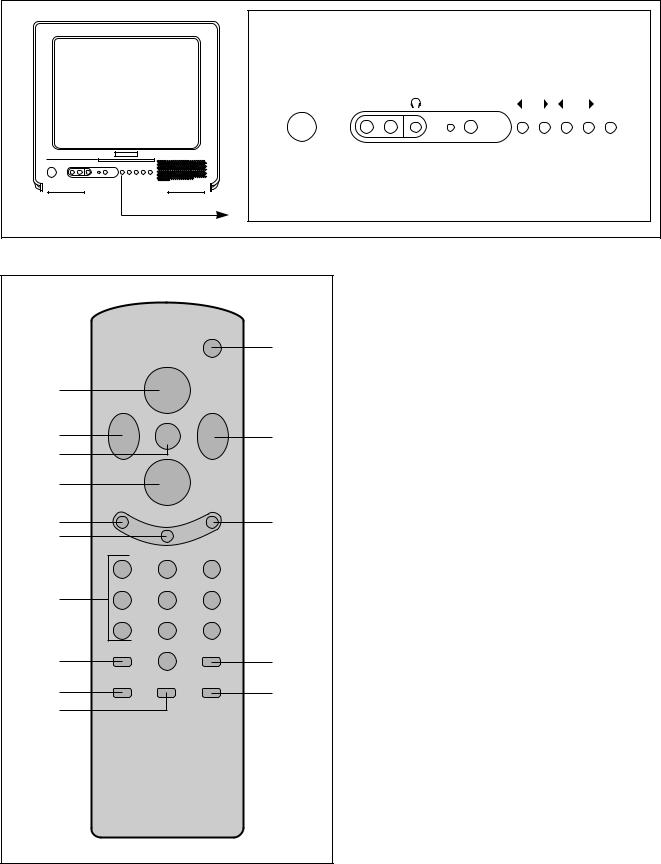
§ LOCATION OF CONTROLS
MAINPOWER |
VIDEO AUDIO |
STAND-BY |
CH |
VOL |
MENU |
§ REMOTE CONTROL UNIT
|
|
|
POWER |
|
|
|
|
|
1 |
2 |
|
CH |
|
|
|
¡ª |
|
|
|
|
|
|
|
|
3 |
VOL |
MENU |
VOL |
3 |
¢‚ |
¢” |
|||
3 |
|
|
|
|
2 |
|
CH |
|
|
|
¡ |
|
|
|
|
RECALL |
|
MUTE |
|
5 |
|
ADD/ERA |
|
7 |
|
|
|
||
6 |
|
|
|
|
1 2 3
8 4 5 6
7 |
8 |
9 |
SLEEP |
|
PREV.CH |
9 |
0 |
10 |
TV/VIDEO |
AUTO.PICT |
AIR/CABLE |
13 |
|
12 |
11 |
|
|
REMOTE CONTROLLER R-25C
1. POWER
Used to turn TV ON or OFF.
2. ¡ªCH¡Â
Use these buttons to change channels on your TV, or select items in the menu system.
3. ¢‚VOL¢”
Use these buttons to change your TV’s volume, to activate selections in the menu system, or to change audio and video settings.
4. MENU
Use this button to turn TV’s menu system on and off.
5. RECALL
Press this button to display the channel number
6. ADD/ERA
Use this button to add a channel to the TV’s memory or erase the channel from memory.
7. MUTE
Use to turn the TV’s sound on and off.
8. 0-9
Use these buttons to change channels.
9. SLEEP
Use this button to program the TV to turn off after a certain time.
10. PREV.CH
Press this button to return to the previous channel you were watching.
11. AUTO.PICT.
Press this button to return TV’s video settings to their original level.
12. AIR/CABLE
Use the button to set up your TV to receive signals from an antenna (AIR) or a cable system (CABLE)
13. TV/VIDEO
Use the button to seiect TV or VIDEO mode.
5

§ GENERAL ALIGNMENT INSTRUCTIONS
THIS RECEIVER IS TRANSISTORIZED. SPECIAL CARE MUST BE TAKEN WHEN SERVICING. READ THE FOLLOWING NOTES BEFORE ATTEMPTING ALIGNMENT.
•Alignment requires an exact procedure and should be undertaken only when necessary.
•The test equipment specified or its equivalent is required to perform the alignment properly.The use of a equipment which does not meet these requirements may result in improper alignment.
•Correct matching of the equipment is essential. Failure to proper matching will result in responses which cannot represent the true operation of the receiver.
•The AC Power line voltage should be kept within from 110 to 220 volts while alignment.
•Do not attempt to connect or disconnect any wire while the receiver is in operation. Make sure the power cord is disconnected before replacing any parts in the receiver.
TEST EQUIPMENTS. |
|
DC POWER SUPPLY ¡ƒ¡ƒ¡ƒ¡ƒ¡ƒ¡ƒ¡ƒ¡ƒ¡ƒ¡ƒ¡ƒ¡ƒ¡ƒ¡ƒ¡ƒ¡ƒ¡ƒ¡ƒ¡ƒ |
0V~30V/500mA Class. |
RF PATTERN GENERATOR¡ƒ¡ƒ¡ƒ¡ƒ¡ƒ¡ƒ¡ƒ¡ƒ¡ƒ¡ƒ¡ƒ¡ƒ¡ƒ¡ƒ¡ƒ¡ƒ¡ƒ |
PHILIPS PM-5518 |
DIGITAL MULTI METER ¡ƒ¡ƒ¡ƒ¡ƒ¡ƒ¡ƒ¡ƒ¡ƒ¡ƒ¡ƒ¡ƒ¡ƒ¡ƒ¡ƒ¡ƒ¡ƒ¡ƒ¡ƒ |
FLUKE 8050A |
WHITE BALANCE TESTER ¡ƒ¡ƒ¡ƒ¡ƒ¡ƒ¡ƒ¡ƒ¡ƒ¡ƒ¡ƒ¡ƒ¡ƒ¡ƒ¡ƒ¡ƒ¡ƒ¡ƒ |
NITSUKI 2840 |
6

§ PIF VCO ADJUSTMENT
[Measuring Instrument Connection]
RF PATTERN |
|
DIGITAL MULTI |
|
|
DC POWER |
|||||||
GENERATOR |
|
|
METER |
|
|
SUPPLY |
||||||
PM-5518 |
|
|
|
|
|
|
|
|
|
|
||
|
|
|
|
|
|
|
|
|
|
|
|
|
|
|
|
|
|
|
|
|
|
|
|
|
|
|
|
|
|
|
|
|
|
|
|
|
|
|
|
|
|
|
|
|
|
|
|
|
|
|
|
|
|
|
|
|
|
|
|
|
|
|
|
|
|
|
|
|
|
|
|
|
|
|
|
|
|
TP1 |
TP3 |
TP4 |
TP5 |
(L102) |
(I501 #7) |
(R701) |
(I201) |
[ADJUSTMENT SET]
(FIGURE 1)
1.Connect the 12V DC POWER SUPPLY to TP4 and TP5.
2.Set the frequency of RF PATTERN GENERATOR with COLOR BAR PATTERN signal to 45.75MHz, and connect the RF output to TP1.
3.Connect the DIGITAL MULTI METER to TP3.
4.Adjust L506 so that the voltage of TP3 becomes 3.8V ± 0.1 Vdc within two DROP-POINTs (FIGURE 2).
V |
adjust point |
3.8V |
core(L506) rotating
voltage drop points (FIGURE 2)
§ SCREEN ADJUSTMENT
1.Push the 9D.SCR key of SERVICE REMOCON to obtain one line picture of screen.
2.Adjust the R,G,B Bias volume in order that the one line of screen may become white color.
7

3.Adjust the SCREEN VOLUME of FBT in order that the one line of screen disappear.
4.Push the 9D.SCR key of SERVICE REMOCON again.
§ FOCUS ADJUSTMENT
1.Receive the RETMA pattern.
2.Adjust the FOCUS volume of FBT to obtain the most clear picture.
§ RF AGC ADJUSTMENT
1.Input the COLOR BAR SIGNAL of 65dB to the ANTENNA INPUT of TV SET
2.Set the user control to AUTO PICTURE ON.
3.Turn completely the RF AGC volume R101 counter-clockwise and turn it clockwise until AGC voltage 6.0V is obtained.
4.If there is the BEAT with strong signal(95 dB over), re-adjust it.
§ VERTICAL CENTER ADJUSTMENT
1. Receive the RETMA PATTERN.
3.Set the user control to AUTO PICTURE ON.
4.Adjust the R302 so that the horizontal center of the PATTERN may meet with the mechanical center of CRT.
§ HORIZONTAL CENTER ADJUSTMENT
1.Receive the RETMA PATTERN.
2.Set the user control to AUTO PICTURE ON.
3. Adjust the R501 in order that the circle may put in the center position of the screen.
|
4 |
|
|
4 |
|
|
1 |
|
|
1 |
|
5 |
3 |
1 |
1 |
3 |
5 |
|
1 |
|
|
1 |
|
|
4 |
|
|
4 |
|
(FIGURE 3) VERTICAL and HORIZONTAL center Adjustmemt
8
§ VERTICAL HIGHT ADJUSTMENT
1.Receive the RETMA PATTERN.
2.Set the user control to AUTO PICTURE ON.
3.Adjust the R301 so that the CENTER of circumference of big circle may meet with the upper and lower sides of screen.
|
4 |
|
|
4 |
|
|
1 |
|
|
1 |
|
5 |
3 |
1 |
1 |
3 |
5 |
|
1 |
|
|
1 |
|
|
4 |
|
|
4 |
|
§ WHITE BALANCE ADJUSTMENT
1.Execute HEAT RUN of the TV SET over 30 minutes with SERVICE REMOCON.
2.Connect the signal output of WHITE BALANCE TESTER (Nitsuki 2840) to the ANTENNA (or VIDEO IN) input of the TV SET. Stick and fix the SENSOR to the center position of CRT.
3.Adjust the R,G,B BIAS and G,B DRIVE VOLUME in order that R,G,B of the HIGH and LOW BEAM may meet with the CENTER LED of each measuring instrument.
4.At this time, the memorized coordinates of the WHITE BALANCE TESTER, unless otherwise specified, use
following coordinates and color temperature (PAL:9600K 3~5ftL 265¡¿295 , NTSC: 10850K 3~5ftL 274¡¿289)
§ SUB-BRIGHT ADJUSTMENT
1.Receive the RETMA PATTERN.
2.Set the user control to AUTO PICTURE ON.
3.Turn the SUB-BRIGHT CONTROL VOLUME (R540) and adjust the gradation pattern as shown.
4.The status that the border between 15% and 20% can be distinguished.
9
§DESCRIPTION OF CIRCUIT OPERATION
§FEATURE OF THE CM-537
•VIDEO, CHROMA, DEFLECTION in one-chip IC. •Automatic switching of 3-SYSTEM(NTSC, PAL-M, PAL-N). •FS(Frequency Synthesizer ) Tunning System.
•Function of LAST MEMORY against the electric failure (E2PROM:24LC028). •Separation of PIF and SIF(SAW filter :DSW1013P)
•Minimization of Ringing by applying Ringing-less FBT(2001SPND)
•Auto-compensation of the vertical height level against the frequency change of AC power . •OVER CURRENT PROTECTION Circuit.
•Elimination Circuit of POP NOISE.
§ OPERATION CHARACTERISTICS OF EACH BLOCK
A.¥-COM BLOCK
1. ¥-COM(DMC42C522N, I701) PIN DESCRIPTION/OPERATION
PIN |
NAME/(ABBREV) |
FUNCTION |
REMARK |
|
|
|
|
1 |
NTSC-M |
3-SYSTEM SWITCHING |
CMOS |
|
(RCO/PWM14) |
|
PUSH PULL |
|
|
|
|
2 |
PAL-M |
3-SYSTEM SWITCHING |
CMOS |
|
(R83) |
|
PUSH PULL |
|
|
|
|
3 |
AC POWER DOWN |
MAIN POWER DOWN Detect input:active LOW |
CMOS |
|
(R03/INT3) |
|
PUSH PULL |
|
|
|
|
4 |
SD INPUT |
SYNC. signal INPUT H: signal detect |
|
|
(RO2/INT2) |
L: no signal |
|
|
|
|
|
5 |
REMOTE CONTROL |
REMOTE CONTROL signal input |
|
|
INPUT |
REMOTE CONTROL IC : M50560-388GP/M50560-001 |
|
|
(R01/INT1TIM1) |
(CUSTOM CODE: 14H) |
|
|
|
|
|
6 |
KEY RETURN IN 0 |
·KEY MATRIX COLUMN 0 |
|
|
(R00/INT0/TIM0) |
·HOLD MODE : WAKE-UP using INT1 |
PUSH PULL |
|
|
|
|
7 |
Xin |
SYSTEM CLOCK : 4.1943 MHz |
|
8 |
Xout |
|
|
|
|
|
|
9 |
RESET |
SYSTEM RESET |
|
|
|
|
|
10 |
KEY RETURN IN 1 |
KEY MATRIX COLUMN 1 |
|
|
(R82) |
|
|
|
|
|
|
11 |
Vss |
GND |
|
|
|
|
|
12 |
KEY RETURN IN 2 |
KEY MATRIX COLUMN 2 |
|
|
(R81) |
|
|
|
|
|
|
13 |
KEY SCAN OUT 0 |
· KEY MATRIX ROW 0 |
|
|
& TIMER |
· Active HIGH when ON TIMER is set. |
|
|
(R80) |
|
|
|
|
|
|
10
PIN |
NAME/(ABBREV) |
FUNCTION |
REMARK |
|
|
|
|
14 |
Vdd |
+5V |
|
|
|
|
|
15 |
KEY SCAN OUT 1 |
· KEY MATRIX COLUMN 1 |
|
|
& CLOCK |
· TUNER CLOCK & EEPROM CLOCK |
|
|
(R23) |
|
|
|
|
|
|
16 |
KEY SCAN OUT 2 |
· KEY MATRIX COLUMN 2 |
|
|
& DATA |
· TUNER DATA & EEPROM DATA |
|
|
(R22) |
|
|
|
|
|
|
17 |
ENABLE |
· TUNER ENABLE |
CMOS |
|
(R20/PCL) |
|
PUSH PULL |
|
|
|
|
18 |
AFC |
· AFC voltage from MAIN IC(LA7688) : DC 0 ~Vdd |
A/D CONV |
|
(R21/AFC IN) |
CENTER : 2.5V |
4BIT |
|
|
|
|
19 |
OSC in |
· OSD CLOCK |
|
|
|
|
|
20 |
OSC out |
|
|
|
|
||
|
|
|
|
21 |
/H-Sync |
· SYNC. signal for OSD H. position. |
|
|
(HD) |
· 0~5V PULSE/Active LOW INPUT |
|
|
|
|
|
22 |
/V-Sync |
· SYNC. signal for OSD V. position. |
|
|
(VD) |
· 0~5V PULSE/Active LOW INPUT |
|
|
|
|
|
23 |
R(R60/OSD R) |
· Active “HIGH” OUTPUT |
|
|
|
|
|
24 |
G(R61/OSD G) |
· Dot pattern OF OSD |
|
|
|
|
|
25 |
B(OSD B) |
|
|
|
|
|
|
26 |
OSD Ys |
|
|
|
|
|
|
27 |
50/60 IN |
· 3-SYSTEM SWITCHING |
CMOS |
|
(R13) |
· 50Hz: LOW(PAL-N) , 60Hz: HIGH (PAL-M, NTSC-M) |
|
|
|
|
|
28 |
/C.IDENT IN |
· 3-SYSTEM SWITCHING |
CMOS |
|
(R12) |
· “LOW” (INPUT) signal detected with NO-COLOR. |
|
|
|
|
|
29 |
OCP IN |
· OVER CURRENT PROTECTION INPUT: active HIGH |
CMOS |
|
(R11) |
· TV POWER turns OFF when HIGH signal detected for |
|
|
|
10ms. |
|
|
|
· The u-COM observe this pin immediately after |
|
|
|
POWER ON. |
|
|
|
|
|
30 |
SCREEN OUT |
· HIGH signal OUTPUT indicating SCREEN adjustment. |
CMOS |
|
(R10) |
· Goes HIGH when REMOCON KEY;9DH detected. |
|
|
|
· Toggled when 9DH detected. |
|
|
|
|
|
31 |
VIDEO MUTE OUT |
· Active LOW, Normal : HIGH |
CMOS |
|
|
|
|
11
PIN |
NAME/(ABBREV) |
|
FUNCTION |
REMARK |
|
|
|
|
|
32 |
POWER |
· Active HIGH |
|
|
|
|
· LOW state at initial condition (RESET). |
except |
|
|
|
· Toggle LOW/HIGH when POWER KEY input is detected. |
HEAT-RUN mode |
|
|
|
(LOW ¡ POWER OFF / HIGH ¡ POWER ON) |
|
|
|
|
· Automatically turns to LOW when SLEEP TIMER |
|
|
|
|
(count down) counts “0”. |
|
|
|
|
· Automatically turns to LOW when the OFF TIMER is set |
|
|
|
|
and the clock(TV) indicates OFF-TIME. |
|
|
|
|
· Automatically turns to HIGH when the ON TIMER is set |
|
|
|
|
and the clock (TV) indicates ON-TIME. |
|
|
|
|
|
|
|
33 |
TV/VIDEO |
· TV: HIGH / VIDEO: LOW |
CMOS |
|
|
(R31) |
· VIDEO MUTE(#31) is activated for a moment |
PUSH PULL |
|
|
|
when this pin is togglled. |
|
|
|
|
(VIDEO MUTE MODE needs OPTION diodes) |
|
|
|
|
|
|
|
34 |
SOUND MUTE |
· Active HIGH, Normal : LOW |
CMOS |
|
|
(R30) |
· HIGH out ¡ MUTE. |
PUSH PULL |
|
|
|
· Following action make the TV set to be MUTE |
|
|
|
|
for a moment. |
|
|
|
|
1. |
Channel selecting |
|
|
|
|
direct selecting, sequential channel selecting, |
|
|
|
|
AUTO PROGRAM |
|
|
|
2. |
POWER ON/OFF |
|
|
|
· When MUTE KEY is detected following changes |
|
|
|
|
are occurred for a moment. |
|
|
|
|
1. VOLUME level ¡ LOW |
|
|
|
|
2. SOUND MUTE(#34) ¡ HIGH |
|
|
|
|
3. Color of OSD : GREEN ¡ RED |
|
|
|
|
|
|
|
35 |
VOLUME |
· Active HIGH, PWM OUTPUT |
CMOS |
|
|
(PWM82) |
· 64 STEP (2bit/step) VOLUME CONTROL |
|
|
|
|
· Following action make the VOLUME level to “0” |
|
|
|
|
(MUTE) for a moment. |
|
|
|
|
1. Channel selecting |
|
|
|
|
2. TV/VIDEO selecting |
|
|
|
|
|
|
|
36 |
BRIGHTNESS |
· Active HIGH, PWM OUTPUT |
|
|
|
(PWM81) |
· 64 step (2bit/step) BRIGHTNESS CONTROL |
|
|
|
|
|
|
|
37 |
CONTRAST |
· Active HIGH, PWM OUTPUT |
|
|
|
(PWM80) |
· 64 step (2bit/step) CONTRAST CONTROL |
|
|
|
|
|
|
|
38 |
SHARPNESS |
· Active HIGH, PWM OUTPUT |
|
|
|
(RC3/PWM63) |
· 64 step (2bit/step) SHARPNESS CONTROL |
|
|
|
|
|
|
|
39 |
COLOR |
· Active HIGH, PWM OUTPUT |
|
|
|
(RC2/PWM62) |
· 64 step (2bit/step) COLOR CONTROL |
|
|
|
|
|
|
|
40 |
TINT |
· Active HIGH, PWM OUTPUT |
|
|
|
(RC3/PWM63) |
· 64 step (2bit/step) TINT CONTROL |
|
|
|
|
|
|
|
2.Function of LAST MEMORY
Always holds a previous DATA by saving the signal of the data,clock,enable on the E2PROM.
12

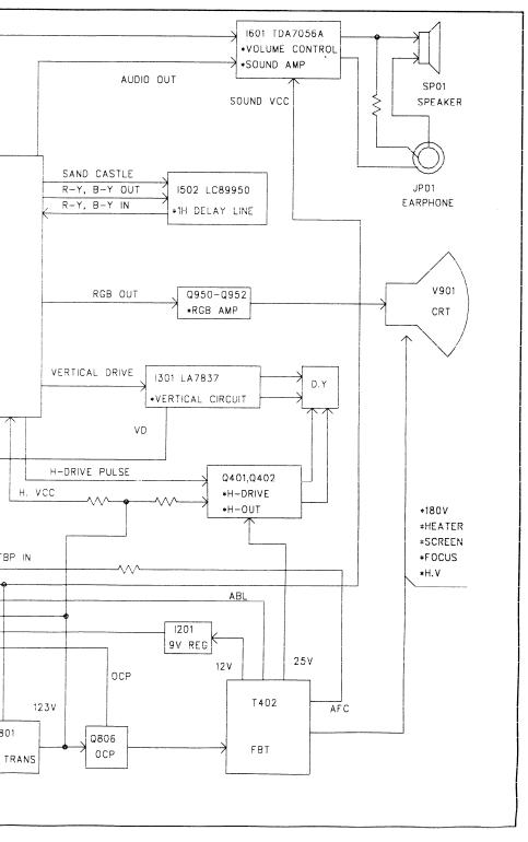
B. VIDEO BLOCK
1.TV/VIDEO SWITCHING
1)SWITCHING BLOCK DIAGRAM
µ-COM |
I501 |
|
|
LA7688 |
|
|
|
(I701) |
|
9V |
|
|
|
||
|
VIDEO |
8 |
Q503 |
TV(H) 33 |
DET |
||
1 |
|
|
|
/VI(L) |
VIDEO |
|
|
|
|
|
|
|
SWITCH |
|
|
SIF |
|
10 |
|
Filter |
|
|
|
|
|
14 |
EXT.VIDEO |
|
|
(JV01/JV02) |
R,G,B OUT
2) CIRCUIT OPERATION
•After going out to the #8 of I501, the detected signals go into the #10 of I501through 4.5MHz BPF(Band Pass Filter, Z502) : TV SIGNAL.
•The external VIDEO signals from JV01(or JV02) go into the #14 of I501 : VIDEO SIGNAL.
•Output pulse from the #33 of the ¥-COM(TV:HIGH, VIDEO:LOW) go into #1 of I501 through a buffer(Q504 and Q507).
•According to the input pulse of the #1, TV/VIDEO switching circuit let out the video signals to the RGB generator block inside I501.
2.OUTLINE AND OPERATION OF 3-SYSTEM AUTO SWITCHING
1)SWITCHING BLOCK DIAGRAM
I701 |
|
|
|
I501 |
µ-COM |
|
|
|
LA7685J |
NTSC-M |
1 |
X502 |
|
|
|
|
|
||
|
|
X503 |
41 |
VCO |
|
2 |
|
|
|
PAL-M |
|
|
|
|
|
7.6V |
X501 |
|
|
|
|
|
|
|
|
Q506 |
9V |
|
|
|
|
|
|
27 |
21 |
50/60 |
|
Q502 |
|
||
|
9V |
|
|
28 |
R766 |
|
|
17 COLOR |
|||
|
|||
R774 |
Q705 |
/KILLER |
|
|
|
||
2) CIRCUIT OPERATION
•If 50[Hz] detected. #21 of the I501 goes down to LOW level. This out goes into the Q506 (and #27 of the I701), and then X501 oscillates (#1 and #2 of the I701 are deactivated.).
13

¢¡PAL-N system
•If 60[Hz] detected, #21 of the I501 goes up to HIGH level and the system operates as PAL-M or NTSC-M.
¤ In the case that Base voltage of Q705 is LOW, the voltage driven from R766 and R774 is applied to the #28 of the I701.
¤ŁIn the case that Base voltage of Q705 is HIGH, according to the voltage change of the #28 of the I701, the comparator in the I701 switch over the system.
(PAL-M¢¡NTSC-M, NTSC-M¢¡PAL-M)
•HIGH signal of the #1 of I701 makes X502 oscillates.(NTSC-M) •HIGH signal of the #2 of I701 makes X503 oscillates.(PAL-M)
3) FREQUENCY CHARACTERISTICS OF EACH SYSTEM
|
|
|
SCANNING |
LINE |
FIELD |
CHROMINANCE |
|
COLOR |
VHF |
UHF |
FREQUENCY |
SUB CARRIER |
|||
NUMBER |
FREQUENCY |
||||||
|
|
|
(Fh) |
(Fsc) |
|||
|
|
|
|
|
|||
NTSC |
M |
M |
525line |
15,734[Hz] |
60[Hz] |
3.579545[MHz] |
|
|
|
|
|
|
|
|
|
PAL |
M |
M |
525line |
15,734[Hz] |
60[Hz] |
3.575611[MHz] |
|
|
|
|
|
|
|
|
|
PAL |
M |
|
625line |
15,625[Hz] |
50[Hz] |
3.582056[MHz] |
|
|
|
|
|
|
|
|
C. SOUND BLOCK
1. SOUND BLOCK DIAGRAM
|
|
I501 |
|
|
|
|
LA7688 |
|
|
|
SIF |
FM |
|
|
|
DET |
|
|
|
|
|
|
|
|
|
|
AUDIO |
|
I601 |
|
|
|
TDA7056A |
|
|
|
SWITCH |
|
|
|
|
|
6 |
|
|
|
|
|
|
|
|
51 |
3 |
SP |
|
|
|
||
EXT. |
|
12 |
|
8 |
AUDIO |
|
|
||
(JV01/JV02) |
|
|
|
|
|
|
|
from the µ-COM(#33) |
|
2.EXPLANATION OF OPERATION
1)The TV audio signal is detected and goes into the audio switch in I501.
2)The external audio signal from JV01(or JV02) goes into the #12 of I501.
3)The audio switch in I501 alternates audio signals according to the TV/VIDEO control input from the I701.
4)The selected audio signal (#51 of I501) go into the #3 of I601.
14
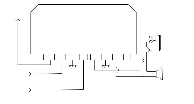
3.SOUND AMP IC
1) BLOCK DIAGRAM
33V |
|
|
|
|
|
|
|
|
|
|
|
TDA7056A |
|
|
|
||
|
|
|
|
|
|
|
|
Earphone |
|
|
|
|
|
|
|
|
Jack |
N.C |
VP |
IN |
S.GND Volume OUT(+) P.GND OUT(–) |
N.C |
||||
1 |
2 |
3 |
4 |
5 |
6 |
7 |
8 |
9 |
From |
|
|
|
|
|
|
|
SPEAKER |
#51 |
|
|
|
|
|
|
|
16 ohm |
of I501 |
|
|
|
|
|
|
|
3W |
From |
|
|
|
|
|
|
|
SP01 |
|
|
|
|
|
|
|
|
|
#35 |
|
|
|
|
|
|
|
|
of I701 |
|
|
|
|
|
|
|
|
2) EXPLAINATION OF THE OPERATION
•The audio signal from the I501 goes into the #3 of the I601.
•I601 amplifies this audio signal correspond to the volume control signal from I701. •The amplified audio signal from the #6 and #8 drives the speaker (s).
¡ AUDIO MUTE function is activated by the I701(SOFTWARE MUTE).
15

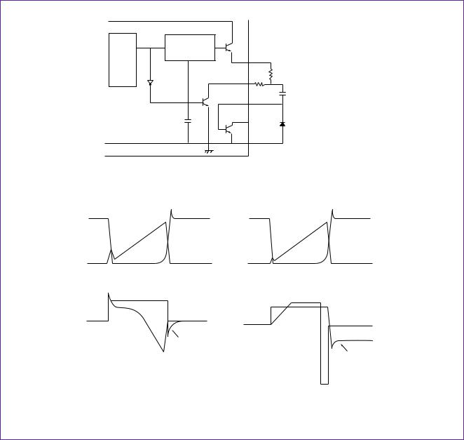
D. DEFLECTION BLOCK
This block can be separated into two parts, VERTICAL and HORIZONTAL. Only the VERTICAL circuit is explained here, comprehensibly.
1. BLOCK DIAGRAM OF VERTICAL IC
|
|
|
|
|
|
LA7837 |
|
|
|
|
||
|
|
|
|
|
|
|
|
THERMAL PROTECTION |
|
|
||
|
|
|
Ramp |
|
|
|
|
|
|
|
|
|
|
|
|
Generator |
|
|
Vert. Drive |
|
Vert. Out |
|
|||
Vert. |
One |
|
Vert. |
|
|
|
|
|
|
|
|
|
Trig. |
Shot |
|
Size |
|
|
Pump UP |
|
|
|
|
||
Input |
Multi |
|
Control |
|
|
|
|
|
|
|
|
|
|
|
|
|
S.W |
|
|
|
|
|
|
|
|
1 |
2 |
3 |
4 |
5 |
6 |
7 |
8 |
9 |
10 |
11 |
12 |
13 |
+B1 |
|
|
|
|
|
+B7 |
|
|
|
|
|
|
|
|
|
|
|
|
|
|
|
|
|
|
|
9V |
+ |
|
|
|
|
25V |
|
+ |
10~20P |
|
|
|
|
|
|
|
|
|
|
|
|
|
|||
|
|
|
|
50/60 |
|
|
|
|
|
|
DY |
|
|
|
|
|
Hz |
|
|
|
|
|
+ |
+ |
|
|
|
|
|
|
|
|
|
|
|
|
|
|
|
VERT. |
|
|
Vert. Height. |
|
|
|
|
|
|
||
|
TR1G. |
|
|
|
|
|
|
|
|
|||
|
|
|
|
|
|
|
|
|
|
|
|
|
|
1N |
|
|
|
|
|
|
|
|
|
|
|
|
|
|
|
|
|
|
|
|
|
vert |
|
|
|
|
|
|
|
|
|
|
|
|
center |
|
|
# 1: B+ (12V) |
# 8: POWER SUPPLY (VBB): 25V |
# 2: VERTICAL TRIGGER INPUT |
# 9:PUMP UP OUTPUT |
# 3: TIME CONSTANT & MUTE |
#10:OSC BLOCKING |
# 4: VERTICAL HEIGHT CONTROL |
#11:GND |
# 5: 50/60[Hz] VERTICAL SIZE CONTROL SIGNAL |
#12:VERTICAL OUTPUT |
INPUT |
#13:POWER SUPPLY FOR VERTICAL OUTPUT |
# 6: RAMP WAVEFORM GENERATION |
|
# 7: AC/DC FEEDBACK INPUT TO VERTICAL |
|
16

2. OPERATION OF VERTICAL
(a)
VCC
|
GND |
|
|
|
(b) Q3 Collector |
|
|
Current i1 |
Q3 |
i1 VCC1 |
|
|
|
|
|
GND |
|
|
|
(c) Q4 Collector |
|
|
Current i2 |
Q4 |
|
|
|
GND |
|
|
|
(d) Current of |
Q2 |
|
Deflection coil |
|
i1 + i2 |
|
|
i2 |
|
|
|
|
|
VCC |
(e)Emitter Voltage |
|
1/2 VCC |
|
|
GND |
|
VERTICAL OUTPUT WAVE
1)In the picture above, (a) shows a fixed Vcc, and (+)(-)current of deflection coil is (d) whichk is sum of (b) and (c), and (e) shows EMITTER voltage of Q3,Q4.
2)Collector loss of Q3 is i1 Vce1 which is the product of obligue region of (b),(e).Collector loss of Q4 is product of dot region of (c),(e).
3)To reduce collector loss of Q3,if bring down the voltage during scanning time as shown in the picture (b) , Vce1 become lower so that the loss diminish.
Diminish if Q3 Collector Loss
Blanking Time
Voltage
Sanning Time
Voltage
OUTPUT VOLTAGE
17

E. POWER BLOCK
This chassis designed for free voltage(AC 100V ~ AC 220V ) power. power block contains power IC, SMPS transformer and several passive components.
The power IC STR-S5707 has power transistor. oscillator circuit, voltage comparator circuit, thermal protection circuit, OCP(over current protection) circuit insiude.
1.STR-S5707 BLOCK DIAGRAM
V IN
|
|
|
|
9 |
|
|
|
|
|
|
|
|
|
|
|
|
START UP |
OVP |
LATCH |
|
|
|
Tr2 |
8 |
DIRVE |
|
|
|
|
|
|
PROPOTIONAL |
||||||
|
|
|
|
|
|
|
|
|
DRIVE |
R3 |
|
|
|
|
|
|
|
|
|
|
|
|
|
|
|
SENS |
7 |
|
PNP +2Di |
PRE REG |
|
OSC |
|
|
|
R4 |
4 |
SINK |
|
|
|
|
|
|
|
||||||
|
|
|
|
|
|
|
|
|
OCP |
|
3 |
B |
|
R6 |
|
|
T.S.D |
|
|
INH-1 |
|
REF |
|
1 |
C |
|
|
|
|
|
|
|
Tr1 |
|||||
|
|
|
R1 |
|
|
|
|
|
||||
|
|
|
|
|
|
|
REF |
|
|
|
|
|
|
|
|
|
|
|
|
|
|
|
|
|
|
|
|
|
|
|
|
|
INH-2 |
|
|
|
|
|
|
|
|
|
|
|
|
|
REF |
|
|
|
|
|
R7 |
R8 |
R9 |
|
|
|
INH-3 |
|
|
|
2 |
GND |
|
|
|
|
|
|
|
|
REF |
|
R4 |
|
|
|
|
|
|
|
|
|
|
|
|
5 |
OCP |
|
|
|
|
|
|
|
|
|
|
|
|
||
|
|
|
|
|
C1 |
R2 |
C2 |
C4 |
R5 |
C3 |
|
|
|
|
|
|
|
|
|
|
|
6 |
|
|
|
|
|
|
|
|
|
|
|
|
INH |
|
|
|
2.PIN DESCRIPTION
PIN NO |
SYMBOL |
NAME |
|
FUNCTION |
|||
1 |
|
C |
|
COLLECTOR |
POWER TRANSISTOR COLLECTOR |
||
|
|
|
|
|
|
|
|
2 |
|
GND |
|
GROUND |
GROUND(POWER TRANSISTOR EMITTER) |
||
|
|
|
|
|
|
|
|
3 |
|
B |
|
BASE |
POWER TRANSISTOR BASE |
||
|
|
|
|
|
|
|
|
4 |
|
SINK |
|
SINK |
BASE CURRENT (Is) INPUT |
||
|
|
|
|
|
|
|
|
5 |
|
OCP |
|
OVER CURRENT PROTECTION |
OVERCURRENT SENSING SIGNAL INPUT |
||
|
|
|
|
|
|
|
|
6 |
|
INH |
|
INHIBIT / LATCH |
SYNC, OFF TIME/LATCH CIRCUIT CONTROL INPUT |
||
|
|
|
|
|
|
|
|
7 |
|
F/B(SENS) |
FEED BACK(SENSING) INPUT |
CONSTANT VOLTAGE CONTROL SIGNAL INPUT |
|||
|
|
|
|
|
|
|
|
8 |
|
DRIVE |
|
DRIVE |
BASE DRIVE CURRENT (Id) OUTPUT |
||
|
|
|
|
|
|
|
|
9 |
|
Vin |
|
Vin |
SUPPLY VOLTAGR FOR CONTROL CIRCUIT |
||
|
|
|
|
|
|
||
3. OTHER FUNCTION |
|
|
|||||
|
|
|
|
|
|
|
|
|
Symbol |
|
Function |
|
|
||
|
OVP |
|
Built-in Overvoltage Protection Circuit |
|
|
||
|
|
|
|
|
|
|
|
|
TSD |
|
Built-in Thermal Shutdown Circuit |
|
|
||
|
|
|
|
|
|
|
|
18
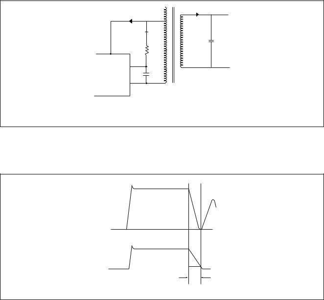
4. EXPLAINATION OF CIRCUIT OPERATION
1) VIN terminal, start-up circuit
A start-up circuit is to start and stop a operation of a control IC by detecting a voltage appearing at a VIN terminal (pin-9). At start up of a power supply, when a voltage at the VIN terminal reaches to 8V by charging up C806 by the function of a start-up resistor, Rs, a control circuit starts operating by the function of the start-up circuit. As shown in Fig. 2, since a circuit current is suppressed 200§¸ maximum ( at VIN = 7.5V ) until the control circuit starts its operation.
After the control circuit starts its operation, power source is obtained by smoothing voltage appearing at L1 winding. Once the control circuit starts operating, as its voltage doesn’t reach the fixed voltage at once, VIN terminal voltage starts dropping. However, as a shut-down voltage is set low (at 4.9V), while VIN terminal voltage reaches a shutdown voltage, L1 winding voltage reaches the fixed voltage earlier so that the control circuit can continue on operating.
AC |
|
|
IN |
|
IN |
Rs(R803,R804) |
Ln |
20mA |
|
|
|
|
||
1 |
9 |
D804 |
|
|
|
|
|
||
|
VIN |
L1 |
|
|
|
C806 |
200µA |
|
|
|
2 |
|
4.9V 7.5V 8V |
Vin |
|
GND |
|
||
|
Fig .1 Start-up Circuit |
|
Fig .2 VIN Terminal Voltage Circuit Current VIN |
|
2) Osciliator, F/B terminal voltage (Pin #7)
A oscillator generates pulse signals which turns a power transistor on and off by making use of charge and discharge of CI and C2 incorporated in the Hybrid IC.
Constant voltage control of a switch-mode power supply is performed by changing both ONtime and OFFtime except when the load is light (ex. remote control stand-by mode of TVs).
Fig. 4 shows how the oscillator works when the Hybrid IC independently operates (with no F/B nor INH signals). When the power thransistor is on, C2 Is charged to the set voltage (approx 2.3V at Ta =25°C). On the other hand, C1 starts charging up through R1 from almost 0V and the voltage across C1 increases in accordance with the inclination determined by the product of C1 and R1. When the voltage across C1 reaches approx. 0.75V (Tc=25°C). the output from the oscillator is reversed and the power transistor turns off. At the same time C1 is quickly discharged by the function of a internal circuit of the oscillator and the voltage across it decreases to almost 0V. When the power transistor turns off, C2 starts discharging through R2 and the voltage across C2 decreases in accordance with the inclination derermined by the product of C2 decreases to about 1V. the output from the oscillator is reversed again and the transistor consequently turns on. The power transistor continues turning on and off by repeating the above-mentioned operations.
19

|
L1 |
|
2.3V |
|
|
2.3V |
|
|
|
C2 ACROSS |
|
|
|
C2 ACROSS |
|
Reg |
|
Voltage |
|
|
Voltage |
||
|
|
1V |
|
|
|
1V |
|
|
|
|
R7 |
PIN +2Di |
R6 |
|
R1
OSD
Drive
Cfrcu1
+ |
INH |
0.75V |
0.75V |
COMP 1 |
Tre |
C1 ACROSS |
|
– |
|
C1 ACROSS |
|
+ |
VTH1 |
Voltage |
|
|
Voltage |
||
|
0V |
||
COMP 2 |
|
0V |
|
– |
VTH2 |
|
R7 R8 R9
|
|
Osc. |
|
|
Osc. |
|
C1 C2 |
R2 |
Output |
|
|
Output |
|
|
|
PTR |
0V |
ON |
PTR |
0V |
|
OFF |
|
Fig 3 Oscillator Circuit Configulation |
Fig 4 Operation Waveforms of Oscillator without F/B nor |
Fig 5 Operation Waveforms of Oscillator with F/B Signal |
|
INH Signal |
|
As the circuit in Fig. 3 shows, the ON-time is controlled by changing a current charged by C1, which is as the result of that the detection winding (L1),which detects a change of voltage in a secondary side, connected to the sensing terminal (Pin No. 7) has the current in accordance with an output signal from an output voltage detection circuit (an error amplifier) built in. As an AC input voltage to the power supply gets the higher and a load current the smaller, the current flowing to the SENS terminal gets the larger, and the ON-time gets the shorter.
3) Function of INH terminal (Pin #6), control of OFF-time
Signal to the INH terminal is used as inputs to COMP.1 and COMP.2 inside of the control IC. A threshold voltage of COMP.1 VTH1 is set at 0.75V (Ta=25°C) and an input signal to a drive circuit becomes almost 0V (the power transistor is in OFF mode) when a voltage at the INH terminal reaches the VTH1. As long as the INH terminal voltage does not get lower than VTH1. the power transistor sustains OFF mode. On the other hand, a threshold voltage of COMP.2 VTH2, is set at 1.5V (Ta=25°C).When the INH terminnal voltage reaches VTH2, an output from COMP.2 reverses and, as a result, C2 starts firing and a voltage across C2 drops to almost 0V in a moment. As the result of this immediate discharge of C2, the OFF-time of the oscillator which has been determined by the product of C2 and R2 (⁄ 55 ¥ sec) can be quicker up to approx. 2¥sec. As long as the INH terminal voltage does not get lower than VTH2, AVoltage across C2 stays at almost 0V and a output from the oscillator keeps the power transistor being on. The relation between the INH terminal voltage and the function of the oscillator described above is shown in Fig. 6 and Fig. 7
Osc.
Output
|
|
|
|
|
|
PTR |
|
|
|
|
|
|
|
|
|
|
|
ON |
OFF |
||
|
|
|
|
|
|
2.3V |
|
|
|
|
|
|
|
|
|
|
C2 ACROSS |
|
|
|
|
Osc. |
|
|
|
|
Voltage |
|
|
|
||
Output |
|
|
|
|
|
|
|
|
|
|
PTR |
|
|
|
|
|
0V |
|
|
|
|
|
ON |
OFF |
|
|
|
|
|
|||
|
|
|
|
|
|
|
||||
INH |
VTH1 |
|
INH |
VTH2 |
|
|
||||
|
|
|
|
|||||||
|
Ter. Voltage. |
|
|
|
||||||
Ter. Voltage |
|
|
|
|
|
|
||||
|
|
|
|
|
|
|
|
|||
|
|
|
|
|
|
|
||||
Fig .6 Operation Waveforms of INH Terminal(VTH1) |
Fig .7 Operation Waveforms of INH Terminal(VTH2) |
|||||||||
20
4) Quasi-resonant operation
By inputting a voltage signal which is synchronized with the energy discharge time of a secondary winding of a transformer to the. INH terminal, quasi-resonant operation can be achieved. As shown in Fig. 8 , the voltage of L1 winding which is synchronized. with the energy discharge time of a secondary winding. S1. shall be input to the INH terminal through D805 and R807. Since VTH2 is set at 1.5V typical, a voltage at the INH terminal. VINH, shall be set at 2V.
D803
 D805
D805
+
S1
R807 L1
9
VIN 6 INH 
2 C808 GND
Fig 8 Operation Circuit
Fig. 9 shows waveforms of VCE, Ic and VINH of the transistor, voltage across C808 in the oscillator as well as an output from the oscillator when operating in quasi-resonant mode.
VCE
0V
INH Terminal
Voltage
VTHI
0V
tr
Fig 9 Waveforms of VCE and VINH at Quasi-resonant Operation
when the power transistor turns off and a voltage higher than VTH2 is applied to the INH terminal, C808 immediately discharges and then starts charging again. Even after the discharge of energy of a secendary winding is completed, VINH does not immediately increases. When it gets lower than VTH2 after the time,tr, which is determined by the production of internal impedance of the IC and CINH, has past, the transistor turns on.
21
5) Drive circuit
The STR-S5707 applies the proportional drive system in order to minimize turn-on and satruration loss, and storage time. In the conventional RCC system, turn-on loss and switching noise due to the surge current appearing when the power transistor turns on are high as because the transistor is driven by the drive current shown in Fig. 10-1. In addition, since is decreases linearly when the transistor turn off and a peak value of IB2 is not large, the storage time is long and the VCE(sat) voltage is high, which results in large turn-off loss. The circuit and the waveforms of the proportional drive system which is applied to the STR-S5707 in order to reduce these switching loss and shorten the storage time are shown in Fig . 10 and Fig. 10-2 respectively.
Drive
OSC
R810
C805
D806
Fig .10 D806 and C805 function to reverse-blas between the base and the emitter of the transistor during its off state.
VCE |
VCE |
IC |
IC |
0 |
0 |
VBE |
VBE |
|
|
IB |
IB |
|
|
Reveres |
|
bias |
Reveres |
|
|
|
bias |
Fig .10-1 Waveforms of Conventional |
Fig .10-2 Waveforms of power Supply |
RCC Power Supply |
Using STR-S5707 |
22
 Loading...