


(without price)
EV-660C (PAL B / G,H)
EV-660I (PAL B / G)
EV-660N (PAL B / G,H)
EV-660D (PAL I)
(KX-637)
SEP. 1999
INDEX
EV-660
Ver.1 Feb / 2000
R
CONTENTS
SPECIFICATIONS ......................................................................................... |
1 |
BLOCK DIAGRAM ....................................................................................... |
2 |
ADJUSTMENTS ............................................................................................ |
3 |
EV-660C/I/N ............................................................................................... |
4 |
EV-660D ..................................................................................................... |
9 |
PRINTED CIRCUIT BOARDS ..................................................................... |
14 |
EXPLODED VIEW ....................................................................................... |
16 |
PARTS LIST ................................................................................................ |
17 |
SCHEMATIC DIAGRAMS ........................................................................... |
19 |
SPECIFICATIONS
|
Item |
|
Specification |
|
|
|
|
1. |
Type |
LCD Color Television |
|
|
|
|
|
2. |
Reception Frequencies |
UHF: UHF band |
CH 21 – CH 69 (models C and N) |
|
|
|
CH 21 – CH 68 (model D) |
|
|
VHF: VHF band |
CH 2 – CH 12 (models C and N) |
|
|
|
|
3. |
Display Element |
High resolution color liquid crystal display (TN Type) |
|
|
|
|
|
4. |
Drive System |
TFT active matrix system |
|
|
|
|
|
5. |
Screen Size |
3 inches |
|
|
|
|
|
6. |
Backlight |
High luminance fluorescent material |
|
|
|
|
|
7. |
Antenna |
Rod antenna (VHF, UHF) |
|
|
|
|
|
8. |
Speaker |
12/16ø inches (28 mm) × 1 |
|
9. |
Connection Terminals |
Earphone jack (3.5ø mini) |
|
|
|
External power source jack (DC IN 6V) |
|
|
|
Audio/Video input jack (3.5ø mini) |
|
|
|
|
|
10. |
Power Supply |
3-way power supply system |
|
|
|
Batteries: |
4 AA-size dry batteries |
|
|
AC: |
AC adaptor AD-K64/AD-K65 (option) |
|
|
Car battery |
Car adaptor CA-K65 (option) |
|
|
|
|
11. |
Power Consumption |
Approx. 3.8 W |
|
|
|
|
|
12. |
Ambient Temperature Range |
32°F (0°C) ~ 104°F (40°C) |
|
|
|
|
|
13. |
Dimensions |
3 7/16" (W) × 1 9/16" (D) × 5 1/16" (H) inches |
|
|
|
87 (W) × 39 (D) × 128 (H) mm |
|
|
|
|
|
14. |
Weight |
Approx. 8.5 oz |
240 g (excluding batteries) |
|
|
|
|
Model |
Color System |
TV System |
|
Channel |
|
|
|
|
|
|
|
EV-660C/N |
PAL |
B/G, H |
CCIR |
VHF: 2 ~ 12 ch |
UHF: 21 ~ 69 ch |
|
|
|
|
|
|
EV-660D |
PAL |
–/I |
UK |
— |
UHF: 21 ~ 68 ch |
|
|
|
|
|
|
EV-660I |
PAL |
B/G |
ITALY |
VHF: A ~ H2 ch |
UHF: 21 ~ 69 ch |
|
|
|
|
|
|
— 1 —

BLOCK DIAGRAM
BATTERY 1.5V x 4
AC ADAPTOR 6V
— 2 —
EXTERNAL VIDEO
EXTERNAL AUDIO
EAR
PHONE
SP
L-PCB
ANT
BT |
|
|
|
TUNER |
PRE |
SAW |
VIF/SIF |
(TEPE5-01) |
AMP |
FILTER |
(M51348FP) |
BS |
BV |
BU |
POWER SW
BAND SW
VCC1-1 |
VIDEO1 |
AUDIO1 |
|
|
VIDEO2
AV JACK
VCC1-1  AUDIO2
AUDIO AMP (NJM2070M)
Vcc7(30V)
Vcc6(18.5V)
DC/DC Vcc5(12V)
CONVERTER Vcc2(4.8V)
TRANS Vee1(-10.5V)
VCC2 |
|
TUNING |
AFT |
BT |
|
CONTROLER |
|
(SED3950F) |
CLR,SRT1,MCLK |
TFT |
|
EXT-R |
|
EXT-G |
|
CHROMA |
|
(IR3Y18A) |
|
CSYNC HDB |
FRP |
TFT |
|
CONTROLER (CM7017L3)
VCC7
TUNING  BT AMP (BA10358)
VCOM AMP VCOM (NJM3414AVP)
R,G,B
CN700
MCLK
CLROESRTL
SRTL
SRTR
RESET
GSRT
GPCK
GRES
HCNT
VCC2-4 DOWN UP VCC1-1 GND
VCC6 VCC5-1 VCC2-5 GND VEE1 MCLK CLR OE SRTL SRTR RESET GSRT GPCK GRES HCNT
|
LAMP |
|
|
|
SUB-PCB |
|
|
CH |
INVERTER |
UPKEY |
|
|
||
CN920 |
TRANS |
|
|
(C-8126) |
CH |
|
DOWNKEY |
|
|
LCM |
|
COD30T3015LN |
|
|
|
LCD |
DRIVER |
|
|
|
384*243 |
GATE |
|
|
|
|
SOURCE |
SOURCE |
|
DRIVER |
DRIVER |
|
ADJUSTMENT
1.Vcc2 adjustment, Vcc7, Vcc6, Vcc5, Vee1 voltage check
2.LLD coil adjustment
3.Free running frequency adjustment
4.VOM AC and VCOM DC coarse adjustment
5.Contrast, Bright adjustment
6.COLOR adjustment
7.BCC coil adjustment
8.VCOM DC adjustment
Preparations
1. For the above 1 - 7 adjustments, connect JACK to the ground GND(OV).
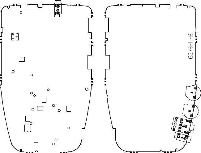
Adjustment And Test Point Locations
CP238
T200
VR730
CP750
CP711
CP101
CP725
CP324
CP705
VR710 |
|
CP344 |
CP108 |
|
|
VR303 |
VR100 |
|
CP109 |
VR300 |
|
CP308 |
|
T300 |
CP105 |
VR301 |
CP106 |
|
CP107 |
Top View Bottom View
— 3 —
Adjustment procedures (EV-660C/I/N)
1. VCC2 adjustment, VCC7, VCC6, VCC5, VEE1 voltage check
∙ Condition
(1) Signal No signal
(2) Other conditions
Power supply: Vcc1-1 = 5.00 ± 0.05 [V]
∙ Adjustment
Apply 5.00 ± 0.05 [V] on Vcc1-1.
Adjust VR100 so that Vcc2 (CP108) voltage becomes 4.80 ± 0.02 [V].
∙ Checking
VCC7 (CP105) = 27.1 ~ 33.4 [V] VCC6 (CP106) = 18.0 ~ 20.0 [V] VCC5 (CP107) = 11.0 ~ 13.0 [V] VEE1 (CP109) = –12.0 ~ –10.0 [V]
∙ Block diagram |
VCC7 |
|
|
|
|
|
|
||
|
L-PCB |
|
|
|
|
VCC6 |
|
|
|
|
VCC1-1 |
|
|
|
Stabilizer |
VCC5 |
|
Digital |
|
VCC2 |
V |
|||
|
Voltmeter |
|||
|
|
|
||
|
VEE1 |
|
|
2.LLD coil adjustment
∙Conditions
(1)Signals
Broadcasting system: B/G Color system: PAL color bar
(2)Signal level
Input electric field: 46 ± 3 dBμ (IF AGC full gain), P/S = 10 dB
(3)Other conditions
CCIR IF (Input electric field: terminated with 75 Ω resistance)
As to VIDEO signal, use signal source equivalent to TG7. Power supply: Vcc1-1 = 5.00 ± 0.05 [V]
∙Adjustment
Monitor video detection signal (CP238) via a low-pass filter of 100 kHz cutoff frequency and adjust LLD coil T200 so that its DC level is minimum (waveform’s amplitude is maximum).
∙Confirmation
There should be no waveform distortion (erroneous synchronization, etc.), under sensitivity (video detector output level is abnormally small, etc.).
∙Block diagram
|
|
L-PCB |
|
|
|
|
Signal |
IF signal |
|
|
|
|
|
generator |
|
|
|
|
|
Adjust to minimize the DC level. |
|
|
|
|
|
||
|
|
|
|
|
|
|
|
|
Detector OUT |
|
|
|
|
|
|
|
|
|
|
|
|
VCC1-1 |
|
|
|
|
|
|
|
|
|
|
||
Stabilizer |
|
|
|
DC IN |
|
|
|
|
|
|
|||
|
|
|
|
|
||
|
|
Low-Pass Filter |
|
Oscilloscope |
|
|
|
||||||
|
|
|
|
|
|
|
— 4 —
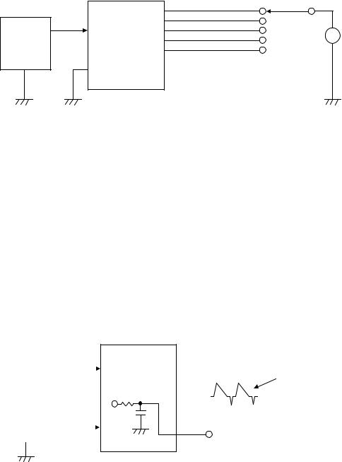
3.Free running frequency adjustment
∙Conditions
(1)Signal
No signal (PAL standard signal should be applied only at synchronous check)
(2)Signal level
Input electric field only at synchronous check: 70 ± 3 dBμ (terminated with 75Ω resistance), P/S = 10 dB
(3)Other conditions
CCIR IF input only at synchronous check (input electric field with 75 Ω termination).
Connect SYF terminal (CP725) and GND. Power supply: Vcc1-1 = 5.00 ± 0.05 [V] Room temperature: 20 ± 10 [°C]
∙Adjustment
Monitoring HDB (CP705) with a frequency counter, adjust VR710 so that the frequency is 15.625 ± 0.1 [kHz].
∙Caution
(1)Disconnect the wire between SYF terminal. Applying IF signal make sure that synchronization is normal on the display.
∙Block diagram
Signal |
IF signal |
|
|
generator |
|
|
|
VCC1-1
Stabilizer
SYF |
|
GND |
L-PCB |
HDB |
Frequency |
|
|
Counter |
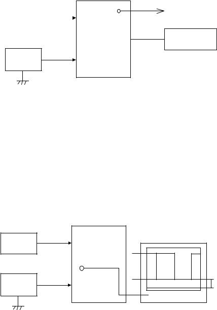
4.VCOM AC and VCOM DC coarse adjustment
•Conditions
(1)Signals
Broadcasting system: B/G Color system: PAL color bar
(2)Signal level
Input electric field: 70 ± 3dBμ (terminated with 75Ω resistance), P/S = 10 dB
(3)Others
CCIR IF input (input electric field should be terminated with 75Ω resistance)
Use VIDEO signal equivalent to TG7.
Power supply should be Vcc1-1 = 5.00 ± 0.05V.
•Adjustment
(1)Confirm that the amplitude of VCOM output (CP750) is 6.0 ± 0.5 [V].
(2)Adjust VR730 so that Low level voltage of VCOM output (CP750) is 2.4 ± 0.2 [V].
∙ Block diagram
L-PCB
IF signal
Signal generator
CP750
VCC1-1
Stabilizer
6.0 V
2.4 V
 GND
GND
 Oscilloscope
— 5 —

5.Contrast, Bright adjustment
•Conditions
(1)Signals
Broadcasting system: B/G Color system: PAL color bar
(2)Signal level
Input electric field: 70 ± 3 dBμ (terminated with 75Ω resistance), P/S = 10 dB
(3)Others
CCIR IF input (input electric field should be terminated with 75Ω resistance)
As to VIDEO signal, use signal source equivalent to TG7. Supplying power should be VCC1-1 = 5.00 ± 0.05 V
∙ Adjustment
(1) Apply VCC2-3 (CP344) voltage on KILLER terminal (CP308) via 22 kΩ resistance.
(2) Triggering FRP signal (CP711), observe VB waveform (CP324) and adjust BRIGHT VR so that pedes- tal-pedestal voltage becomes 5.0 ± 0.1[V].
(3) Adjust VR303 so that VB (CP324) waveform's pedestal - white peak voltage is 3.5 ± 0.1[V].
∙ Caution
(1) Make sure that waveforms are not distorted.
(2) After the adjustment, disconnect VCC2-3 voltage from the killer terminal.
(Reference: Use white 75% for PAL color bar.)
(3) Do not move BRIGHT VR until TINT and COLOR adjustments are completed.
∙ Block diagram |
|
|
|
|
|
VCC2-3 |
||||||||||||||||||||||||||||||
|
|
|
|
|
|
|
||||||||||||||||||||||||||||||
|
|
IF signal |
|
L-PCB |
|
22 KΩ |
||||||||||||||||||||||||||||||
|
Signal |
|||||||||||||||||||||||||||||||||||
|
|
|
|
|
|
|
|
|
|
|
|
|
|
|
|
|
|
|
|
|
|
|
|
|
|
|
|
|
|
|
|
|
|
|
||
|
|
|
|
|
|
|
|
|
|
|
|
|
|
|
|
|
|
|
|
|
|
|
|
|
|
|
|
|
|
|
|
|
|
|
|
|
|
generator |
|
|
CP308 |
|
|
|
|
|
|
|
|
|
|
|
|
|
|
|
|
|
|
|
|
|
|
|
|
|
|
|
|
|
|
|
|
|
|
|
|
|
|
|
|
|
|
|
|
|
|
|
|
|
|
|
|
|
|
|
|
|
|
|
|
|
|
|
|
|
|
|
||
|
|
|
|
B output |
|
|
|
|
|
|
|
|
|
|
|
|
|
|
|
|
|
|
|
|
|
|
|
|
|
|
|
|
|
|
|
V |
|
|
|
|
|
|
|
|
|
|
|
|
|
|
|
|
|
|
|
|
|
|
|
|
|
|
|
|
|
|
|
|
|
|
|||
|
|
|
|
|
|
|
|
|
|
|
|
|
|
|
|
|
|
|
|
|
|
|
|
|
|
|
|
|
|
|
|
|||||
|
|
|
|
|
0.1 V |
|
|
|
|
|
|
|
|
|
|
|
|
|
|
|
|
|
|
|
|
|
|
|
|
|
|
|
|
|
|
– 0.1 |
|
|
|
|
|
|
|
|
|
|
|
|
|
|
|
|
|
|
|
|
|
|
|
|
|
|
|
|
|
|
|
|
|
||||
|
Stabilizer |
VCC1-1 |
|
|
3.5 – |
|
|
|
|
|
|
|
|
|
|
|
|
|
|
|
|
|
|
|
|
|
|
|
|
|
|
|
|
|
|
5.0 |
|
|
|
|
|
|
|
|
|
|
|
|
|
|
|
|
|
|
|
|
|
|
|
|
|
|
|
|
|
|
|
|
|
|
|
|
|
|
|
|
|
|
|
|
|
|
|
|
|
|
|
|
|
|
|
|
|
|
|
|
|
|
|
|
|
|
|
|
|
|
|
|
|
|
|
|
|
|
|
|
|
|
|
|
|
Oscilloscope |
|
|
|||||||||||||||||||||||
|
|
|
|
|
|
|
||||||||||||||||||||||||||||||
|
|
|
|
|
|
|
|
|
|
|
|
|
|
|
|
|
|
|
|
|
|
|
|
|
|
|
|
|
|
|
|
|
|
|
|
|
— 6 —
 Loading...