

Page 1
R
CTK-500
(with price)
ELECTRONIC KEYBOARD
CTK-500
Page 2

CONTENTS
Specifications . . . . . . . . . . . . . . . . . . . . . . . . . . . . . . . . . . . . . . . . . . 1
Block Diagram . . . . . . . . . . . . . . . . . . . . . . . . . . . . . . . . . . . . . . . . . 2
Circuit Description . . . . . . . . . . . . . . . . . . . . . . . . . . . . . . . . . . . . . 3
Major Waveforms . . . . . . . . . . . . . . . . . . . . . . . . . . . . . . . . . . . . . . . 7
PCB Views and Major Check Points . . . . . . . . . . . . . . . . . . . . . . . . 8
Schematic Diagrams . . . . . . . . . . . . . . . . . . . . . . . . . . . . . . . . . . . . 9
Troubleshooting . . . . . . . . . . . . . . . . . . . . . . . . . . . . . . . . . . . . . . 11
IC and Transistor Lead Identification . . . . . . . . . . . . . . . . . . . . . 12
Exploded View . . . . . . . . . . . . . . . . . . . . . . . . . . . . . . . . . . . . . . . . 14
Parts List . . . . . . . . . . . . . . . . . . . . . . . . . . . . . . . . . . . . . . . . . . . . . 15
- 2 -
Page 3

SPECIFICATIONS
General
Number of Keys: 61
Polyphonic: 16-note
Preset Tones: 120
Auto-Rhythms: 40
Auto-Accompaniment: CASIO Chord/Fingered
Jukebox Tunes: 40
Chord Memory: Real-Time Recording
Memory Capacity: 128 chords (maximum)
Built-In Speakers: 12 cm dia. 1.1W Input Rating: 2 pcs.
Terminals: Output Jack [Output Impedance: 50 Ω, Output Voltage: 1.4 V (rms)MAX],
AC Adapter Jack (DC 9 V)
Auto Power Off: Approximately 6 minutes after the last operation
Power Source: 2-way AC or DC source
AC: AC adapter
DC: 6 D size dry batteries
Power Consumption: 6.7 W
Dimentions: 110 x 939 x 337 mm (HWD)
(4-5/16 x 36-15/16 x 13-1/4 inches) (HWD)
Weight: 4.5 kg (9.9 lbs) excluding batteries
Electrical
Current Drain with 9V DC:
No Sound Output 125 mA ± 30%
Maximum Volume 530 mA ± 30%
with keys C4 to D#5 pressed in Clarinet tone,
Volume; Maximum, Rhythm; Samba,
Tempo; Maximum
Output Level (Vrms with 8 Ω load each channel): 107 mV ± 30%
with key C4 pressed in Clarinet tone,
Volume; Maximum
Sound Pressure Level: 107 dB ± 10 dB
at 10 cm away from the speaker with key G6
in Brass-1 tone
Minimum Operating Voltage: 6.0 V
— 1 —
Page 4
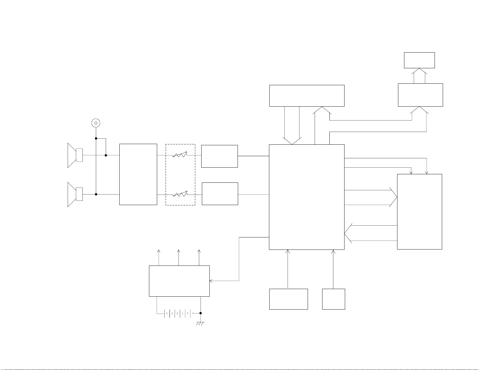
BLOCK DIAGRAM
LEDs
— 2 —
Speakers
Output
Power Amp.
LA4127
IC2
Main Volume
Control
VCCAVDDVDD
Filter (R)
T5
Filter (L)
T6
KI1 ~ KI7
ROUT
LOUT
KO18
Keys and Switches
CPU
MSM6626-01
LSI1
KO0 ~ KO16
A0 ~ A16
D0 ~ D15
LED Driver
IC3
KO0 ~ KO5, KO17
CE
OE
ROM
MN232000CUQ
LSI2
Power IC
CA5668
IC1
(APO)
Reset IC
S8053ANO
IC4
43.45 MHz Clock
X1
Page 5
CIRCUIT DESCRIPTION
Key and Switch Matrix
KI0 KI1 KI2 KI3 KI4 KI5 KI6 KI7
KO0 C2 C#2 D2 D#2 E2 F2
KO1 F#2 G2 G#2 A2 A#2 B2
KO2 C3 C#3 D3 D#3 E3 F3
KO3 F#3 G3 G#3 A3 A#3 B3
KO4 C4 C#4 D4 D#4 E4 F4
KO5 F#4 G4 G#4 A4 A#4 B4
KO6 C5 C#5 D5 D#5 E5 F5
KO7 F#5 G5 G#5 A5 A#5 B5
KO8 C6 C#6 D6 D#6 E6 F6
KO9 F#6 G6 G#6 A6 A#6 B6
KO10 C7
KO11
KO12
KO13 Reverb Off Reverb 1 Reverb 2
KO14
KO15 Bank A Bank B Bank C Bank D Bank E Bank F Bank G Bank H
KO16 Number 1 Number 2 Number 3 Number 4 Number 5
Power
Off
Accomp.
Volume 1
(Min)
Synchro
/ Fill-In
Normal Fingered
Accomp.
Volume 2
Start/Stop
Accomp.
Volume 3
Intro/
Ending
CASIO
Chord
Accomp.
Volume 4
Chord
Memory
Record
Tempo
Up
Accomp.
Volume 5
(Max)
Chord
Memory
Play
Tempo
Down
Ad-Lib
Musician
Solo
Sound
Jukebox
Start/Stop
Duo
Sound
Beat
(Jukebox)
Ensenble
Sound
— 3 —
Page 6
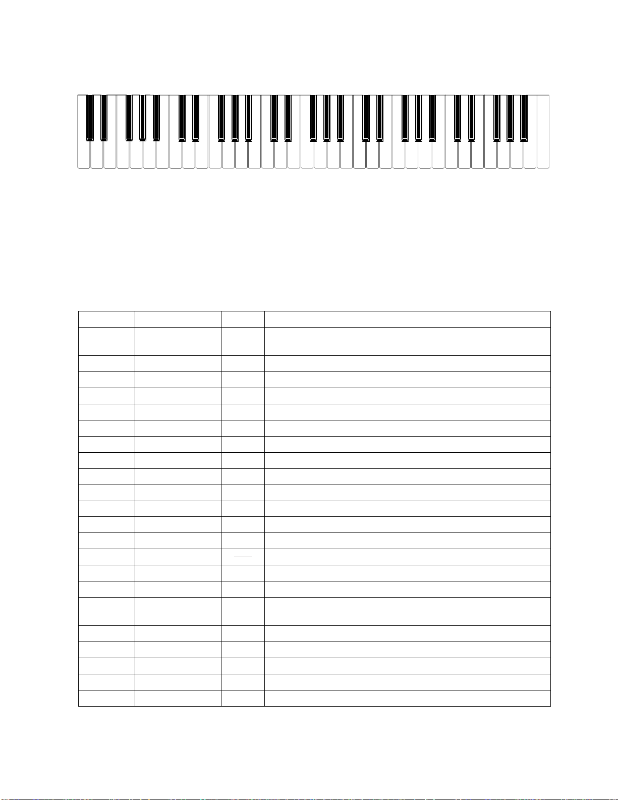
Nomenclature of Keys
C#2
C2 D2E2F2G2A2 B2 C3 D3
F#2D#2
C#3A#2G#2
F#3 G#3
D#3
E3
F3 G3 A3 B3 C4 D4 E4 F4 G4 A4 B4 C5 D5 E5 F5 G5 A5 B5
A#3 C#4 D#4
F#4 G#4
A#4
C#5
D#5
F#5 G#5
A#5
C#6
C6
G#6F#6D#6
A#6
B6A6G6F6E6D6
CPU (LSI1: MSM6626-01)
The CPU reads sound data from the ROM in accordance with the pressed key and the selected tone; the
CPU can read rhythm data simultaneously when a rhythm pattern is selected. Then it provides the left
and the right channels' waveforms separately, by converting the data into the waveforms with two built-in
DACs. The CPU also controls keys, switches, and LEDs.
The following table shows the pin functions of LSI1.
Pin No. Terminal In/Out Function
1 ~ 10
74 ~ 80
KO0 ~ KO16 Out
Using time sharing, the terminals provide key and switch
scan signals, and LED drive signals.
11 KO17 Out Clock output for the LED driver
12 KO18 (APO) Out APO (Auto Power Off) signal output.
13 KO20 Out Not used.
14 ~ 21 KI0 ~ KI7 In Input terminals from the keys and switches
22 -MI In Power ON trigger pulse input.
23 -RESET In CPU reset signal input.
24 REFH In Low level reference voltage input for the built-in DAC
25 AVDD In +5 V source for the built-in DAC
26 ROUT Out Right channel sound signal output
27 LOUT Out Left channel sound signal output
28 AGND In Ground (0 V) source for the built-in DAC
29 REFL In High level reference voltage for the built-in DAC
30, 31 TEST1, TEST2 Not used. Connected to ground.
32 GND In Ground (0 V) source
33, 34 COSI, COSO In/Out 43.45 MHz clock input/output
35 VDD In
+5 V DC source. Regardless of the power switch position,
the terminal always receives +5 V DC.
36 -CE Out Chip enable signal output. Low effective.
37 -OE Out Read enable signal output. Low effective.
38 ~ 40 ADR17 ~ ADR19 Out Not used.
41 ~ 57 ADR0 ~ ADR16 Out Address bus for the ROM
58 ~ 73 DIN0 ~ DIN15 In Data bus for the ROM
C7
— 4 —
Page 7
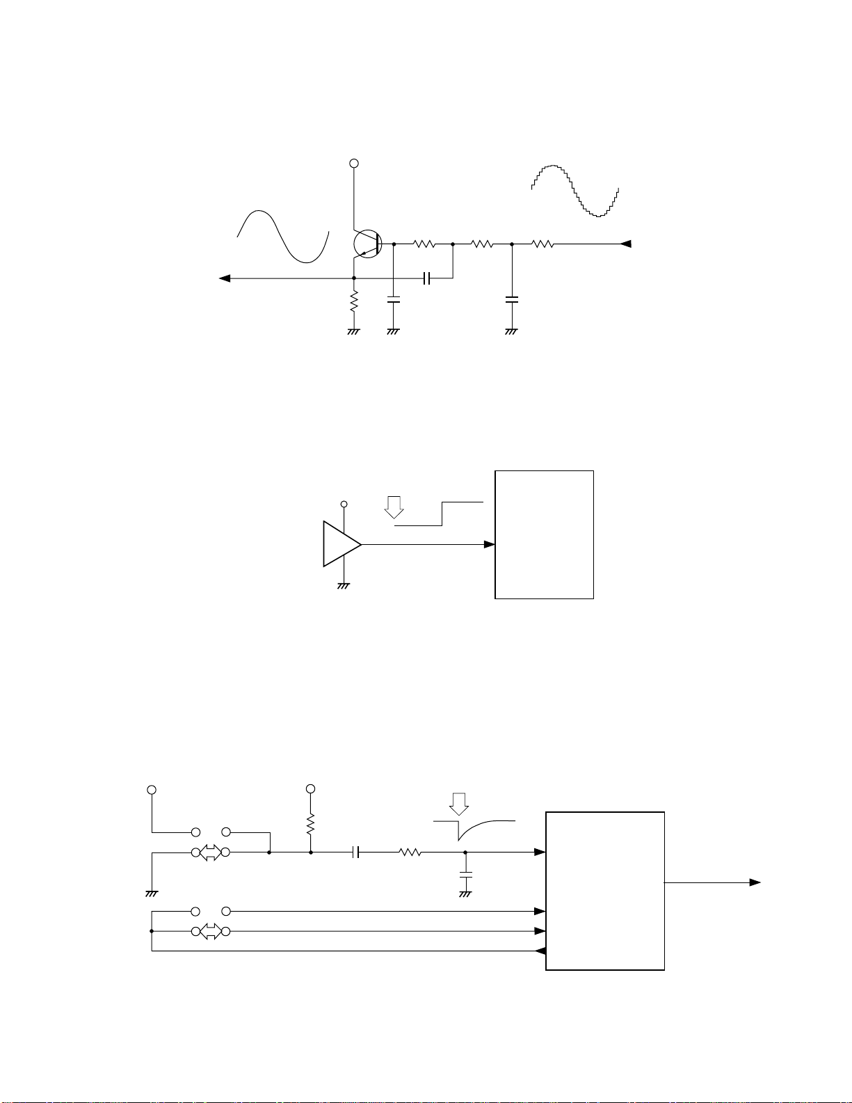
FIlter Block
Since the sound signall from the CPU is a stepped waveform, the filter block is added to smooth the
waveform.
VDD
2SC3112B
10K
10K 6.2K
From the CPU
To main volume
1K
AG
C331J
AG
C562(H)
C222(H)
AG
Initial Reset Circuit
When batteries are set or an AC adapter is connected, the reset IC provides a low pulse to the CPU.
The CPU then initializes its internal circuit.
VDD
Battery set
CPU
Reset IC
S8053ANO
IC4
RESET
MSM6626-01
LSI1
Power On/Off Circuit
When the power switch is turned on, a low level differential pulse is provided to terminal MI of the CPU.
Upon receipt of the pulse, the CPU starts the power ON sequence and raises the APO signal to +5 V.
When the switch is off, on receiving the KO11 signal at terminal KI0, the CPU drops the APO signal to
ground level to shut down power.
OFF
ON
OFF
ON
VDD
Power Switch
VDD
KI0
KI1
KO11
— 5 —
ON
MI
CPU
MSM6626-01
LSI1
KO18
APO signal
OFF: 0V
ON: +5 V
Page 8

Power IC (IC1: CA5668)
The power IC generates three voltages AVDD (+5 V) for the CPU and the reset IC, AVDD (+5 V) for the
analog circuit, and VCC (+9 V) for the power amplifier. VDD (+5 V) is always generated, but AVDD (+5 V)
and VCC (+ 9V) are controlled by the APO signal.
CA5668
IC1
VIN
VDIN
+9V
VDD
AVDD
APO VDD AVDD VCC
0 V +5 V 0 V 0 V
VCC
GND
+5 V +5 V +5 V +9 V
APO
LED Driving
LED Driver
TC74CH174AP
IC3
Chord Memory Play
Solo Sound
Duo Sound
Ensenble Sound
Beat (Jukebox)
Ad-Lib Musician
L0
L1
L2
L3
L4
L5
Q3
Q5
Q2
Q6
Q1
Q4
CLR
VDD
D3
D5
D2
D6
D1
D4
CLK
KO0
KO1
KO2
KO3
KO4
KO5
KO17
CPU
MSM6626-01
LSI1
— 6 —
Page 9

MAJOR WAVEFORMS
— 7 —
Page 10

1
2
3
5
6
7
89
10
11 12
13
4
Volume PCB M5505-MA2M
Main PCB M5505-MA1M
PCB VIEWS AND MAJOR CHECK POINTS
— 8 —
Page 11

M5505-MA1M,MA2M PCB
SCHEMATIC DIAGRAMS
8
5
2
9
13
4
1
12
10
11
7
6
3
— 9 —
Page 12

Keyboard PCBs M619K-KY1M,KY2M
PCB-M619K-KY1M
PCB-M619K-KY2M
— 10 —
Page 13

TROUBLESHOOTING
Nature of Trouble Faulty Block Checkpoint
No power Power Jack (J1) Jack contact.
Power IC (IC1: CA5668) Pin 8 should have +5 V.
Pin 6 should provide + 5V when pin 10
receives + 5 V.
Reset IC (IC4: S8053ANO)
Power Switch
Main Clock Generator (X1) Check oscillation at pin 34 of CPU.
Pin 1 should provide a low level pulse when
an AC adapter is connected.
Pin 22 of CPU should receive a trigger
pulse when turning on the switch.
CPU (LSI1: MSM6626-01)
No sound at all Power Amp. (IC2: LA4127) Check output waveforms of pins 9 and 12.
CPU (LSI1: MSM6626-01) Check output waveforms of pins 25 and 26.
ROM (LSI2: MN232000CUQ)
Distorted sound ROM (LSI2: MN232000CUQ) Check address/data bus.
CPU (LSI1: MSM6626-01) Check output waveforms of pins 25 and 26.
Power Amp. (IC2: LA4127) Check output waveforms of pins 9 and 12.
Power IC (IC1: CA5668)
All or certain keys do
not function
A certain key does not
function
CPU (LSI1: MSM6626-01)
Key Matrix Open circuit on KO or KI line.
Key Matrix Dust on the contact.
Pin 12 should provide +5 V when turning on
the power switch.
Check CE signal of pin 10, and OE signal
of pin 12.
Check voltages of pins 2 (+9 V) and 6
(+5 V).
Check KO signals of pins 1 to 4, and 74 to
80.
— 11 —
Page 14
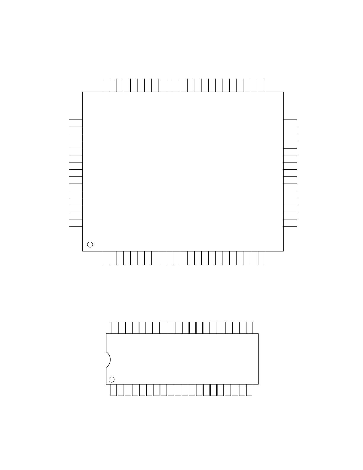
IC AND TRANSISTOR LEAD IDENTIFICATION
LSI1: MSM6626-01
65
66
67
68
69
70
71
72
73
74
75
76
77
78
79
80
6463626160595857565554535251504948474645444342
DIN9
DIN10
DIN11
DIN12
DIN13
DIN14
DIN15
ADR0
ADR1
ADR2
ADR3
ADR4
ADR5
ADR6
ADR7
ADR8
ADR9
ADR10
DIN8
DIN7
DIN6
DIN5
DIN4
DIN3
DIN2
DIN1
DIN0
KO0
KO1
KO2
KO3
KO4
KO5
KO6
KO7
KO8
KO9
KO10
KO11
KO12
KO13
KO14
KO15
KO16
KO17
KO18
KO20
KI0
KI1
KI2
KI3
KI4
123456789
101112131415161718192021222324
ADR11
ADR12
KI5
KI6
ADR13
ADR14
ADR15
ADR17
ADR18
ADR19
KI7
-MI
-RESET
41
ADR16
-OE
-CE
VDD
COSO
COSI
GND
TEST1
TEST2
REFL
AGND
LOUT
ROUT
AVDD
REFH
40
39
38
37
36
35
34
33
32
31
30
29
28
27
26
25
LSI2: MN232000CUQ
40393837363534333231302928272625242322
A8
A9
A10
A11
A12
A13
A14
A15
A16
NCA7A6A5A4A3A2A1A0
123456789
— 12 —
D15D7D14D6D13D5D12
VSS
BHE
-CE
VSS
-OED0D8D1D9D2D10D3D11
1011121314151617181920
D4
21
VCC
Page 15

IC1: CA5668
IC2: LA4127
201918171615141312
DC
VINVCVDIN
GND
VADJ
VAOU
VAGD
VDD
123456789
VDGD
APO
10
PriIN1+
PriGND
PriIN2+
1
2
PriIN2-
3
PoIN1+
PriOUT1
PriGND1
PriOUT2
PriGHD
PoIN2+
4
5
6
PriIN1-
IC3: TC74HC174AP IC4: S8053ANO
16151413121110
9
PoIN1-
BootsSt.
PoIN2-
BoostSt.
7
8
11
VCC
PoOUT1
PoOUT2
PoGND
9
10
D6
D5Q5D4
VCC
Q6
Q4
CLRQ1D1D2Q2D3Q3
1
2
3
4
5
6
7
CLK
GND
8
T5, T6: 2SC3112B
E C B
1 2 3
— 13 —
Page 16

EXPLODED VIEW
— 14 —
Page 17

PARTS LIST
CTK-500
Notes: 1. Prices and specifications are subject to change with-
out prior notice.
2. As for spare parts order and supply, refer to the
"GUIDEBOOK for Spare parts Supply", published
separately.
3. The numbers in item column correspond to the same
numbers in drawing.
Page 18

FOB Japan
N Item Code No. Parts Name Specification Q M N.R.Yen R *
Unit Price
PCB Ass'y M5505-MA1M
2011 2912 LSI MN232000CUQ 1 1 690 A G
2011 4109 LSI MSM6626-01GS-K-108 1 1 1,010 A K
2105 1071 IC TC74HC174AP 1 1 70 A B
2105 2219 IC S-8053ANO 1 1 60 A B
2114 0070 IC LA4127 1 1 180 A C
2114 1239 IC CA5668 1 1 160 A B
2252 0721 Transistor 2SC3113B-TPE4-T 2 10 16 A A
2360 1939 Zener diode MTZJ5.1C-T77-T 1 20 12 A A
N 2370 0987 LED LN28RPX-(TT14) 7 20 17 C A
2390 0371 Diode DSK10B-BT-T 2 20 11 B A
2390 1344 Diode 1SS133T-77-T 14 20 3 C A
2590 1190 Ceramic oscillator EFO-GC4345C3 1 1 130 B B
2609 0175 Carbon film resistor ERD-S2TJ-3R3T-T 2 20 3 C A
2609 0245 Carbon film resistor ERD-S2TJ-622T-T 2 20 2 C A
2609 0287 Carbon film resistor ERD-S2TJ-270T-T 2 20 2 C A
2616 0324 Carbon film resistor ERD-S2TJ-100T-T 1 20 3 C A
2616 0332 Carbon film resistor ERD-S2TJ-101T-T 28 20 3 C A
2616 0340 Carbon film resistor ERD-S2TJ-331T-T 6 20 2 C A
2616 0375 Carbon film resistor ERD-S2TJ-102T-T 4 20 3 C A
2616 0413 Carbon film resistor ERD-S2TJ-472T-T 2 20 3 C A
2616 0430 Carbon film resistor ERD-S2TJ-103T-T 8 20 3 C A
2616 0464 Carbon film resistor ERD-S2TJ-473T-T 1 20 3 C A
2616 0570 Carbon film resistor ERD-S2TJ-123T-T 1 20 2 C A
2616 0588 Carbon film resistor ERD-S2TJ-471T-T 1 20 3 C A
2616 0634 Carbon film resistor ERD-S2TJ104T-T 2 20 3 C A
2616 0677 Carbon film resistor ERD-S2TJ-220T-T 5 20 3 C A
2801 7196 Electrolytic capacitor 10RE2-33-T2-T 2 20 13 C A
2801 7469 Electrolytic capacitor ECE-A1CU471ZB-T 2 10 29 C A
2801 8176 Electrolytic capacitor ECE-A1CU220B-T 1 10 12 C A
2801 8197 Electrolytic capacitor ECE-A1AU101B-T 2 10 13 C A
2801 8204 Electrolytic capacitor ECE-A1CU221B-T 1 10 22 C A
2801 8211 Electrolytic capacitor ECE-A0JU101B-T 4 10 13 C A
2801 8449 Electrolytic capacitor ECE-A1CU101B-T 1 10 17 C A
2801 9121 Electrolytic capacitor ECE-A0JU471B-T 3 10 21 C A
2801 9128 Electrolytic capacitor ECE-A0JU221B-T 4 10 17 C A
2801 9821 Electrolytic capacitor ECE-A1AU220B-T 2 10 10 C A
2805 0526 Electrolytic capacitor 10RE2-1000 2 10 30 C A
2807 1023 Electrolytic capacitor 50RE2-1-T2-T 1 10 15 C A
2813 0245 Semiconductive capacitor RT-C50TKYR103K-T 3 20 7 C A
2813 1302 Semiconductive capacitor RT-B90TKYR104K-T 8 20 10 C A
2813 1393 Semiconductive capacitor RT-C40TKYR222K-T 2 20 10 C A
2813 1400 Semiconductive capacitor RT-C50TKYR562K-T 2 20 5 C A
2818 0365 Ceramic capacitor RT-HE50TKYB102K-T 2 20 3 C A
2818 0446 Ceramic capacitor RT-HE40TKYB101K-T 7 20 4 C A
2818 0494 Ceramic capacitor RT-HE80TKSL331J-T 2 20 9 C A
2818 1221 Ceramic capacitor RT-HE40TKCH050D-T 1 20 5 C A
2819 5460 Module capacitor CNB5X101K 1 10 35 C A
2830 6229 Mylar capacitor AMZV-104K50-T 2 10 13 C A
2845 0014 Module capacitor CNB8X561M 1 5 60 C B
2845 0182 Module capacitor CNB6X101K 1 5 43 C A
2845 0280 Ferrite beads EXC-ELDR35C 2 20 13 C A
2845 2261 Three-polarity capacitor EXC-ECT223ZVC 3 20 13 C A
3501 7049 DC jack HEC2305-01-330 1 5 29 A A
3612 0711 Miniature jack YKB21-5101 1 5 90 B B
Notes: N – New parts
M – Minimum order/supply quantity
R – Rank
— 15 —
Page 19

FOB Japan
N Item Code No. Parts Name Specification Q M N.R.Yen R *
Unit Price
3719 2317 Ribbon cable M237S DF0H02110-35358035 1 10 16 C A
3719 3584 Ribbon cable M505C (4-pin) DF5H04135-MM 1 10 19 C A
3719 3591 Ribbon cable M505D DF5H02290-MM 1 10 20 C A
3719 3598 Ribbon cable M505L DF5H02160-35358035 1 10 20 C A
N 3841 0959 Inductor ELE-R100KR-T 5 10 25 C A
4317 3042 Blank PCB M5505-MA1M M111131B-1 1 1 800 C I
2765 1211 Slide volume EWA-MJCC20B23 1 1 110 B B
JB 3719 3577 Ribbon cable M505B (5-pin) DF5H05100-MM 1 10 18 C A
4317 3052 Blank PCB M5505-MA2M M111131B-2 1 10 13 C A
3665 0238 Pin assembly IMSA-1068-17Z174 1 5 67 C B
4317 3030 Blank PCB M5505-MA3 M211408-1 1 10 11 C A
N 6922 5200 PCB ass'y M5505-MA1M,2M,3 M111130*2 1 1 5,100 B AA
PCB Ass'y Keyboard
2305 5023 Diode 1S1588-TP3-T 61 20 8 C A
JX 3725 2527 PC joiner MASK61 JSF50-11-160 1 10 42 C A
JA 0009 2467 PC joiner M505A JSF50-17-240M 1 5 90 C B
4317 2611 Blank PCB M619K-KY1M M111074A-1 1 1 130 C B
4317 2620 Blank PCB M619K-KY2M M111075-1 1 1 110 C B
Keyboard Ass'y
1 6917 4474 White key set CEGB M110589D-1 5 1 120 A B
2 6917 4484 White key set DFAS M110590D-1 1 1 110 A B
3 6917 4494 White key set DFA M110591D-1 4 1 170 A B
4 6917 4506 Black key 10P M110594F-1 2 1 130 A B
5 6918 5996 Black key 5P M110594F-3 1 5 81 A B
6 6917 4453 TAC 31 M110603C-1 1 1 190 B C
7 6919 0410 TAC30 M110930-1 1 1 190 B C
6919 4330 Felt ASK-L M411714-1 1 20 14 C A
6919 4340 Felt ASK-R M411715-1 1 20 14 C A
8 6919 5630 KB chassis 61B-GD M111053-1 1 1 1,340 C O
Case
9 6919 5330 Slide knob 271 M311521-1 3 20 13 B A
10 6919 5340 Slide volume knob 271 M311530-1 1 20 13 B A
N 11 6922 5711 Upper case sub ass'y M211767A*1 1 1 1,230 C N
12 6909 5890 SL contact12D CSB-12D 3 10 35 B A
13 6921 1250 Button M505A M311534-3 5 10 22 B A
14 6920 7160 Button M505A M311534-2 1 10 22 B A
15 6920 7120 Button M505B M211342-1 1 1 190 B C
16 6920 7151 Contact rubber M505A M311675A-1 1 1 110 B B
17 6920 7130 Button M505C M211343-1 1 1 150 B B
18 6920 9960 Button M505D M211344-2 1 5 96 B B
19 3831 0357 Speaker 1221AF 2 1 1,000 B K
N 20 6922 5732 Lower case sub ass'y M211236L*17 1 1 1,210 C M
20-1 6902 6140 Battery spring 90 (-) M41226-1 1 10 27 C A
20-2 6903 2150 Battery sparing B (+) M41330-1 1 10 18 C A
20-3 6919 3190 Key damper 61 M411615-1 1 5 55 C A
N 6922 5080 Rating plate M311202-43 1 10 13 C A
N 21 6906 6054 Battery cover sub ass'y M311164D*6 1 1 210 B C
Screws
22 0009 2682 Screw 2.6 x 8 22 50 2 C C
23 0009 2680 Screw 4 x 8 10 50 2 C C
24 0009 2637 Screw 3 x 18 11 50 2 C C
N 25 0009 2698 Screw 3 x 14 15 50 2 C C
26 6919 0420 Screw 3 x 8 M411481-1 12 50 2 C C
N 27 0002 1116 Screw 4 x 8 11 50 2 C C
28 5111 2679 Screw 3 x 8 6 50 2 C C
Notes: N – New parts
M – Minimum order/supply quantity
R – Rank
— 16 —
Page 20

FOB Japan
N Item Code No. Parts Name Specification Q M N.R.Yen R *
Unit Price
Accessory
6916 7880 Music stand M310827-1 1 120 C B
Notes: N – New parts
M – Minimum order/supply quantity
R – Rank
— 17 —
Page 21

MA0300941A
 Loading...