

Page 1

MU195020A
Operation Manual
●
For safety and warning information, please read this
●
Additional safety and warning information is provided
before using
●
21G/32G bit/s SI PPG
MU195040A
21G/32G bit/s SI ED
MU195050A
Noise Generator
manual before attempting to use the equipment.
within the MP1900A Signal Quality Analyzer-R
Operation Manual. Please also refer to it
the equipment.
Keep this manual with the equipment.
11th Edition
ANRITSU CORPORATION
Document No.: M-W3915AE-11 .0
Page 2
Safety Symbols
DANGER
WARNING
CAUTION
To prevent the risk of personal injury or loss related to equipment malfunction, Anritsu Corporation uses the following
safety symbols to indicate safety-related information. Ensure that you clearly understand the meanings of the symbols
BEFORE using the equipment. Some or all of the following symbols may be used on all Anritsu equipment. In addition,
there may be other labels attached to products that are not shown in the diagrams in this manual.
Symbols used in manual
This indicates a very dangerous procedure that could result in serious injury or
death if not performed properly.
This indicates a hazardous procedure that could result in serious injury or death if
not performed properly.
This indicates a hazardous procedure or danger that could result in light-to-severe
injury, or loss related to equipment malfunction, if proper precautions are not taken.
Safety Symbols Used on Equipment and in Manual
The following safety symbols are used inside or on the equipment near operation locations to provide information
about safety items and operation precautions. Ensure that you clearly understand the meanings of the symbols and
take the necessary precautions BEFORE using the equipment.
This indicates an obligatory safety precaution. The obligatory operation is
This indicates a warning or caution. The contents are indicated symbolically in or
This indicates a note. The contents are described in the box.
These indicate that the marked part should be recycled.
This indicates a prohibited operation. The prohibited operation is indicated
symbolically in or near the barred circle.
indicated symbolically in or near the circle.
near the triangle.
MU195020A 21G/32G bit/s SI PPG
MU195040A 21G/32G bit/s SI ED
MU195050A Noise Generator Operation Manual
19 June 2017 (First Edition)
5 March 2021 (11th Edition)
Copyright © 2017-2021, ANRITSU CORPORATION.
All rights reserved. No part of this manual may be reproduced without the prior written permission of the
publisher.
The operational instructions of this manual may be changed without prior notice.
Printed in Japan
ii
Page 3

Equipment Certificate
Anritsu Corporation certifies that this equipment was tested before shipment
using calibrated measuring instruments with direct traceability to public
testing organizations recognized by national research laboratories, including
the National Institute of Advanced Industrial Science and Technology, and
the National Institute of Information and Communications Technology, and
was found to meet the published specifications.
Anritsu Warranty
Anritsu Corporation will repair this equipment free-of-charge if a malfunction
occurs within one year after shipment due to a manufacturing fault, and
software bug fixes will be performed in accordance with the separate Software
End-User License Agreement, provide, however, that Anritsu Corporation will
deem this warranty void when:
The fault is outside the scope of the warranty conditions separately
●
described in the operation manual.
The fault is due to mishandling, misuse, or unauthorized modification or
●
repair of the equipment by the customer.
The fault is due to severe usage clearly exceeding normal usage.
●
The fault is due to improper or insufficient maintenance by the customer.
●
The fault is due to natural disaster, including fire, wind or flood,
●
earthquake, lightning strike, or volcanic ash, etc.
The fault is due to damage caused by acts of destruction, including civil
●
disturbance, riot, or war, etc.
The fault is due to explosion, accident, or breakdown of any other
●
machinery, facility, or plant, etc.
The fault is due to use of non-specified peripheral or applied equipment
●
or parts, or consumables, etc.
The fault is due to use of a non-specified power supply or in a non-
●
specified installation location.
The fault is due to use in unusual environments
●
The fault is due to activities or ingress of living organisms, such as
●
insects, spiders, fungus, pollen, or seeds.
In addition, this warranty is valid only for the original equipment purchaser. It
is not transferable if the equipment is resold.
Anritsu Corporation shall assume no liability for damage or financial loss of
the customer due to the use of or a failure to use this equipment, unless the
damage or loss is caused due to Anritsu Corporation’s intentional or gross
negligence.
(Note)
.
iii
Page 4

Note:
For the purpose of this Warranty, "unusual environments" means use:
In places of direct sunlight
●
In dusty places
●
Outdoors
●
In liquids, such as water, oil, or organic solvents, and medical fluids, or
●
places where these liquids may adhere
In salty air or in place chemically active gases (sulfur dioxide, hydrogen
●
sulfide, chlorine, ammonia, nitrogen dioxide, or hydrogen chloride etc.)
are present
In places where high-intensity static electric charges or electromagnetic
●
fields are present
In places where abnormal power voltages (high or low) or instantaneous
●
power failures occur
In places where condensation occurs
●
In the presence of lubricating oil mists
●
In places at an altitude of more than 2,000 m
●
In the presence of frequent vibration or mechanical shock, such as in
●
cars, ships, or airplanes
Anritsu Corporation Contact
In the event of this equipment malfunctions, please contact an Anritsu
Service and Sales office. Contact information can be found on the last page
of the printed version of this manual, and is available in a separate file on the
PDF version.
iv
Page 5

This product and its manuals may require an Export License/Approval by
the Government of the product's country of origin for re-export from your
country.
Before re-exporting the product or manuals, please contact us to confirm
whether they are export
When
controlled items, the products/manuals need to
be broken/shredded so as not to be unlawfully used for military purpose.
you dispose of export-
Notes On Export Management
-controlled items or not.
v
Page 6

Crossed-out Wheeled Bin Symbol
Equipment marked with the Crossed-out Wheeled Bin Symbol complies with
council directive 2012/19/EU (the “WEEE Directive”) in European Union.
For Products placed on the EU market after August 13, 2005, please contact
your local Anritsu representative at the end of the product's useful life to
arrange disposal in accordance with your initial contract and the local law.
vi
Page 7

Software End-User License Agreement (EULA)
Please carefully read and accept this Software End-User License Agreement (hereafter this EULA)
before using (includes executing, copying, installing, registering, etc.) this Software (includes programs,
databases, scenarios, etc., used to operate, set, etc., Anritsu electronic equipment, etc.). By using this
Software, you shall be deemed to have agreed to be bound by the terms of this EULA, and Anritsu
Corporation (hereafter Anritsu) hereby grants you the right to use this Software with the Anritsu
specified equipment (hereafter Equipment) for the purposes set out in this EULA.
Article 1. Grant of License and Limitations
1. You may not to sell, transfer, rent, lease,
lend, disclose, sublicense, or otherwise
distribute this Software to third parties,
whether or not paid therefor.
2. You may make one copy of this Software for
backup purposes only.
3. You are not permitted to reverse engineer,
disassemble, decompile, modify or create
derivative works of this Software.
4. This EULA allows you to install one copy of
this Software on one piece of Equipment.
Article 2. Disclaimers
To the extent not prohibited by law, in no
event shall Anritsu be liable for direct, or
any incidental, special, indirect or
consequential damages whatsoever,
including, without limitation, damages for
loss of profits, loss of data, business
interruption or any other commercial
damages or losses, and damages claimed by
third parties, arising out of or related to your
use or inability to use this Software, unless
the damages are caused due to Anritsu’s
intentional or gross negligence.
Article 3. Limitation of Liability
1. If a fault (bug) is discovered in this Software,
failing this Software to operate as described
in the operation manual or specifications
even though you have used this Software as
described in the manual, Anritsu shall at its
own discretion, fix the bug, or replace the
software, or suggest a workaround, free-ofcharge, provided, however, that the faults
caused by the following items and any of
your lost or damaged data whatsoever shall
be excluded from repair and the warranty.
i) If this Software is deemed to be used
for purposes not described in the
operation manual or specifications.
ii) If this Software has been used in
conjunction with other non-Anritsuapproved software.
iii) If this Software or the Equipment has
been modified, repaired, or otherwise
altered without Anritsu's prior
approval.
iv) For any other reasons out of Anritsu's
direct control and responsibility, such
as but not limited to, natural disasters,
software virus infections, or any
devices other than this Equipment, etc.
2. Expenses incurred for transport, hotel, daily
allowance, etc., for on-site repairs or
replacement by Anritsu engineers
necessitated by the above faults shall be
borne by you.
3. The warranty period for faults listed in
Section 1 of this Article shall be either 6
months from the date of purchase of this
Software or 30 days after the date of repair
or replacement, whichever is longer.
vii
Page 8

Article 4. Export Restrictions
You shall not use or otherwise export or re-
export directly or indirectly this Software
except as authorized by the laws and
regulations of Japan and the United States,
etc. In particular, this Software shall not be
exported or re-exported (a) into any Japan or
US embargoed countries or (b) to anyone
restricted by the Japanese export control
regulations, or the US Treasury
Department's list of Specially Designated
Nationals or the US Department of
Commerce Denied Persons List or Entity
List. In using this Software, you warrant
that you are not located in any such
embargoed countries or on any such lists.
You also agree that you will not use or
otherwise export or re-export this Software
for any purposes prohibited by the Japanese
and US laws and regulations, including,
without limitation, the development, design
and manufacture or production of missiles or
nuclear, chemical or biological weapons of
mass destruction, and conventional
weapons.
Article 5. Change of Terms
Anritsu may change without your approval
the terms of this EULA if the changes are for
the benefit of general customers, or are
reasonable in light of the purpose of this
EULA and circumstances of the changes. At
the time of change, Anritsu will inform you
of those changes and its effective date, as a
general rule 45
website, or in writing or by e-mail.
days, in advance on its
Article 6. Termination
1. Anritsu may terminate this EULA
immediately if you violate any conditions
described herein. This EULA shall also be
terminated immediately by Anritsu if there
is any good reason that it is deemed difficult
to continue this EULA, such as your
violation of Anritsu copyrights, patents, etc.
or any laws and ordinances, or if it turns out
that you belong to an antisocial organization
or has a socially inappropriate relationship
with members of such organization.
2. You and Anritsu may terminate this EULA
by a written notice to the other party 30
days in advance.
Article 7. Damages
If Anritsu suffers any damages or loss,
financial or otherwise, due to your violation
of the terms of this EULA, Anritsu shall
have the right to seek proportional damages
from you.
Article 8. Responsibility after Termination
Upon termination of this EULA in
accordance with Article 6, you shall cease all
uses of this Software immediately and shall
as directed by Anritsu either destroy or
return this Software and any backup copies,
full or partial, to Anritsu.
Article 9. Negotiation for Dispute
Resolution
If matters of interpretational dispute or
items not covered under this EULA arise,
they shall be resolved by negotiations in
good faith between you and Anritsu.
Article 10. Governing Law and Court of
Jurisdiction
This EULA shall be governed by and
interpreted in accordance with the laws of
Japan without regard to the principles of the
conflict of laws thereof, and any disputes
arising from or in relation to this EULA that
cannot be resolved by negotiation described
in Article 9 shall be subject to and be settled
by the exclusive agreed jurisdiction of the
Tokyo District Court of Japan.
Revision History:
February 29th, 2020
viii
Page 9

CE Conformity Marking
Anritsu affixes the CE conformity marking on the following product(s) in
accordance with the Decision 768/2008/EC to indicate that they conform to
the EMC, LVD and RoHS directive of the European Union (EU).
CE marking
1. Product Model
Plug-in Units: MU195020A 21G/32G bit/s SI PPG
MU195040A 21G/32G bit/s SI ED
MU195050A Noise Generator PG
2. Applied Directive and Standards
When the MU195020A 21G/32G bit/s SI PPG, MU195040A 21G/32G
bit/s SI ED, and MU195050A Noise Generator PG are installed in the
MP1900A, the applied directive and standards of this unit conform to
those of the MP1900A main frame.
PS: About main frame
Please contact Anritsu for the latest information on the main frame
types that MU195020A, MU195040A, and MU195050A can be used
with.
ix
Page 10

RCM Conformity Marking
Anritsu affixes the RCM mark on the following product(s) in accordance with
the regulation to indicate that they conform to the EMC framework of
Australia/New Zealand.
RCM marking
1. Product Model
Plug-in Units: MU195020A 21G/32G bit/s SI PPG
MU195040A 21G/32G bit/s SI ED
MU195050A Noise Generator PG
2. Applied Directive and Standards
When the MU195020A 21G/32G bit/s SI PPG, MU195040A 21G/32G
bit/s SI ED, and MU195050A Noise Generator PG are installed in the
MP1900A, the applied directive and standards of this unit conform to
those of the MP1900A main frame.
PS: About main frame
Please contact Anritsu for the latest information on the main frame
types that MU195020A, MU195040A, and MU195050A can be
used with.
x
Page 11
About This Manual
Configuration of Signal Quality Analyzer-R Series Operation
Describes the basic operations, panel details, and maintenance of the MP1900A, as
well as the steps from module installation to the start of u
indicates this document.
Describes the panel details, how to operate, performance test, maintenance, and
troubleshooting of the
Module Operation Manual
Operation Manual
Describes the panel details, how to operate, performance test, maintenance, and
troubleshooting of the MU181000A
Describes the panel details, how to operate, performance test and maintenance of the
MU181500B.
MU195050A Noise Generator Operation Manual
Describes the panel details, how to operate, performance test, maintenance, and
Operation Manual
Describes the panel details, performance test, maintenance, and troubleshooting of
Describes the panel details, performance test, maintenance, and troubleshooting of
the
A testing system combining an MP1900A Signal Quality Analyzer-R,
module(s), and control software is called a Signal Quality Analyzer-R
Series. The operation manuals of the Signal Quality Analyzer-R Series
consist of separate documents for the MP1900A, module(s), and control
software, as shown below.
MP1900A Signal Quality Analyzer-R Operation Manual
se.
MU195020A 21G/32G bit/s SI PPG MU195040A 21G/32G bit/s SI ED
module to be installed on the MP1900A.
MU196020A PAM4 PPG MU196040A PAM4 ED MU196040B PAM4 ED
Operation Manual
MU196020A, MU196040A, and MU196040B.
MU181000A 12.5GHz Synthesizer MU181000B 12.5GHz 4 port Synthesizer
and MU181000B.
MU181500B Jitter Modulation Source Operation Manual
MU183020A 28G/32G bit/s PPG MU183021A 28G/32G bit/s 4ch PPG
the MU183020A and MU183021A.
MU183040A 28G/32G bit/s ED MU183041A 28G/32G bit/s 4ch ED
MU183040B 28G/32G bit/s High Sensitivity ED
MU183041B 28G/32G bit/s 4ch High Sensitivity ED Operation Manual
troubleshooting of the MU183040A, MU183041A, MU183040B, and MU183041B.
I
Page 12

MX183000A High-Speed Serial Data Test Software Operation Manual
Describes the setup and operating procedure of MX183000A.
Describes the operation of the extended application for the Signal Quality Analyzer-R
Series.
Configuration of Signal Quality Analyzer-R Series Operation (Cont’d)
indicates this document.
MX190000A Signal Quality Analyzer-R Control Software Operation Manual
Describes the operation of the software that controls the Signal Quality Analyzer-R
Series.
Extended Application Operation Manual
II
Page 13

1 2 3 4
7
Table of Contents
About This Manual ................................................. I
Chapter 1 Overview ............................................ 1-1
1.1 Product Overview........................................................ 1-2
1.2 Product Configuration ................................................. 1-4
1.3 Specifications............................................................ 1-10
Chapter 2 Before Use ......................................... 2-1
2.1 Installation to MP1900A .............................................. 2-2
2.2 How to Operate Application ......................................... 2-2
2.3 Preventing Damage .................................................... 2-2
Chapter 3 Panel Layout and Connectors......... 3-1
3.1 Panel Layout ............................................................... 3-2
3.2 Inter-Module Connection ............................................. 3-5
Chapter 4 Configuration of Setup Dialog Box 4-1
4.1 Configuration of Entire Setup Dialog Box ..................... 4-2
4.2 Equipment Composition .............................................. 4-3
5
6
8
Chapter 5 Operation Method ............................. 5-1
5.1 Setting Output Interface .............................................. 5-3
5.2 Setting Emphasis and ISI .......................................... 5-13
5.3 Setting Test Patterns (MU195020A) .......................... 5-22
5.4 Adding Errors ............................................................ 5-59
5.5 Setting Pre-Code Function ........................................ 5-62
5.6 Misc1 Function (MU195020A) ................................... 5-64
5.7 Misc2 Function .......................................................... 5-73
5.8 Multi-channel Function .............................................. 5-83
5.9 Inter-module Synchronization Function...................... 5-87
5.10 Multi Channel Calibration Function ............................ 5-87
5.11 Displaying Measurement Results .............................. 5-88
5.12 Setting Measurement Conditions ............................. 5-112
5.13 Setting Test Patterns (MU195040A) ........................ 5-117
9
10
Appendix
III
Page 14

5.14 Setting Input Interface ............................................. 5-125
5.15 Capturing Test Patterns .......................................... 5-136
5.16 Misc1 Function (MU195040A) ................................. 5-144
5.17 Auto Search Function.............................................. 5-151
5.18 Auto Adjust Function ............................................... 5-154
5.19 Auto Measurement .................................................. 5-156
5.20 Noise Generation Function ...................................... 5-157
Chapter 6 Usage Examples ............................... 6-1
6.1 Measuring Optical Transceiver Module........................ 6-2
6.2 Generating 56 Gbit/s DQPSK Signals ......................... 6-4
Chapter 7 Remote Command ............................ 7-1
Chapter 8 Performance Test ............................. 8-1
8.1 Performance Test Items .............................................. 8-2
8.2 Devices Required for Performance Tests .................... 8-2
8.3 Performance Test Items .............................................. 8-3
IV
Chapter 9 Maintenance ...................................... 9-1
9.1 Daily Maintenance ...................................................... 9-2
9.2 Cautions on Storage ................................................... 9-2
9.3 Transportation............................................................. 9-3
9.4 Calibration .................................................................. 9-3
9.5 Disposal ...................................................................... 9-4
Chapter 10 Troubleshooting ........................... 10-1
10.1 Problems Discovered during Module Replacement .... 10-2
10.2 Problems Discovered during Output Waveform
Observation .............................................................. 10-3
10.3 Problems Discovered during Error Rate
Measurement ............................................................ 10-4
10.4 Synchronization Failure ............................................. 10-5
Page 15

1 2 3 4
7
Appendix A
Appendix B List of Initial Settings ................... B-1
Pseudo-Random Pattern
................. A-1
5
6
8
9
10
Appendix
V
Page 16

VI.
Page 17

Overview
Chapter 1 Overview
This chapter describes the overview of the following modules.
● MU195020A 21G/32G bit/s SI PPG (hereafter, MU195020A)
● MU195040A 21G/32G bit/s SI ED (hereafter, MU195040A)
● MU195050A Noise Generator (hereafter, MU195050A)
1.1
Product Overview........................................................ 1-2
1.2 Product Configuration ................................................. 1-4
1.2.1 Standard configuration .................................... 1-4
1.2.2 Options ........................................................... 1-7
1.2.3 Optional Accessories....................................... 1-9
1.3 Specifications............................................................ 1-10
1.3.1 Specifications for MU195020A ...................... 1-10
1.3.2 Specifications for MU195040A ...................... 1-44
1.3.3 Specifications for MU195050A ...................... 1-68
1
1-1
Page 18

Chapter 1 Overview
1.1 Product Overview
The MU195020A, MU195040A, and MU195050A (hereinafter “MP1900A
modules”) are plug-in modules that can be built into the MP1900A Signal
Quality Analyzer-R. The MP1900A modules support the error
measurements of PRBS, DATA, Zero-Substitution, and Mixed patterns
within the operating frequency range. The combination of MU195020A
and MU195050A can generate data to which common mode noise,
differential mode noise, and white noise are added. The data is optimal
for signal integrity evaluation.
Various option configurations are available for the MP1900A modules.
This module is therefore useful for research, development, and
production of various types of digital communication equipment,
modules, and devices.
The features of the MP1900A modules are as follows:
MU195020A features
● Capable of generating PRBS, DATA, Zero-Substitution, Mixed, PAM4,
and Sequence patterns.
● MU195020A-x20 allows channel combination between two channels
inside the module (Channel Combination).
This function enables the generation of multiplexing signal by using
Multiplexer (MUX) .
● Multiple MU195020As installed in MP1900A allow channel
combination between channels.
This function allows generating synchronous data corresponding to
the applications that require Multi Channel.
● Capable of signal integrity evaluation using 10TAP Emphasis
(MU195020A-x11/x21).
● Capable of adding variable ISI using 10TAP Emphasis (MU195020Ax40/x41).
MU195040A features
● Capable of measuring PRBS, Data, Zero-Substitution, Mixed, PAM4,
and HSSB Data patterns.
● Provides a large amount of user-programmable patterns (256 Mbits)
● Installing MU195040A-x20 allows 32 Gbit/s data input up to 2ch and
enables evaluation of 64 Gbit/s serial communication.
● With input sensitivity of Typ. 25 mVp-p, the MU195040A is the best
for signal evaluation.
● Installing MU195040A-x22 enables clock recovery or clock and data
recovery.
● Installing MU195040A-x11/x21 enables loss signal evaluation using
CTLE (Continues Time Linear Equalizer).
1-2
Page 19

1.1 Product Overview
Overview
MU195050A features
Capability of adding common mode noise and/or differential mode
•
noise to input data and outputting it
Installing MU195050A-x01 enables adding white noise with a band of
•
10 MHz to 10 GHz.
1
1-3
Page 20
Mainframe
MU195020A
21G/32G bit/s SI PPG
1
Accessories
J1632A
Terminator
5
Clock Output,
Gating Output × 2
J1341A
Open
2
Ext Clock Input,
AUX Input
J1359A
Coaxial Adaptor (K-P.K-J, SMA)
1
Clock Output
J1717A
Coaxial Adaptor (SMA-P, SMA-J)
6
Ext Clock Input,
AUX Input
When the MU195020A-x10 is installed:
J1632A
Terminator
2
Data Output × 2
J1359A
Coaxial Adaptor (K-P.K-J, SMA)
2
Data Output × 2
When the MU195020A-x20 is installed:
J1632A
Terminator
4
Data Output × 4
J1359A
Coaxial Adaptor (K-P.K-J, SMA)
4
Data Output × 4
Chapter 1 Overview
1.2 Product Configuration
1.2.1 Standard configuration
Table 1.2.1-1, Table 1.2.1-2, and Table 1.2.1-3 below show the standard
configurations of the three MP1900A modules respectively.
Table 1.2.1-1 Standard Configuration of MU195020A
Item Model name/symbol Product name Q'ty Remarks
Aux Output × 2,
Aux Output × 2,
Gating Output × 2,
1-4
Page 21
1.2 Product Configuration
Overview
Mainframe
MU195040A
21G/32G bit/s SI ED
1 Accessories
J1632A
Terminator
2
Aux Output × 2,
J1341A
Open
2
Ext Clock Input
J1717A
Coaxial Adaptor (SMA-P, SMA-J)
4
Ext Clock Input,
AUX Input
When the MU195040A-x10 is installed:
J1341A
Open
2
Data Input × 2,
AUX Input
J1359A
Coaxial Adaptor (K-P.K-J, SMA)
2
Data Input × 2
mainframe)
41KC-6
Precision Fixed Attenuator 6 dB
2
Data Input × 2
factory)
When the MU195040A-x20 is installed:
J1341A
Open
4
Data Input × 4,
AUX Input
J1359A
Coaxial Adaptor (K-P.K-J, SMA)
4
Data Input × 4
mainframe)
41KC-6
Precision Fixed Attenuator 6 dB
4
Data Input × 4
Table 1.2.1-2 Standard Configuration of MU195040A
Item Model name/symbol Product name Q'ty Remarks
Aux Output × 2,
(Supplied
separately from the
(Installed on the
mainframe at
1
(Supplied
separately from the
(Installed on the
mainframe at
factory)
1-5
Page 22
Mainframe
MU195050A
Noise Generator
1
Accessories
J1632A
Terminator
4
Data Output × 4*1
J1359A
Coaxial Adaptor (K-P.K-J, SMA)
4
Data Output × 4*2
J1717A
Coaxial Adaptor (SMA-P, SMA-J)
2
External Input*2
J1341A
Open
6
Data Input × 4*1
2*1
J1746A
Skew match pair semirigid cable
(K connector, Data Input1)
1 set
Data Input1 × 2*3
J1747A
Skew match pair semirigid cable
(K connector, Data Input2)
1 set
Data Input2 × 2*4
J1792A
Skew match pair semirigid cable
(V-K connector, Data Input1)
1 set
Data Input1 × 2*5
Chapter 1 Overview
Table 1.2.1-3 Standard Configuration of MU195050A
Item Model name/symbol Product name Q'ty Remarks
External Input ×
*1: Installed on MU195050A at factory.
*2: It is recommended to keep it connected to the MU195020A
connector.
*3: Semi rigid cable to connect Data Output1 of MU195020A and Data
Input1 of MU195050A at the shortest length.
*4: Semi rigid cable to connect Data Output2 of MU195020A and Data
Input2 of MU195050A at the shortest length.
*5: Semi rigid cable to connect Data Output of MU196020A PAM4 PPG
and Data Input1 of MU195050A at the shortest length.
1-6
Page 23

1.2.2 Options
g
1.2 Product Configuration
Table 1.2.2-1, Table 1.2.2-2, and Table 1.2.2-3 show the options for the
MP1900A modules . All options are sold separately.
1
Note:
Option name format is as follows:
MU195020A-x x x
Indicates function.
This value is reco
Anritsu management number.
This value is not recognized by the mainframe.
0: Installed at time of shipping
1: Retro-fitted option.
Must be returned to Anritsu (Japan) when
installing.
2: Retro-fitted option.
Must be returned to an Anritsu Service and
Sales office when installing.
3: Retro-fitted option.
The user can install the option.
Table 1.2.2-1 Options of MU195020A
Overview
nized by the MP1900A.
Model name Product name Remarks
MU195020A-y01 32Gbit/s Extension *1
MU195020A-x10 1ch Data Output *
MU195020A-x20 2ch Data Output *
MU195020A-y11 1ch 10Tap Emphasis *
MU195020A-y21 2ch 10Tap Emphasis *
MU195020A-y30 1ch Data Delay *
MU195020A-y31 2ch Data Delay *
MU195020A-y40 1ch Variable ISI *
MU195020A-y41 2ch Variable ISI *
2, *3
2, *3
1, *4
1, *5
1, *4
1, *5
1, *4, *6
1, *5, *7
MU195020A-z50 Sequence Editor Function *8
*1: The y in the model name represents 0, 1, or 2.
*2: The x in the model name represents 0 or 1.
*3: Select either of them.
*4: The MU195020A-x10 is required.
*5: The MU195020A-x20 is required.
*6: The MU195020A-y11 is required.
*7: The MU195020A-y21 is required.
*8: The z in the model name represents 0 or 3.
1-7
Page 24
Chapter 1 Overview
Table 1.2.2-2 Options of MU195040A
Model name Product name Remarks
MU195040A-y01 32Gbit/s Extension *1
MU195040A-x10 1ch ED *
MU195040A-x20 2ch ED *
MU195040A-y11 1ch CTLE *
MU195040A-y21 2ch CTLE *
MU195040A-y22 Clock Recovery *1
*1: The y in the model name represents 0, 1, or 2.
*2: The x in the model name represents 0 or 1.
*3: Select either of them.
*4: The MU195040A-x10 is required.
*5: The MU195040A-x20 is required.
2, *3
2, *3
1, *4
1, *5
Table 1.2.2-3 Option of MU195050A
Model name Product name Remarks
MU195050A-x01 White Noise *
*: The x in the model name represents 0 or 1.
1-8
Page 25

Overview
1.2.3 Optional Accessories
J1449A
Measurement kit (K connector)
Coaxial cable
Coaxial cable 1.0 m × 1
J1625A
Coaxial cable 1 m
SMA connector
J1342A
Coaxial cable 0.8 m
APC 3.5 mm connector
J1439A
Coaxial cable (0.8 m, K connector)
K connector
J1632A
Terminator
J1359A
Coaxial Adaptor (K-P.K-J, SMA)
41KC-3
Precision Fixed Attenuator 3 dB
41KC-6
Precision Fixed Attenuator 6 dB
41KC-10
Precision Fixed Attenuator 10 dB
41KC-20
Precision Fixed Attenuator 20 dB
K240C
Precision Power Divider
J1624A
Coaxial Cable 0.3 m (SMA connector)
SMA connector
J1550A
Coaxial skew match cable (0.8 m, APC 3.5 connector)
APC 3.5 mm connector,
Pair cable
J1551A
Coaxial skew match cable (0.8 m, K connector)
K connector, Pair cable
W3915AE
MU195020/40/50A Operation Manual
Printed version, English
Z0306A
Wrist strap
MZ1834A
4PAM Converter
MZ1838A
8PAM Converter
J1678A
ESD Protection Adapter-K
K connector
J1728A
Electrical Length Specified Coaxial Cable (0.4 m, K
J1741A
Electrical Length Specified Coaxial Cable (0.8 m, K
Connector)
J1742A
Electrical Length Specified Coaxial Cable (0.84 m, K
Connector)
J1735A
Combiner
J1758A
ISI Board
G0375A
32Gbaud Power PAM4 Converter
G0376A
32Gbaud PAM4 Decoder with CTLE
G0374A
64Gbaud PAM4 DAC
G0361A
64Gbaud 2-bit DAC with MUX
J1748A
Power Splitter (1.5G-18GHz)
Z1964A
Torque Wrench (Right Angle)
1.2 Product Configuration
Model name/
symbol
Table 1.2.3-1 shows the optional accessories for the MP1900A modules.
All optional accessories are sold separately.
Table 1.2.3-1 Optional Accessories
Product name Remarks
(K connector) 0.8 m × 2
Coaxial cable 0.8 m × 2
1
connector)
1-9
Page 26

Operating Bit Rate
2.4 to 21.0 Gbit/s*1
2.4 to 32.1 Gbit/s*2
Setting Range
The range of the operating bit rate is determined by the interlocking
module*2 and Table 1.3.1-13 “Clock Output”.
MU181000A/B synchronized
operation ON
This item can be specified when MU181000A or MU181000B are
installed to the same unit.
Setting Range
2.400 000 to 21.000 000 Gbit/s, 0.000 002 Gbit/s step*1
Offset
–1000 to +1000 ppm, 1 ppm step*3
MU181500B synchronized
operation ON
This item can be specified when MU181000A, MU181000B and
MU181500B are installed to the same unit.
Setting Range
2.400 000 to 3.125 000 Gbit/s, 0.000 002 Gbit/s step
25.600 004 to 32.100 000 Gbit/s, 0.000 004 Gbit/s step*2
Offset
–1000 to +1000 ppm, 1 ppm step*4
Chapter 1 Overview
1.3 Specifications
1.3.1 Specifications for MU195020A
Table 1.3.1-1 Operating Bit Rate
Item Specifications
2.400 000 to 25.000 000 Gbit/s, 0.000 002 Gbit/s step*
25.000 004 to 32.100 000 Gbit/s, 0.000 004 Gbit/s step*2
3.200 002 to 6.250 000 Gbit/s, 0.000 002 Gbit/s step
6.400 002 to 12.500 000 Gbit/s, 0.000 002 Gbit/s step
12.800 002 to 21.000 000 Gbit/s, 0.000 002 Gbit/s step*
12.800 002 to 25.000 000 Gbit/s, 0.000 002 Gbit/s step*
*1: Not available Option x01
*2: Available Option x01
*3: Available when installed in the same mainframe as the MU195020A.
*4: Offset setting range depends on the bit rate. The range is –1000 to 0
ppm at the following bit rate.
Full Rate: 12.500000 Gbit/s, 25.000000 Gbit/s
Half Rate: 25.000000 Gbit/s
2
1
2
1-10
Page 27
Overview
Table 1.3.1-1 Operating Bit Rate (Cont'd)
External Clock
When the Output Clock
2.4 to 16.0 Gbit/s
2.4 to 16.0 Gbit/s
Operate at 1/1 clock
16.0 to 20.0 Gbit/s*1
8.0 to 10.0 Gbit/s
Operate at 1/2 clock
20.0 to 21.0 Gbit/s*1
10.0 to 10.5 GHz
Operate at 1/2 clock
16.0 to 20.0 Gbit/s*2
8.0 to 10.0 GHz
Operate at 1/2 clock
20.0 to 32.1 Gbit/s*2
10.0 to 16.05 Gbit/s
Operate at 1/2 clock
25.0 to 32.1 Gbit/s*2
6.25 to 8.025 Gbit/s
Operate at 1/4 clock
When the Output Clock
Rate is set to Half Rate
2.4 to 28.1 Gbit/s*1
1.2 to 10.05 Gbit/s
Operate at 1/2 clock
2.4 to 32.1 Gbit/s*
1.2 to 16.05 Gbit/s
Operate at 1/2 clock
25.0 to 32.1 Gbit/s*
6.25 to 8.025 Gbit/s
Operate at 1/4 clock
Tracking with external clock
MU181500B
When the Output Clock
2.4 to 15.0 Gbit/s
2.4 to 15.0 Gbit/s
Operate at 1/1 clock
15.0 to 20.0 Gbit/s*1
7.5 to 10.0 Gbit/s
Operate at 1/2 clock
20.0 to 21.0 Gbit/s*1
10.0 to 10.5 GHz
Operate at 1/2 clock
15.0 to 20.0 Gbit/s*2
7.5 to 10.0 GHz
Operate at 1/2 clock
20.0 to 30.0 Gbit/s*
10.0 to 15.0 Gbit/s
Operate at 1/2 clock
25.0 to 32.1 Gbit/s*2
6.25 to 8.025 Gbit/s
Operate at 1/4 clock
When the Output Clock
Rate is set to Half Rate
2.4 to 21.0 Gbit/s*1
1.2 to 10.5 Gbit/s
Operate at 1/2 clock
2.4 to 30.0 Gbit/s*
1.2 to 15.0 Gbit/s
Operate at 1/2 clock
25.0 to 32.1 Gbit/s*
6.25 to 8.025 Gbit/s
Operate at 1/4 clock
1.3 Specifications
Item Specifications
Rate is set to Full Rate
Operating bit rate
range
Operating bit rate
range
1
Input Clock
Frequency
Input Clock
Frequency
2
2
Relationship
Between Bitrate and
Clock Frequency
Relationship
Between Bitrate and
Clock Frequency
Rate is set to Full Rate
Operating bit rate
range
Operating bit rate
range
Input Clock
Frequency
2
Input Clock
Frequency
2
2
Relationship
Between Bitrate and
Clock Frequency
Relationship
Between Bitrate and
Clock Frequency
1-11
Page 28
SJ1 Clock Output Rate
At MU181000A/B and MU181500B synchronized operation
range is narrowed by half.
SJ1 Clock Output Rate
30 < Bit rate ≤ 32.1 Gbit/s, 15 < Bit rate ≤ 17 Gbit/s
10 to 100k
0 to 2000
100.1k to 1M
0 to 200
1.001M to 10M
0 to 16
10.01M to 150M
0 to 1
17 < Bit rate ≤ 30 Gbit/s
10 to 100k
0 to 2000
100.1k to 1M
0 to 200
1.001M to 10M
0 to 16
10.01M to 250M
0 to 1
Jitter Amplitude [UIp
Jitter Amplitude [UIp
Chapter 1 Overview
Item Specifications
Table 1.3.1-2 Jitter Setting Range
When Built-in SJ2 is selected as SJ2, the Jitter Amplitude setting
At Full Rate
10000
-p]
1000
100
10
1
0.1
10 100 1k 10k 100k 1M 10M 100M 1000M
Modulation Frequency [Hz]
Modulation Frequency (Hz) Jitter Amplitude (UIp-p)
10000
-p]
1000
100
10
1
0.1
10 100 1k 10k 100k 1M 10M 100M 1 000M
Modulation Frequency (Hz) Jitter Amplitude (UIp-p)
1-12
Modulation Frequency [Hz]
Page 29
Overview
Table 1.3.1-2 Jitter Setting Range (Cont'd)
SJ1 Clock Output Rate
8.5 < Bit rate ≤ 15 Gbit/s
10 to 100k
0 to 1000
100.1k to 1M
0 to 100
1.001M to 10M
0 to 8
10.01M to 250M
0 to 0.5
4 < Bit rate ≤ 8.5 Gbit/s
10 to 100k
0 to 1000
100.1k to 1M
0 to 100
1.001M to 10M
0 to 8
10.01M to 150M
0 to 0.5
Jitter Amplitude [UIp
Jitter Amplitude [UIp
1.3 Specifications
Item Specifications
At Full Rate (Cont'd)
10000
-p]
1000
100
10
1
0.1
10 100 1k 10k 100k 1M 1 0M 100M 1000M
Modulation Frequency [Hz]
Modulation Frequency (Hz) Jitter Amplitude (UIp-p)
1
10000
-p]
1000
100
10
1
0.1
10 100 1k 1 0k 100k 1M 10M 100M 100 0M
Modulation Frequency [Hz]
Modulation Frequency (Hz) Jitter Amplitude (UIp-p)
1-13
Page 30
SJ1 Clock Output Rate
2.4 < Bit rate ≤ 4 Gbit/s
10 to 100k
0 to 500
100.1k to 1M
0 to 50
1.001M to 10M
0 to 8
10.01M to 100M
0 to 0.5
Jitter Amplitude [UIp
Chapter 1 Overview
Item Specifications
Table 1.3.1-2 Jitter Setting Range (Cont'd)
At Full Rate (Cont'd)
10000
-p]
1000
100
10
1
0.1
10 100 1k 10 k 100k 1M 10M 10 0M 1000 M
Modulation Frequency [Hz]
Modulation Frequency (Hz) Jitter Amplitude (UIp-p)
1-14
Page 31

Overview
Table 1.3.1-2 Jitter Setting Range (Cont'd)
SJ1 Clock Output Rate
30 < Bit rate ≤ 32.1 Gbit/s, 8 < Bit rate ≤ 17 Gbit/s
10 to 100k
0 to 2000
100.1k to 1M
0 to 200
1.001M to 10M
0 to 16
10.01M to 150M
0 to 1
17 < Bit rate ≤ 30 Gbit/s
10 to 100k
0 to 2000
100.1k to 1M
0 to 200
1.001M to 10M
0 to 16
10.01M to 250M
0 to 1
Jitter Amplitude [UIp
Jitter Amplitude [UIp
1.3 Specifications
Item Specifications
At Half Rate
10000
-p]
1000
100
10
1
0.1
10 100 1k 10k 100k 1M 10M 100M 1000M
Modulation Frequency [Hz]
Modulation Frequency (Hz) Jitter Amplitude (UIp-p)
1
10000
-p]
1000
Modulation Frequency (Hz) Jitter Amplitude (UIp-p)
100
10
1
0.1
10 100 1k 10 k 100k 1M 10M 10 0M 1000 M
Modulation Frequency [Hz]
1-15
Page 32

SJ1 Clock Output Rate
2.4 < Bit rate ≤ 8 Gbit/s
10 to 100k
0 to 2000
100.1k to 1M
0 to 200
1.001M to 10M
0 to 16
10.01M to 100M
0 to 1
Bit rate 2.4 Gbit/s
10 to 100k
0 to 2000
100.1k to 1M
0 to 200
1.001M to 10M
0 to 16
10.01M to 50M
0 to 1
Jitter Amplitude [UIp
Jitter Amplitude [UIp
Chapter 1 Overview
Item Specifications
Table 1.3.1-2 Jitter Setting Range (Cont'd)
At Half Rate (Cont'd)
10000
-p]
1000
100
10
1
0.1
10 100 1k 10k 100k 1M 10M 100M 1000M
Modulation Frequency [Hz]
Modulation Frequency (Hz) Jitter Amplitude (UIp-p)
10000
-p]
1000
100
10
1
0.1
10 100 1k 10k 100k 1M 1 0M 100M 1 000M
Modulation Frequency [Hz]
Modulation Frequency (Hz) Jitter Amplitude (UIp-p)
1-16
Page 33

Overview
Table 1.3.1-2 Jitter Setting Range (Cont'd)
SJ2 Clock Output Rate
SJ2 via MU181000A Clock
15.000 001 ≤ Bit rate ≤ 32.1 Gbit/s
10 to 1M
0 to 50
1.001M to 10M
0 to 10
10.01M to 250M
0 to 0.4
6.400 001 ≤ Bit rate ≤ 15 Gbit/s
10 to 1M
0 to 40
1.001M to 10M
0 to 6
10.01M to 250M
0 to 0.4
Jitter Amplitude [UIp
Jitter Amplitude [UIp
1.3 Specifications
Item Specifications
Output Rate
At Full Rate*1
100
-p]
10
1
0.1
0.01
10 100 1k 10 k 100k 1M 10M 100M 10 00M
Modulation Frequency [Hz]
Modulation Frequency (Hz) Jitter Amplitude (UIp-p)
1
100
-p]
10
1
0.1
0.01
10 100 1k 10 k 100k 1M 10M 100M 10 00M
Modulation Frequency [Hz]
Modulation Frequency (Hz) Jitter Amplitude (UIp-p)
*1: Mutually exclusive with Built-in SJ2.
1-17
Page 34
SJ2 via MU181000A Clock
3.200 001 ≤ Bit rate ≤ 6.25 Gbit/s
10 to 1M
0 to 20
1.001M to 10M
0 to 3
10.01M to 150M
0 to 0.2
2.4 ≤ Bit rate ≤ 3.125 Gbit/s
10 to 1M
0 to 10
1.001M to 10M
0 to 1.5
10.01M to 150M
0 to 0.1
Jitter Amplitude [UIp
Jitter Amplitude [UIp
Chapter 1 Overview
Item Specifications
Table 1.3.1-2 Jitter Setting Range (Cont'd)
Output Rate
At Full Rate*1 (Cont'd)
100
-p]
10
1
0.1
0.01
10 100 1k 10 k 100k 1M 10M 100M 10 00M
Modulation Frequency [Hz]
Modulation Frequency (Hz) Jitter Amplitude (UIp-p)
100
-p]
10
1-18
1
0.1
0.01
10 100 1k 10k 100k 1M 1 0M 100M 1000M
Modulation Frequency [Hz]
Modulation Frequency (Hz) Jitter Amplitude (UIp-p)
Page 35
Overview
Table 1.3.1-2 Jitter Setting Range (Cont'd)
SJ2 via MU181000A Clock
12.800001 ≤ Bit rate ≤ 32.1 Gbit/s
10 to 1M
0 to 50
1.001M to 10M
0 to 10
10.01M to 250M
0 to 0.548
6.400001 ≤ Bit rate ≤ 12.5 Gbit/s
10 to 1M
0 to 50
1.001M to 10M
0 to 10
10.01M to 150M
0 to 0.4
Jitter Amplitude [UIp
Jitter Amplitude [UIp
1.3 Specifications
Item Specifications
Output Rate
At Half Rate*1
100
-p]
10
1
0.1
10 100 1k 10 k 100k 1M 10M 100M 10 00M
Modulation Frequency [Hz]
Modulation Frequency (Hz) Jitter Amplitude (UIp-p)
100
1
-p]
10
1
0.1
10 100 1k 10 k 100k 1M 10M 100M 10 00M
Modulation Frequency [Hz]
Modulation Frequency (Hz) Jitter Amplitude (UIp-p)
1-19
Page 36

SJ2 via MU181000A Clock
3.600001 ≤ Bit rate ≤ 6.25 Gbit/s
10 to 1M
0 to 25
1.001M to 10M
0 to 5
10.01M to 150M
0 to 0.2
3.200001 < Bit rate ≤ 3.6 Gbit/s
10 to 1M
0 to 25
1.001M to 10M
0 to 5
10.01M to 100M
0 to 0.2
Jitter Amplitude [UIp
Jitter Amplitude [UIp
Chapter 1 Overview
Item Specifications
Table 1.3.1-2 Jitter Setting Range (Cont'd)
Output Rate
At Half Rate*1 (Cont'd)
100
-p]
10
1
0.1
10 100 1k 10 k 100k 1M 10M 100M 10 00M
Modulation Frequency [Hz]
Modulation Frequency (Hz) Jitter Amplitude (UIp-p)
100
-p]
10
1
0.1
10 100 1k 10 k 100k 1M 10M 100M 10 00M
Modulation Frequency [Hz]
Modulation Frequency (Hz) Jitter Amplitude (UIp-p)
1-20
Page 37

Overview
Table 1.3.1-2 Jitter Setting Range (Cont'd)
SJ2 via MU181000A Clock
2.4 ≤ Bit rate ≤ 3.125 Gbit/s
10 to 1M
0 to 12.4
1.001M to 10M
0 to 2.5
Built-in SJ2 Clock Output
At MU181000A/B and MU181500B synchronized operation
Built-in SJ2 Clock Output
15 < Bit rate ≤ 32.1 Gbit/s
33k
0 to 1000
100M
0 to 0.5
210M
0 to 0.2
4 < Bit rate ≤ 15 Gbit/s
33k
0 to 500
100M
0 to 0.25
210M
0 to 0.1
2.4 ≤ Bit rate ≤ 4 Gbit/s
33k
0 to 500
100M
0 to 0.25
Jitter Amplitude [UIp
1.3 Specifications
Item Specifications
Output Rate
At Half Rate*1 (Cont'd)
Rate
100
-p]
10
1
0.1
10 100 1k 10 k 100k 1M 10M 100M 10 00M
Modulation Frequency [Hz]
Modulation Frequency (Hz) Jitter Amplitude (UIp-p)
1
Rate
At Full Rate*2
Modulation Frequency (Hz) Jitter Amplitude (UIp-p)
Modulation Frequency (Hz) Jitter Amplitude (UIp-p)
Modulation Frequency (Hz) Jitter Amplitude (UIp-p)
*2: Available when installed in the MP1900A, and mutually exclusive
with the SJ2 via MU180000A
1-21
Page 38
Built-in SJ2 Clock Output
8 < Bit rate ≤ 32.1 Gbit/s
33k
0 to 1000
100M
0 to 0.500
210M
0 to 0.200
2.4 < Bit rate ≤ 8 Gbit/s
33k
0 to 1000
100M
0 to 0.5
Bit rate 2.4 Gbit/s
33k
0 to 1000
Number of Input
1 (Single-Ended)
Input frequency range
1.2 to 16.05 GHz
Input amplitude
0.3 to 1.0 Vp-p (–6.5 to +4.0 dBm)
Termination
AC, 50 Ω
Connector
SMA connector (f.)
Chapter 1 Overview
Item Specifications
Table 1.3.1-2 Jitter Setting Range (Cont'd)
Rate
At Half Rate*2
Item Specifications
Modulation Frequency (Hz) Jitter Amplitude (UIp-p)
Modulation Frequency (Hz) Jitter Amplitude (UIp-p)
Modulation Frequency (Hz) Jitter Amplitude (UIp-p)
Table 1.3.1-3 External Clock Input
1-22
Page 39

Overview
Table 1.3.1-4 Aux Input and Output
Aux Input
Number of Input
1 (Single-Ended)
Validation
Error Injection, Burst, Sequence Trigger*
Minimum Pulse Width
1/128 of data rate
Input level
0/–1 V (H: −0.25 to 0.05 V L: −1.1 to −0.8 V)
Select one of the above.
Termination
GND, 50 Ω
Connector
SMA connector (f.)
Aux Output
Number of Output
2 (Differential output)
Output control
ON/OFF switching
Validation
1/n Clock (n = 4, 6, 8, 10...510, 512), Pattern Sync, Burst Out2, LTSSM
Trigger*
Pattern Sync
PRBS, PRGM
Position: 1 to {(Least common multiple of Pattern Length' and
length as an integer multiple so that it becomes 512 bits or more.
Pattern Change Trigger
Outputs a trigger when Data is selected in Test Pattern and Current
Outputting Pattern is changed.
Mixed Data
Block No. setting:
Burst Out2
Burst Trigger Delay
0 to (Burst Cycle – 128) bits, in 8-bit steps
Pulse Width
0 to (Burst Cycle – 128) bits, in 8-bit steps
Output level
0/–0.6 V (H: –0.25 to 0.05 V, L: –0.80 to –0.45 V)
Terminator
GND, 50 Ω
Connector
SMA connector (f.)
1.3 Specifications
Item Specifications
0/–0.5 V (H: −0.05 to 0.05 V L: −0.55 to −0.45 V)
Vth 0 V (Input amplitude: 0.5 to 1.0 Vp-p)
128) –135}, in 8-bit steps
When the pattern length' is 511 bits or less, Pattern Length' is the
1
1 to the Block No. specified for Mixed Data, in 1-steps
Row No. setting:
1 to the Row No. specified for Mixed Data, in 1-steps
*: Sequence Trigger and LTSSM Trigger can be selected only when Test
Pattern is Sequence.
1-23
Page 40

Number of Output
2 (Differential output)
Output control
ON/OFF switching
Validation
Burst*1, Repeat*1, LFPS*2
Burst
Burst Output
Burst Trigger Delay
0 to (Burst Cycle – 128) bits, in 8-bit steps
Enable Pulse Width
128 to (Burst Cycle – 128) bits, in 8-bit steps
Output Level
0/–1 V (H: –0.25 to 0.05 V, L: –1.25 to –0.8 V)* 3
Repeat
Timing Signal Output
Timing Signal Cycle
128
gth
PatternLen
Timing Signal Pulse
For PRBS, Zero-Substitution, Data:
The maximum settable number is 2 415 918 976.
Timing Signal Delay
Same value as the timing signal pulse width.
Output Level
0/–1 V (H: –0.25 to 0.05 V, L: –1.25 to –0.8 V)*
Terminator
GND, 50 Ω
Connector
SMA connector (f.)
Chapter 1 Overview
Item Specifications
Table 1.3.1-5 Gating Output
Width
INT (
) × 128 (other than Mixed)
128 to {(Least common multiple of Pattern Length' and 128) –128}, in
8-bit steps
The maximum settable number is 34 359 738 240.
When the pattern length is 511 bits or less, Pattern Length' is the
length as an integer multiple so that it becomes 512 bits or more.
For Mixed:
128 to (Row length × Number of rows × Number of blocks –128), in 8bit steps
*1: Can be set when Test Pattern is other than Sequence.
*2: Can be set when Test Pattern is Sequence and Specification is
USB3.0 or USB3.1 Gen2.
*3: L: Output Enable, H: Output Disable
1-24
Page 41

Overview
Table 1.3.1-6 Pattern Generation
PRBS
Pattern Length
2n–1 ( n = 7, 9, 10, 11, 13, 15, 20, 23, 31)
Mark ratio
1/2 (1/2INV is supported by a logical inversion.)
Zero-Substitution
Additional bit
0 bit, 1 bit
Pattern Length
2n (n = 7, 9, 10, 11, 15, 20, 23)
2n–1 (n = 7, 9, 10, 11, 15, 20, 23)
Start position
Substitutes the bit coming after the maximum “0” successive bits.
Length of Consecutive
1 to (Pattern Length–1) bits
“1”.
Data Data Length
2 to 268 435 456 bits, in 1-bit steps
Current Outputting
1 to 10, 1 step
Patterns can be switched glitch-free.
Maximum List Num
1 to 10, 1 step
Mixed Pattern
Pattern
Data
Mixed Block
To the smaller of the following values:
× lengthData
count ROW
268435456
INT
×
+
count ROW
length ROW
2268435456
INT
31
Mixed Row Length
2048 to 268435456 + 231, in 1024-bit steps (Data + PRBS Length)
Data Length
1024 to 268435456 bits, in 1-bit steps
Number of rows
1 to 16, in 1-steps
Number of blocks
1 to 511, in 1-steps
PRBS Pattern Length,
Mark ratio
Same as PRBS.
PRBS Sequence
Restart, Consecutive
Scramble
Can be set per PRBS and Data for each Block (except the Data area for
Block 1)
1.3 Specifications
Zero Bits
Pattern
Item Specifications
If the bit coming after Zero-substitution is “0”, then it is replaced with
Outputs the pattern of the selected number.
1
1 to 511 Block, 1-Block steps
bits
bits
1-25
Page 42

PAM4*1
Sequence
Square Wave, JP03A, JP03B, PRQS10, SSPR, QPRBS13, QPRBS13-
Define
User Define in detail
Raw Data
PRBS, Data
PRBS Pattern Length
Same as PRBS.
PRBS Inversion
Logic Inversion/Non-Inversion of PRBS part
Data Length
Same as Data
Gray Coding
Gray Coding ON/OFF
Raw Data
PRBS, Data
PRBS Pattern Length,
Mark Ratio
Same as PRBS.
PRBS Inversion
Logic Inversion/Non-Inversion of PRBS part
Data Length
Same as Data
Gray Coding
Gray Coding ON/OFF
Sequence*2
Specification
PCIe1, PCIe2, PCIe3, PCIe4, USB3.0, USB3.1 Gen2
Logic
POS, NEG
PRBS Inversion
ON, OFF
Transmit
Starts transmitting the sequence pattern.
The LED lights up during transmission.
Manual
Enabled when Manual Trigger is set.
Trigger Block No.
Sets the block number of the sequence to output an LTSSM Trigger
1 to 128 Block No., 1 step
Chapter 1 Overview
Item Specifications
Table 1.3.1-6 Pattern Generation (Cont'd)
CEI, SSPRQ, Transmitter Linearity, PRBS13Q, PRBS31Q, User
signal from AUX Output connector.
*1: Configurable only when 2ch Combination or 64G x 2ch Combination
is set.
*2: The MU195020A-z50 is required. This can be set only when Module
Combination is set to
If either Ch1 or Ch2 is set to Sequence, the other is also set to
Sequence.
Independent.
1-26
Page 43

Overview
Table 1.3.1-7 Sequence Editor
Preset
Emphasis Preset settings
10.0G: P0 to P10
Break
External(LFPS)*1
OFF
Loop
Time, Num
Enabled when Break is set to OFF.
Loop Time
1 to 1,000,000 µsec, 1 µsec step
Loop Num
2 to 1,000,000 times, 2 time step
Insert OS
SKP OS
SKP OS Insertion: ON, OFF
SKP OS Reset: ON, OFF
EIEOS
EIEOS Insertion: ON, OFF
SYNC OS
SYNC OS Insertion: ON, OFF
Enabled when Specification is USB3.1 Gen2.
Scrambler Seed
8b10b: FFFF
128b132b: 1DBFBC
1.3 Specifications
Item Specifications
PCIe1, PCIe2, PCIe3, PCIe4
2.5G: P0 to P10
5.0G: P0 to P10
8.0G: P0 to P10
16.0G P0 to P10
USB3.0
5.0G: P0 to P10
USB3.1 Gen2
External(Edge)
Manual
1
EIEOS Reset: ON, OFF
EIEOS Interval: 1 to 65536 pattern repeats, 1 step
Enabled when Specification is PCIe1, PCIe2, PCIe3, and PCIe4
SYNC OS Reset: ON, OFF
SYNC OS Interval: 1 to 65536 pattern repeats, 1 step
128b130b: Lane0, Lane1, Lane2, Lane3, Lane4, Lane5, Lane6,
Lane7
*1: Enabled when the Specification is USB3.0 or USB3.1.
1-27
Page 44

PCIe1
Bitrate
2.5 Gbit/s
Coding
8b10b
Block number
1 to 128 blocks
Pattern Length
32 to 1024 bit, 8 bit step (8b10b)
2n–1 ( n = 7, 9, 10, 11, 13, 15, 20, 23, 31) (General)
Pattern type
Electrical Idle, 8b10b, General*2
SKP Ordered Set
Length: COM+1, COM+2, COM+3, COM+4, COM+5
Symbol Length x2: ON, OFF
PCIe2
Bitrate
2.5 Gbit/s, 5.0 Gbit/s
Coding
8b10b
Block number
1 to 128 blocks
Pattern Length
32 to 1024 bit, 8 bit step (8b10b)
2n–1 ( n = 7, 9, 10, 11, 13, 15, 20, 23, 31) (General)
Pattern type
Electrical Idle, 8b10b, General*2
SKP Ordered Set
Length: COM+1, COM+2, COM+3, COM+4, COM+5
Symbol Length x2: ON, OFF
Chapter 1 Overview
Item Specifications
Table 1.3.1-7 Sequence Editor (Cont’d)
2 to 268,435,450 bit, 1 bit step (General)
Insertion
Insertion
Interval: 76 to 3076 symbols, 2 step
2 to 268,435,450 bit, 1 bit step (General)
Interval: 76 to 3076 symbols, 2 step
*2: General can be set to only the last line of Sequence.
1-28
Page 45

Overview
Table 1.3.1-7 Sequence Editor (Cont’d)
PCIe3
Bitrate
2.5 Gbit/s, 5.0 Gbit/s, 8.0 Gbit/s
Coding
8b10b, 128b130b
128b130b can be set only when Bitrate is 8.0 Gbit/s.
Block number
1 to 128 blocks
Pattern Length
32 to 1024 bit, 8 bit step (8b10b)
2n–1 ( n = 7, 9, 10, 11, 13, 15, 20, 23, 31) (General)
Pattern type
Electrical Idle, 8b10b, 128b130b, General*2
SKP Ordered Set
Length: 8, 12, 16, 20, 24
Symbol Length x2: ON, OFF
PCIe4
Bitrate
2.5 Gbit/s, 5.0 Gbit/s, 8.0 Gbit/s, 16.0 Gbit/s
Coding
8b10b, 128b130b
128b130b can be set only when Bitrate is 8.0 Gbit/s and 16.0 Gbit/s.
Block number
1 to 128 blocks
Pattern Length
32 to 1024 bit, 8bit step (8b10b)
2n–1 ( n = 7, 9, 10, 11, 13, 15, 20, 23, 31) (General)
Pattern type
Electrical Idle, 8b10b, 128b130b, General*2
SKP Ordered Set
Length: 8, 12, 16, 20, 24
Symbol Length x2: ON, OFF
1.3 Specifications
Insertion
Item Specifications
128 to 1024 bit, 128 bit step (128b130b)
2 to 268,435,450 bit, 1 bit step (General)
Interval: 20 to 750 blocks, 1 step
128 to 1024 bit, 128bit step (128b130b)
2 to 268,435,450 bit, 1bit step (General)
1
Insertion
Interval: 20 to 750 blocks, 1 step
1-29
Page 46

USB3.0
Bitrate
5.0 Gbit/s
Coding
8b10b
Block number
1 to 128 blocks
Pattern Length
32 to 1024 bit, 8 bit step
2n–1 ( n = 7, 9, 10, 11, 13, 15, 20, 23, 31) (General)
Pattern type
LFPS*3,*4
User Defined pattern is only for 5GT/s signal.
SKP Ordered Set
Length: 2, 4, 6
Interval: 76 to 708 symbols, 1 step
USB3.1 Gen2
Bitrate
10.0 Gbit/s
Coding
128b132b
Block number
1 to 128 blocks
Pattern Length
128 to 1024 bit, 128 bit step
Pattern type
LFPS*3,*4
SKP Ordered Set
Length: 8, 12, 16, 20, 24, 28, 32, 36, 40
Symbol Length x2: ON, OFF
Chapter 1 Overview
Item Specifications
Table 1.3.1-7 Sequence Editor (Cont’d)
2 to 268,435,450 bit, 1 bit step (General)
Warm Reset, Polling LFPS, Ping LFPS, Loopback Exit
Preset Pattern
TS1, TS2, TSEQ, Idle Data, CP0, CP1, CP2, CP3, CP4, CP5, CP7, CP8
User Defined
User Defined Pattern
Insertion
Insertion
Warm Reset, Polling LFPS, Ping LFPS, Loopback Exit
Preset Pattern
TS1, TS2, TSEQ, Idle Data, CP0, CP1, CP2, CP3, CP4, CP5, CP7, CP8
User Defined
User Defined Pattern
User Defined pattern is only for 5GT/s signal.
Interval: 20 to 80 Blocks, 1 Step
*3: LFPS can be transmitted on CH1 only
*4: LFPS is a fixed pattern and cannot be edited by the user.
1-30
Page 47

Overview
Table 1.3.1-7 Sequence Editor (Cont’d)
8b10b Pattern Editor
Notation
Symbol, Bin, Hex
Scrambler Enable
Scrambles the selected symbols.
ON, OFF
Scrambler Reset
Resets the seed value of scrambler on the selected symbols.
ON, OFF
Code
K-code, D-code
K code
K28.0, K28.1, K28.2, K28.3, K28.4, K28.5, K28.6, K28.7
K23.7, K27.7, K29.7, K30.7
D code
D0.0 to D31.7
MSB First / LSB First
MSB First, LSB First
128b130b Pattern Editor
Notation
Bin, Hex
Scrambler Enable
Scrambles the selected symbols.
ON, OFF
Scrambler Reset
Resets the seed value of scrambler on the selected symbols.
DC Balance
Adds DC balance to the symbol 14 and 15.
ON, OFF
Sync Header
Defines 2-bits Sync Header.
MSB First / LSB First
MSB First, LSB First
128b132b Pattern Editor
Notation
Symbol Bin, Symbol Hex
Scrambler Enable
Scrambles the selected symbols.
ON, OFF
Scrambler Reset
Resets the seed value of scrambler on the selected symbols.
ON, OFF
DC Balance
Adds DC balance to the symbol 14 and 15.
ON, OFF
Sync Header
Defines 4-bits Sync Header.
MSB First / LSB First
MSB First, LSB First
1.3 Specifications
Item Specifications
ON, OFF
1
1-31
Page 48

Sequence
Repeat/Burst
Repeat
Continuous Pattern
Burst
Source
Internal, External-Trigger (Aux Input), External-Enable (Aux Input)
Data Sequence
Restart, Consecutive, Continuous
Burst Cycle
25600 to 2147483648 bits, in 1024-bit steps
Enable period
Internal: 12800 to 2147483392 bits, in 256-bit steps
Ext Trigger: 12800 to 2147483648 bits, in 256-bit steps
ON/OFF
Sets Pre-Code function ON and OFF*
Modulation type
2ch Combination: DQPSK
Initial Data
Choose 0 or 1.
Area
ALL, Specific Block (Can be selected only for Mixed.)
Internal trigger
Error Variation
Repeat, Single
Error Ratio
*E– n (*=1 to 9, n=3 to 12), Upper limit is 5.0E–3
Insertion CH
1 to 32, or channel scan (Only when Internal is set.)
External trigger*
Control Method
External-Trigger (Rise edge trigger), External-Disable (L: Disable)
Bit/Burst
Selects Bit Error or Burst Error
Burst Length
1 to 127, 1 step
Chapter 1 Overview
Item Specifications
Item Specifications
Table 1.3.1-8 Pattern Sequence
Table 1.3.1-9 Pre-Code
*: The function is available only when Pattern Sequence is Repeat.
Table 1.3.1-10 Error addition
Item Specifications
*: Can be set when Test Pattern is other than Sequence.
1-32
Page 49

Overview
Table 1.3.1-11 Data Output
Number of outputs
Option x10: 2 (Data, XData)
Option x20: 4 (Data1, XData1, Data2, XData2)
Eye amplitude
Setting range
0.1 to 1.3 Vp-p, 2 mV step
Accuracy
±50 mV± 17%
Offset
Setting range
2
2.0
Amp.
−−
2
3.3
Amp.
−+
Accuracy
±65 mV ±10% of offset (Vth) ± (Eye Amp. Accuracy / 2)*2
Defined Interface
NECL, SCFL, NCML, PCML, LVPECL
Cross Point
50% Fixed
Rising/falling time
12 ps (20 to 80%)*2,*3,*4, ≤15 ps (20 to 80%)*2,*3
Half Period Jitter
Setting range
–20 to 20, in 1-steps
Accuracy
±0.02 UI*4,*5
Item Specifications*
1.3 Specifications
1
1
to
*1: Unless otherwise specified, these are defined with the conditions of
PRBS2
These values are monitored using an applicable part (J1439A coaxial
cable, 0.8 m, K connector) at a sampling oscilloscope bandwidth of 70
GHz.
*2: Option x11 or Option x21 is installed and that Emphasis is not set.
*3: If Option x01 is not available, then this is at 21 Gbit/s.
If Option x01 is available, then this is at 32.1 Gbit/s.
Amplitude: 1.0 Vp-p
*4: Typical value
31
–1, Mark ratio 1/2, and Cross Point 50%.
Vth, 1mV step
*5: When the value is set to 0.
1-33
Page 50

Intrinsic Jitter
Peak-to-Peak Jitter (p-p)
6 ps p-p (Measurement count 30)*3,*4,*6
Random Jitter (RMS)
300 fs rms (1,0 repeat pattern)*3,*4,*6
115 fs rms (28 Gbit/s 1,0 repeat pattern)*3,*4,*7
Total Jitter (Total)
6 ps (Measurement count 30)*3,*4,*6,*8
Waveform Distortion (0peak)
±25 mV ±15%*3,*4,
Output control
ON/OFF switching
Data/XData skew
±1 ps*4,*9
Skew between channels*10
±0.25 UI
Termination
AC, DC switching, 50 Ω
For DC: GND, –2 V, +1.3 V, +3.3 V, Open (LVDS)
Connector
K (f.)
Offset Reference level
Vth
Level Guard
Amplitude, Voh, and Vol can be specified.
External ATT factor
0 to 40 dB, in 1 dB steps
Chapter 1 Overview
Item Specifications*
Table 1.3.1-11 Data Output (Cont'd)
1
*6: Using oscilloscope with residual jitter of less than 200 fs (RMS).
*7: Using oscilloscope with residual jitter of less than 70 fs (RMS).
*8: Defined by PRBS2
15
–
1 and BER 10
–12
.
*9: Cable error is not included.
*10: When Option x20 is available.
1-34
Page 51

Overview
Table 1.3.1-12 10 Tap Emphasis*1
Emphasis Tap
10 (6 post-cursor, 3 pre-cursor)
Cursor Setting Range
–20 to 20 dB, in 0.1 dB steps*2
Accuracy
±1 dB*3,*4
Emphasis Peak Voltage
Setting Range
0.1 to 1.5 Vp-p (Single-Ended)
Output control
ON/OFF switching
Transition Time from Idle
State
8 ns*5
Channel Emulator*6,*7
Response
Normal, Inverse
S-Parameter file
S2P file (Extension: “*.s2p”),
Supports output files from Vector Network Analyzer MS4640B Series.
Variable ISI*6
Sets the loss of the channel which generates ISI and outputs the PPG
Specified”).
Frequency Setting
Insertion Loss configurable at Nyquist Frequency or 1/2 Nyquist
Frequency
Insertion Loss Setting
1.5 to 25 dB in 0.01 dB steps @Nyquist Frequency
0 to 25 dB in 0.01 dB steps @1/2Nyquist Frequency
Insertion Loss
±1dB Nominal @Nyquist Frequency 10 dB, Repeating pattern of “1,0”,
1.0 Vp-p, at each spectrum
)
V
V
(20log
b
a
10
)
V
V
(20log
b
c
10
1.3 Specifications
Item Specifications
≤
Normal: Outputs the PPG Data signal whose waveform emulates the
connected transmission line with the loaded S parameter.
Inverse: Outputs the PPG data signal whose waveform emulates the
De-Emphasis compensating the loss of the transmission
line with the loaded S parameter.
S4P file (Extension: “*.s4p”)
data signal whose waveform emulates the setting.
(The output waveform amplitude is standardized by the amplitude
settings.)
This is available when combining with the optional accessory J1758A
ISI Board (select “J1758A”) or the external channel board (select “Not
1
Accuracy*8
±1dB Nominal @1/2Nyquist Frequency 5 dB, Repeating pattern of
“1,1,0,0”,
Bit rate 16 Gbit/s, 25 Gbit/s (when Option 01 installed), Eye Amplitude
*1: When Option x11 or Option x21 is added.
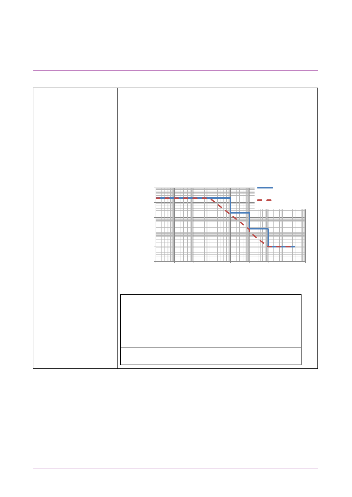
*2: Post-cursor:
*3: Typical value
, Pre-cursor:
1-35
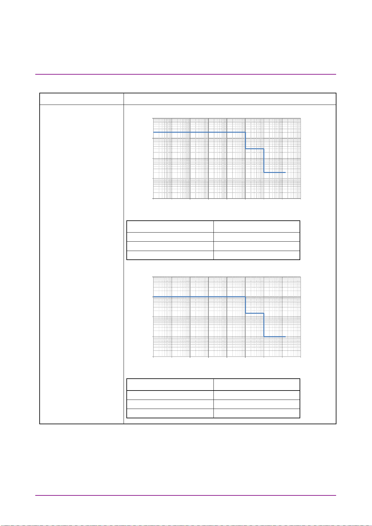
Page 52

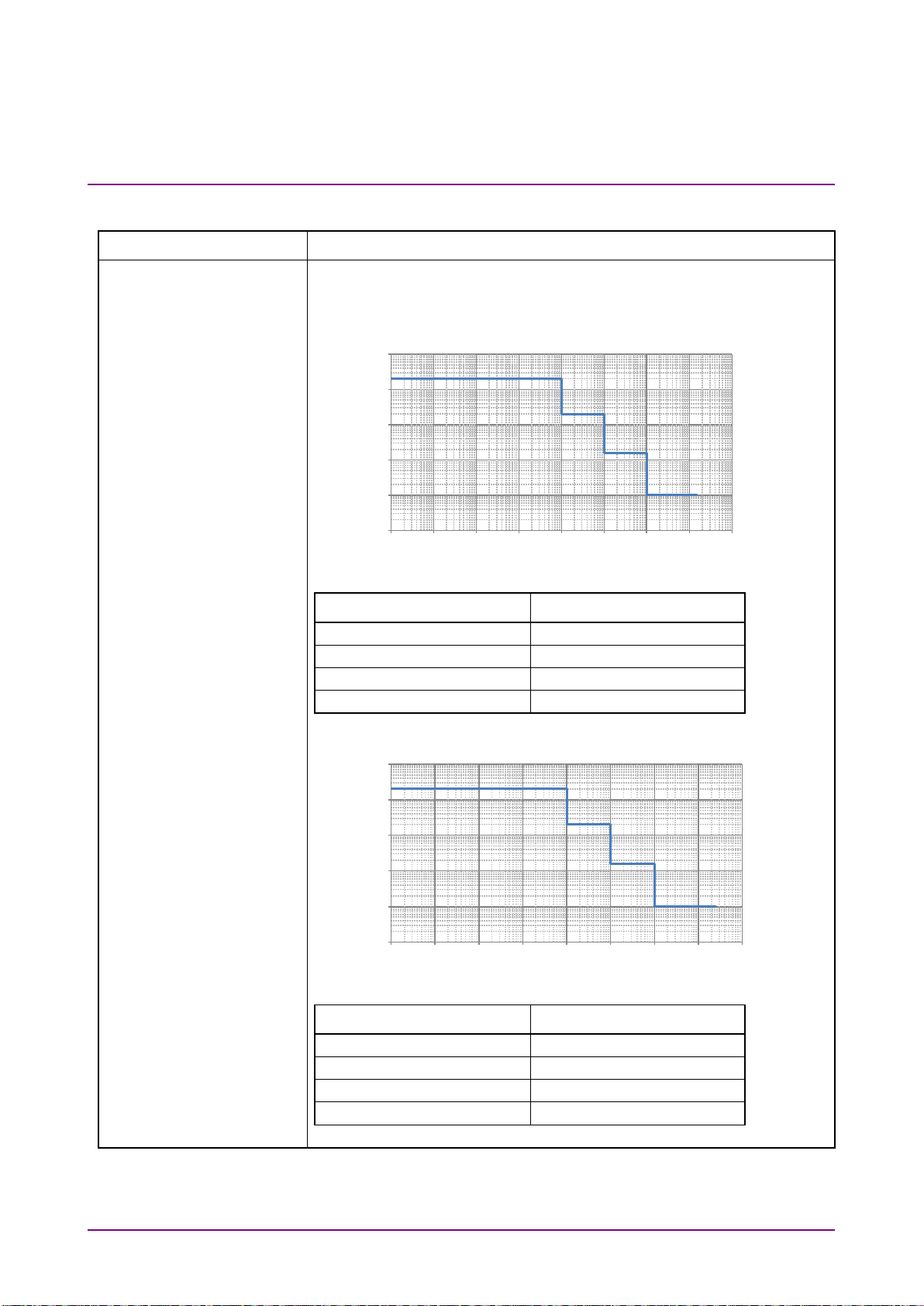
0
5
10
15
20
25
30
35
0 0.2 0.4 0.6 0.8 1 1.2 1.4
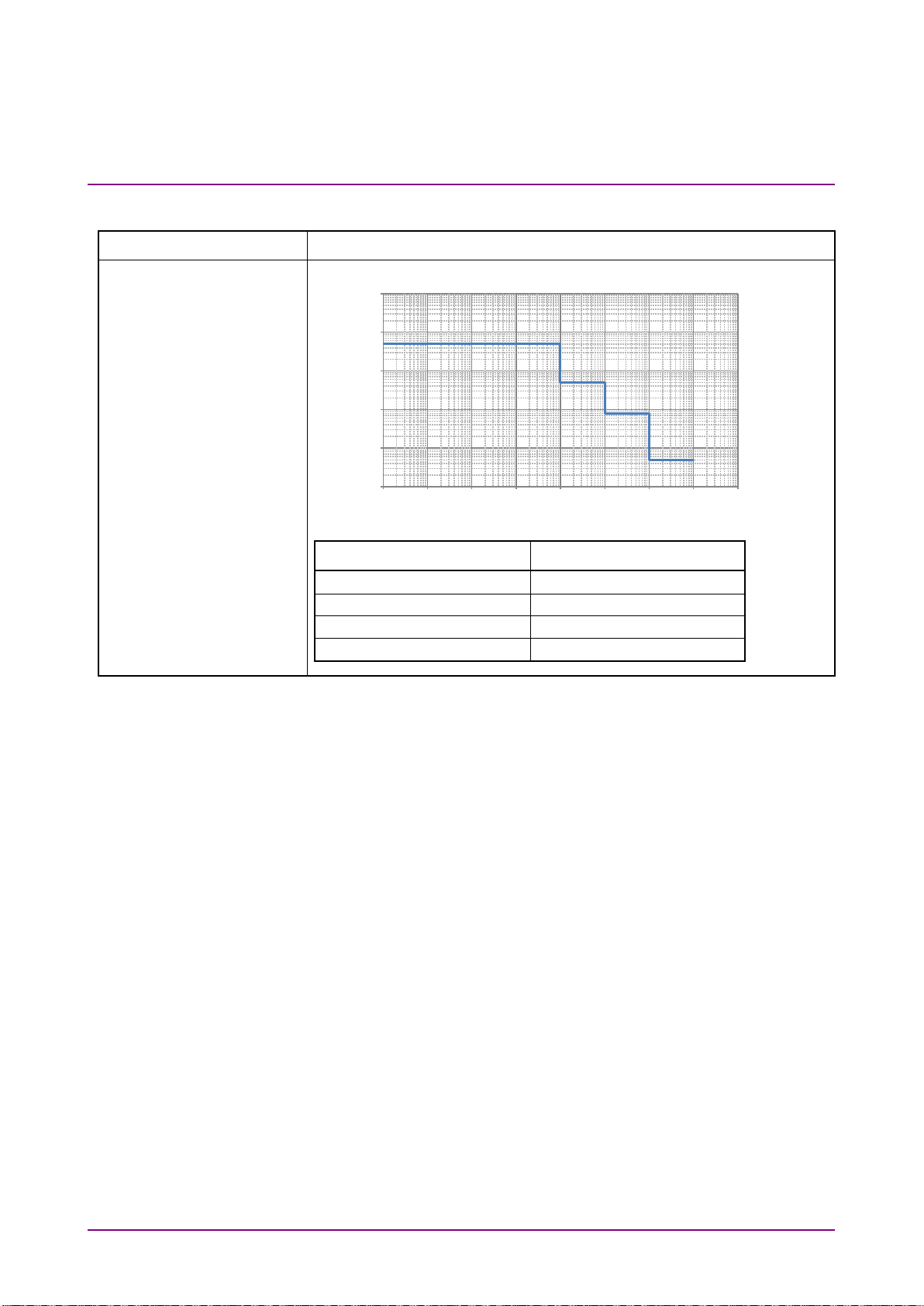
Compensatable Insertion loss (dB)
Amplitude (V)
Normalized Frequency
0 0.1 0.2 0.3 0.4 0.5
0
-5
-10
-15
-20
-25
-30
Insertion Loss (dB)
Setting
Ideal
Chapter 1 Overview
*4: Defined for the preset of 8 Gbit/s, 16 Gbit/s, and 25 Gbit/s for PCIe 3
and PCIe 4 respectively.
*5: Maximum time to transition to valid diff signaling after leaving
Electrical Idle
*6: When Option x40 or Option x41 is installed.
*7: The compensable maximum transmission line loss without
decreasing the amplitude by the Channel Emulator function is
shown in the following graph.
1-36
*8: The frequency characteristics of Insertion Loss Accuracy when
setting 25 dB@Nyquist Frequency and 12.5 dB@1/2 Nyquist
Frequency are shown below. (Nominal)
Page 53

Overview
Table 1.3.1-13 Clock Output
Frequency
Full Rate
2.4 to 21.0 GHz*2
Operation bit rate is same as clock output frequency.
Half Rate
1.2 to 10.5 GHz*2
Operation bit rate is double of output clock frequency.
Number of Output
1
Amplitude
0.3 to 1.0 Vp-p
Output control
ON, OFF switching
Termination
AC, 50 Ω
Connector
K (f.)
Phase setting range
–1000 to +1000 mUI, in 2 mUI steps
Accuracy
±50 mUIp-p*2,*3
mUI – ps switching
Available
Calibration
Available
Calibration indicator
This indicator is on when Calibration is required due to:
• Ambient temperature change by ±5 degree.
Item Specifications*
2.4 to 32.1 GHz*3
1.2 to 16.05 GHz*3
*1: These values are monitored using an applicable part (J1439A coaxial
cable, 0.8 m, K connector) at a sampling oscilloscope bandwidth of 70
GHz.
1.3 Specifications
1
1
*2: Option x01 not available.
*3: Option x01 available.
1
Table 1.3.1-14 Data Delay*
Item Specifications
• 1/1 Clock frequency change by ±250 kHz.
*1: When Option x30 or Option x31 is available.
*2: When using an item with an oscilloscope residual jitter of less than
200 fs (RMS).
*3: Typical value
1-37
Page 54
Jitter tolerance mask
Bit rate: 16 Gbit/s, 28.1 Gbit/s*, 32.1 Gbit/s*
10
2,000
2,000
7,500
2,000
2,000
100,000
2,000
150
1,000000
200
15
10,000,000
16
1
250,000,000 1 1
Jitter Amplitude [UI]
Chapter 1 Overview
Item Specifications
Table 1.3.1-15 Jitter tolerance
Pattern: PRBS231–1
SSC with a 5300 ppm amplitude and RJ of 0.3 UI can be
simultaneously applied by using MU181500B.
These specifications are defined assuming the following conditions:
Loopback connection to the MU195040A, defined by one specific
temperature in the range of 20 to 30°C.
When RJ + BUJ is bigger than 0.5 UIp-p or SJ1 + Built-in SJ2 + RJ +
BUJ is bigger than the standard value + 0.3 UIp-p, “Overload” is
displayed on the MU181500B screen.
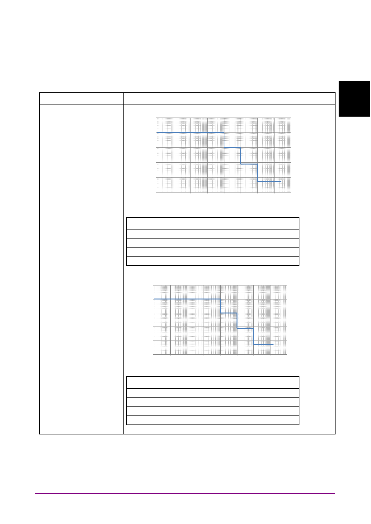
10000
1000
100
MAX. modulation
amplitude
Specification
frequency [Hz]
*: Option x01 available.
Modulation
10
1
0.1
10 100 1k 10k 100k 1M 10M 100M 1000M
Modulation Frequency [Hz]
MAX. modulation
amplitude [UIp-p]
Specification [UIp-
p]
1-38
Page 55

Overview
Table 1.3.1-16 Multichannel operation*1
Combination Setting *2
2ch Combination
• Combination using multiple modules is not supported. .
Channel Synchronization
Generate patterns that start position has been synchronized as a
Image of Channel Synchronization
3 5 7
2 4 6 8
1 2 3
4
Data1
1
2 3 4
Data2
1.3 Specifications
Item Specifications
Generates signals with bit phase shift as 42/64 Gbit/s band signal
source.
Supports 2ch Combination.
Data1
Data2
Image of 2ch Combination
Combination condition:
parallel signal generator.
Each channel has an independent Test Pattern and is controlledso that
the timing of generation in the same.
*1: Multichannel operation cannot be set when Test Pattern is set to
Sequence.
1
1
*2: Option x31 is required.
1-39
Page 56

Inter-modules
• When modules to be combined are installed sequentially from slot 1.
2ch CH Sync*4
Inter-modules synchronization of 2ch Combination:
Image of 2ch CH Sync
CH Sync
Inter-modules synchronization:
Image of CH Sync
64G × 2ch
Inter-modules synchronization of 2ch Combination:
Image of 64G × 2ch Combination
Slot2
Slot1
1 5 9
13
Data1
3 7 11
15
Data2
2 6 10
14
Data1
4 8 12
16
Data2
1 2 3 4 Data1
1 2 3 4 Data2
1 2 3 4 Data1
1 2 3 4 Data2
Slot2
Slot1
3
6 8
1 3 5 7
2 4 6 8
Slot2
Slot1
Chapter 1 Overview
Item Specifications
Table 1.3.1-16 Multichannel operation (Cont’d)
combination*3
Combination Setting condition:
• Options of each module must be same.
• Slot 1 to 4: 2ch CH Sync, CH Sync, 64G × 2ch Combination
DataXs of each module synchronize.
Data1
Data2
1
2
5 7
4
Data1
Data2
Pattern bits of each Data channel synchronize.
Combination*4
Pattern bits of DataX channel of each module shift in 1/4 period.
*3: Option x30 or option x31 is required.
*4: Only for option x31.
1-40
Page 57

Overview
Table 1.3.1-16 Multichannel operation (Cont’d)
Output
Phase variable range
–64 000 to +64 000 mUI*5
Phase variable step
2 mUI*5
Pattern
Data
Data Length
2 × n to 268435456 × n bits, in n-bit steps*6
Mixed
Row Length
(2048 × n) to {(268435456 +231) × n}, in (1024 × n)-bit steps*6
Data Length
(1024 × n) to 268435456 × n bits, in n-bit steps*6
Burst
Burst Cycle
(25600 × n) to (2147483648 × n) bits, in (1024 × n)-bit steps*6
Enable period
Internal:
Ext Trigger:
(12800 × n) to 2147483392 × n bits, in (256 × n)-bit steps*
(12800 × n) to 2147483648 × n bits, in (256 × n)-bit steps*6
Pulse Width
0 to {(Burst Cycle – 128) × n} bits, in (8 × n)-bit steps*6
Delay
0 to {(Burst Cycle – 128) × n} bits, in (8 × n)-bit steps*6
Gating Output Repeat
(Data)
Pulse Width
0 × n to (268435328 × n), in (8 × n)-bit steps*6
Delay
0 × n to (268435328 × n), in (8 × n)-bit steps*6
Repeat (Mixed)
Pulse Width
0 × n to (231 + 268435456 – 128) × n, in (8 × n)-bit steps*6
Delay
0 × n to (231 + 268435456 – 128) × n, in (8 × n)-bit steps*6
Dimensions
21 mm (H), 234 mm (W), 175 mm (D) Excluding protrusions
Mass
2.5 kg max.
Operating Temperature
15 to 35°C
Storage Temperature
–20 to 60°C
1.3 Specifications
Item Specifications
1
6
*5: A separate value can be set for each channel. This value is common
to both Channel Combination and Channel Synchronization.
*6: Common to every channel specified by Combination Setting.
Table 1.3.1-17 General
Item Specifications
1-41
Page 58

PCIe
Supports the following PCIe tests when controlled by MX183000A.
Supported standards
PCI Express Base Specification Revision 4.0 Version 0.5, 0.7, 1.0
Test target: Root Complex, End Point
Required option
Option x10/x11 or x20/x21
Required software
MX183000A-PL011:
supporting Jitter Tolerance Test.
Loopback Through
Configuration, Recovery
Test pattern
Modified Compliance Pattern
Generation”)
SKP Ordered Set
Insertion
Enable, Disable
SKP Length/Insertion
For Gen1, Gen2
Interval: 187 to 750, 1-steps
Dynamic Link Training
Available when using MX183000A-PL021.
Ling training repeat
1 to 15 (when using MX183000A-PL021)
Chapter 1 Overview
Item Specifications
Table 1.3.1-18 Extension Function
PCI Express Base Specification Revision 5.0 Version 1.0
Bitrate: PCIe Gen1, Gen2, Gen3, Gen4, Gen5
Lane number: × 1
This software enables setting DUT to Loopback state
by following PCIe LTSSM and generating a training
sequence required for transition to Loopback state.
MX183000A-PL021:
This software enables setting DUT to Loopback state
by following PCIe LTSSM and supporting negotiation
with DUT. LTSSM state transition can be analyzed as
log. (With this software, one MU195020A and one
MU195040A are required.)
MX183000A-PL025:
This software enables extending the functionality of
PL021 to PCIe 5.0.
Adding MX183000A-PL001 to each option of the above software
enables controlling MU195020A, MU181500B, and MU195040A and
Insert Delay Symbol: Enable, Disable (Available for Gen1 and
Insert SRIS: Enable, Disable (Available for Gen3,
Compliance Pattern
Insert Delay Symbol: Enable, Disable (Available for Gen1 and
User
PRBS, Data (8. The pattern defined in Table 1.3.1-6 “
Length: COM+1, COM+2, COM+3, COM+4, COM+5
Interval: 768 to 3076, 1-steps
For Gen3, Gen4, Gen5
Length: 8, 12, 16, 20, 24
Gen2)
Gen4, and Gen5)
Gen2)
Pattern
1-42
Page 59

Overview
Table 1.3.1-18 Extension Function (Cont’d)
Counter
Tx SKP Count,
Error Rate, Error Count (when using MX183000A-PL021)
Error Addition
Defined for Modified Compliance Pattern, Compliance Pattern
Error Variation
Repeat, Single
Error Ratio
*E– n (*=1 to 9, n=3 to 12), upper limit is 5.0E–3.
PAM4
Supports the following by combining MU195020A with MZ1834A/B
• Emphasis Peak Voltage (Single-ended) 0.3 to 2.25 Vp-p (G0375A)
USB
Supports the following USB tests when controlled by MX183000A.
Supported standards
USB3.0/3.1
Required option
Option x10/x11 or x20/x21
Required software
MX183000A-PL022:
supporting Jitter Tolerance Test.
1.3 Specifications
Item Specifications
Rx SKP Count (when using MX183000A-PL021)
and G0375A.
PAM4 signal generation
• Amplitude (Single-ended) 0.048 to 0.310 Vp-p (MZ1834A)
• Amplitude (Single-ended) 0.048 to 0.489 Vp-p (MZ1834B)
• Amplitude (Single-ended) 0.3 to 1.95 Vp-p (G0375A)
PAM4 Emphasis signal generation (when Option x11 or Option x21 is
installed)
• Emphasis Peak Voltage (Single-ended) 0.048 to 0.357 Vp-p
(MZ1834A)
• Emphasis Peak Voltage (Single-ended) 0.048 to 0.564 Vp-p
(MZ1834B)
1
This software enables setting DUT to Loopback state by
following USB LTSSM and supporting negotiation with DUT.
LTSSM state transition can be analyzed as log. (With this
software, one MU195020A and one MU195040A are required.)
Adding MX183000A-PL001 to each option of the above software
enables controlling MU195020A, MU181500B, and MU195040A and
1-43
Page 60

Operating bit rate
2.4 to 21.0 Gbit/s*1
2.4 to 32.1 Gbit/s*2
System Clock
External, Clock Recovery, Clock and Data Recovery are optional.*
Number of inputs
2 (Data, XData) (Differential)*1
4 (Data1, XData1, Data2, XData2) (Differential)*2
Amplifier
Single-Ended 50 Ω, Differential 50 Ω, Differential 100 Ω can be set.
CTLE: On/Off Switching*4
Input signal format
NRZ, PAM4
Input amplitude*5
0.05 to 1.0 Vp-p (NRZ)
0.4 to 1.0 Vp-p (PAM4, > 28.1 Gbaud)
Threshold voltage
–3.5 to +3.3 V (1mV step) (Can be set separately.)
shall be 3 V or less.)
Chapter 1 Overview
1.3.2 Specifications for MU195040A
Table 1.3.2-1 Operating bit rate
Item Specifications
*1: When option x01 is not installed.
*2: When option x01 is installed.
Table 1.3.2-2 System Clock
Item Specifications
*: Available when Option x22 is installed. If it is not installed, only
External is available. Clock is recovered from the data input to the
Data1 Input connector.
Table 1.3.2-3 Data Input
Item Specifications
At single-ended 50 Ω: Data and XData can be set.
At differential 50/100 Ω: Tracking, Independent, Alternate can be set.
When Alternate is selected:
Data-XData and XData-Data can be set.*
0.3 to 1.0 Vp-p (PAM4, ≤ 28.1 Gbaud)
(Absolute value of difference between Data and XData Threshold values
*1: Option x10
*2: Option x20
3
*3: Absolute value of difference between Data and XData Threshold
values shall be 1.5 V or less.
*4: Option x11 or Option x21
*5: The NRZ input amplitude is the range where the Auto Adjust
function operates. The PAM4 input amplitude is the range where the
1-44
PAM4 Auto Search function operates. Input sensitivity is the
minimum input amplitude which becomes error-free.
Page 61

Overview
Table 1.3.2-3 Data Input (Cont’d)
Input sensitivity
NRZ*5,*6,*7
21.0 Gbit/s
28.1Gbit/s*8
Amplitude
19 mVp-p*9, ≤27 mVp-p
22 mVp-p*9, ≤31 mVp-p
Eye height*10
13 mV*9
15 mV*9
PAM4*5,*7,*11
21.0 Gbaud
28.1 Gbaud*8
Amplitude
120 mVp-p*9, 40 mV/Eye
150 mVp-p*9, 50 mV/Eye
Eye height
24 mV*9
26 mV*9
Eye Height
MP1900A
MU195020A
MU195040A
ATT
Data Output
Data Input
Amplitude
1.3 Specifications
Item Specifications
Bitrate
Baud rate
*6: PRBS31, Single-Ended, Mark ratio 1/2, CTLE OFF
*7: Defined by one specific temperature in the range of 20 to 30°C.
*8: Option x01
*9: Typical value
*10: Sensitivity of eye height.
Eye height is the minimum value that induces no bit error when
MU195040A receives the output signal from MU195020A + ATT in
the measurement system shown in the following figure (using a
sampling oscilloscope of 70 GHz band or higher for measuring
output amplitude).
1
*11: PRBS15, Single-Ended, marking rate equivalent to 1/2, CTLE OFF,
MU195020A + G375A and back-to-back connection
1-45
Page 62
Phase margin
NRZ*6,*12
25.0
28.1
32.1
Phase margin
33 ps*9
27 ps*9
20 ps*9
18 ps*9
25.0
Gbaud*8
28.1
Gbaud*8
32.1
Gbaud*8
Phase margin
13 ps*9
8 ps*9
5 ps*9
2 ps*9
Eye width
26.5 ps*9
20 ps*9
15 ps*9
13 ps*9
21.0 Gbaud
25.0 Gbaud*8
28.1 Gbaud*8
Phase margin
8 ps*9
5 ps*9
3 ps*9
Eye width
26.5 ps*9
20 ps*9
15 ps*9
Termination
GND,50 Ω,
Variable,50 Ω
Termination voltage
When Variable is selected for Termination: –2.5 to +3.5 V, 10 mV step
Connector
K (f.)
CTLE*4
Band
OFF, 8-10 Gbit/s, 16-20 Gbit/s, 25-28 Gbit/s, PCIe3, PCIe4, PCIe5
CTLE Gain
Setting range
0 to –12 dB, 0.1 dB step
Accuracy
±0.5 dB*9
Input amplitude
0.05 to 0.4 Vp-p*14
Chapter 1 Overview
Item Specifications
Table 1.3.2-3 Data Input (Cont’d)
Bitrate
21.0 Gbit/s
PAM4 Middle*
11,*13
21.0 Gbaud
PAM4 Upper/Lower*
11,*13
Gbit/s*8
Gbit/s*8
Gbit/s*8
Baud rate
Baud rate
*12: When using 0.5 Vp-p Input and External Clock.
*13: Emphasis ON (Best value in the range of 1Pre ≤ 3 dB/1 Post ≤ 1 dB),
Based on the IEEE802.3bs measurement methods
*14: Input range that the signal is not saturated when CTLE is On.
1-46
Page 63

Overview
Table 1.3.2-4 Clock Input
Number of inputs
1 (Single-Ended)
Frequency range
1.2 to 16.05 GHz
Input level
0.3 to 1.0 Vp-p (–6.5 to +4.0 dBm)
Termination
AC, 50 Ω
Connector
SMA (f.)
Aux Input
Number of inputs
1 (Single-Ended)
Variation
External Mask, Burst, Capture External Trigger
Minimum pulse width
1/128 of Data rate
Input level
• 0/–1 V (H: –0.25 to 0.05 V / L: –1.1 to –0.8 V)
Select one of the above.
Termination
GND, 50 Ω
Connector
SMA (f.)
Aux Output
Number of outputs
2 (Differential)
Variation
1/n Clock (n = 4, 6, 8, 10…510, 512), Pattern Sync*, Sync. Gain, Error
Output
Pattern Sync
PRBS, PRGM
Position: 1 to {(Least common multiple of Pattern Length’ and 128) –
Length setting until it becomes 512 or more if it is 511 or less.
Mixed Data
Block No. setting:
Output level
0/–0.6 V (H: –0.25 to 0.05V / L: –0.80 to –0.45 V)
Termination
GND, 50 Ω
Connector
SMA (f.)
1.3 Specifications
Item Specifications
Table 1.3.2-5 Aux Input, Aux Output
Item Specifications
• 0/–0.5 V (H: –0.05 to 0.05 V / L: –0.55 to –0.45 V)
• Vth 0 V (Input amplitude 0.5 to 1.0 Vp-p)
1
135}, in 8-bit steps
Pattern Length’ shall be the value obtained by multiplying Pattern
1 to the Block No. specified for Mixed Data, in 1-steps
Row No. setting:
1 to the Row No. specified for Mixed Data, in 1-steps
*: Cannot be selected when Test Pattern is HSSB Data.
1-47
Page 64

PRBS
Pattern length
2n–1 (n = 7, 9, 10, 11, 13, 15, 20, 23, 31)
Mark ratio
1/2 (1/2INV is supported by a logical inversion.)
Zero-Substitution
Additional Bit
0 bit, 1 bit
Pattern length
2n or 2n–1 (n = 7, 9, 10, 11, 15, 20, 23)
Start position
Substitutes the bit coming after the maximum “0” successive bits.
Successive-zeros bit
1 to (Pattern Length–1) bits
Data Data length
2 to 268435456 bits, in 1-bit steps
Mixed Pattern
Pattern
Data
Mixed Block
To the smaller of the following values:
× lengthData
countROW
268435456
INT
× countROW
lengthROW
2+268435456
INT
31
Mixed Row Length
2048 to 268435456+231 bits, in 1024-bit steps (Data + PRBS Length)
Data length
1024 to 268435456 bits, in 1-bit steps
Number of rows
1 to 16, in 1-steps
Number of blocks
1 to 511, in 1-steps
PRBS steps/Mark ratio
Same as PRBS.
PRBS Sequence
Restart, Consecutive
Descramble
Can be set per PRBS and Data for each Block (except the Data area for
Block 1).
PAM4 *1
Pattern Type
Square Wave, JP03A, JP03B, PRQS10, SSPR, QPRBS13,
User Define
User Define in detail
Raw Data
PRBS, Data
PRBS Pattern Length
Same as PRBS.
PRBS Inversion
Logic Inversion/Non-Inversion of PRBS part
Data Length
Same as Data
Gray Coding
Gray Coding ON/OFF
Chapter 1 Overview
Item Specifications
Table 1.3.2-6 Pattern Detection
length
If the bit coming after Zero-substitution is “0,” then it is replaced with
“1.”
1 to 511 Block, in 1-Block steps
bits
bits
QPRBS13-CEI, SSPRQ, Transmitter Linearity, PRBS13Q, PRBS31Q,
*1: Configurable when 2ch Combination is set
1-48
Page 65

Overview
Table 1.3.2-6 Pattern Detection (Cont’d)
HSSB Data*2
Specification
PCIe1, PCIe2, PCIe3, PCIe4, USB3.0, USB3.1 Gen2
EIEOS
EIEOS Insertion: ON,OFF
Insertion.
SYNCOS
SYNC OS Insertion: ON, OFF
Enabled when Specification is USB3.1 Gen2.
Scrambler Seed
When Specification is set to PCIe1, PCIe 2, or USB3.0: FFFF
When Specification is set to USB3.1 Gen2: 1DBFBC
PCIe1
Length
32 to 1024 bit, 8bit step
Coding
8b10b
PCIe2
Length
32 to 1024 bit, 8bit step
Coding
8b10b
PCIe3
Length
128 to 1024 bit, 128bit step
Coding
128b130b
PCIe4
Length
128 to 1024 bit, 128bit step
Coding
128b130b
USB3.0
Length
32 to 1024 bit, 8bit step
Coding
8b10b
USB3.1 Gen2
Length
128 to 1024 bit, 128bit step
Coding
128b132b
1.3 Specifications
Item Specifications
EIEOS Interval: 1 to 65536 pattern repeats, 1 step
Enabled when Specification is PCIe1, PCIe2, PCIe3, and PCIe4
When Specification is PCIe3 or PCIe4, only ON is available for EIEOS
SYNC OS Interval: 1 to 65536 pattern repeats, 1 step
When Specification is USB3.0, only OFF is available.
When Specification is set to PCIe3, or PCIe4:
Lane0, Lane1, Lane2, Lane3, Lane4, Lane5, Lane6, Lane7
1
*2: This can be set only when Module Combination is set to Independent
and the channel is Data1.
1-49
Page 66

HSSB Data*2 (Cont’d)
8b10b Pattern Editor
Notation
Symbol, Bin, Hex
Scrambler Enable
Scrambles the selected symbols.
ON, OFF
Scrambler Reset
Resets the seed value of scrambler on the selected symbols.
ON, OFF
Code
K-code, D-code
K code
K28.0, K28.1, K28.2, K28.3, K28.4, K28.5, K28.6, K28.7
K23.7, K27.7, K29.7, K30.7
D code
D0.0 to D31.7
MSB First / LSB First
MSB First, LSB First
128b130b Pattern Editor
Notation
Bin, Hex
Scrambler Enable
Scrambles the selected symbols.
ON, OFF
Scrambler Reset
Resets the seed value of scrambler on the selected symbols.
ON, OFF
DC Balance
Adds DC balance to the symbol 14 and 15.
ON, OFF
Sync Header
Defines 2-bits Sync Header.
MSB First / LSB First
MSB First, LSB First
128b132b Pattern Editor
Notation
Symbol Bin, Symbol Hex
Scrambler Enable
Scrambles the selected symbols.
ON, OFF
Scrambler Reset
Resets the seed value of scrambler on the selected symbols.
ON, OFF
DC Balance
Adds DC balance to the symbol 14 and 15.
ON, OFF
Sync Header
Defines 4-bits Sync Header.
MSB First / LSB First
MSB First, LSB First
Chapter 1 Overview
Item Specifications
Table 1.3.2-6 Pattern Detection (Cont’d)
1-50
Page 67

Overview
Table 1.3.2-7 Pattern Sequence
Sequence
Repeat, Burst
Repeat
Continuous Pattern
Burst
Source
Internal, External-Trigger (Aux Input), External-Enable (Aux Input)
Delay
Internal: 0 to 2147483640 bits, in 8-bit steps
Adjust Method: Auto, Manual
Enable Period
Internal: 12800 to 2147482624 bits, in 256-bit steps
Ext Trigger: 12800 to 2147483392 bits, in 256-bit steps
Burst Cycle
25600 to 2147483648 bits, in 1024-bit steps
1.3 Specifications
Item Specifications
Ext Trigger, Enable: 0 to 2147483520 bits, in 8-bit steps
1
1-51
Page 68

Measurement types
Error Rate: 0.0001E–18 to 1.0000E00
Clock Loss Interval: 0 to 9999999, 1.0000E07 to 9.9999E17
Gating
Time, Clock Count, Error Count, Block Count
Unit, Cycle setting
Time: 1 second to 99 days 23 hours 59 minute 59
Block Count: > E+2 to > E+14
Gating Cycle
Single, Repeat, Untimed
Current
On, Off can be set.
Interval: 100 ms, 200 ms, 500 ms
Auto Sync
On, Off can be set.
INT, E–2 to E–8
Sync Control
PRBS: Automatic Synchronization
HSSB Data: Automatic Synchronization
Frame length
4 to 64 bits, in 4-bit steps
Frame mask
Available
Frame Position
1 to (Pattern Length – Frame Length +1) bits, in 1-bit steps
Error/Alarm conditions
Error detection mode
• Total, Insertion, Omission
• Transition, Non Transition
EI/EFI interval
1 ms, 10 ms, 100 ms, 1 s
SKP OS Filtering
Filters the SKP OS that are compliant with the following standards:
When Test pattern is HSSB Data, only ON is enabled.
Chapter 1 Overview
Item Specifications
Table 1.3.2-8 Measurement
Error Count: 0 to 9999999, 1.0000E07 to 9.9999E17
Error Interval: 0 to 9999999, 1.0000E07 to 9.9999E17
%Error Free Interval: 0.0000 to 100.0000
Frequency: 2400.000 to 32100.000 MHz
Frequency measurement accuracy:
±1 ppm ±1 kHz*
Clock Count: 0 to 9999999, 1.0000E07 to 9.9999E17
Sync Loss Interval: 0 to 9999999, 1.0000E07 to 9.9999E17
seconds
Clock Count: > E+4 to > E+16
Error Count: > E+4 to > E+16
Calculation: Progressive, Immediate
Synchronization threshold:
Data: Frame On, Quick
Mixed-Data: Frame On
• PCIe: Gen1, Gen2, Gen3, Gen4, Gen5
This function is available only at the bit rate of each standard.
*: When Gating is selected and the MP1900A reference clock 10 MHz is
calibrated.
1-52
Page 69

Overview
Table 1.3.2-9 Error Analysis
Block Window
Excludes the specified data pattern bit from the measurement target
Pattern.
Setting resolution
Pattern length (bits)
134217729 to 268435456
Step [bits]
128
Bit window*1
Excludes any channels among internal 32 channels from the
External mask*1
H: Measurement
L: Mask
Capture function*1
Number of blocks
1, 2, 4, 8, 16, 32, 64, 128
Length of block
n
Mbits8
Trigger
Error Detect, Match Pattern, Manual Trigger, External Trigger (Rising
Edge)
Trigger position
Top, Middle, Bottom
Matching pattern
4 to 64, in 4-bit steps
Automatic measurement
function
Eye margin*1,*2, Bathtub*1,*2, Eye Contour*1,*2, PAM4 BER
measurement
Auto Adjust*3,*4,*5, Auto Search*3, Auto Search PAM4 mode*6
1.3 Specifications
Item Specifications
according to the settings.
Invalid when “Mixed” pattern or “HSSB Data” is selected for Test
2 to 2097152
2097153 to 4194304
4194305 to 8388608
8388609 to 16777216
16777217 to 33554432
33554433 to 67108864
67108865 to 134217728
measurement target.
(n is Number of blocks.)
1
1
2
4
8
16
32
64
*1: Not available when “HSSB Data” is selected for Test Pattern.
*2: Unavailable when the system clock is set to Clock and Data
Recovery.
*3: The input pattern must be an NRZ PRBS pattern with a mark ratio
of 1/2.
*4: The Auto Adjust function obtains a point in the vicinity of the
following as an optimum point:
• (Voh + Vol) / 2 in voltage direction
• (P1 + P2) / 2 in phase direction
The Auto Adjust function works properly when there are no maskhits which are observed by the oscilloscope vertically within ±25 mV
area from the Auto Adjust operating point.
1-53
Page 70

PAM4 BER Measurement
Available patterns
• Transmitter_Linearity
Voh
Auto adjust operating point
P1
P2
Vol
25mV
Chapter 1 Overview
Item Specifications
*5: If eye diagram of input signal is not symmetry, the Auto Adjust may
not adjust input signals to the optimum value. The Auto Search Fine
is recommended to measure asymmetric input signals.
*6: Each of PAM4 waveform levels is equal. PRBS pattern with a mark
ratio of 1/2.
Table 1.3.2-10 PAM4 BER Measurement
• GrayPRBS7, 9, 10, 11, 13Q-IEEE200G_400G[Draft2], 15,20
• GrayPrePRBS20
• GrayPreQPRBS13-CEI
• GrayPreQPRBS13-IEEE100GBASE-KP4_Lane0, 1, 2, 3
• GrayPRQS10
• GrayQPRBS13-CEI
• GrayQPRBS13-IEEE100GBASE-KP4_Lane0, 1, 2, 3
• GraySSPR
• PRBS7, 9, 10, 11, 13Q-IEEE200G_400G[Draft2], 15, 20
• PrePRBS20
• PreQPRBS13-CEI
• PRQS10
• QPRBS13-CEI
• QPRBS13-IEEE100GBASE-KP4_Lane0, 1, 2, 3
• Squarewave
• SSPR
• SSPRQ
1-54
Page 71

Overview
Table 1.3.2-11 Variable Clock Delay
Phase variable range
–1000 to +1000 mUI, 2 mUI step
Accuracy
±50 mUIp-p*1,*2
mUI – ps switching
Available
Calibration
Available
Calibration indicator
This indicator is on when Calibration is required due to:
• Change in the ambient temperature by ±5°C.
Clock source options
Clock Recovery, Clock and Data Recovery Clock*1
Operating bit rate
2.4 to 21.0 Gbit/s*
2.4 to 21.0 Gbaud*
28.100 001 to 32.1 Gbaud*3,*4
Setting range
2.400000 to 21.000000 Gbit/s, 0.000001 Gbit/s step*
2
2.400000 to 32.100000 Gbit/s, 0.000001 Gbit/s step*3
1.3 Specifications
Item Specifications
• Change in 1/1Clock frequency by ±250 kHz.
*1: Using oscilloscope with residual jitter of less than 200 fs (RMS).
*2: Typical value
Table 1.3.2-12 Clock Recovery
Item Specifications
NRZ PAM4
2
2.4 to 32.1 Gbit/s*3
2.4 to 28.1 Gbaud*3
1
2
*1: The system clock can be selected only when option x22 is installed.
Clock is recovered from the data input to the Data1 Input connector.
The input pattern must be an NRZ PRBS pattern with a mark ratio
of 1/2.
When PAM4 is set, clock recovery is performed with PRBS15, Data1
and Middle. Upper, Middle, Lower are measured with Data2.
At the back-to-back connection with MU195020A + J1741A +
G0375A + J1728A, the target loop band is defined at the maximum
bit rate of each Bit rate range.
*2: When option x22 is installed.
*3: When option x01 is installed.
*4: Typical value, BER 1.0E–7
1-55
Page 72
Supported standard and
Standard
Bit rate [Gbit/s]
100G ULH
32.100000*3
PCI Express Gen5
32.000000*3
32GFC
28.050000*3
100G OTU4
27.952496*3
100GbE(25.78x4)
25.781250*3
InfiniBand EDR
25.781250*3
SAS
24.000000*3
SAS4
22.500000*3
Thunderbolt2
20.625000
DisplayPort UHBR 20
20.000000
USB4 Gen3
20.000000
PCI Express Gen4
16.000000
InfiniBand FDR
14.062500
16G FC
14.025000
DisplayPort UHBR 13.5
13.500000
10G FC Over FEC
11.316800
10GbE Over FEC
11.095700
OTU2
10.709225
G975 FEC
10.664228
10G FC
10.518750
10GbE
10.312500
Thunderbolt1
10.312500
DisplayPort UHBR 10
10.000000
USB4 Gen2
10.000000
InfiniBand QDR
10.000000
USB3.1
10.000000
OC-192/STM-64
9.953280
8G FC
8.500000
DisplayPort HBR3
8.100000
PCI Express Gen3
8.000000
HSBI
6.250000
SATA 6Gb/s
6.000000
DisplayPort HBR2
5.400000
PCI Express Gen2
5.000000
USB3.0
5.000000
InfiniBand DDR
5.000000
4G FC
4.250000
Chapter 1 Overview
bit rate
Table 1.3.2-12 Clock Recovery (Cont’d)
Item Specifications
1-56
Page 73

Overview
Table 1.3.2-12 Clock Recovery (Cont’d)
Supported standard and
Operating bit rate tracking
Supported.
same mainframe
Maximum number of
consecutive zeros*5
72 bit (Zero Substitution 215)
Lock range*5
±200 ppm
Target loop band
1667
rateBit
2578
rate
Bit
Standard
Bit rate [Gbit/s]
XAUI
3.125000
SATA 3Gb/s
3.000000
DisplayPort HBR
2.700000
OTU1
2.666060
InfiniBand SDR
2.500000
PCI Express Gen1
2.500000
OC-48/STM-16
2.488320
2.400000 to 5.500000
3
-
5.500001 to 7.500000
3 to 4
1
7.500001 to 9.500000
3 to 5
1
9.500001 to 10.500000
3 to 6
1
10.500001 to 12.500000
3 to 7
1
12.500001 to 14.500000
3 to 8
1
14.500001 to 15.500000
3 to 9
1
15.500001 to 17.500000
3 to 10
1
17.500001 to 19.500000
3 to 11
1
19.500001 to 20.500000
3 to 12
1
20.500001 to 22.500000
3 to 13
1
22.500001 to 24.500000
3 to 14
1
24.500001 to 25.500000
3 to 15
1
25.500001 to 27.500000
3 to 16
1
27.500001 to 29.500000
3 to 17
1
29.500001 to 30.500000
11 to 18
1
30.500001 to 32.100000
11 to 19
1
1.3 Specifications
Item Specifications
bit rate (Cont’d)
Tracking target: The operating bit rate of the PPG mounted to the
Available options are
Tolerance*
If the Variable option is selected, the following settings are available:
6
and Variable.
Bit rate [Gbit/s] Setting Range [MHz] Step [MHz]
MHz,
MHz, Jitter
1
*5: When the option x22 is installed:
The target loop band is specified by the maximum setting value of
each bit rate.
*6: The Jitter Tolerance option makes the loop band wider than the
other options and enables the Jitter Tolerance measurement.
1-57
Page 74
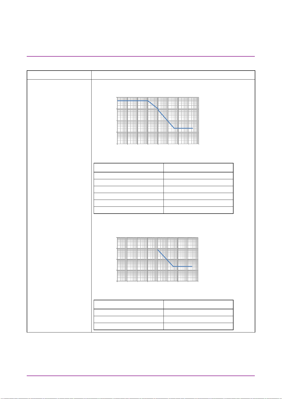
Jitter Tolerance
At the bit rate of 28.05 Gbit/s, conforming to Jitter Tolerance Mask
10
50
10,000
50
100,000
10
108,805
7.5
3,709,271
0.22
250,000,000
0.22
100,000
7.5
3,409,256
0.22
250,000,000
0.22
Jitter Amplitude [UI]
Jitter Amplitude [UI]
Chapter 1 Overview
Item Specifications
Table 1.3.2-12 Clock Recovery (Cont’d)
Clock Recovery*7,*8
defined by the “32G FC standard”
100
10
1
0.1
0.01
10 100 1k 1 0k 100k 1M 10M 100M 1 00 0M
Modulation Frequency [Hz]
Modulation Frequency (Hz) Jitter Tolerance Mask (UIp-p)
At the bit rate of 25.78125 Gbit/s, conforming to Jitter Tolerance Mask
defined by the “100GbE (25.78 × 4) standard”
100
10
1
0.1
0.01
10 100 1k 10k 100k 1M 10M 100M 1000M
Modulation Frequency [Hz]
Modulation Frequency (Hz) Jitter Tolerance Mask (UIp-p)
*7: Defined assuming the following conditions:
• Loop-back connection to MU195020A
• Test Pattern (Length): PRBS (2^31–1)
• Data input amplitude: 0.05 Vp-p
*8: Typical value, specified at 20 to 30°C
1-58
Page 75

Overview
Table 1.3.2-12 Clock Recovery (Cont’d)
Jitter Tolerance
At the bit rate of 14.0625 Gbit/s, conforming to Jitter Tolerance Mask
40,000
7.5
1,363,636
0.22
150,000,000
0.22
561,000
2.25
5,535,929
0.22
150,000,000
0.22
Jitter Amplitude [UI]
Jitter Amplitude [UI]
1.3 Specifications
Item Specifications
Clock Recovery (Cont’d)
defined by the “Infiniband FDR standard”
100
10
1
0.1
0.01
10 100 1k 10k 100k 1M 10M 100M 1000M
Modulation Frequency [Hz]
Modulation Frequency (Hz) Jitter Tolerance Mask (UIp-p)
At the bit rate of 14.025 Gbit/s, conforming to Jitter Tolerance Mask
defined by the “16G FC standard”
100
1
10
1
0.1
0.01
10 100 1k 10k 100k 1M 10M 100M 1000M
Modulation Frequency [Hz]
Modulation Frequency (Hz)
Jitter Tolerance Mask (UIp-
p)
1-59
Page 76

Jitter Tolerance
At the bit rate of 10.3125 Gbit/s, conforming to Jitter Tolerance Mask
40,000
7.5
1,363,636
0.22
150,000,000
0.22
Jitter Amplitude [UI]
Chapter 1 Overview
Item Specifications
Table 1.3.2-12 Clock Recovery (Cont’d)
Clock Recovery (Cont’d)
defined by the “10GbE standard”
100
10
1
0.1
0.01
10 100 1k 10k 100k 1M 10M 100M 1000M
Modulation Frequency [Hz]
Modulation Frequency (Hz) Jitter Tolerance Mask (UIp-p)
1-60
Page 77
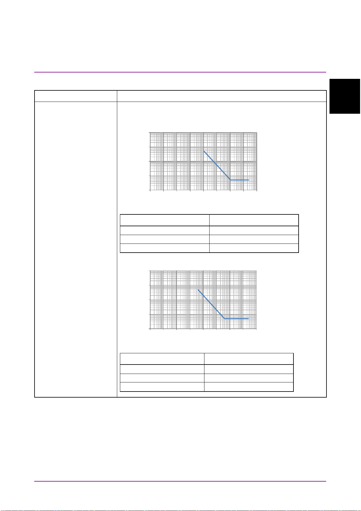
Overview
Table 1.3.2-12 Clock Recovery (Cont’d)
Jitter Tolerance
SSC with 5300 ppm amplitude can be simultaneously applied by using
108,805
5
10,880,528
0.05
250,000,000
0.05
At the bit rate of 25.78125 Gbit/s
40,000
5
4,000,000
0.05
250,000,000
0.05
Jitter Amplitude [UI]
Jitter Amplitude [UI]
1.3 Specifications
Item Specifications
Data Clock Recovery
MU181500B.
At the bit rate of 28.05 Gbit/s
100
10
1
0.1
0.01
10 100 1k 1 0k 100k 1M 10M 100M 100 0M
Modulation Frequency [Hz]
Modulation Frequency (Hz) Jitter Tolerance Mask (UIp-p)
100
1
10
1
0.1
0.01
10 100 1k 10k 100k 1M 10M 100M 1000M
Modulation Frequency [Hz]
Modulation Frequency (Hz) Jitter Tolerance Mask (UIp-p)
1-61
Page 78
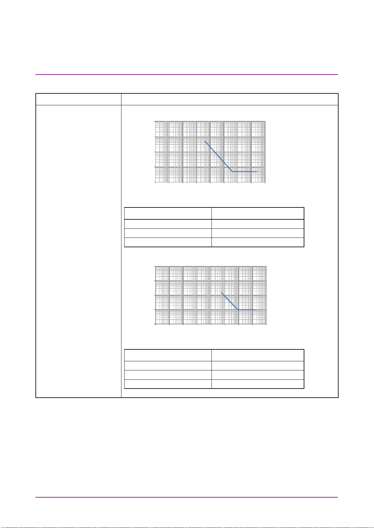
Jitter Tolerance
At the bit rate of 14.0625 Gbit/s
40,000
5
4,000,000
0.05
150,000,000
0.05
At the bit rate of 14.025 Gbit/s
561,000
1.5
8,413,317
0.1
150,000,000
0.1
Jitter Amplitude [UI]
Jitter Amplitude [UI]
Chapter 1 Overview
Item Specifications
Table 1.3.2-12 Clock Recovery (Cont’d)
Data Clock Recovery
(Cont’d)
100
10
1
0.1
0.01
10 1 00 1k 10k 100k 1M 1 0M 100M 1 000M
Modulation Frequency [Hz]
Modulation Frequency (Hz) Jitter Tolerance Mask (UIp-p)
100
10
1
0.1
1-62
0.01
10 100 1k 10k 100k 1M 1 0M 100M 1000M
Modulation Frequency [Hz]
Modulation Frequency (Hz) Jitter Tolerance Mask (UIp-p)
Page 79

Overview
Table 1.3.2-12 Clock Recovery (Cont’d)
Jitter Tolerance
At the bit rate of 10.3125 Gbit/s
40,000
5
4,000,000
0.05
250,000,000
0.05
Jitter Amplitude [UI]
1.3 Specifications
Item Specifications
Clock Recovery (Cont’d)
100
10
1
0.1
0.01
10 100 1k 1 0k 100k 1M 1 0M 100M 1000M
Modulation Frequency [Hz]
Modulation Frequency (Hz) Jitter Tolerance Mask (UIp-p)
1
1-63
Page 80

Jitter tolerance
Bit rate: 16 Gbit/s, 28.1 Gbit/s*, 32.1 Gbit/s*
10
2,000
2,000
7,500
2,000
2,000
100,000
2,000
150
1,000000
200
15
10,000,000
16
1
250,000,000 1 1
When using external
Jitter Amplitude [UI]
Specification
Chapter 1 Overview
Item Specifications
clock
Table 1.3.2-13 Jitter Tolerance
Pattern: PRBS231–1
SSC with a 5300 ppm amplitude and RJ of 0.3 UI can be simultaneously
applied by using MU181500B.
These specifications are defined assuming the following conditions:
Loopback connection to the MU195020A, defined by one specific
temperature in the range of 20 to 30°C.
When RJ+BUJ is bigger than 0.5 UIp-p or SJ + RJ + BUJ is bigger than
the standard value + 0.3 UIp-p, “Overload” is displayed on the
MU181500B screen.
10000
1000
最大印可可能量
MAX. modulation amplitude
規格値
100
10
1
0.1
Modulation
frequency [Hz]
*: When option x01 is installed.
10 100 1k 10k 100k 1M 10M 10 0M 10 00M
Modulation Frequency [Hz]
MAX. modulation
amplitude [UIp-p]
Specification [UIp-
p]
1-64
Page 81

Overview
Table 1.3.2-14 Multichannel operation*1
Combination*2
Number of channels
2
Pattern
At Combination
n = 2 below (2ch combination)
Data Data Length
2 × n to 268435456 × n bits, in n-bit steps*3
Mixed
Row Length
2048 × n to (268435456+231) × n bits, in 1024 × n bit steps*3
Data Length
1024 × n to 268435456 × n bits, in n-bit steps*3
HSSB Data
Not available for combination.
Block Window
Excludes the specified data pattern bit from the measurement target
n = 2 (2ch Combination) is considered in the following:
Setting resolution
Pattern length (bits)
134 217 729 to 268 435 456 × n
Step [bits]
128 × n
Burst
Burst Cycle
25600 × n to 2147483648 × n bits, in 1024 × n bit steps*3
Enable Period
Internal:
12800 × n to 2147482624 × n bits, in 256 × n bit
steps*3
Delay
Internal:
Ext Trigger, Enable:
0 to 2147483640 × n bits, in 8 × n bit steps*
0 to 2147483520 × n bits, in 8 × n bit steps*3
Measurement
Sync Control
Frame length
4 × n to 64 × n bits, in 4 × n bit steps*3
Frame Position
1 to (Pattern Length' – Frame Length + n) bits, in n-bit steps
1.3 Specifications
Item Specifications
according to the settings. (Mask measurement function)
Invalid when “Mixed” is selected for Test Pattern.
Invalid when Zero-substitution is set to “2
2 to 2 097 152 × n
2 097 153 to 4 194 304 × n
4 194 305 to 8 388 608 × n
8 388 609 to 16 777 216 × n
16 777 217 to 33 554 432 × n
33 554 433 to 67 108 864 × n
67 108 865 to 134 217 728 × n
n
–1”.
1
1 × n
2 × n
4 × n
8 × n
16 × n
32 × n
64 × n
Ext Trigger:
*1: Cannot be set when Test Pattern is HSSB Data.
*2: Combination extending over multiple slots cannot be set.
*3: Common to every channel specified by Combination Setting.
steps*
12800 × n to 2147483392× n bits, in 256 × n bit
3
3
1-65
Page 82

Total, Insertion, and Omission
Eye Contour
Measurement target
Data 1 to Data n*4
Eye Margin
Measurement target
Data 1 to Data n*4
Bathtub
Measurement target
Data 1 to Data n*4
Capture
2 Ch Combination is available*3
Dimensions
21 mm (H), 234 mm (W), 175 mm (D), Excluding protrusions
Mass
2.5 kg max.
Operating temperature
15 to 35°C
Storage temperature
–20 to 60°C
PCIe
Supported standards
PCI Express Base Specification Revision 4.0 Version 0.5, 0.7, 1.0
Test target: Root Complex, End Point
Required option
Option x10/x11/x22 or x20/x21/x22
Required software
MX183000A-PL011:
supporting Jitter Tolerance Test.
Chapter 1 Overview
Item Specifications
Error detection mode
Item Specifications
Table 1.3.2-15 Multichannel operation (Cont’d)
*4: Separately specified for each channel.
Table 1.3.2-16 General
Table 1.3.2-17 Extension Function
Item Specifications
PCI Express Base Specification Revision 5.0 Version 1.0
Bitrate: PCIe Gen1, Gen2, Gen3, Gen4, Gen5
Lane number: ×1
This software enables setting DUT to Loopback state
by following PCIe LTSSM and generating a training
sequence required for transition to Loopback state.
MX183000A-PL021:
This software enables setting DUT to Loopback state
by following PCIe LTSSM and supporting negotiation
with DUT. LTSSM state transition can be analyzed as
log. (One MU195020A and one MU195040A are
required for this software.)
MX183000A-PL025:
This software enables extending the functionality of
PL021 to PCIe 5.0.
Adding MX183000A-PL001 to each option of the above software
enables controlling MU195020A, MU181500B, MU195040A and
1-66
Page 83

Overview
Table 1.3.2-17 Extension Function (Cont’d)
Loopback Through
Configuration, Recovery
Test Pattern
Modified Compliance Pattern
PRBS, Data
SKP Ordered Set
Insertion
Enable, Disable
SKP Length/Insertion
For Gen1, Gen2
Interval: 187 to 750, in 1-steps
Dynamic Link Training
Available when using MX183000A-PL021.
Counter
Tx SKP Count,
Error Rate, Error Count (when using MX183000A-PL021)
LTSSM Log
Log Item
LTSSM State, Link Speed, Time[ns]
Log Size
16384 times
Termination condition
Memory full
1.3 Specifications
Item Specifications
Insert Delay Symbol: Enable, Disable (Available for Gen1 and
Gen2)
Insert SRIS: Enable, Disable (Available for Gen3 and
Gen4)
Compliance Pattern
Insert Delay Symbol: Enable, Disable (Available for Gen1 and
Gen2)
User
Length: COM+1, COM+2, COM+3, COM+4, COM+5
Interval: 768 to 3076, in 1-steps
For Gen3, Gen4, Gen5
Length: 8, 12, 16, 20, 24
1
Rx SKP Count (when using MX183000A-PL021)
1-67
Page 84

Operating bit rate
2.4 to 32.1 Gbit/s
Number of channels
2
Number of inputs per
channel
2 (Data, XData) (Differential)
Input amplitude
1.5 Vp-p max. (Single-ended)
3.0 Vp-p max. (Differential)
Offset
–2.0 to 3.3 V
Impedance
50 Ω
Connector
K (f.)
Number of channels
2
Number of outputs per
channel
2 (Data, XData) (Differential)
Insertion loss
–3 dB +1/–2.5 dB*2
Impedance
50 Ω
Connector
K (f.)
Number of channels
1*2
Number of inputs per
channel
2 (Differential)
Input amplitude
1.5 Vp-p max. (Single-ended)
3.0 Vp-p max. (Differential)
Output control
Only Data Input 1 Channel can be turned On and Off.
(Either DMI/CMI or White Noise is selectable.)
Termination
50 Ω, AC coupling
Connector
SMA Connector (f.)
Chapter 1 Overview
1.3.3 Specifications for MU195050A
Table 1.3.3-1 Operating bit rate
Item Specifications
Table 1.3.3-2 Data Input
Item Specifications
Table 1.3.3-3 Data Output*
Item Specifications
*1: The signal that is output from the noise source is AC-coupled.
*2: Defined for 12.890625 GHz and sine wave.
Table 1.3.3-4 External Input*
Item Specifications
1
1
*1: For connecting to G0373A USB3.1 Receiver Test Adapter or the
Gating Output signal of MU195020A.
*2: Data Input 1 Channel only
1-68
Page 85

Overview
Table 1.3.3-5 Differential Mode Interface (DMI)*1
Amplitude
4 to 200 mVp-p (Differential)*2
Amplitude setting step
1 mV
Amplitude accuracy
±20%±10mV*3
Frequency
2 to 10 GHz
Frequency setting step
10 MHz
Waveform
Sine wave
Presets
PCIe 3, PCIe 4, PCIe 5
Output control
Capability of switching ON/OFF of Data Input 1 Channel and Data
(Either Data Input 2 Channel or White Noise can be selected)
Amplitude
10 to 250 mVp-p (Single-ended)*2
Amplitude setting step
2 mV
Amplitude accuracy
±20%±25mV*3
Frequency
Low Band: 100 MHz to 1 GHz
High Band: 1 to 6 GHz
Frequency setting step
Low Band: 1 MHz
High Band: 10 MHz
Waveform
Sine wave
Presets
TBT3, PCIe 4, PCIe 5
Output control
Capability of switching ON/OFF of Data Input 1 Channel and Data
(Either Data Input 2 Channel or White Noise can be selected)
1.3 Specifications
Item Specifications
Input 2 Channel simultaneously.
(Either White Noise or External Input can be selected for Data Input 1
Channel)
*1: The setting is common for Data Input 1 and Data Input 2.
*2: The setting is available from 0 mVp-p. (Accuracy is guaranteed from
4 mVp-p.)
*3: Defined at certain temperature between 20 to 30°C for 2.1 GHz, 4.2
GHz, 10 GHz.
Table 1.3.3-6 Common Mode Interface (CMI)*
1
1
Item Specifications
Input 2 Channel simultaneously.
(Either White Noise or External Input can be selected for Data Input 1
Channel)
*1: The setting is common for Data Input 1 and Data Input 2.
*2: The setting is available from 0 mVp-p. (Accuracy is guaranteed from
10 mVp-p.)
*3: Defined at certain temperature between 20 to 30°C for 120 MHz, 400
MHz, 1 GHz, 6 GHz.
1-69
Page 86

Flatness
±5 dB (10 MHz to 10 GHz)
Crest Factor
> 5 (p-p/rms)
Amplitude
0.2 to 25 mV rms
Amplitude setting step
0.2 mV rms
Amplitude accuracy
±20%±2.5 mV rms*2
ON/ OFF
Capability of switching ON/OFF of Data Input 1 Channel and Data
(Either Channel 2 or DMI/CMI can be selected)
Dimensions
21 mm (H), 234 mm (W), 175 mm (D), Excluding protrusions
Mass
1.2 kg max.
Operating temperature
15 to 35°C
Storage temperature
–20 to 60°C
Chapter 1 Overview
Item Specifications
Table 1.3.3-7 White Noise*1
Input 2 Channel simultaneously.
(Either DMI/CMI or External Input can be selected for Channel 1)
*1: The setting is common for Data Input 1 and Data Input 2.
*2: Defined at one specific temperature between 20 to 30°C, subtracting
the residual noise value from the data by sampling oscilloscope with
50 GHz bandwidth.
Table 1.3.3-8 General
Item Specifications
1-70.
Page 87

Before Use
Before Use Chapter 2
This chapter describes preparations required before using the MP1900A
modules.
2.1
Installation to MP1900A .............................................. 2-2
2.2 How to Operate Application ......................................... 2-2
2.3 Preventing Damage .................................................... 2-2
2
2-1
Page 88

Chapter 2 Before Use
2.1 Installation to MP1900A
For information on how to install the MP1900A modules to the MP1900A
and how to turn on the power, refer to Chapter 3 “Preparation before
Use” in the
MP1900A Signal Quality Analyzer-R Operation Manual
2.2 How to Operate Application
The modules connected to the MP1900A are controlled by operating the
MX190000A Signal Quality Analyzer-R Control Software (hereinafter,
referred to as “MX190000A”).
For information on how to start up, shut down, and operate the
MX190000A, refer to the
Software Operation Manual.
MX190000A Signal Quality Analyzer-R Control
.
2.3 Preventing Damage
Always observe the ratings when connecting to the input and output
connectors of the MP1900A modules.
If an out-of-range signal is input, the MP1900A modules may be
damaged.
2-2
Page 89

2.3 Preventing Damage
Before Use
CAUTION
• When signals are input to the MP1900A modules, avoid
excessive voltage beyond the rating. Otherwise, the
circuit may be damaged.
• When output is used at the 50 Ω GND terminator, never
feed any current or input signals to the output.
• As a countermeasure against static electricity, ground
other devices to be connected (including experimental
circuits) with ground wires before connecting the I/O
connector.
• The outer conductor and core of the coaxial cable may
become charged as a capacitor. Use any metal to
discharge the outer conductor and core before use.
2
• Never open the MP1900A modules. If you open it and
MP1900A modules have failed or sufficient
performance cannot be obtained, we may decline to
repair the MP1900A modules.
• The MP1900A modules have many important circuits
and parts including hybrid ICs. These parts are
extremely sensitive to static electric charges, so never
open the case of the MP1900A modules.
• The hybrid ICs used in the MP1900A modules are
sealed in airtight containers; never open them. If you
open it and the MP1900A modules have failed or
sufficient performance cannot be obtained, we may
decline to repair the MP1900A modules.
To protect the MP1900A modules from electrostatic
•
discharge failure, a conductive sheet should be placed
onto the workbench, and the operator should wear an
electrostatic discharge wrist strap. Always ground the
wrist strap to the workbench antistatic mat or the frame
ground of the MP1900A modules.
2-3
Page 90

Chapter 2 Before Use
CAUTION
There is a risk of damaging connected devices and DUTs
due to a voltage surge that can occur at module output
terminals when powering on / off the MP1900A. Always
follow the precaution below when preparing for
measurement.
• Do not power on / off the MP1900A when the installed
MP1900A modules are connected to other devices or
DUTs.
<Power-on procedure>
1. Make sure the MP1900A modules are not connected to
other devices or DUTs.
2. Power on the MP1900A.
3. Connect the MP1900A modules to other devices and
DUTs.
<Power-off procedure>
1. Make sure the MP1900A modules are not connected to
other devices or DUTs.
2. Power off the MP1900A.
2-4
Page 91

2.3 Preventing Damage
Before Use
CAUTION
When connecting an external device such as a Bias-T to
the output connectors of MP1900A modules, if the output
signal includes any DC voltage, variations in the output of
the DC power supply or load may change the level of the
output signal, risking damage to the internal circuits.
• Do not connect or disconnect any external devices
while DC voltage is impressed.
• Only switch DC power sources ON and OFF when all
equipment connections have been completed.
<Recommended procedure>
Measurement Preparation
1. Connect all equipment.
2. Set the DC power supply output to ON.
3. Set the MP1900A modules output to ON and
complete measurement.
Measurement Preparation
1. Set the equipment output to OFF.
2. Set the DC power supply output to OFF.
3. Disconnect the MP1900A modules, or change the
DUT connections.
Since even unforeseen fluctuations in DC voltage and load
(open or short circuits at the MP1900A modules output
side and changes caused by using a high-frequency probe,
etc.,) can damage the DUT and equipment, we recommend
connecting a 50–ohm resistance in series with the DC
terminal of the Bias-T to prevent risk of damage.
1:
2
2
2-5
Page 92

MU195020A
MP1900A
DUT
DC
50 Ω
Bias-T
Coaxial cable
Coaxial cable
Set output ON/OFF after
To protect DUT and PPG
Do not connect/disconnect while DC
Chapter 2 Before Use
Or
MU195050A
power
source
voltage impressed.
Figure 2.3-1 Bias-T Connection Example
completing connections.
2-6.
Page 93

Panel Layout and Connectors
Panel Layout and Connectors Chapter 3
This chapter describes the panel and connectors of the MP1900A
modules.
3.1
Panel Layout ............................................................... 3-2
3.1.1 MU195020A .................................................... 3-2
3.1.2 MU195040A .................................................... 3-3
3.1.3 MU195050A .................................................... 3-4
3.2 Inter-Module Connection ............................................. 3-5
3.2.1 Measuring Errors............................................. 3-7
3.2.2 Measuring Errors with Noise Added................. 3-9
3.2.3 Adding Jitter to Output Signal ........................ 3-11
3.2.4 Synchronizing Multiple Channels of PPG ....... 3-12
3
3-1
Page 94

[1]
Data Output,
Data
Outputs the differential data signals.
installed option (s).
[2]
Gating Out,
Gating
In case of Repeat: Outputs the timing signals.
[3]
AUX In
Inputs auxiliary signals.
Error Injection, and Burst can be selected.
[4]
AUX Out,
AUX
Outputs auxiliary signals.
connector with the coaxial terminator (J1632A).
[5]
Clock Out
Outputs clock signals.
[6]
Ext Clock In
Inputs clock signals from these units:
External Synthesizer*
[1]
[2]
[3]
[4]
[5]
[6]
[1]
[2]
[3]
[4]
[5]
[6]
Chapter 3 Panel Layout and Connectors
3.1 Panel Layout
3.1.1 MU195020A
Figure 3.1.1-1 Panel layout (MU195020A-x10)
Figure 3.1.1-2 Panel layout (MU195020A-x20)
Table 3.1.1-1 Connectors on panel
No. Name Description
Output
Out
Out
Various interface signals can be output, depending on the
In case of Burst: Outputs the timing signals for Burst.
1/N clock, Pattern Sync, and Burst2 signals can be output
according to the setting.
Because of differential output, be sure to terminate the unused
MU181000A 12.5GHz Synthesizer
MU181000B 12.5GHz 4 Port Synthesizer
MU181500B Jitter Modulation Source
*: We recommend using the MG3690C series as an external
synthesizer.
For details about the MG3690C series, contact Anritsu or our sales
3-2
representative.
Page 95
Panel Layout and Connectors
3.1.2 MU195040A
[1]
Data Input,
Data
Input Data,
Data
data signals.
connector.
[2]
AUX In
Inputs auxiliary signals.
[3]
AUX Out,
AUX
Outputs auxiliary signals. 1/N Clock, Pattern Sync, Error, and
[4]
Ext Clock In
Inputs clock signals.
[1]
[2]
[3]
[4]
[1]
[2]
[3]
[4]
Figure 3.1.2-1 Panel layout (MU195040A-x10)
3.1 Panel Layout
3
Figure 3.1.2-2 Panel layout (MU195040A-x20)
Table 3.1.2-1 Connectors on panel
No. Name Description
Input
Out
Support both differential and single-ended input signals.
When the MU195040A-x22 Clock Recovery is installed, the
clock is recovered from the signal input to the Data Input1
External Mask, Burst, or Capture External Trigger can be
selected.
Sync Gain output signals can be selected.
Because of differential output, be sure to connect the coaxial
terminator (J1632A) to unused side connector.
3-3
Page 96

[1]
Data Output,
Data
Output
Connectors to output differential Data and
Data
signals to
which noise is added.
[2]
Data Input,
Data
Connectors to input Data and
Data
signals to add noise.
Support both differential and single-ended input signals.
[3]
External Input,
External
Inputs auxiliary signals.
MU195020A Gating Output signal.
[1]
[2]
[3]
[2]
[1]
Chapter 3 Panel Layout and Connectors
3.1.3 MU195050A
Figure 3.1.3-1 Panel layout (MU195050A)
Table 3.1.3-1 Connectors on panel
No. Name Description
Input
Input
They are used in connection with BSG4G USB Test Adapter or
3-4
Page 97

Panel Layout and Connectors
3.2 Inter-Module Connection
Avoid static electricity when handling the devices.
• When signals are input to this MP1900A modules, avoid
excessive voltage beyond the rating. Otherwise, the
circuit may be damaged.
3.2 Inter-Module Connection
WARNING
• As a countermeasure against static electricity, ground
other devices to be connected (including experimental
circuits) with ground wires before connecting the I/O
connector.
• The outer conductor and core of the coaxial cable may
become charged as a capacitor. Use any metal to
discharge the outer conductor and core before use.
• The power supply voltage rating for the MP1900A is
shown on the rear panel. Be sure to operate the
MP1900A within the rated voltage range. The MP1900A
may be damaged if a voltage out of the rating range is
applied.
• To protect the MP1900A modules from electrostatic
discharge failure, a conductive sheet should be placed
onto the workbench, and the operator should wear an
electrostatic discharge wrist strap. Always ground the
wrist strap to the workbench antistatic mat or the frame
ground of the MP1900A.
3
When removing a cable from a connector on the front
•
panel of the MP1900A modules, be careful not to add
excessive stress to the connector.
Addition of excessive stress to a connector may result
in characteristic degradation or a failure. Use a torque
wrench (recommended torque: 0.9 N-M) when attaching
or removing a cable.
3-5
Page 98

Chapter 3 Panel Layout and Connectors
Note that the maximum output level of the Data Output
connector of MU195020A-x10/x20 is “1.30 Vp-p” (1.50 Vp-p
when Option x11/x21 is installed). Also, the data output
level of MU195050A is decided by the data input level, and
it is at maximum 1.50 Vp-p. The maximum data input level
of MU195040A is 1.00 V.
When connecting the Data Output connector of
MU195020A/MU195050A directly to the Data Input
connector of MU195040A to verify operation, make sure
that the data output level of MU195020A/MU195050A is 1 V
or under.
Avoid inputting the signal exceeding the maximum input
level to the Data Input connector of MU195040A. Failure to
do so can cause damage.
CAUTION
3-6
Page 99

Panel Layout and Connectors
3.2.1 Measuring Errors
Data
Data
Data
Data
MU195040A
MU195020A
MU181000A
DUT
6 dB ATT
This section describes a connection example of MU195020A, MU181000A
12.5GHz synthesizer (hereafter MU181000A), and MU195040A that are
installed to an MP1900A.
3.2 Inter-Module Connection
3
Figure 3.2.1-1 Inter-module connection example
1. For the case of the MU181000A, attach the 6 dB fixed attenuator
(ATT) to the Clock Output connector.
The following module and options do not require the 6 dB fixed
attenuator.
MU181000A-x01, MU181000B, MU181000B-x01
2. Connect the Clock Output connector of the MU181000A and the Ext.
Clock Input connector of the MU195020A, using a coaxial cable.
3. Connect the Clock Output connector of the MU195020A and the Ext.
Clock Input connector of the MU195040A, using a coaxial cable.
4. Connect the Data Output connector of the MU195020A and the Data
Input connector of the device under test (DUT) using a coaxial cable.
Also connect the
the
5. Connect the Data Output connector of the DUT and the Data Input
connector of the MU195040A, using a coaxial cable. Also connect the
of the MU195040A, using a coaxial cable.
Input connector of the DUT, using a coaxial cable.
Output connector of the DUT and the
Output connector of the MU195020A and
Input connector
3-7
Page 100

Chapter 3 Panel Layout and Connectors
6. Start MX190000A and select Initialize from the Menu to initialize
the entire system.
Note that all the settings are initialized to the factory default
settings by initialization. If necessary, select
save the settings before initialization.
Save from the Menu to
3-8
 Loading...