True Accuracy, 16-Bit ±12 V/±15 V,
FEATURES
Full 16-bit performance
1 LSB max INL and DNL
Output voltage range up to ±14 V
On-board reference buffers, eliminating the need for a
negative reference
Controlled output during power-on
Temperature range of −40°C to +85°C/−40°C to +125°C
Settling time of 10 µs to 0.003%
Clear function to 0 V
LDAC
Asynchronous update of outputs (
Power-on reset
Serial data output for daisy chaining
Data readback facility
APPLICATIONS
Industrial automation
Automatic test equipment
Process control
Data acquisition systems
General-purpose instrumentation
GENERAL DESCRIPTION
The AD5570 is a single 16-bit serial input, voltage output DAC
that operates from supply voltages of ±12 V up to ±15 V.
Integral linearity (INL) and differential nonlinearity (DNL) are
accurate to 1 LSB. During power-up (when the supply voltages
are changing), V
The AD5570 DAC comes complete with a set of reference
buffers. The reference buffers allow a single, positive reference
to be used. The voltage on REFIN is gained up and inverted
internally to give the positive and negative reference for the
DAC core. Having the reference buffers on-chip eliminates the
need for external components such as inverters, precision
amplifiers, and resistors, thereby reducing the overall solution
size and cost.
is clamped to 0 V via a low impedance path.
OUT
pin)
Serial Input Voltage Output DAC
AD5570
FUNCTIONAL BLOCK DIAGRAM
DGND
V
V
DD
SS
AD5570
REFGND
R
R
R
R
REFIN
LDAC
SDIN
16-BIT
DAC
DAC REGISTER
SHIFT REGISTER
SCLK
SYNC
Figure 1.
SDO
purposes. Data readback allows the user to read the contents of
the DAC register via the SDO pin.
LDAC
Features on the AD5570 include
, which may be used to
update the output of the DAC. The device also has a powerdown pin (
power state, and a
PD
), which allows the DAC to be put into a low
CLR
pin that allows the output to be cleared
to 0 V.
The AD5570 is available in a 16-lead SSOP package.
PRODUCT HIGHLIGHTS
1. 1 LSB maximum INL and DNL.
2. Buffered voltage output up to ±14 V.
POWER-ON
RESET
POWER-DOWN
CONTROL LOGIC
CLR
V
OUT
AGND
AGNDS
PD
03760-0-001
The AD5570 uses a versatile 3-wire interface that is compatible
with SPI®, QSPI™, MICROWIRE™, and DSP® interface standards.
Data is presented to the part in the format of a 16-bit serial
word. Serial data is available on the SDO pin for daisy-chaining
Rev. 0
Information furnished by Analog Devices is believed to be accurate and reliable.
However, no responsibility is assumed by Analog Devices for its use, nor for any
infringements of patents or other rights of third parties that may result from its use.
Specifications subject to change without notice. No license is granted by implication
or otherwise under any patent or patent rights of Analog Devices. Trademarks and
registered trademarks are the property of their respective owners.
3. Output controlled during power-up.
4. On-board reference buffers.
5. Wide temperature range of −40°C to +125°C.
One Technology Way, P.O. Box 9106, Norwood, MA 02062-9106, U.S.A.
Tel: 781.329.4700
Fax: 781.326.8703 © 2003 Analog Devices, Inc. All rights reserved.
www.analog.com

AD5570
TABLE OF CONTENTS
Specifications..................................................................................... 3
CLEAR (
CLR
)............................................................................. 17
Standalone Timing Characteristics ................................................ 4
Daisy Chaining and Readback Timing Characteristics............... 6
Absolute Maximum Ratings............................................................ 8
ESD Caution.................................................................................. 8
Pin Configuration and Function Descriptions............................. 9
Te r m in o l o g y .................................................................................... 10
Typical Performance Characteristics ........................................... 11
General Description....................................................................... 16
DAC Architecture .......................................................................16
Reference Buffers........................................................................ 16
Serial Interface............................................................................ 16
Transfe r Fu ncti o n ....................................................................... 17
REVISION HISTORY
Revision 0: Initial Version
Power-Down (
Power-On Reset .......................................................................... 17
Serial Data Output (SDO)......................................................... 17
Applications Information.............................................................. 19
Typical O p e rating Circ u i t ......................................................... 19
Layout Guidelines....................................................................... 20
Opto-Coupler Interface ............................................................. 20
Microprocessor Interfacing....................................................... 20
Evaluation Board ........................................................................ 22
Outline Dimensions....................................................................... 24
Ordering Guide .......................................................................... 24
PD
) ..................................................................... 17
Rev. 0 | Page 2 of 24

AD5570
SPECIFICATIONS
VDD = +11.4 V to +16.5 V; VSS = −11.4 V to −16.5 V; V
specifications T
MIN
to T
, unless otherwise noted.
MAX
Table 1.
A/W Grade
Parameter
Min Typ
3
ACCURACY
Resolution * 16 Bits
Monotonicity * 16 Bits
Relative Accuracy (INL) ±0.6 ±0.4 ±1 LSB At 25°C
±0.6 ±2 −1 ±0.4 +1.25 LSB
Differential Nonlinearity
* * * −1 ±0.3 +1 LSB
(DNL)
Negative Full-Scale Error * * ±0.9 ±7.5 mV
Full-Scale Error * * ±1.8 ± 6 mV
Bipolar Zero Error * * ±0.9 ±7.5 mV
Gain Error * * ±1.8 ±7.5 mV
Gain Temperature
Coefficient
4
* * 0.25 ±1.5
REFERENCE INPUT
Reference Input Range4 * * * 4 5 5 V With ±11.4 V supplies
* * * 4 5 7 V With ±16.5 V supplies
Input Current * ±0.1 µA
OUTPUT CHARACTERISTICS
4
Output Voltage Range * * VSS + 1.4 V VDD − 1.4 V V ±11.4 V supplies
* * VSS + 2.5 V VDD − 2.5 V V ±16.5 V supplies
Output Voltage Settling Time * * 12 16 µs At 16 bits to ±0.5 LSB
* * 10 13 µs To 0.003%
* * 6 7 µs 512 LSB code change
Slew Rate * 6.5 V/µs Measured from 10% to 90%
Digital-to-Analog Glitch
* 15 nV-s
Impulse
Bandwidth * 20 kHz
Short Circuit Current * 25 mA
Output Noise Voltage Density * 85 nV/Hz f = 1 kHz; midscale loaded
DAC Output Impedance
4
* * 0.35 0.5 Ω
Digital Feedthrough * 0.5 nV-s
WARMUP TIME
5
* 12 s
LOGIC INPUTS
Input Current * ±0.1 µA
V
, Input High Voltage * 2 V
INH
V
, Input Low Voltage * 0.8 V
INL
CIN, Input Capacitance
4
* 3 pF
LOGIC OUTPUTS
VOL, Output Low Voltage * 0.4 V I
Floating-State Output
* 8 pF
Capacitance
= 5 V; REFGND = GND = 0 V; RL = 5 kΩ and CL = 200 pF to GND; all
REF
1, 2
Max Min Typ
B/Y Grade
2
3
Max
Unit Test Conditions/Comments
ppm
FSR/°C
±12 V supplies; 1 LSB change
around the major carry
= 1 mA
SINK
Rev. 0 | Page 3 of 24

AD5570
Parameter
A/W Grade
Min Typ
3
1, 2
B/Y Grade
Max Min Typ
2
3
Max
Unit Test Conditions/Comments
POWER REQUIREMENTS
VDD/V
I
DD
I
SS
SS
* * ±11.4 ±16.5 V
* 4 5 mA V
* 3.5 5 mA V
Power-Down Current * 16 µA V
Power Supply Sensitivity
Power Dissipation * 100 mW V
1
Asterisk (*) = specifications same as B/Y grade.
2
Temperature range: A and B = −40°C to +85°C; W and Y = –40°C to +125°C.
3
Typical specifications at ±12 V/±15 V, 25°C.
4
Guaranteed by design.
5
Warmup time is required for the device to reach thermal equilibrium, thus achieving rated performance.
6
Sensitivity of negative full-scale error and positive full-scale error to VDD, VSS variations.
6
* 0.1 LSB/V
unloaded
OUT
unloaded
OUT
unloaded
OUT
±15 V supplies ±10%;
full scale loaded
unloaded
OUT
Rev. 0 | Page 4 of 24

AD5570
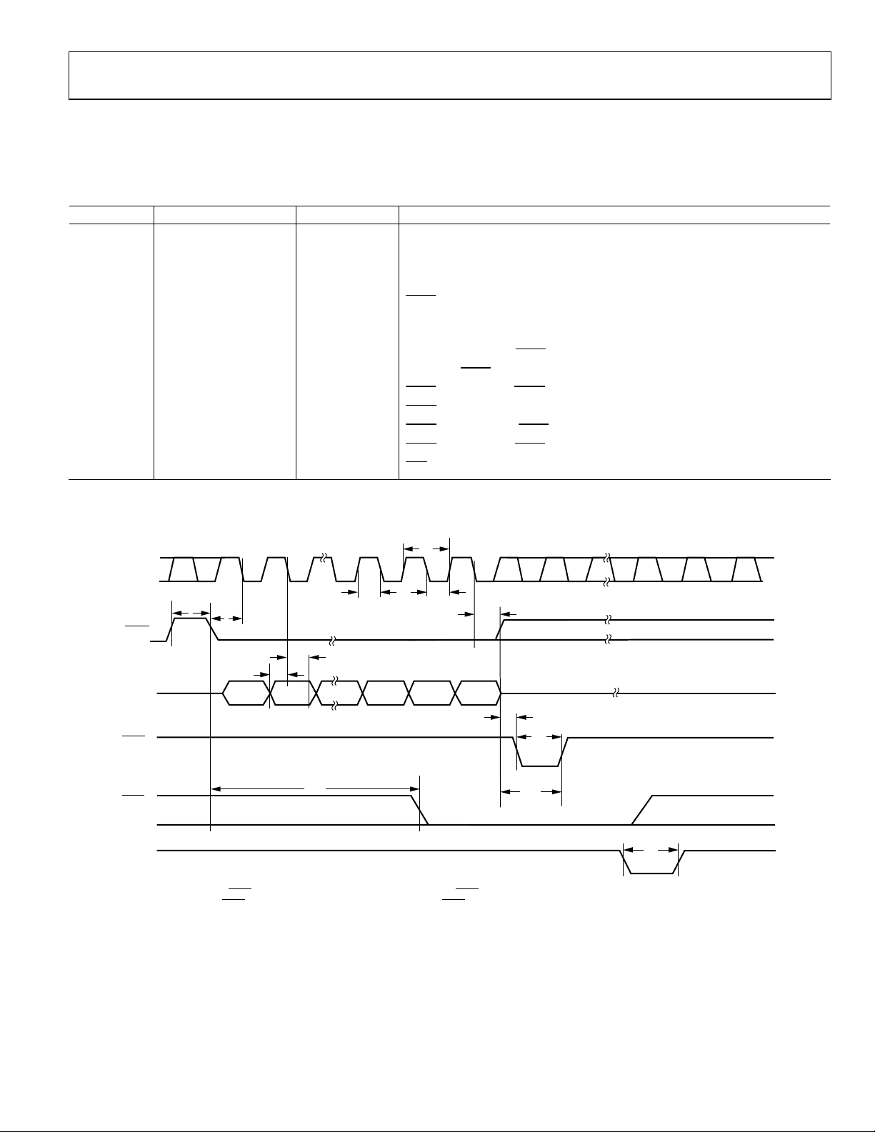
STANDALONE TIMING CHARACTERISTICS
VDD = +12 V ± 5%, VSS = −12 V ± 5% or VDD = +15 V ± 10%, VSS = −15 V ± 10%; V
= 200 pF to GND; all specifications T
and C
L
MIN
to T
, unless other wise noted.
MAX
Table 2.
Parameter Limit at T
f
10 MHz max SCLK frequency
MAX
t
1
t
2
t
3
t
4
t
5
t
6
t
7
t
8
t
9
t
10
t
11
t
12
t
13
All parameters guaranteed by design and characterization. Not production tested.
All input signals are measured with tr = tf = 5 ns (10% to 90% of VDD) and timed from a voltage level of (VIL +VIH)/2.
100 ns min SCLK cycle time
35 ns min SCLK high time
35 ns min SCLK low time
10 ns min
35 ns min Data setup time
0 ns min Data hold time
45 ns min
45 ns min
0 ns min
50 ns min
0 ns min
0 ns min
20 ns min
MIN
, T
Unit Description
MAX
SYNC to SCLK falling edge setup time
SCLK falling edge to
Minimum
SYNC rising edge to LDAC falling edge
LDAC pulse width
LDAC falling edge to SYNC falling edge (no update)
LDAC rising edge to SYNC rising edge (no update)
CLR pulse width
SYNC high time
= 5 V; REFGND = GND = 0 V; RL = 5 kΩ;
REF
SYNC rising edge
t
1
SCLK
t
t
8
t
4
SYNC
t
6
t
5
SDIN
1
LDAC
2
LDAC
CLR
NOTES
1. ASYNCHRONOUS LDAC UPDATE MODE. UPDATE ON FALLING EDGE OF LDAC.
2. SYNCHRONOUS LDAC UPDATE MODE. UPDATE ON RISING EDGE OF SYNC.
DB15
t
11
2
t
3
t
7
DB0
t
9
t
10
t
12
t
13
03760-0-002
Figure 2. Serial Interface Timing Diagram
Rev. 0 | Page 5 of 24

AD5570
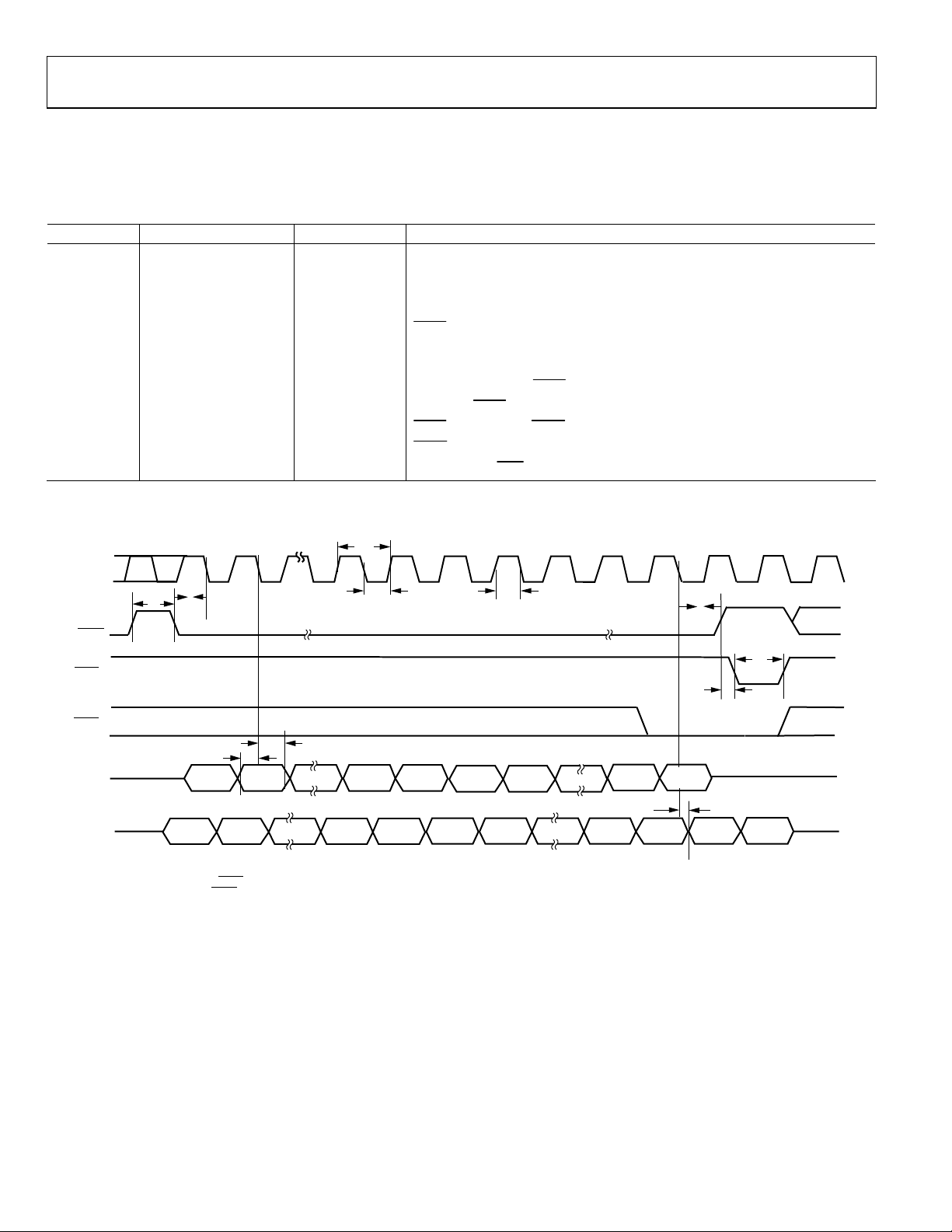
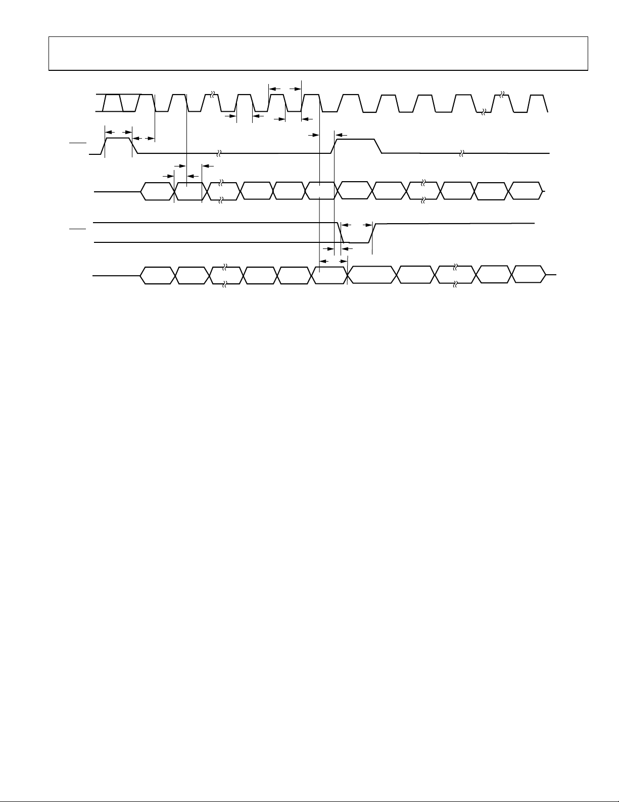
DAISY-CHAINING AND READBACK TIMING CHARACTERISTICS
V
= +12 V ± 5%, VSS = −12 V ± 5% or VDD = +15 V ± 10%, VSS = −15 V ± 10%; V
DD
= 200 pF to GND; all specifications T
and C
L
MIN
to T
, unless other wise noted.
MAX
Table 3.
Parameter Limit at T
f
MAX
t
1
t
2
t
3
t
4
t
5
t
6
t
7
t
8
t
9
t
10
1
t
14
All parameters guaranteed by design and characterization. Not production tested.
All input signals are measured with tr = tf = 5 ns (10% to 90% of V
SDO; R
PULLUP
1
With CL = 0 pF, t15 = 100 ns.
SCLK
2 MHz max SCLK frequency
500 ns min SCLK cycle time
200 ns min SCLK high time
200 ns min SCLK low time
10 ns min
35 ns min Data setup time
0 ns min Data hold time
45 ns min
45 ns min
0 ns min
50 ns min
200 ns max
= 5 kΩ, CL = 15 pF.
t
8
, T
MIN
Unit Description
MAX
SYNC to SCLK falling edge setup time
SCLK falling edge to
Minimum
SYNC high time
SYNC rising edge to LDAC falling edge
LDAC pulse width
Data delay on
) and timed from a voltage level of (VIL +VIH)/2.
DD
t
1
t
4
t
3
SDO
t
= 5 V; REFGND = GND = 0 V; RL = 5 kΩ,
REF
SYNC rising edge
2
t
7
SYNC
t
LDAC
LDAC
SDIN
SDO
1
2
t
5
DB15 (N)
NOTES
1. ASYNCHRONOUS LDAC UPDATE MODE
2. SYNCHRONOUS LDAC UPDATE MODE
t
6
DB0 (N)
DB0
(N+1)
DB15
(N+1)
DB0 (N)
DB15 (N)
DB15
(N+1)
10
t
9
t
14
03760-0-003
Figure 3. Daisy-Chaining Timing Diagram
Rev. 0 | Page 6 of 24

AD5570
t
1
SCLK
t
2
t
8
t
4
SYNC
t
6
t
5
SDIN
LDAC
SDO
DB15 (N) DB0 (N)
t
3
t
7
DB15
(N+1)
t
10
t
9
t
14
Figure 4. Readback Timing Diagram
DB0
(N+1)
DB0 (N)DB14 (N)DB15 (N)
03760-0-004
Rev. 0 | Page 7 of 24

AD5570
ABSOLUTE MAXIMUM RATINGS
TA = 25°C, unless otherwise noted.
Table 4.
Parameter Rating
VDD to AGND, AGNDS, DGND −0.3 V, +17 V
VSS to AGND, AGNDS, DGND +0.3 V, −17 V
AGND, AGNDS to DGND −0.3 V to +0.3 V
REFGND to AGND, ADNDS VSS − 0.3 V to VDD + 0.3 V
REFIN to AGND, AGNDS VSS − 0.3 V to VDD + 0.3 V
REFIN to REFGND −0.3 V to +17 V
Digital Inputs to DGND −0.3 V to VDD + 0.3 V
V
to AGND, AGNDS −0.3 V to VDD + 0.3 V
OUT
SDO to DGND −0.3 V to +6.5 V
Operating Temperature Range: −40°C to +125°C
W, Y Grades −40°C to +125°C
A, B Grades −40°C to +85°C
Storage Temperature Range −65°C to +150°C
Maximum Junction Temperature
(TJ Max) 150°C
16-Lead SSOP Package
Power Dissipation (TJ max – TA)/θ
θJA Thermal Impedance 139°C/W
Lead Temperature (Soldering 10 s) 300°C
IR Reflow, Peak Temperature 230°C
JA
Stresses above those listed under Absolute Maximum Ratings
may cause permanent damage to the device. This is a stress
rating only and functional operation of the device at these or
any other conditions above those listed in the operational
sections of this specification is not implied. Exposure to
absolute maximum rating conditions for extended periods may
affect device reliability.
ESD CAUTION
ESD (electrostatic discharge) sensitive device. Electrostatic charges as high as 4000 V readily accumulate on
the human body and test equipment and can discharge without detection. Although this product features
proprietary ESD protection circuitry, permanent damage may occur on devices subjected to high energy
electrostatic discharges. Therefore, proper ESD precautions are recommended to avoid performance
degradation or loss of functionality.
Rev. 0 | Page 8 of 24
 Loading...