

DACPORT, Low-Cost Complete
a
FEATURES
Complete 8-Bit DAC
Voltage Output—0 V to 2.56 V
Internal Precision Band-Gap Reference
Single-Supply Operation: +5 V (610%)
Full Microprocessor Interface
Fast: 1 ms Voltage Settling to 61/2 LSB
Low Power: 75 mW
No User Trims Required
Guaranteed Monotonic Over Temperature
All Errors Specified T
Small 16-Pin DIP or 20-Pin PLCC Package
Low Cost
GENERAL DESCRIPTION
The AD557 DACPORT® is a complete voltage-output 8-bit
digital-to-analog converter, including output amplifier, full
microprocessor interface and precision voltage reference on a
single monolithic chip. No external components or trims are
required to interface, with full accuracy, an 8-bit data bus to an
analog system.
The low cost and versatility of the AD557 DACPORT are the result of continued development in monolithic bipolar technologies.
The complete microprocessor interface and control logic is
implemented with integrated injection logic (I
dense and low-power logic structure that is process-compatible
with linear bipolar fabrication. The internal precision voltage
reference is the patented low-voltage band-gap circuit which
permits full-accuracy performance on a single +5 V power supply. Thin-film silicon-chromium resistors provide the stability
required for guaranteed monotonic operation over the entire
operating temperature range, while laser-wafer trimming of
these thin-film resistors permits absolute calibration at the factory to within ±2.5 LSB; thus, no user-trims for gain or offset
are required. A new circuit design provides voltage settling to
±1/2 LSB for a full-scale step in 800 ns.
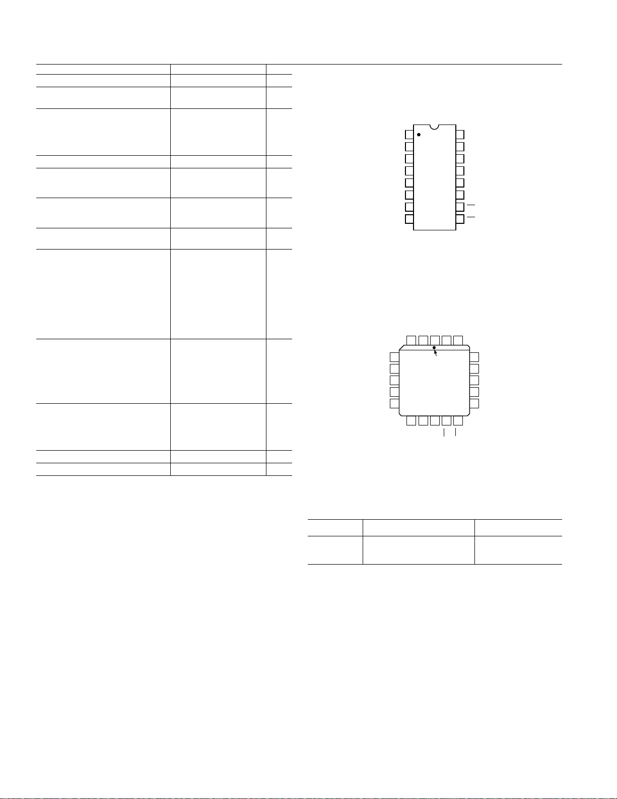
The AD557 is available in two package configurations. The
AD557JN is packaged in a 16-pin plastic, 0.3"-wide DIP. For
surface mount applications, the AD557JP is packaged in a
20-pin JEDEC standard PLCC. Both versions are specified over
the operating temperature range of 0°C to +70°C.
MIN
to T
MAX
2
L), an extremely
mP-Compatible 8-Bit DAC
AD557
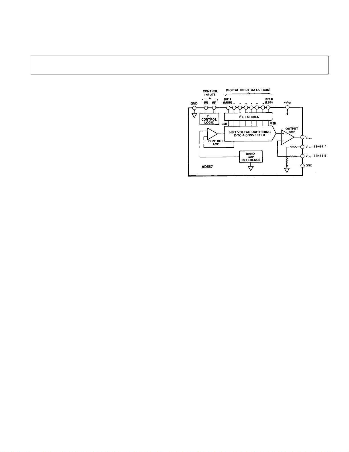
FUNCTIONAL BLOCK DIAGRAM
PRODUCT HIGHLIGHTS
1. The 8-bit I2L input register and fully microprocessorcompatible control logic allow the AD557 to be directly connected to 8- or 16-bit data buses and operated with standard
control signals. The latch may be disabled for direct DAC
interfacing.
2. The laser-trimmed on-chip SiCr thin-film resistors are calibrated for absolute accuracy and linearity at the factory.
Therefore, no user trims are necessary for full rated accuracy
over the operating temperature range.
3. The inclusion of a precision low-voltage band-gap reference
eliminates the need to specify and apply a separate reference
source.
4. The AD557 is designed and specified to operate from a single
+4.5 V to +5.5 V power supply.
5. Low digital input currents, 100 µA max, minimize bus loading.
Input thresholds are TTL/low voltage CMOS compatible.
6. The single-chip, low power I
ently more reliable than hybrid multichip or conventional
single-chip bipolar designs.
2
L design of the AD557 is inher-
DACPORT is a registered trademark of Analog Devices, Inc.
Covered by U.S. Patent Nos. 3,887,863; 3,685,045; 4,323,795; other
patents pending.
REV. A
Information furnished by Analog Devices is believed to be accurate and
reliable. However, no responsibility is assumed by Analog Devices for its
use, nor for any infringements of patents or other rights of third parties
which may result from its use. No license is granted by implication or
otherwise under any patent or patent rights of Analog Devices.
One Technology Way, P.O. Box 9106, Norwood, MA 02062-9106, U.S.A.
Tel: 617/329-4700 Fax: 617/326-8703
AD557–SPECIFICATIONS
10
9
13
12
11
16
15
14
8
1
2
3
4
7
6
5
TOP VIEW
(Not to Scale)
AD557
LSB BIT 8
GND
V
OUT
SENSE B
V
OUT
SENSE A
V
OUT
BIT 7
BIT 6
BIT 5
CS
+V
CC
GNDBIT 4
BIT 3
BIT 2
MSB BIT 1
CE
NC
20 19
18
123
4
5
6
7
8
9101112
13
14
15
16
17
TOP VIEW
(Not to Scale)
PIN 1
IDENTIFIER
BIT 6
BIT 5
NC
BIT 4
BIT 3
V
OUT
SENSE B
GND
NC
GND
+V
CC
NC = NO CONNECT
AD557
BIT 7
BIT 8 (LSB)
NC
V
OUT
V
OUT
SENSE A
BIT 2
(MSB) BIT 1
CE
CS
(@ TA = +258C, VCC = +5 V unless otherwise noted)
Model Min Typ Max Units
RESOLUTION 8 Bits
RELATIVE ACCURACY
0 to + 70°C ±1/2 1 LSB
OUTPUT
Ranges 0 to + 2.56 V
Current Source +5 mA
Sink Internal Passive
Pull-Down to Ground
OUTPUT SETTLING TIME
FULL-SCALE ACCURACY
3
4
0.8 1.5 µs
@ +25°C ±1.5 ± 2.5 LSB
T
MIN
to T
MAX
±2.5 ±4.0 LSB
ZERO ERROR
@ +25°C ±1 LSB
T
to T
MIN
MAX
MONOTONICITY
T
to T
MIN
MAX
5
±3 LSB
Guaranteed
DIGITAL INPUTS
T
to T
MIN
Input Current 6100 µA
MAX
Data Inputs, Voltage
Bit On—Logic “1” 2.0 V
Bit On—Logic “0” 0 0.8 V
Control Inputs, Voltage
On—Logic “1” 2.0 V
On—Logic “0” 0 0.8 V
Input Capacitance 4 pF
6
TIMING
tW Strobe Pulse Width 225 ns
T
to T
MIN
MIN
MIN
to T
to T
MAX
MAX
MAX
tDH Data Hold Time 10 ns
T
tDS Data Setup Time 225 ns
T
300 ns
10 ns
300 ns
POWER SUPPLY
Operating Voltage Range (VCC)
2.56 Volt Range +4.5 +5.5 V
Current (ICC)1525 mA
Rejection Ratio 0.03 %/%
POWER DISSIPATION, VCC = 5 V 75 125 mW
OPERATING TEMPERATURE RANGE 0 +70 °C
NOTES
1
Relative Accuracy is defined as the deviation of the code transition points from the
ideal transfer point on a straight line from the zero the the full scale of the device.
2
Passive pull-down resistance is 2 kΩ.
3
Settling time is specified for a positive-going full-scale step to ±1/2 LSB. Negativegoing steps to zero are slower, but can be improved with an external pull-down.
4
The full-scale output voltage is 2.55 V and is guaranteed with a +5 V supply.
5
A monotonic converter has a maximum differential lineraity error of ±1 LSB.
6
See Figure 7.
Specifications subject to change without notice.
ABSOLUTE MAXIMUM RATINGS
*
VCC to Ground . . . . . . . . . . . . . . . . . . . . . . . . . . . 0 V to +18 V
Digital Inputs (Pins 1–10) . . . . . . . . . . . . . . . . . .0 V to +7.0 V
V
. . . . . . . . . . . . . . . . . . . . . . . Indefinite Short to Ground
OUT
Momentary Short to V
Power Dissipation . . . . . . . . . . . . . . . . . . . . . . . . . . . .450 mW
Storage Temperature Range
N/P (Plastic) Packages . . . . . . . . . . . . . . . .–25°C to +100°C
Lead Temperature (Soldering, 10 sec) . . . . . . . . . . . . . . 300°C
Thermal Resistance
Junction to Ambient/Junction to Case
*Stresses above those listed under “Absolute Maximum Ratings” may cause
permanent damage to the device. This is a stress rating only and functional
operation of the device at these or any other conditions above those indicated
in the operational section of this specification is not implied. Exposure to absolute
maximum rating conditions for extended periods may affect device reliability.
N/P (Plastic) Packages . . . . . . . . . . . . . . . . . .140/55°C/W
PIN CONFIGURATIONS
DIP
2
PLCC
ORDERING GUIDE
Model Temperature Range Package Option*
AD557JN 0°C to +70°C N-16
AD557JP 0°C to +70°C P-20A
*N = Plastic DIP; P = Plastic Leaded Chip Carrier.
CIRCUIT DESCRIPTION
The AD557 consists of four major functional blocks fabricated
on a single monolithic chip (see Figure 1). The main D/A converter section uses eight equally weighted laser-trimmed current
CC
sources switched into a silicon-chromium thin-film R/2R resistor
ladder network to give a direct but unbuffered 0 mV to 400 mV
output range. The transistors that form the DAC switches are
PNPs; this allows direct positive-voltage logic interface and a
zero-based output range.
–2–
REV. A
 Loading...