

Yaesu VX-7R Service manual
50/144/430 MHz Triple-Band
Heavy Duty Submersible Transceiver
VX-7R
Technical Supplement
©2003 VERTEX STANDARD CO., LTD. EH009M90B
Introduction
the VX-7R 50/144/430 MHzTriple-Band Heavy Duty Submersible Trans-
ceiver.
chip components. Attempts by non-qualified persons to service this
equipment may result in permanent damage not covered by the war-
ranty, and may be illegal in some countries.
this transceiver. Each side of the board is referred to by the type of the
majority of components installed on that side ("Side A" or "Side B"). In
most cases one side has only chip components, and the other has either
a mixture of both chip and leaded components (trimmers, coils, electro-
DW
lytic capacitors, ICs, etc.), or leaded components only.
TEX STANDARD assumes no liability for damage that may occur as a
result of typographical or other errors that may be present. Your coop-
eration in pointing out any inconsistencies in the technical information
would be appreciated.
VERTEX STANDARD CO., LTD.
4-8-8 Nakameguro, Meguro-Ku, Tokyo 153-8644, Japan
VERTEX STANDARD
US Headquarters
10900 Walker Street, Cypress, CA 90630, U.S.A.
YAESU EUROPE B.V.
P.O. Box 75525, 1118 ZN Schiphol, The Netherlands
YAESU UK LTD.
Unit 12, Sun Valley Business Park, Winnall Close
Winchester, Hampshire, SO23 0LB, U.K.
VERTEX STANDARD HK LTD.
Unit 5, 20/F., Seaview Centre, 139-141 Hoi Bun Road,
Kwun Tong, Kowloon, Hong Kong
This manual provides the technical information necessary for servicing
Servicing this equipment requires expertise in handing surface-mount
Two PCB layout diagrams provided for each double-sided board in
While we believe the information in this manual to be correct, VER-
Contents
Specification ............................................................................................................................................ 2
Exploded View & Miscellaneous Parts .............................................................................................4
Block Diagram ........................................................................................................................................ 5
Interconnection Diagram ...................................................................................................................... 6
Circuit Description................................................................................................................................ 7
Alignment .............................................................................................................................................. 11
Board Unit (Schematics, Layouts & Parts)
RF Unit ............................................................................................................................................................................. 19
AF Unit ............................................................................................................................................................................ 33
CNTL Unit ....................................................................................................................................................................... 45
VCO Unit ......................................................................................................................................................................... 59
1

Specifications
General
Frequency Ranges:
Channel Steps:
Frequency Stability:
Emission Type:
Antenna Impedance:
Supply Voltage:
Current Consumption:
Operating Temperature:
Case Size:
Weight:
Rx (MAIN):
0.5 - 1.8 MHz (BC Band)
1.8 - 30 MHz (SW Band)
30-59 MHz (50 MHz HAM: USA version)
30-76 MHz (50 MHz HAM: EXP version)
59-108 MHz (FM: USA version)
76-108 MHz (FM: EXP version)
108-137 MHz (Air Band)
137-174 MHz (144 MHz HAM)
174-222 MHz (VHF-TV)
222-225 MHz (220 MHz HAM: USA version)
225-420 MHz (ACT1: Action Band 1: USA version)
222-420 MHz (ACT1: Action Band 1: EXP version)
420-470 MHz (430 MHz HAM)
470-729 MHz (UHF-TV: USA version)
470-800 MHz (UHF-TV: EXP version)
800-999 MHz (ACT2: Action Band 2, cellular Blocked)
Rx (SUB):
50 - 54 MHz
137 - 174 MHz
420 - 470 MHz
Tx: 50 - 54 MHz (MAIN & SUB)
144 - 146 MHz or 144 - 148 MHz (MAIN & SUB)
222-225 MHz (MAIN, USA version)
430 - 440 MHz or 430 - 450 MHz (MAIN & SUB)
5/9/10/12.5/15/20/25/50/100 kHz
±5 ppm (+14°F to +122°F, –10°C to +50°C)
F2, F3, A3
50-ohm
Nominal: 7.4 V DC, Negative Ground
Operating: 10 - 16 V DC, Negative Ground (EXT DC jack)
150 mA (Mono Band Receive)
200 mA (Dual Band Receive)
55 mA (Mono Band Receive, Standby, Saver Off)
100 mA (Dual Band Receive, Standby, Saver Off)
25 mA (Mono Band Receive, Standby, Saver On "Save Ratio 1:5")
50 mA (Dual Band Receive, Standby, Saver On "Save Ratio 1:5")
400 µA (Auto Power Off)
1.6/1.3/1.0/0.7 A (50 MHz, Tx HI/L3/L2/L1)
1.71.4/1.1/0.8 A (144 MHz, Tx HI/L3/L2/L1)
0.6 A (220 MHz, Tx)
1.8/1.5/1.2/0.9/ A (430 MHz, Tx HI/L3/L2/L1)
–4°F to +140°F (–20°C to +60°C)
60 (W) x 90 (H) x 28 (D) mm (w/o knob & antenna)
250 g
2

Transmitter
RF Power Output:
Modulation Type:
Maximum Deviation:
Spurious Emission:
Microphone Impedance:
Receiver
Circuit Type:
Intermediate Frequencies:
Sensitivity:
Selectivity:
AF Output:
Specifications
5/2.5/1.0/0.5 W (50/144/430 MHz, FM)
0.3 W (220 MHz, FM)
1.0 W (50 MHz, FM)
FM: Variable Reactance
AM: Early Stage (Low Level)
±5/±2.5 kHz
At least 60 dB below (@ Tx 1W)
2 k-ohm
N-FM, AM: Double-Conversion Superheterodyne
W-FM: Triple-Conversion Superheterodyne
1st: 47.25 MHz (N-FM, AM)
45.8 MHz (W-FM)
2nd: 450 kHz (N-FM, AM)
10.7 MHz (W-FM)
3rd: 1 MHz (W-FM)
3.0 µV for 10 dB SINAD (0.5 - 30 MHz, AM)
0.5 µV for 12 dB SINAD (30 - 50 MHz, N-FM)
0.16 µV for 12 dB SINAD (50 - 54 MHz, N-FM)
15 kHz/35 kHz (-6 dB/-60 dB: N-FM, AM)
200 kHz/300 kHz (-6 dB/-20 dB: W-FM)
200 mW @ 8 ohm for 10 % THD (@ 7.4V DC)
400 mW @ 8 ohm for 10 % THD (@ 13.8V DC)
Specifications are subject to change without notice, and are guaranteed within amateur bands only.
3
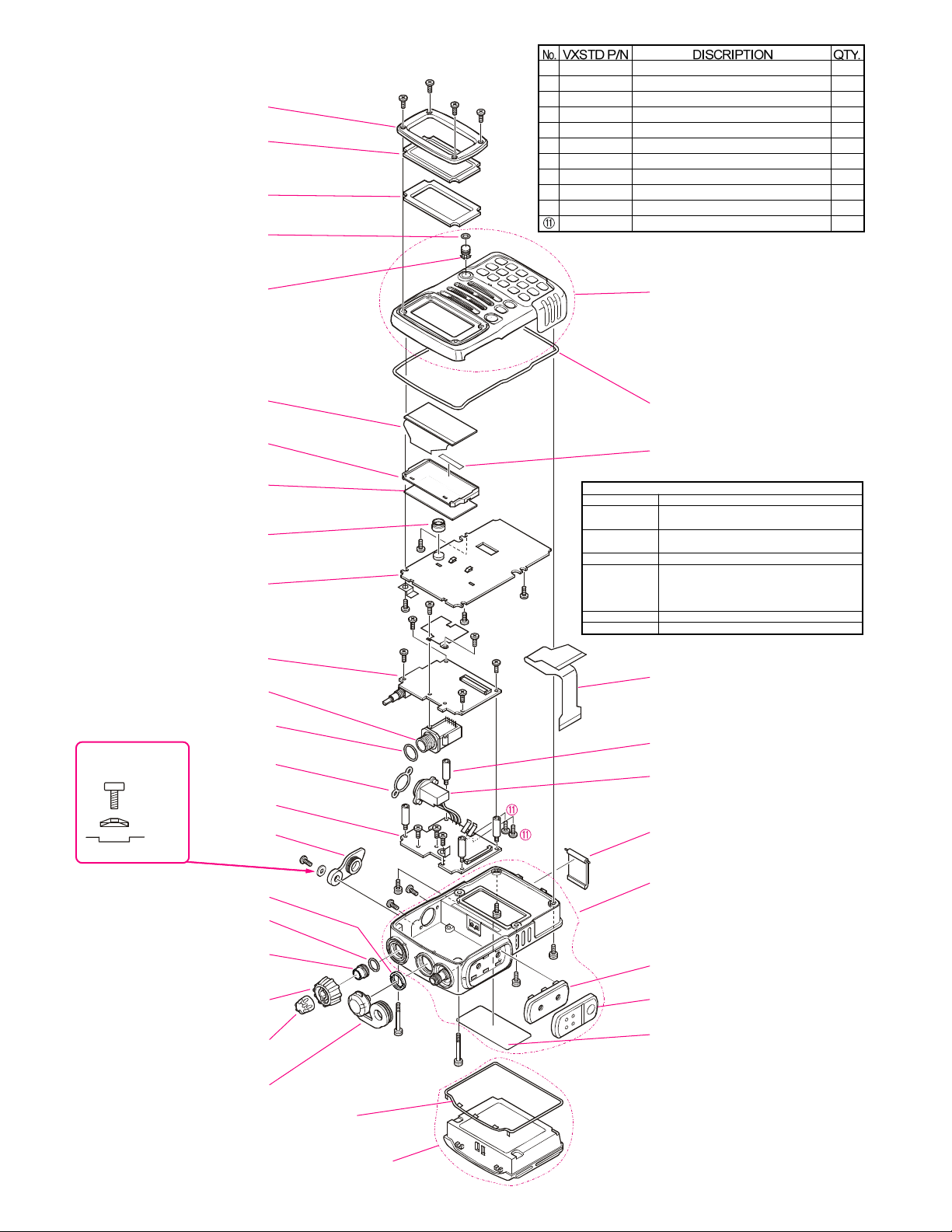
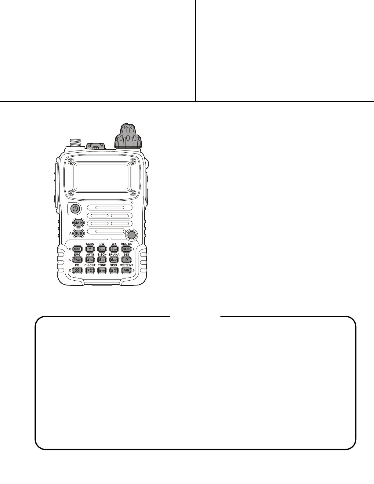
Exploded View & Miscellaneous Parts
RA0417100
PANEL FRAME
RA0399500
WINDOW
RA0399400
DOUBLE FACE TAPE
RA0401600
O RING
RA0399800
LIGHT GUIDE (LED)
Q7000426
LCD MODULE
RA0399100
LIGHT GUIDE (LED)
RA0399900
REFLECTOR SHEET
RA0405600
MIC HOLDER RUBBER
CNTL-Unit
AF-Unit
P1091150
CONNECTOR (MIC/SP)
U9900137
U9900138
U07225120
U9900136
RA0304300
U00103002
U00104002
U9900140
U44104002
U9900141
U07125102
VXSTD P/N DISCRIPTION
Q3000183 YHA-64
Q3000185 YHA-65
Q8101014 YHA-63 50MHZ ADAPTER L
Q8101015 YHA-63 440MHZ ADAPTER S
Q9000786 LI-ION BATTERY FNB-80LI
Q9500087 NC-72A
Q9500088 NC-72B
Q9500089 NC-72C
Q9500090 NC-72U
RA029630A BELT CLIP
S6000335 HAND STRAP
BINDING HEAD SCREW M2X21.7 (W/ O RING)
BINDING HEAD SCREW M2X5 (W/ O RING)
PAN HEAD SCREW M2X2.5SUS#1
SPECIAL SCREW M2X2.35
WASHER
PAN HEAD SCREW M2X3NI
PAN HEAD SCREW M2X4NI
TAPTITE SCREW M2X6SUS#3
TAPTITE SCREW M2X4NI
TAPTITE SCREW M1.7X5NI#3
TAPTITE SCREW M1.7X2.5SUS#1
CP7346002 (USA, SILVER)
CP7346003 (EXPORT, SILVER)
CP7346004 (GERMANY, SILVER)
CP7346006 (USA, BLACK)
CP7346007 (EXPORT, BLACK)
CP7346008 (GERMANY, BLACK)
PANEL ASS’Y
with RUBBER KNOB, MIC SHEET,
SP SHEET, SP, PROTECTOR L,
PROTECTOR R
RA0400000
RUBBER PACKING
RA014250A
DOUBLE FACE TAPE (LCD)
SUPPLIED ACCESSORIES
(depending on transceiver version)
(depending on transceiver version)
FR008330C
FPC CABLE
2
4
4
1
1
1
6
2
4
2
2
There is a direction in
WASHER.
SCREW
WASHER
EXP CAP
RA0401200
ENCODER KNOB
RA0426800
O RING
RA0400900
O RING
RF-Unit
RA0400500
EXT CAP
RA0292200
SPECIAL NUT
RA0426900
O RING
RA0087900
SPECIAL NUT
RA0401900
VOLUME KNOB
RA0400600
CAP(SP/MIC)
RA0141600
RUBBER PACKING
FNB-80LI
RA0400200
STUD (X4 pcs)
P0091335
CONNECTOR (EXT DC)
RA01403AA
LATCH NAIL
CP7342003 (SILVER)
CP7342005 (BLACK)
REAR CASE ASS’Y
with SMA CONNECTOR ASS’Y,
TERMINAL BOARD ASS’Y,
RUBBER HOLDER (PTT),
RUBBER KNOB (PTT)
RA0399700
HOLDER (PTT)
RA0400100
RUBBER KNOB (PTT)
RA0140100
MASK SHEET
4
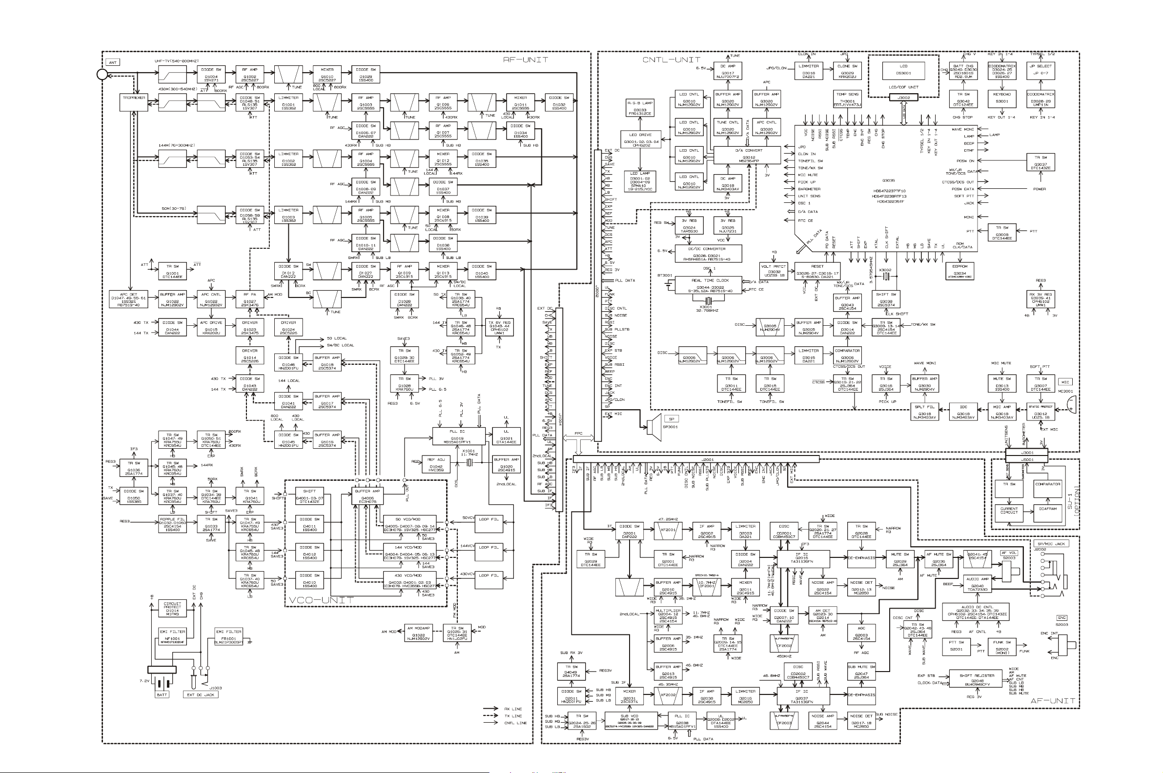
Block Diagram
5
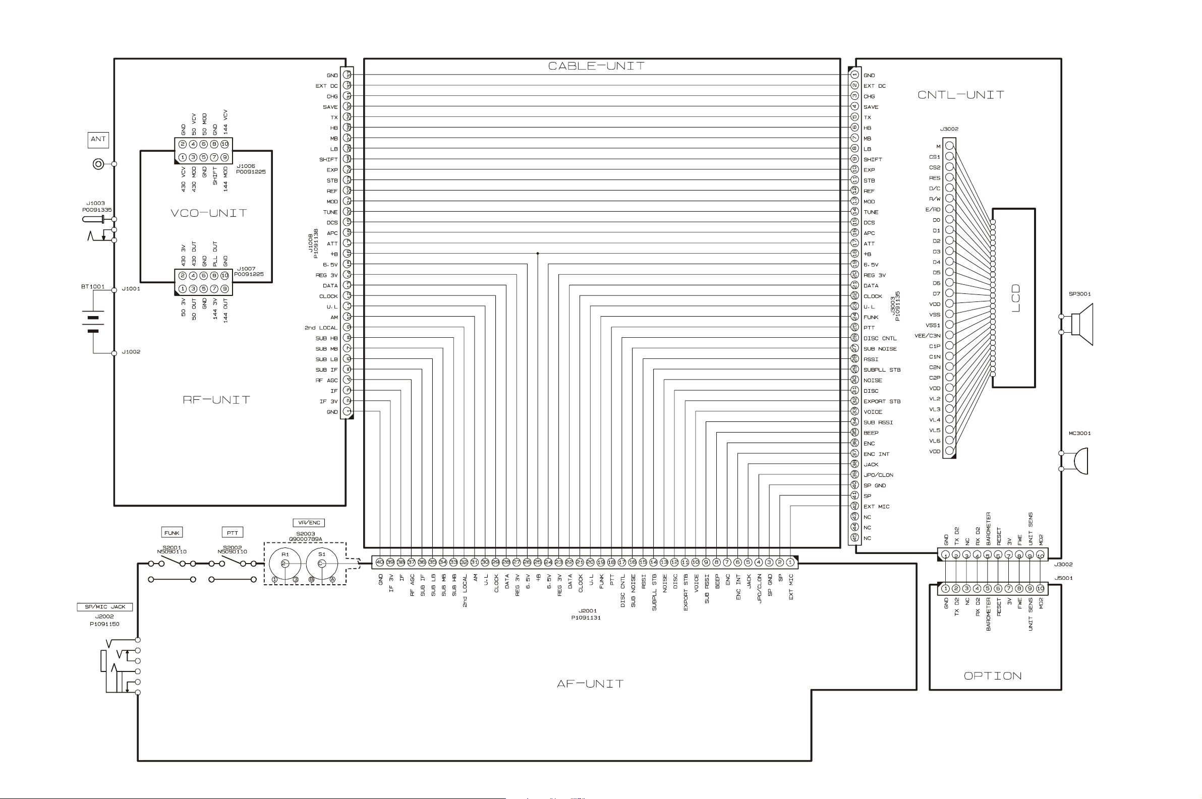
Interconnection Diagram
6

Circuit Description
The VX-7R consists of a RF-UNIT, a CNTL-UNIT and
an AF-UNIT. The RF-UNIT contains the receiver front end,
PLL IC, power and switching circuits, and the VCO-UNIT
for transmit and receive local signal oscillation. The CNTL-
UNIT contains the CPU, and audio ICs, and the power
circuitry for the LCD. The AF-UNIT contains the IF, and
audio ICs.
Receiver Signal Flow
The VX-7R includes five receiver front ends, each op-
timized for a particular frequency range and mode com-
bination.
(1) Triplexer
Signals between 0.5 and 540 MHz received at the an-
tenna terminal pass through a first low-pass filter com-
posed of C1266, C1269, C1289, C1291, C1296, C1297,
L1059, L1060, L1067 and L1068.
Received 430-MHz signals, after passing through the
low-pass filter, are fed to the UHF T/R switch circuit com-
posed of diode switch D1048 (RLS135), D1051 (1SV307).
Received 145-MHz signals, after passing through the
low-pass filter, are fed to the VHF T/R switch circuit com-
posed of diode switch D1053 (RLS135), D1054 (1SV307).
Received 50-MHz signals, after passing through the low-
pass filter, are fed to the 50MHz T/R switch circuit com-
posed of diode switch D1058 (RLS135), D1059 (1SV307).
(2) 145-MHz Band and 76-300MHz Reception
Received signals between 76 and 300 MHz pass through
the Triplexer circuit, low-pass filter/high-pass filter cir-
cuit, VHF T/R switch circuit and protector diode D1002
(1SS362) before additional filtering by a band-pass filter
prior to application to RF amplifier Q1004 (2SC5555). The
amplified RF signal is passed through a band-pass filter
to first mixer Q1012 (2SC5555). Meanwhile, VHF output
from the VCO-UNIT is amplified by Q1017 (2SC5374)
and applied through diode T/R switch D1041 (DAN222)
to mixer Q1012 as the first local signal.
The 47.25-MHz intermediate frequency product of the
mixer is delivered to the AF-UNIT.
The TUNE voltage from the CPU on the CNTL-UNIT is
amplified by DC amplifier Q3017 (NJU7007F2) and ap-
plied to varactors D1020 and D1022 (HVC369B), D1019,
D1021, D1023, D1024, D1033 and D1036 (1SV325) in the
variable frequency band-pass filters. By changing the elec-
trostatic capacitance of the varactors, optimum filter char-
acteristics are provided for each specific operating fre-
quency.
(3) 435-MHz Band and 222-540MHz Reception
Received signals between 222 and 540 MHz pass
through the Triplexer circuit, low-pass filter/high-pass
filter circuit, UHF T/R switch circuit and protector diode
D1001 (1SS362) before additional filtering by a band-pass
filter prior to application to RF amplifier Q1003
(2SC5555). The amplified RF signal is passed through a
band-pass filter, RF amplifier Q1006 (2SC5555) and band-
pass filter to first mixer Q1011 (2SC5555). Meanwhile,
UHF output from the VCO-UNIT is amplified by Q1016
(2SC5374) and applied through diode T/R switch D1045
(HN2D01FU) to mixer Q1011 as the first local signal.
The 47.25-MHz intermediate frequency product of the
mixer is delivered to the AF-UNIT.
The TUNE voltage from the CPU on the CNTL-UNIT is
amplified by DC amplifier Q3017 and applied to varac-
tors D1005, D1018, D1030 and D1031 (HVC358B) in the
variable frequency band-pass filters. By changing the elec-
trostatic capacitance of the varactors, optimum filter char-
acteristics are provided for each specific operating fre-
quency.
(4) 50-MHz-Band and 30-76 MHz Reception
Received signals between 30 and 76 MHz pass through
the Triplexer circuit, low-pass filter circuit, 50 MHz T/R
switch circuit and protector diode D1003 (1SS362) be-
fore additional filtering by a band-pass filter prior to ap-
plication to RF amplifier Q1005 (2SC5555). The ampli-
fied RF signal is passed through a band-pass filter to first
mixer Q1008 (2SC5555). Meanwhile, 50 MHz output from
the VCO-UNIT is amplified by Q1018 (2SC5374) and
applied through diode T/R switch D1046 (HN2D01FU) to
mixer Q1008 as the first local signal.
The 47.25-MHz intermediate frequency product of the
mixer is delivered to the AF-UNIT.
The TUNE voltage from the CPU on the CNTL-UNIT is
amplified by DC amplifier Q3017 and applied to varac-
tors D1025 and D1026 (1SV325) in the variable frequen-
cy band-pass filters. By changing the electrostatic capaci-
tance of the varactors, optimum filter characteristics are
provided for each specific operating frequency.
(5) 0.5 - 30 MHz Reception
Received signals between 0.5 and 30 MHz pass through
the Triplexer circuit, low-pass filter circuit, HF T/R switch
circuit and protector diode D1003 before additional fil-
tering by a band-pass filter prior to application to RF
amplifier Q1009 (2SC4915-0). The amplified RF signal is
7

Circuit Description
passed through a band-pass filter to first mixer Q1013
(2SC4915-0). Meanwhile, HF output from the VCO-UNIT
is amplified by Q1018 and applied through diode T/R
switch D1046 to mixer Q1013 as the first local signal.
The 47.25-MHz intermediate frequency product of the
mixer is delivered to the AF-UNIT.
The TUNE voltage from the CPU on the CNTL-UNIT is
amplified by DC amplifier Q3017 and applied to varac-
tors D1013 (HVR100) in the variable frequency band-pass
filters. By changing the electrostatic capacitance of the
varactors, optimum filter characteristics are provided for
each specific operating frequency.
(6) 540 - 999 MHz Reception
Received signals between 540 and 999 MHz pass
through the high-pass filter circuit, T/R switch D1004
(1SV271) prior to application to RF amplifier Q1002
(2SC5277). The amplified RF signal is passed through a
band-pass filter to first mixer Q1010 (2SC5277). Mean-
while, UHF output from the VCO-UNIT is amplified by
Q1016 and applied through diode T/R switch D1045 to
mixer Q1010 as the first local signal.
The 47.25-MHz intermediate frequency product of the
mixer is delivered to the AF-UNIT.
The TUNE voltage from the CPU on the CNTL-UNIT is
amplified by DC amplifier Q3017 and applied to varac-
tors D1015 and D1017 (HVC355B) in the variable frequen-
cy band-pass filters. By changing the electrostatic capaci-
tance of the varactors, optimum filter characteristics are
provided for each specific operating frequency.
(7) 47.25-MHz First Intermediate Frequency
The 47.25-MHz first intermediate frequency from the
first mixers is delivered from the RF-UNIT to the AF-UNIT
through jacks J1008 and J2001. On the AF-UNIT, the IF
for AM and FM-narrow signals is passed through NAR/
WIDE switch D2001 (DAP222) and the 47.25-MHz mono-
lithic crystal filter (MCF) XF2001 to narrow IF amplifier
Q2002 (2SC4915-0) for input to pin 16 of the Narrow IF
IC Q2016 (TA31136FN), after amplitude limiting by D2003
(DA221).
Meanwhile, a portion of the output of 11.7-MHz crystal
X1001 on the RF-UNIT is multiplied fourfold by Q2004
(2SC4915-0) and Q2012 (2SC4154E) to provide the 46.8-
MHz second local signal, applied to the Narrow IF IC.
Within the IC, this signal is mixed with the 47.25-MHz
first intermediate frequency signal to produce the 450 kHz
second intermediate frequency.
This second IF is filtered by ceramic filter CF2002
(ALFYM450F=k) and amplified by the limiting amplifier
within the Narrow IF IC before quadrature detection by
ceramic discriminator CD2001 (CDBM450C7).
Demodulated audio is passed from pin 9 of the Narrow
IF IC through the "Mute" analog switch Q2029 (2SJ364)
and squelch gate Q2036 (2SJ364) before de-emphasis at
Q2028 (DTC144EE).
The resulting audio is amplified by AF amplifier Q2040
(TDA7233D) and fed through the MIC/EAR jack J2002 to
internal speaker SP1001 or an external earphone.
(8) Squelch Control
Signal components in the neighborhood of 15 kHz con-
tained in the discriminator output pass through an active
band-pass filter composed of R2059, R2060, R2062, C2076,
C2078 and the operational amplifier between pins 7 and
8 within Narrow IF IC Q2016. They are then rectified by
D2012 and D2013 (MC2850) to obtain a DC voltage cor-
responding to the level of noise. This voltage is fed to pin
49 of CPU Q3035 (HD6472237TF10), which compares the
input voltage with a previously set threshold. When the
input voltage drops below the threshold, normally due to
the presence of a carrier, the CPU turns on squelch gate
Q2036 and allows any demodulated audio to pass. At the
same time, Q3001 and/or Q3003 and/or Q3004 goes on,
causing the BUSY/TX lamp D3033 (FRGB1312CE-10-TF)
to light.
Transmitter Signal Flow
(1) 145-MHz-Band Transmit/Receive Switching
Closing PTT switch S2002 on the AF-UNIT pulls the base
of Q3008 (DTA144EE) low, causing the collector to go
high. This signal is fed to pin 33 (PTT) of CPU Q3035,
allowing the CPU to recognize that the PTT switch has
been pushed. When the CPU detects closure of the PTT
switch, pin 10 (TX) goes high. This control signal is deliv-
ered to the RF-UNIT, where it switches Q1044 (UMW1)
and Q1043 (CPH6102) to produce the TX control signal
that activates Q1046 (2SA1774). At the same time, PLL
division data is fed to PLL IC Q1019 (MB15A01PFV1)
from the CPU, to disable the receiver power saver. Also,
it switches Q1048 (KRC654U) to disable the receiver cir-
cuits. This causes the "red" mode of BUSY/TX lamp D3033
to light.
8

Circuit Description
(2) Modulation
Voice signal input from either built-in microphone
MC3001 (EM-140) on the CNTL-UNIT or external jack
J2002 on the AF-UNIT is pre-emphasized by C3012 and
R3031, and processed by microphone amplifier Q3018
(NJM3403AV), IDC (instantaneous deviation control) cir-
cuit Q1014 to prevent overmodulation, and fed through
active low-pass filter Q1014.
During CTCSS operation, the voice signal is mixed with
the TONE ENC subaudible tone signal from pin 43 of the
CPU and delivered to the RF-UNIT through jacks J3003
and J1008. During DTMF operation, the DTMF tones from
pin 44 of the CPU are fed to the IDC stage.
(3) 145-MHz-Band Transmission
Modulating audio from the CNTL-UNIT passes through
deviation setting D/A converter Q3012 to the VHF modu-
lator portion of the VCO-UNIT mounted on the RF-UNIT.
This signal is applied to varactor D4005 (HSC277) in the
tank circuit of VHF VCO Q4004 (EC3H07B), which oscil-
lates at the desired VHF transmitting frequency. The
modulated VCO signal is buffered by amplifier Q4006
(EC3H07B) and Q1017 and delivered through VHF T/R
diode switch D1041 to the RF-UNIT. The modulated low-
level VHF transmit signal from the VCO is passed through
diode switch D1043 (DAN222) to amplifier Q1014
(2SC5226-5). The modulated VHF transmit signal from
the VCO is amplified by Q1023 (2SK3475) and RF power
amplifier Q1027 (2SK3476) up to 0.05, 1.0, 2.5 or 5 Watts
(depending on the power source). The RF output passes
through TX diode switch D1053. RF output is passed by
the T/R switch and low-pass filter to suppress harmonics
and spurious products before output gets to the antenna
at the antenna terminal.
(4) 435-MHz-Band Transmission
Modulating audio from the CNTL-UNIT passes through
deviation setting D/A converter Q3012 to the UHF mod-
ulator portion of the VCO-UNIT mounted on the RF-
UNIT. This signal is applied to varactor D4002 (HSC277)
in the tank circuit of UHF VCO Q4002 (EC3H07B), which
oscillates at the desired UHF transmitting frequency. The
modulated VCO signal is buffered by amplifier Q4006 and
Q1016 and delivered through UHF T/R diode switch
D1045 to the RF-UNIT. The modulated low-level UHF
transmit signal from the VCO is passed through diode
switch D1045 (HN2D01FU) to amplifier Q1014. The mod-
ulated UHF transmit signal from the VCO is amplified
by Q1023 and RF power amplifier Q1027 up to 0.05, 1.0,
2.5 or 5 Watts (depending on the power source). The RF
output passes through TX diode switch D1048. RF out-
put is passed through the T/R switch and low-pass filter
to suppress harmonics and spurious products before out-
put gets to the antenna at the antenna terminal.
(5) 50-MHz-Band Transmission
Modulating audio from the CNTL-UNIT passes through
deviation setting D/A converter Q3012 to the 50 MHz
modulator portion of the VCO-UNIT mounted on the RF-
UNIT. This signal is applied to varactor D4009 (HSC277)
in the tank circuit of 50 MHz VCO Q4005 (EC3H07B),
which oscillates at the desired 50 MHz transmitting fre-
quency. The modulated VCO signal is buffered by ampli-
fier Q4006 and Q1018 and delivered through 50 MHz T/R
diode switch D1046 to the RF-UNIT. The modulated low-
level 50 MHz transmit signal from the VCO is passed
through diode switch D1046 (HN2D01FU) to amplifier
Q1014. The modulated 50 MHz transmit signal from the
VCO is amplified by Q1023 and RF power amplifier Q1027
up to 0.05, 1.0, 2.5 or 5 Watts (depending on the power
source). The RF output passes through TX diode switch
D1058. RF output is passed through the T/R switch and
low-pass filter to suppress harmonics and spurious prod-
ucts before output gets to the antenna at the antenna ter-
minal.
9

Circuit Description
PLL Frequency Synthesizer
PLL IC Q1019 on the RF-UNIT consists of a data shift
register, reference frequency divider, phase comparator,
charge pump, "intermittent operation" circuit, and band
selector switch. Serial PLL data from the CPU is convert-
ed into parallel data by the shift register in the PLL IC
and is latched into the comparative frequency divider and
reference frequency divider to set a frequency dividing
ratio for each. An 11.7-MHz reference signal produced
by X1001 is fed to "REF" pin 1 of the PLL IC. The internal
reference frequency divider divides the 11.7-MHz refer-
ence by 2,050 (or 1,640) to obtain a reference frequency of
5 kHz (or 6.25 kHz), which is applied to the phase com-
parator. Meanwhile, a sample of the output of VHF VCO
Q4004 or UHF VCO Q4002 or 50 MHz VCO Q4005 on the
VCO-UNIT, buffered by Q4006, is fed to the PLL IC, where
it is divided by the internal comparative frequency divid-
er to produce a comparative frequency which also is ap-
plied to the phase comparator. The phase comparator com-
pares the phase between the reference frequency and com-
parative frequency to output a pulse corresponding to the
phase difference between them. This pulse is fed to the
charge pump, and the output from the charge pump pass-
es through a loop filter composed of L1044, R1089, C1175,
and either R1090, C1192, R1103 and C1195 for VHF, or
R1086, C1189, R1102 and C1194 for UHF, or R1091, C1193,
R1104 and C1196 for 50 MHz, which convert the pulse
into a corresponding smoothed varactor control voltage
(VCV). The VCV is applied to varactors D4004 and D4013
(1SV325) in the VHF VCO tank circuit, or to varactor
D4001 (HVC355B) in the UHF VCO tank circuit, or to
varactors D4007 and D4008 (1SV325) in the 50 MHz VCO,
to eliminate any phase difference between the reference
frequency and comparative frequency, thus locking the
VCO oscillation frequency to the reference crystal. The
VCO frequency is determined by the frequency-dividing
ratio sent from the CPU to the PLL IC. During receiver
power save operation, the PLL circuit operates intermit-
tently to reduce current consumption, for which the "in-
termittent operation" control circuit reduces the lock-up
time.
10
Alignment
Introduction and Precautions
The VX-7R has been carefully aligned at the factory for
the specified performance across the specified amateur
bands. Realignment should therefore not be necessary
except in the event of a component failure. All compo-
nent replacement and service should be performed only
by an authorized VERTEX STANDARD representative,
or the warranty policy may be voided.
The following procedures cover the sometimes critical
and tedious adjustments that are not normally required
once the transceiver has left the factory. However, if dam-
age occurs and some parts are replaced, realignment may
be required. If a sudden problem occurs during normal
operation, it is likely due to component failure; realign-
ment should not be done until after the faulty component
has been replaced.
We recommend that servicing be performed only by
authorized VERTEX STANDARD service technicians,
who are experienced with the circuitry and fully equipped
for repair and alignment. Therefore, if a fault is suspect-
ed, contact the dealer from whom the transceiver was
purchased for instructions regarding repair. Authorized
VERTEX STANDARD service technicians realign all cir-
cuits and make complete performance checks to ensure
compliance with factory specifications after replacing any
faulty components.
Those who do undertake any of the following align-
ments are cautioned to proceed at their own risk. Prob-
lems caused by unauthorized attempts at realignment are
not covered by the warranty policy. Also, VERTEX STAN-
DARD must reserve the right to change circuits and align-
ment procedures in the interest of improved performance,
without notifying owners.
Under no circumstances should any alignment be at-
tempted unless the normal function and operation of the
transceiver are clearly understood, the cause of the mal-
function has been clearly pinpointed and any faulty com-
ponents replaced, and the need for realignment deter-
mined to be absolutely necessary.
Required Test Equipment
H RF Signal Generator with calibrated output level at 500 MHz
H Deviation Meter (linear detector)
H In-line Wattmeter with 5% accuracy at 500 MHz
H 50-ohm, 10-W RF Dummy Load
H 8-ohm AF Dummy Load
H Regulated DC Power Supply adjustable from 3 to 15 V DC, 3A
H Frequency Counter: 0.2-ppm accuracy at 500 MHz
H AF Signal Generator
H AC Voltmeter
H DC Voltmeter: high impedance
H UHF Sampling Coupler
H SINAD Meter
Alignment Preparation & Precautions
A 10-W RF dummy load and in-line wattmeter must be
connected to the main antenna jack in all procedures that
call for transmission, alignment is not possible with an
antenna. After completing one step, read the next step to
see if the same test equipment is required. If not, remove
the test equipment (except dummy load and wattmeter,
if connected) before proceeding.
Correct alignment requires that the ambient tempera-
ture be the same as that of the transceiver and test equip-
ment, and that this temperature be held constant between
68~86°F (20~30°C). When the transceiver is brought into
the shop from hot or cold air, it should be allowed some
time to come to room temperature before alignment.
Whenever possible, alignments should be made with os-
cillator shields and circuit boards firmly affixed in place.
Also, the test equipment must be thoroughly warmed up
before beginning.
Note: Signal levels in dB referred to in the alignment procedure
are based on 0 dBµ=0.5 µV (closed circuit).
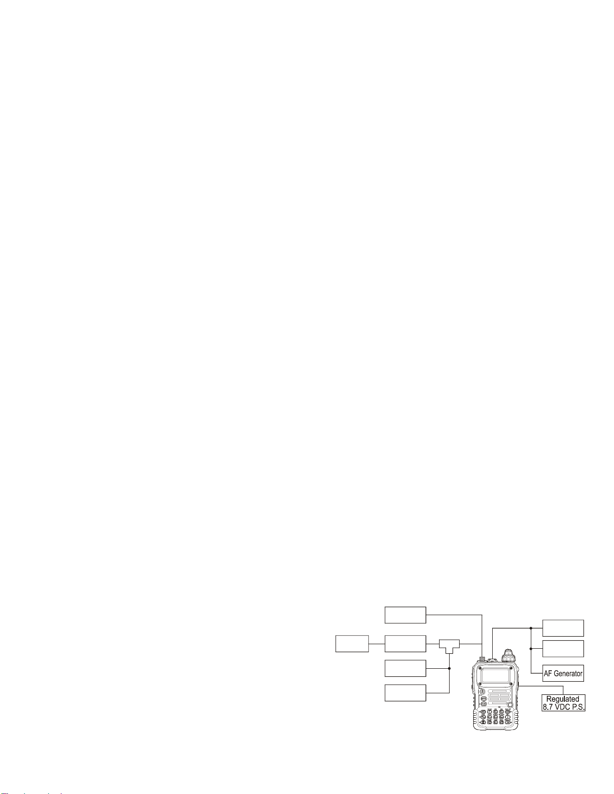
RF Signal
50-ohm
RF Load
Generator
In-Line
Wattmeter
Deviation
Meter
Sampling
Coupler
8-ohm
AF Load
SINAD
Meter
Frequency
Counter
DW
Alignment Setup
11

Alignment
Test Setup
Set up the test equipment as shown below for transceiv-
er alignment, and apply 8.7 V DC power to the transceiver.
Refer to the drawings for Alignment Points.
Internal System Alignment Routine
This uses a programmed routine in the transceiver
which simplifies many previously complex discrete com-
ponent settings and adjustments with digitally-controlled
settings via front panel buttons and LCD indications.
To begin, set the transceiver to the center of the 50 MHz,
144 MHz, 222 MHz and 430 MHz bands. Next, select the
430 MHz band, then turn the transceiver off.
Now, press and hold in the MON/F, and 0 buttons (at
the same time) while powering the radio on again. The
display will show the first setting. Thereafter, the frequen-
cies used during alignment will automatically be set with-
out action by the technician.
In the alignment process, each adjustment is selected
by rotating the DIAL. Alignment is performed by:
H Pressing the V/M button;
H Injecting a signal of the required frequency and lev-
el; then
H Pressing the V/M button after a level setting or ad-
justment is made. This second pressing of the MON/
F button stores the entry.
To exit the alignment routine, press the HM/RV button.
After performing the system alignment in its entirety, in-
dividual settings can be returned to and adjusted should
the need arise.
As each transceiver is individually optimized at the fac-
tory, the precise settings for the transceiver on your bench
may be slightly different.
Main Band Alignment
PLL Reference Frequency (PLL REF)
Press the V/M button, then transmit and adjust the counter
frequency to 440.000 (±300 Hz) by rotating the DIAL, then
press the V/M button. Rotate the DIAL to select the next
setting.
430 MHz band Alignment
Squelch Hysteresis Adjustment (HIS SQL)
H Rotate the DIAL for minimum squelch hysteresis. Press
the V/M button, then rotate the DIAL to select the next
setting.
12
Squelch Preset Threshold (THLD SQL) [86]
H Inject a –15.0 dBµ RF signal (1 kHz tone @ ±3.5 kHz
deviation), then press the V/M button, then press the
MON/F button twice. Press the V/M button, then rotate
the DIAL to select the next setting.
Squelch Preset Tight (TIGH SQL)
H Adjust the generator level to –5.0 dBµ, then press the V/
M button, then press the MON/F button twice. Press the
V/M button, then rotate the DIAL to select the next set-
ting.
S-Meter S-1 Adjustment (S1 LEVEL)
H Adjust the generator level to –7.0 dBµ (1 kHz tone @
±3.5 kHz deviation), then press the V/M button, then
press the MON/F button twice. Press the V/M button, then
rotate the DIAL to select the next setting.
S-Meter Full-Scale Adjustment (S9 LEVEL)
H Adjust the generator level to +19 dBµ (1 kHz tone @
±3.5 kHz deviation), then press the V/M button, then
press the MON/F button twice. Press the V/M button, then
rotate the DIAL to select the next setting.
Wide-FM S-Meter S-1 Adjustment (S1 LEVEL)
H Adjust the generator level to 0 dBµ (1 kHz tone @ ±20
kHz deviation), then press the V/M button, then press
the MON/F button twice. Press the V/M button, then ro-
tate the DIAL to select the next setting.
Wide-FM S-Meter Full-Scale Adjustment (S9 LEVEL)
H Adjust the generator level to +20 dBµ (1 kHz tone @ ±20
kHz deviation), then press the V/M button, then press
the MON/F button twice. Press the V/M button, then ro-
tate the DIAL to select the next setting.
The alignment frequency will now be automatically set
to 430.000 MHz.
High TX Power Adjustment (HI POWER)
H Transmit, and adjust the output power level for 5.0 W
(±0.3 W) by rotating the DIAL, then press the V/M but-
ton. Rotate the DIAL to select the next setting.
L3 Tx Power Adjustment (L3 POWER)
H Transmit, and adjust the output power level for 2.5 W
(±0.2 W) by rotating the DIAL, then press the V/M but-
ton. Rotate the DIAL to select the next setting.
L2 Tx Power Adjustment (L2 POWER)
H Transmit, and adjust the output power level for 1.0 W
(±0.1 W) by rotating the DIAL, then press the V/M but-
ton. Rotate the DIAL to select the next setting.

Alignment
L1 Tx Power Adjustment (L1 POWER)
H Transmit, and adjust the output power level for 50 mW
(+50/-30 mW) by rotating the DIAL, then press the V/M
button. Rotate the DIAL to select the next setting.
TX Deviation Adjustment (MAX DEV)
H Inject a 1 kHz audio tone at a level of 50 mV (rms) to the
MIC jack. Press the V/M button, then transmit and ad-
just the deviation for 4.5 kHz (±0.2 kHz) (USA Version:
4.2 kHz (±0.2 kHz)) by rotating the DIAL, then press the
V/M button. Rotate the DIAL to select the next setting.
CTCSS Tx Deviation Adjustment (TN 67.0)
H Press the V/M button, then transmit and adjust the de-
viation for 0.5 kHz (+0.05/-0.1 kHz) by rotating the DIAL,
then press the V/M button. Rotate the DIAL to select the
next setting.
CTCSS Tx Deviation Adjustment (TN 183.5)
H Press the V/M button, then transmit and adjust the de-
viation for 0.5 kHz (±0.1 kHz) by rotating the DIAL, then
press the V/M button. Rotate the DIAL to select the next
setting.
CTCSS Tx Deviation Adjustment (TN 254.1)
H Press the V/M button, then transmit and adjust the de-
viation for 0.5 kHz (±0.1 kHz) by rotating the DIAL, then
press the V/M button. Rotate the DIAL to select the next
setting.
DCS Tx Deviation Adjustment (DCS DEV)
H Press the V/M button, then transmit and adjust the de-
viation for 0.6 kHz (±0.1 kHz) by rotating the DIAL, then
press the V/M button. Rotate the DIAL to select the next
setting.
Press the MON/F to activate the TX Power and Devia-
tion alignment routine.
The alignment frequency will automatically be set to
440.000 MHz (USA Version: 450.000 MHz).
High TX Power Adjustment (L2 POWER)
H Transmit, and adjust the output power level for 1.0 W
(±0.1 W) by rotating the DIAL, then press the V/M but-
ton. Rotate the DIAL to select the next setting.
High TX Power Adjustment (L1 POWER)
H Transmit, and adjust the output power level for 50 mW
(+50/-30 mW) by rotating the DIAL, then press the V/M
button. Rotate the DIAL to select the next setting.
TX Deviation Adjustment (MAX DEV)
H Inject a 1 kHz audio tone at a level of 50mV (rms) to the
MIC jack. Press the V/M button, then transmit and adjust
the deviation for 4.5 kHz (±0.2 kHz) (USA Version: 4.2
kHz (±0.1 kHz)) by rotating the DIAL, then press the V/M
button. Rotate the DIAL to select the next setting.
CTCSS Tx Deviation Adjustment (TN 67.0)
H Press the V/M button, then transmit and adjust the de-
viation for 0.5 kHz (+0.05/-0.1 kHz) by rotating the DIAL,
then press the V/M button. Rotate the DIAL to select the
next setting.
CTCSS Tx Deviation Adjustment (TN 183.5)
H Press the V/M button, then transmit and adjust the de-
viation for 0.5 kHz (±0.1 kHz) by rotating the DIAL, then
press the V/M button. Rotate the DIAL to select the next
setting.
CTCSS Tx Deviation Adjustment (TN 254.1)
H Press the V/M button, then transmit and adjust the de-
viation for 0.5 kHz (±0.1 kHz) by rotating the DIAL, then
press the V/M button. Rotate the DIAL to select the next
setting.
DCS Tx Deviation Adjustment (DCS DEV)
H Press the V/M button, then transmit and adjust the de-
viation for 0.6 kHz (±0.1 kHz) (USA Version: 0.9 kHz
(±0.1 kHz)) by rotating the DIAL, then press the V/M
button. Rotate the DIAL to select the next setting.
High TX Power Adjustment (HI POWER)
H Transmit, and adjust the output power level for 5.0 W
(±0.3 W) by rotating the DIAL, then press the V/M but-
ton. Rotate the DIAL to select the next setting.
High TX Power Adjustment (L3 POWER)
H Transmit, and adjust the output power level for 2.5 W
(±0.2 W) by rotating the DIAL, then press the V/M but-
ton. Rotate the DIAL to select the next setting.
Press the BAND button to activate the 50 MHz band
internal alignment routine.
The alignment frequency will automatically be set to
52.100 MHz.
50 MHz Band Alignment
Squelch Hysteresis Adjustment (HIS SQL)
H Rotate the DIAL for minimum squelch hysteresis. Press
the V/M button, then rotate the DIAL to select the next
setting.
13

Alignment
Squelch Preset Threshold (THLD SQL)
H Inject a –15.0 dBµ RF signal (1 kHz tone @ ±3.5 kHz
deviation), then press the V/M button, then press the
MON/F button twice. Press the V/M button, then rotate
the DIAL to select the next setting.
Squelch Preset Tight (TIGH SQL)
H Adjust the generator level to –4.0 dBµ, then press the V/M
button, then press the MON/F button twice. Press the V/M
button, then rotate the DIAL to select the next setting.
S-Meter S-1 Adjustment (S1 LEVEL)
H Adjust the generator level to –7.0 dBµ (1 kHz tone @
±3.5 kHz deviation), then press the V/M button, then
press the MON/F button twice. Press the V/M button, then
rotate the DIAL to select the next setting.
S-Meter Full-Scale Adjustment (S9 LEVEL)
H Adjust the generator level to +19 dBµ (1 kHz tone @
±3.5 kHz deviation), then press the V/M button, then
press the MON/F button twice. Press the V/M button, then
rotate the DIAL to select the next setting.
Wide-FM S-Meter S-1 Adjustment (S1 LEVEL)
H Adjust the generator level to 0 dBµ (1 kHz tone @ ±20
kHz deviation), then press the V/M button, then press
the MON/F button twice. Press the V/M button, then ro-
tate the DIAL to select the next setting.
Wide-FM S-Meter Full-Scale Adjustment (S9 LEVEL)
H Adjust the generator level to +20 dBµ (1 kHz tone @ ±20
kHz deviation), then press the V/M button, then press
the MON/F button twice. Press the V/M button, then ro-
tate the DIAL to select the next setting.
The alignment frequency will now be automatically set
to 50.000 MHz.
L1 Tx Power Adjustment (L1 POWER)
H Transmit, and adjust the output power level for 50 mW
(+50/-30 mW) by rotating the DIAL, then press the V/M
button. Rotate the DIAL to select the next setting.
TX Deviation Adjustment (MAX DEV)
H Inject a 1 kHz audio tone at a level of 50mV (rms) to the
MIC jack. Press the V/M button, then transmit and adjust
the deviation for4.5 kHz (±0.2 kHz) (USA Version: (4.2
±0.2 kHz)) by rotating the DIAL, then press the V/M but-
ton. Rotate the DIAL to select the next setting.
AM Modulation (AM MOD)
H Inject a 1 kHz audio tone at a level of 100 mV (rms) to
the MIC jack. Press the V/M button, then transmit and
adjust the modulation for 60% (±10%) by rotating the
DIAL, then press and hold in the MON/F button for one
second.
CTCSS Tx Deviation Adjustment (TN 67.0)
H Press the V/M button, then transmit and adjust the de-
viation for 0.6 kHz (+0.05/-0.1 kHz) by rotating the DIAL,
then press the V/M button. Rotate the DIAL to select the
next setting.
CTCSS Tx Deviation Adjustment (TN 167.9)
H Press the V/M button, then transmit and adjust the de-
viation for 0.6 kHz (+0.05/-0.1 kHz) by rotating the DIAL,
then press the V/M button. Rotate the DIAL to select the
next setting.
CTCSS Tx Deviation Adjustment (TN 254.1)
H Press the V/M button, then transmit and adjust the de-
viation for 0.6 kHz (+0.05/-0.1 kHz) by rotating the DIAL,
then press the V/M button. Rotate the DIAL to select the
next setting.
High TX Power Adjustment (HI POWER)
H Transmit, and adjust the output power level for 5.0 W
(±0.3 W) by rotating the DIAL, then press the V/M but-
ton. Rotate the DIAL to select the next setting.
L3 Tx Power Adjustment (L3 POWER)
H Transmit, and adjust the output power level for 2.5 W
(±0.2 W) by rotating the DIAL, then press the V/M but-
ton. Rotate the DIAL to select the next setting.
L2 Tx Power Adjustment (L2 POWER)
H Transmit, and adjust the output power level for 1.0 W
(±0.1 W) by rotating the DIAL, then press the V/M but-
ton. Rotate the DIAL to select the next setting.
14
DCS Tx Deviation Adjustment (DCS DEV)
H Press the V/M button, then transmit and adjust the de-
viation for 0.6 kHz (±0.1 kHz) by rotating the DIAL, then
press the V/M button. Rotate the DIAL to select the next
setting.
Press the MON/F button to activate the TX Power and
Deviation alignment routine.
The alignment frequency will automatically be set to
54.000 MHz.
High TX Power Adjustment (HI POWER)
H Transmit, and adjust the output power level for 5.0 W
(±0.3 W) by rotating the DIAL, then press the V/M but-
ton. Rotate the DIAL to select the next setting.

Alignment
High TX Power Adjustment (L3 POWER)
H Transmit, and adjust the output power level for 2.5 W
(±0.2 W) by rotating the DIAL, then press the V/M but-
ton. Rotate the DIAL to select the next setting.
High TX Power Adjustment (L2 POWER)
H Transmit, and adjust the output power level for 1.0 W
(±0.1 W) by rotating the DIAL, then press the V/M but-
ton. Rotate the DIAL to select the next setting.
High TX Power Adjustment (L1 POWER)
H Transmit, and adjust the output power level for 50 mW
(+50/-30 mW) by rotating the DIAL, then press the V/M
button. Rotate the DIAL to select the next setting.
TX Deviation Adjustment (MAX DEV)
H Inject a 1 kHz audio tone at a level of 50mV (rms) to the
MIC jack. Press the V/M button, then transmit and ad-
just the deviation for 4.5 kHz (±0.2 kHz) (USA Version:
4.2 kHz (±0.2 kHz)) by rotating the DIAL, then press the
V/M button. Rotate the DIAL to select the next setting.
AM Modulation (AM MOD)
H Inject a 1 kHz audio tone at a level of 100mV (rms) to
the MIC jack. Press the V/M button, then transmit and
adjust the modulation for 60% (±10%) by rotating the
DIAL.
CTCSS Tx Deviation Adjustment (TN 67.0)
H Press the V/M button, then transmit and adjust the de-
viation for 0.6 kHz (+0.05/-0.1 kHz) by rotating the DIAL,
then press the V/M button. Rotate the DIAL to select the
next setting.
CTCSS Tx Deviation Adjustment (TN 167.9)
H Press the V/M button, then transmit and adjust the de-
viation for 0.6 kHz (+0.05/-0.1 kHz) by rotating the DIAL,
then press the V/M button. Rotate the DIAL to select the
next setting.
CTCSS Tx Deviation Adjustment (TN 254.1)
H Press the V/M button, then transmit and adjust the de-
viation for 0.6 kHz (+0.05/-0.1 kHz) by rotating the DIAL,
then press the V/M button. Rotate the DIAL to select the
next setting.
DCS Tx Deviation Adjustment (DCS DEV)
H Press the V/M button, then transmit and adjust the de-
viation for 0.6 kHz (±0.1 kHz) by rotating the DIAL, then
press the V/M button. Rotate the DIAL to select the next
setting.
Press the BAND button to activate the 145 MHz band
internal alignment routine.
The alignment frequency will automatically be set to
145.100 MHz (USA Version: 146.100 MHz).
144 MHz Band Alignment
Squelch Hysteresis Adjustment (HIS SQL)
H Rotate the DIAL for minimum squelch hysteresis. Press
the V/M button, then rotate the DIAL to select the next
setting.
Squelch Preset Threshold (THLD SQL)
H Inject a –15.0 dBµ RF signal (1 kHz tone @ ±3.5 kHz
deviation), then press the V/M button, then press the
MON/F button twice. Press the V/M button, then rotate
the DIAL to select the next setting.
Squelch Preset Tight (TIGH SQL)
H Adjust the generator level to –4.0 dBµ, then press the V/
M button, then press the MON/F button twice. Press the
V/M button, then rotate the DIAL to select the next set-
ting.
S-Meter S-1 Adjustment (S1 LEVEL)
H Adjust the generator level to –7.0 dBµ (1 kHz tone @
±3.5 kHz deviation), then press the V/M button, then
press the MON/F button twice. Press the V/M button, then
rotate the DIAL to select the next setting.
S-Meter Full-Scale Adjustment (S9 LEVEL)
H Adjust the generator level to +19 dBµ (1 kHz tone @
±3.5 kHz deviation), then press the V/M button, then
press the MON/F button twice. Press the V/M button, then
rotate the DIAL to select the next setting.
Wide-FM S-Meter S-1 Adjustment (S1 LEVEL)
H Adjust the generator level to 0 dBµ (1 kHz tone @ ±20
kHz deviation), then press the V/M button, then press
the MON/F button twice. Press the V/M button, then ro-
tate the DIAL to select the next setting.
Wide-FM S-Meter Full-Scale Adjustment (S9 LEVEL)
H Adjust the generator level to +20 dBµ (1 kHz tone @ ±20
kHz deviation), then press the V/M button, then press
the MON/F button twice. Press the V/M button, then ro-
tate the DIAL to select the next setting.
The alignment frequency will now be automatically set
to 144.000 MHz.
15

Alignment
High TX Power Adjustment (HI POWER)
H Transmit, and adjust the output power level for 5.0 W
(±0.3 W) by rotating the DIAL, then press the V/M but-
ton. Rotate the DIAL to select the next setting.
L3 Tx Power Adjustment (L3 POWER)
H Transmit, and adjust the output power level for 2.5 W
(±0.2 W) by rotating the DIAL, then press the V/M but-
ton. Rotate the DIAL to select the next setting.
L2 Tx Power Adjustment (L2 POWER)
H Transmit, and adjust the output power level for 1.0 W
(±0.1 W) by rotating the DIAL, then press the V/M but-
ton. Rotate the DIAL to select the next setting.
L1 Tx Power Adjustment (L1 POWER)
H Transmit, and adjust the output power level for 50 mW
(+50/-30 mW) by rotating the DIAL, then press the V/M
button. Rotate the DIAL to select the next setting.
TX Deviation Adjustment (MAX DEV)
H Inject a 1 kHz audio tone at a level of 50mV (rms) to the
MIC jack. Press the V/M button, then transmit and ad-
just the deviation for 4.5 kHz (±0.2 kHz) (USA Version:
4.2 kHz (±0.2 kHz)) by rotating the DIAL, then press the
V/M button. Rotate the DIAL to select the next setting.
CTCSS Tx Deviation Adjustment (TN 67.0)
H Press the V/M button, then transmit and adjust the de-
viation for 0.6 kHz (+0.05/-0.1 kHz) by rotating the DIAL,
then press the V/M button. Rotate the DIAL to select the
next setting.
CTCSS Tx Deviation Adjustment (TN 151.4)
H Press the V/M button, then transmit and adjust the de-
viation for 0.6 kHz (+0.05/-0.1 kHz) by rotating the DIAL,
then press the V/M button. Rotate the DIAL to select the
next setting.
CTCSS Tx Deviation Adjustment (TN 254.1)
H Press the V/M button, then transmit and adjust the de-
viation for 0.6 kHz (+0.05/-0.1 kHz) by rotating the DIAL,
then press the V/M button. Rotate the DIAL to select the
next setting.
DCS Tx Deviation Adjustment (DCS DEV)
H Press the V/M button, then transmit and adjust the de-
viation for 0.6 kHz (±0.1 kHz) by rotating the DIAL, then
press the V/M button. Rotate the DIAL to select the next
setting.
Press the MON/F to activate the TX Power and Devia-
tion alignment routine.
The alignment frequency will automatically be set to
146.000 MHz (USA Version: 148.000 MHz).
High TX Power Adjustment (HI POWER)
H Transmit, and adjust the output power level for 5.0 W
(±0.3 W) by rotating the DIAL, then press the V/M but-
ton. Rotate the DIAL to select the next setting.
High TX Power Adjustment (L3 POWER)
H Transmit, and adjust the output power level for 2.5 W
(±0.2 W) by rotating the DIAL, then press the V/M but-
ton. Rotate the DIAL to select the next setting.
High TX Power Adjustment (L2 POWER)
H Transmit, and adjust the output power level for 1.0 W
(±0.1 W) by rotating the DIAL, then press the V/M but-
ton. Rotate the DIAL to select the next setting.
High TX Power Adjustment (L1 POWER)
H Transmit, and adjust the output power level for 50 mW
(+50/-30 mW) by rotating the DIAL, then press the V/M
button. Rotate the DIAL to select the next setting.
TX Deviation Adjustment (MAX DEV)
H Inject a 1 kHz audio tone at a level of 50mV (rms) to the
MIC jack. Press the V/M button, then transmit and ad-
just the deviation for 4.5 kHz (±0.2 kHz) (USA Version:
4.2 kHz (±0.2 kHz)) by rotating the DIAL, then press the
V/M button. Rotate the DIAL to select the next setting.
CTCSS Tx Deviation Adjustment (TN 67.0)
H Press the V/M button, then transmit and adjust the de-
viation for 0.6 kHz (+0.05/-0.1 kHz) by rotating the DIAL,
then press the V/M button. Rotate the DIAL to select the
next setting.
CTCSS Tx Deviation Adjustment (TN 151.4)
H Press the V/M button, then transmit and adjust the de-
viation for for 0.6 kHz (+0.05/-0.1 kHz) by rotating the
DIAL, then press the V/M button. Rotate the DIAL to
select the next setting.
CTCSS Tx Deviation Adjustment (TN 254.1)
H Press the V/M button, then transmit and adjust the de-
viation for 0.6 kHz (+0.05/-0.1 kHz) by rotating the DIAL,
then press the V/M button. Rotate the DIAL to select the
next setting.
16

Alignment
DCS Tx Deviation Adjustment (DCS DEV)
H Press the V/M button, then transmit and adjust the de-
viation for 0.6 kHz (±0.1 kHz) by rotating the DIAL, then
press the V/M button. Rotate the DIAL to select the next
setting.
NOTE: The next step depends on the geographical "version" of
the transceiver being aligned:
EXP Version: Alignment of the "SUB Band " follows (see
page 18.)
USA Version: Press the BAND button to activate the
222 MHz band internal alignment routine. In this case,
the alignment frequency will automatically be set to
222.000 MHz.
222 MHz Band Alignment
L2 Tx Power Adjustment (L2 POWER)
H Transmit, and adjust the output power level for 0.3 W
(±0.1 W) by rotating the DIAL, then press the V/M but-
ton. Rotate the DIAL to select the next setting.
L1 Tx Power Adjustment (L1 POWER)
H Transmit, and adjust the output power level for 50 mW
(+50/-30 mW) by rotating the DIAL, then press the V/M
button. Rotate the DIAL to select the next setting.
DCS Tx Deviation Adjustment (DCS DEV)
H Press the V/M button, then transmit and adjust the de-
viation for 0.9 kHz (±0.1 kHz) by rotating DIAL, then
press the V/M button. Rotate the DIAL to select the next
setting.
Press the
to activate the TX Power and Devia-
tion alignment routine.
The alignment frequency will automatically be set to
224.995 MHz.
High Tx Power Adjustment (L2 POWER)
H Transmit, and adjust the output power level for 0.3 W
(+0.2/-0.1 W) by rotating the DIAL, then press the V/M
button. Rotate the DIAL to select the next setting.
High Tx Power Adjustment (L1 POWER)
H Transmit, and adjust the output power level for 50 mW
(+50/-30 mW) by rotating the DIAL, then press the V/M
button. Rotate the DIAL to select the next setting.
TX Deviation Adjustment (MAX DEV)
H Inject a 1 kHz audio tone at a level of 50mV (rms) to the
MIC jack. Press the V/M button, then transmit and ad-
just the deviation for 4.5 kHz (±0.2 kHz) (USA Version:
4.2 kHz (±0.2 kHz) by rotating DIAL, then press the V/
M button. Rotate the DIAL to select the next setting.
TX Deviation Adjustment (MAX DEV)
H Inject a 1 kHz audio tone at a level of 50mV (rms) to the
MIC jack. Press the V/M button, then transmit and ad-
just the deviation for 4.5 kHz (±0.2 kHz) (USA Version:
4.2 kHz (±0.2 kHz)) by rotating the DIAL, then press the
V/M button. Rotate the DIAL to select the next setting.
CTCSS Tx Deviation Adjustment (TN 67.0)
H Press the V/M button, then transmit and adjust the de-
viation for 0.6 kHz (+0.05/-0.1 kHz) by rotating the DIAL,
then press the V/M button. Rotate the DIAL to select the
next setting.
CTCSS Tx Deviation Adjustment (TN 151.4)
H Press the V/M button, then transmit and adjust the de-
viation for 0.6 kHz (+0.05/-0.1 kHz) by rotating the DIAL,
then press the V/M button. Rotate the DIAL to select the
next setting.
CTCSS Tx Deviation Adjustment (TN 254.1)
H Press the V/M button, then transmit and adjust the de-
viation for 0.6 kHz (+0.05/-0.1 kHz) by rotating the DIAL,
then press the V/M button. Rotate the DIAL to select the
next setting.
CTCSS Tx Deviation Adjustment (TN 67.0)
H Press the V/M button, then transmit and adjust the de-
viation for 0.6 kHz (+0.05/-0.1 kHz) by rotating the DIAL,
then press the V/M button. Rotate the DIAL to select the
next setting.
CTCSS Tx Deviation Adjustment (TN 151.4)
H Press the V/M button, then transmit and adjust the de-
viation for 0.6 kHz (+0.05/-0.1 kHz) by rotating the
DIAL, then press the V/M button. Rotate the DIAL to
select the next setting.
CTCSS Tx Deviation Adjustment (TN 254.1)
H Press the V/M button, then transmit and adjust the de-
viation for 0.6 kHz (+0.05/-0.1 kHz) by rotating the DIAL,
then press the V/M button. Rotate the DIAL to select the
next setting.
DCS Tx Deviation Adjustment (DCS DEV)
H Press the V/M button, then transmit and adjust the de-
viation for 0.9 kHz (±0.1 kHz) by rotating the DIAL, then
press the V/M button. Rotate the DIAL to select the next
setting.
17

Alignment
Press the SUB button to activate the SUB band internal
alignment routine.
The alignment frequency will automatically be set to
435.100 MHz (USA Version: 440.100 MHz) on the SUB
band.
SUB Band Alignment
430 MHz Band Alignment
Squelch Hysteresis Adjustment (HIS SQL)
H Rotate the DIAL for minimum squelch hysteresis. Press
the V/M button, then rotate the DIAL to select the next
setting.
Squelch Preset Threshold (THLD SQL)
H Inject a –13.0 dBµ RF signal (1 kHz tone @ ±3.5 kHz
deviation), then press the V/M button, then press the
MON/F button twice. Press the V/M button, then rotate
the DIAL to select the next setting.
Squelch Preset Tight (TIGH SQL)
H Adjust the generator level to –6.0 dBµ, then press the V/M
button, then press the MON/F button twice. Press the V/M
button, then rotate the DIAL to select the next setting.
S-Meter S-1 Adjustment (S1 LEVEL)
H Adjust the generator level to –7.0 dBµ (1 kHz tone @
±3.5 kHz deviation), then press the V/M button, then
press the MON/F button twice. Press the V/M button, then
rotate the DIAL to select the next setting.
S-Meter Full-Scale Adjustment (S9 LEVEL)
H Adjust the generator level to +20 dBµ (1 kHz tone @
±3.5 kHz deviation), then press the V/M button, then
press the MON/F button twice. Press the V/M button.
Press the BAND button to activate the 50 MHz SUB band
internal alignment routine.
The alignment frequency will automatically be set to
52.100 MHz.
50 MHz SUB Band Alignment
Squelch Hysteresis Adjustment (HIS SQL)
H Rotate the DIAL for minimum squelch hysteresis. Press
the V/M button, then rotate the DIAL to select the next
setting.
Squelch Preset Threshold (THLD SQL)
H Inject a –13.0 dBµ RF signal (1 kHz tone @ ±3.5 kHz
deviation), then press the V/M button, then press the
MON/F button twice. Press the V/M button, then rotate
the DIAL to select the next setting.
Squelch Preset Tight (TIGH SQL)
H Adjust the generator level to –4.0 dBµ, then press the V/
M button, then press the MON/F button twice. Press the
V/M button, then rotate the DIAL to select the next set-
ting.
S-Meter S-1 Adjustment (S1 LEVEL)
H Adjust the generator level to –7.0 dBµ (1 kHz tone @
±3.5 kHz deviation), then press the V/M button, then
press the MON/F button twice. Press the V/M button, then
rotate the DIAL to select the next setting.
S-Meter Full-Scale Adjustment (S9 LEVEL)
H Adjust the generator level to +19 dBµ (1 kHz tone @
±3.5 kHz deviation), then press the V/M button, then
press the MON/F button twice. Press the V/M button.
Press the BAND button to activate the 144 MHz SUB band
internal alignment routine.
The alignment frequency will automatically be set to
145.100 MHz (USA Version: 146.100 MHz).
144 MHz SUB Band Alignment
Squelch Hysteresis Adjustment (HIS SQL)
H Rotate the DIAL for minimum squelch hysteresis. Press the
V/M button, then rotate the DIAL to select the next setting.
Squelch Preset Threshold (THLD SQL)
H Inject a –15.0 dBµ RF signal (1 kHz tone @ ±3.5 kHz
deviation), then press the V/M button, then press the
MON/F button twice. Press the V/M button, then rotate
the DIAL to select the next setting.
Squelch Preset Tight (TIGH SQL)
H Adjust the generator level to –6.0 dBµ, then press the V/M
button, then press the MON/F button twice. Press the V/M
button, then rotate the DIAL to select the next setting.
S-Meter S-1 Adjustment (S1 LEVEL)
H Adjust the generator level to –7.0 dBµ (1 kHz tone @
±3.5 kHz deviation), then press the V/M button, then
press the MON/F button twice. Press the V/M button, then
rotate the DIAL to select the next setting.
S-Meter Full-Scale Adjustment (S9 LEVEL)
H Adjust the generator level to +19 dBµ (1 kHz tone @
±3.5 kHz deviation), then press the V/M button, then
presses the MON/F button twice. Press the V/M button.
This completes the internal alignment routine for all bands.
To save all settings and exit, press the HM/RV button.
18

Circuit Diagram
800M RX:0.8V
MAIN NFM RX:+14.7dBµ
435.000MHz, @12dB SINAD
1000pF Coupling Capacitor.
800M RX:1.87V
0V
(50M TX:1.84V)
(144M TX:1.85V)
(430M TX:2.85V)
RF Unit (Lot. 1~)
MAIN NFM RX:+2.0dBµ
435.000MHz
1000pF Coupling Capacitor.
430M RX:0.79V (0V)
MAIN NFM RX:+11.5dBµ
SUB NFM RX:+7.1dBµ
145.000MHz
1000pF Coupling Capacitor.
MAIN NFM RX:+4.3dBµ
SUB NFM RX:+3.5dBµ
52.000MHz
1000pF Coupling Capacitor.
0.8V (0V)
0.7V (0V)
50M RX:0.8V
430M RX:1.05V (0V)
76~222M RX:1.81V (0V)
50M RX:1.13V (0V)
800M RX:1.61V
430M RX:
0.81V
(0V)
SUB430M RX:0.83V (0V)
800M RX:0.73V
430M RX:1.89V
(0V)
SUB430M RX:1.57V (0V)
50M RX:0.67V (0V)
430M RX:0.66V
(0V)
76~222M RX:1.83V (0V)
76~222M RX:
0.73V (0V)
SUB144M RX:2.4V (0V)
50M RX:2.0V (0V)
MAIN NFM RX:+7.3dBµ
435.000MHz
1000pF Coupling Capacitor.
430M RX:1.77V
(0V)
SUB430M RX:
2.14V (0V)
SUB NFM RX:+5.7dBµ
435.000MHz
1000pF Coupling Capacitor.
BC SW RX:0.79V
50M RX:1.31V
50M TX:3.9V
0V (0V)
0V
(1.98V)
0V
(1.24V)
0V
0V
(5.22V)
(2.27V)
0V (2.28V)
1.0V
(2.4V)
0.7V
(0.7V)
76~222M RX:1.37V
76~222M TX:1.08V
76~222M RX:0.6V
76~222M TX:0.2V
50M RX:0.35V
50M TX:0.45V
145M TX:+5.1dBm
430M TX:+6.9dBm
1000pF Coupling Capacitor.
0V
(3.97V)
0V (0V)
1.88V
(1.92V)
0V
(50M:0.8V)
(144M:0.82V)
(430M:1.29V)
0V
(50M:1.12V)
0V
(50M:0.84V)
(144M:0.82V)
(430M:1.29V)
0V
(1.86V)
0V
(50M:0.88V)
(144M:0.88V)
(430M:1.32V)
0V
(50M:0.86V)
(144M:0.86V)
(430M:1.32V)
0V
(50M:2.44V)
13.5V
(13.3V)
0V
(50M:1.75V)
(144M:2.37V)
(430M:2.52V)
0V (50M TX:4.51V)
50M TX:+15.7dBm
1000pF Coupling Capacitor.
0V
(1.42V)
0V
(50M:1.5V)
(144M:2.2V)
(430M:1.7V)
0V (0V)
AM RX:2.61V
13.8V
(13.6V)
BC SW RX:0.78V
BC SW RX:0.75V
AM RX:+12dBµ
10dB SN
0.1µF Coupling Capacitor.
0V (0V)
SW RX:2.95V
0V~6.43V (0V)
SUB50M RX:1.27V (0V)
BC SW RX:0.59V
BC SW RX:1.5V
0V (0V)
1.3V
(1.3V)
2.3V
(2.3V)
0.66V
(0.66V)
2.9V
(2.9V)
6.47V
(6.47V)
1.32V
(1.32V)
2.9V (2.9V)
UL:0V
0V (0V)
UL:2.9V
6.4V
(6.4V)
0V (2.9V)
(AMTX:2.38V)
0V (0V)
AM:2.5V
(AM:2.5V)
0V (2.5V)
(AMTX:0V)
0V (0V)
0V (2.9V)
AMRX:1.84V
(AMTX:2.9V)
0V (0V)
0V (0.48V)
0V (0V)
0V (4.85V)
0V (0V)
0V (0V)
0V (2.9V)
2.25V (2.3V)
2.98V
(3.03V)
2.93V
(2.98V)
0V (2.4V)
50M: 2.77V
SHIFT ON:2.86V
SHIFT OFF:0V
1.55V (1.6V)
SAVE:2.94V
2.25V
(1.6V)
(0.48V)
2.12V
SAVE:0V
2.26V
(2.81V)
0V (2.95V)
2.78V (0V)
50M: 1.99V
(2.07V)
0V (5.5V)
50M RX:0V
0V (0V)
50M RX:0.45V
13.4V
(13.3V)
12.8V
(12.7V)
76~222M RX:1.98V
76~222M TX:2.05V
430M: 1.99V
0.2V (0V)
430M RX:2.13V
0.66V (0V)
430M RX:2.7V
(2.01V)
EXT DC IN 13.8V
:RX, (**):TX
**
19
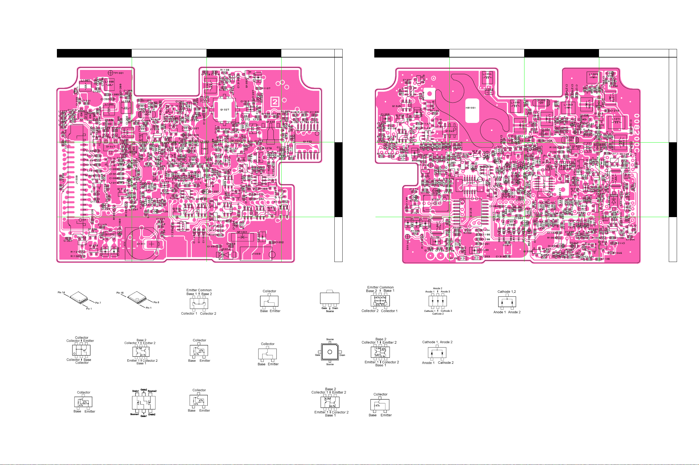
RF Unit (Lot. 1~)
Parts Layout
AC
B
D
1
2
acb
d
1
2
NJM12902V
(Q1022)
CPH6102 (AB)
(Q1043)
DTA144EE (16)
(Q1021)
MB15A01PFV1
(Q1019)
UMD6N (D6)
(Q1015)
HN1J02FU (KS)
(Q1031)
UMW1 (W1)
(Q1044)
DTC143ZE (E23)
(Q1025)
DTC144EE (26)
(Q1001, 1026, 1029,
1030, 1034, 1035,
1042, 1051, 1053)
2SA1774 (FR)
(Q1033, 1036, 1038,
1046, 1052)
2SC4154E (LE)
(Q1032)
2SC5226 (LN)
(Q1014, 1024)
2SC5277 (D2)
(Q1002, 1010)
2SC5374 (NA)
(Q1016, 1017, 1018)
2SC4915 (QY)
(Q1008, 1009, 1013,
1020)
2SC5555ZD (ZD-)
(Q1003, 1004, 1005,
1006, 1007, 1011,
1012)
3
Side A
2SK3475
(Q1023)
2SK3476
(Q1027)
KRA760U-RTK
(Q1028, 1037, 1039,
1041, 1045, 1050)
KRC654U-RTK
(Q1040, 1048, 1049)
KRA755U-RTK
(Q1047)
DTC144TE-TL
(Q1054)
HN2D01FU (A1)
(D1045, 1046)
1SS362 (C3)
(D1001, 1002, 1003)
1SS321 (F9)
(D1047)
DAN222 (N)
(D1006, 1007, 1008,
1009, 1010, 1011,
1012, 1027, 1028,
1041, 1043, 1044,
1063)
1SS385 (09)
(D1050)
3
Side B
20
 Loading...