

Page 1

SP701 Evaluaon Board
User Guide
UG1319 (v1.0) July 12, 2019
Page 2

Revision History
Send Feedback
The following table shows the revision history for this document.
Revision History
Section
07/12/2019 Version 1.0
Initial release. N/A
Revision Summary
UG1319 (v1.0) July 12, 2019 www.xilinx.com
SP701 Board User Guide 2
Page 3

Table of Contents
Send Feedback
Revision History...............................................................................................................2
Chapter 1: Introduction.............................................................................................. 4
Overview.......................................................................................................................................4
Additional Resources.................................................................................................................. 5
Block Diagram..............................................................................................................................5
Board Features............................................................................................................................ 6
Board Specifications....................................................................................................................7
Chapter 2: Board Setup and Configuration......................................................9
Electrostatic Discharge Caution.................................................................................................9
Board Components..................................................................................................................... 9
Default Switch and Jumper Settings....................................................................................... 12
Spartan-7 Device Configuration.............................................................................................. 13
Chapter 3: Board Component Descriptions................................................... 15
Overview.....................................................................................................................................15
Component Descriptions......................................................................................................... 15
UG1319 (v1.0) July 12, 2019 www.xilinx.com
SP701 Board User Guide 3
Appendix A: VITA 57.1 FMC Connector Pinouts............................................44
Appendix B: Xilinx Design Constraints............................................................. 45
Overview.....................................................................................................................................45
Appendix C: Regulatory and Compliance Information........................... 46
CE Information...........................................................................................................................46
Compliance Markings............................................................................................................... 47
Appendix D: Additional Resources and Legal Notices.............................48
Xilinx Resources.........................................................................................................................48
Documentation Navigator and Design Hubs.........................................................................48
References..................................................................................................................................49
Please Read: Important Legal Notices................................................................................... 50
Page 4

Introduction
Send Feedback
Overview
Chapter 1: Introduction
Chapter 1
The SP701 evaluaon board is based on the XC7S100FGGA676 device, a member of the Xilinx
7 series FPGA family. It is opmized for low cost, low power, and high I/O performance. It comes
with advanced high-performance FPGA logic based on real6-input look up table (LUT), 36 Kb
dual-port block RAM, support for DDR3L interface up to 1866 Mb/s, XADC with 12-bit
1 MSPA ADC with on-chip thermal and supply sensors, and powerful clock management les
(CMTs). The board is designed for high-performance and lower power with a 28 nm, 1V core
voltage process. For lower power, it has a 0.9V core voltage opon.
Table 1: XC7S100 Resources
Spartan®-7 FPGA
Resources
Logic Resources Part Number XCS7100
Logic Cells 102,400
Slices 16,000
CLB Flip-flops 128,000
Memory Resources Max. Distributed RAM (Kb) 1,100
Block RAM/FIFO w/EEC (36 Kb each) 120
Total Block RAM (Kb) 4,320
Clock Resources Clock Mgmt. Tiles (1 MMCM + 1 PLL) 8
I/O Resources Max. Single-Ended I/O Pins 400
Max. Differential I/O Pins 192
Embedded Hard IP
Resources
Speed Grades Commercial Temp (C) -1, -2
DSP Slices 160
Analog Mixed Signal (AMS)/XADC 1
Configuration AES/HMAC Blocks 1
Industrial Temp (I) -1, -2, -1L
Expanded Temp (Q) -1
Component Features
®
UG1319 (v1.0) July 12, 2019 www.xilinx.com
SP701 Board User Guide 4
Package Body Area (mm) Ball Pitch (mm) Available User I/O:
3.3V SelectIO™
technology HR I/O
FGGA676 27 x 27 1.0 400
Page 5

The following table lists the models for this board. See the SP701 evaluaon board product page
Send Feedback
for details.
Table 2: Models of SP701 Boards
Kit Description
EK-S7-SP701-G Xilinx Spartan-7 FPGA SP701 Evaluation Kit
EK-S7-SP701-G-J Xilinx Spartan-7 FPGA SP701 Evaluation Kit, Japan Specific
Additional Resources
See Appendix D: Addional Resources and Legal Noces for references to documents, les, and
resources relevant to the SP701 evaluaon board.
Chapter 1: Introduction
Block Diagram
The following gure shows the various components of the SP701 Evaluaon Board.
Figure 1: SP701 Evaluation Board Block Diagram
UG1319 (v1.0) July 12, 2019 www.xilinx.com
SP701 Board User Guide 5
Page 6

Board Features
Send Feedback
The SP701 evaluaon board features are listed here. Detailed informaon for each feature is
provided in Chapter 3: Board Component Descripons.
• XC7S100-2FGGA676 package
• Form factor: 6.00 in (152.4 mm) square, 0.08844 in (88.44 mils) thick
• Conguraon:
○ Quad SPI (QSPI) 1 Gb
○ Direct QSPI ash program header
○ USB-to-JTAG bridge
• DDR3L SDRAM memory:
○ 256Mx16 4 Gb DDR3-1866
Chapter 1: Introduction
• 32 Kb I2C EEPROM for hardware ID storage accessible by FPGA and System Controller
• Clocks:
○ I2C programmable SYSCLK oscillator 33.33 MHz
• VITA 57.1 FMC-LPC connector:
○ 34 dierenal pairs or 68 single-ended LA[00-33] bus
• 2x 10/100/1000 Tri-Speed Ethernet PHY
• Mobile industry processor interface (MIPI) features:
○ MIPI-CSI Camera Serial Interface (for PCAM 5C from Digilent)
○ MIPI-DSI Display Serial Interface
• HDMI output (1.4 specicaon support)
• USB-UART interface:
○ FT4232H JTAG/3xUART
• System Controller (MSP430)
• I2C Bus
UG1319 (v1.0) July 12, 2019 www.xilinx.com
SP701 Board User Guide 6
• 6x Pmod rt-angle receptacle (Digilent Pmod IF 1.2.0 specicaon support)
• General purpose I/O (GPIO):
○ 8x LED (GPIO_LED[0:7]) (acve-High)
○ 5x pushbuon switch, geographical, GPIO_SW_[N,E,S,W,C] (acve-High)
Page 7

○ 1x pushbuon switch, CPU_RESET (acve-High)
Send Feedback
○ 2x 8-pole DIP switch, GPIO_DIP_SW_B[0:15] (acve-High)
• Operaonal Switches:
○ Power On-O slide switch
○ PROG_B pushbuon switch (acve-Low)
○ 4-pole conguraon mode DIP switch M[0:2]_0_SW, INIT_B_0 (acve-Low)
• Operaonal Status LEDs:
○ Done
○ Power On
○ PG (Power Good)
• Power System:
Chapter 1: Introduction
○ V
○ I2C telemetry on 12V input and V
0.90V or 1.00V (I2C selectable)
ccint
Board Specifications
Dimensions
• Height: 6.00 in (152.4 mm)
• Width: 6.00 in (152.4 mm)
• Thickness: 0.08844 in (88.44 mils)
Note: A 3D model of this board is not available.
See the SP701 board website documentaon tab (Board Files check box) for the XDC lisng and
board schemacs (0381874).
Environmental
ccint
UG1319 (v1.0) July 12, 2019 www.xilinx.com
SP701 Board User Guide 7
• Temperature
○ Operang: 0°C to +45°C
○ Storage: –25°C to +60°C
• Humidity
○ 10% to 90% non-condensing
Page 8

Operating Voltage
Send Feedback
Chapter 1: Introduction
• +12V
DC
UG1319 (v1.0) July 12, 2019 www.xilinx.com
SP701 Board User Guide 8
Page 9

Chapter 2
Send Feedback
Board Setup and Configuration
Electrostatic Discharge Caution
CAUTION! ESD can damage electronic components when they are improperly handled, and can result in total or
intermient failures. Always follow ESD-prevenon procedures when removing and replacing components.
To prevent ESD damage:
• Use an ESD wrist or ankle strap and ensure that it makes skin contact. Connect the equipment
end of the strap to an unpainted metal surface on the chassis.
• Avoid touching the adapter against your clothing. The wrist strap protects components from
ESD on the body only.
• Handle the adapter by its bracket or edges only. Avoid touching the printed circuit board or
the connectors.
• Put the adapter down only on an anstac surface such as the bag supplied in your kit.
• If you are returning the adapter to Xilinx® Product Support, place it back in its anstac bag
immediately.
Board Components
The following gure shows the SP701 board component locaons. Each numbered component is
keyed to the table in Board Component Locaon.
IMPORTANT! The following gure is for visual reference only and might not reect the current revision of the
board. There could be mulple revisions of this board. The specic details concerning the dierences between
revisions are not captured in this document. This document is not intended to be a reference design guide and the
informaon herein should not be used as such. Always refer to the schemac, layout, and XDC les of the specic
SP701 version of interest for such details.
UG1319 (v1.0) July 12, 2019 www.xilinx.com
SP701 Board User Guide 9
Page 10

Chapter 2: Board Setup and Configuration
Send Feedback
Figure 2: SP701 Evaluation Board Components
Round callout references a component
00
on the front side of the board
14
16
7
4
Square callout references a component
00
on the back side of the board
18
27
17
5
15
21
26
34
28
3
1
22
12
20
2
31
13
19
30
8 9
33
29
32
6
25
10 11
35
23
24
X22622-070119
UG1319 (v1.0) July 12, 2019 www.xilinx.com
SP701 Board User Guide 10
Page 11

Chapter 2: Board Setup and Configuration
Send Feedback
Board Component Location
The following table idenes the components, references the respecve schemac (0381874)
page numbers, and links to a detailed funconal descripon of the components and board
features in Chapter 3: Board Component Descripons.
Table 3: Board Component Locations
Schematic
Callout Feature [#] = Bottom Notes
1 Spartan-7 XC7S100 FPGA (U1) XC7S100-2FGGA676C
2 1Gb QSPI Flash 4-bit [U3] Micron MT25QL01GBBB8ESF-0SIT 4
3 Direct QSPI Flash Program Header (J37) 2X5 1.27 mm
pitch male header
4 DDR3L Component Memory (U12) Micron MT41K256M16TW 7
5 IIC EEPROM [U27] ST Microelectronics M24C32-WDW6 8
6 I2C Programmable Clock, LVDS [U45] Silicon Labs SI570BAB000875DG
7 FMC LPC Connector J21 Samtec ASP-134603-01 15-16
8 10/100/1000 Mb/s Tri-speed Ethernet PHY (RGMII)
with RJ45, SGMII mode only (U14), (J9)
9 10/100/1000 Mb/s Tri-speed Ethernet PHY (RGMII)
with RJ45, SGMII mode only (U16), (J11)
10 MIPI-CSI Camera Serial Interface (J8) TE Connectivity 1-1734248-5 8
11 MIPI-DSI Display Serial Interface (J20) Hirose FH34SJ-34S-0.5SH 11
12 HDMI Video Output (U18), (J13) Analog Devices ADV7511KSTZ, Molex
13 USB UART Interface, USB bridge (U6) with micro-AB
USB connector (J5), and 2x7 2 mm keyed program
cable connector (J3)
14 System Controller MSP430 (U25) TI MSP430F5342IRGZ 19
15 System Controller MSP430 4-pole GPIO DIP switch
(SW2)
16 System Controller MSP430 reset pushbutton (SW3,
active-Low)
17 I2C Bus Switch (U23)
I2C_MSP430 Bus Port Expander (U24)
18 PMOD Interface 6x 2x6 Rt-Angle receptacles (J14-J19) Sullins PPPC062LJBN-RC 17
19 User 8x LEDs, Green, active-High (D6-D13) Lumex SML-LX0603GW-TR 21
20 User 6x pushbutton, active-High (SW4-SW9) E-Switch TL3301EF100QG 21
21 User 2x 8-pole DIP switch, 1.27 mm pitch, active-High
(SW10, SW12)
22 FPGA Program pushbutton, (SW1), active-Low Omron B3U-1000P 3
23 Power Input Connector, 2x6 (J30) Molex-39-30-1060 23
24 Power On/Off Slide Switch (SW11) C&K 1101M2S3AQE2 23
25 SP701 Board Power System, MPS (top and bottom) Monolithic Power Systems (MPS) 24-26
Samtec FTSH-105-01-F-DV 3
(default 33.3333 MHz)
TI DP83867IRPAP with Wurth
7499111221A RJ45 (with magnetics)
TI DP83867IRPAP with Wurth
7499111221A RJ45 (with magnetics)
47151-1001
FTDI FT4232HQ_QFN64, Hirose ZX62DAB-5P8(30), Molex 87832-1420
Wurth 416131160804 19
Panasonic EVQ-11L07K 19
TI TCA9548A
TI TCA6416A
Wurth 416131160808 21
Page
Number
8
9
10
12,13
3, 5
19
UG1319 (v1.0) July 12, 2019 www.xilinx.com
SP701 Board User Guide 11
Page 12

Chapter 2: Board Setup and Configuration
Send Feedback
Table 3: Board Component Locations (cont'd)
Callout Feature [#] = Bottom Notes
26 Configuration options, FPGA U1 configuration mode
4-pole DIP switch, (SW13)
27 XADC/SYSMON 2x10 shrouded/keyed
Header (J24)
28 Encryption Key Battery Backup Circuit
Battery retainer [B1]
29 System Controller MSP430 2x7 0.1"
JTAG Header (J22)
30 Ethernet 1x4 0.1" JTAG header (J10) Sullins PBC36DAAN 9
Wurth 416131160804 3
Samtec TST-110-01-G-D 22
Keystone 2998 3
Tyco 5103308-2 19
Default Switch and Jumper Settings
Schematic
Page
Number
Jumpers
Default jumper sengs are listed in the following table. The table also references the respecve
schemac (0381874) page numbers.
Table 4: Default Jumper Settings
Schematic
Callout Jumper Type Function Default
31 J38 2-pin male header USB JTAG enable Jumper ON 5
32 J2 2-pin male header FPGA U1 CFGBVS_0 Jumper OFF 3
33 J6 2-pin male header FT4232 U6 SUSPEND Jumper OFF 5
34 J23 3-pin male header FPGA U1 XADC_VCC Select 2-3 22
34 J25 3-pin male header REF3012 U29 Vin Select 1-2 22
34 J26 3-pin male header FPGA U1 XADC_VREFP Select 1-2 22
34 J27 2-pin male header GND-to-J28/L12 Jumper ON 22
34 J28 2-pin male header J28/L12-to-XADC_GND Jumper OFF 22
35 J35 2-pin male header Power System Inhibit Jumper OFF 23
Page
Number
Switches
UG1319 (v1.0) July 12, 2019 www.xilinx.com
SP701 Board User Guide 12
Default switch sengs are listed in the following table. The table also references the respecve
schemac (0381874) page numbers.
Page 13

Chapter 2: Board Setup and Configuration
Send Feedback
Table 5: Default Switch Settings
Callout Switch Type Function Default
15 SW2 5-pole DIP MSP430 U25 GPIO OFF, OFF, OFF, OFF,
21 SW10 8-pole FPGA U1 GPIO All OFF 21
21 SW12 8-pole FPGA U1 GPIO All OFF 21
FPGA U1 Configuration:
Switch OFF = 1 = High; ON = 0 = Low
Mode = SW13[4:2] = Mode[2:0]
26 SW13 4-pole DIP
JTAG: SW13[4:2] = OFF, ON, OFF =
Mode[101]
MASTER SPI: SW13[4:2] = ON, ON, OFF =
Mode[001]
SW13[1] = INIT_B, OFF = OPEN, ON = 0 =
Low
OFF
OFF, ON, OFF=101
OFF
Schematic
Page
Number
19
3
Spartan-7 Device Configuration
The SP701 board supports two of the 7 series FPGA conguraon modes:
• Master SPI ash memory using the onboard QSPI ash memory
• JTAG
○ J5 micro-AB USB-JTAG interface connector
- USB A-to-micro-B PC to SP701 cable connecon
○ J3 2x7 2 mm keyed JTAG pod at cable header
- Plaorm cable USB II/Parallel cable IV type connecon
Each conguraon interface corresponds to one or more conguraon modes and bus widths as
listed in the following table.
The mode switches M2, M1, and M0 are on SW13 posions 4, 3, and 2, respecvely.
Table 6: SP701 Board FPGA Configuration Modes
Configuration Mode SW13 Switch Settings M[2:0]
Master SPI 001
JTAG (default) 101
UG1319 (v1.0) July 12, 2019 www.xilinx.com
SP701 Board User Guide 13
See Table 5, callout 26 SW13 for more informaon on the switch posion.
Page 14

Chapter 2: Board Setup and Configuration
Send Feedback
JTAG
Vivado® design tools, Xilinx® SDK, or third-party tools can establish a JTAG connecon to the
Spartan-7 device through the FTDI FT4232 USB-to-JTAG/USB UART device (U6) connected to
the micro-USB connector (J5).
To use the JTAG pod cable with the FTDI used for the UART only on J5, remove the jumper from
J38 when using the PC4/USB cable for JTAG.
To use the FPGA programming tools to detect the JTAG chain and program the FPGA, connect
the PC4/USB JTAG pod at cable to the 2x7 2 mm keyed shrouded connector J3.
Quad SPI
To boot from the QSPI nonvolale conguraon memory, use the following procedure:
1. Store a valid Spartan-7 boot image in the SPI ash device. See the 7 Series FPGAs
Conguraon User Guide (UG470) for informaon on programming the SPI.
2. Set the boot mode pins SW13 [4:2] MODE[2:0] as indicated in the table in Spartan-7 Device
Conguraon for Master SPI.
3. Power-cycle the SP701 board. SW13 is callout 30 in Board Components.
UG1319 (v1.0) July 12, 2019 www.xilinx.com
SP701 Board User Guide 14
Page 15

Chapter 3
Send Feedback
Board Component Descriptions
Overview
This chapter provides a detailed funconal descripon of the components and features of the
SP701 board. Board Component Locaon idenes the components, references the respecve
schemac page numbers, and links to the corresponding detailed funconal descripon in this
chapter. Component locaons are shown in Board Components.
Component Descriptions
Spartan-7 XC7S100 FPGA
[Figure 2, callout 1]
A Spartan-7 XC7S100-2FGGA676C FPGA is installed on the SP701 evaluaon board. The
Spartan-7 family is opmized for low cost, lowest power, and high I/O performance.
For further informaon on Spartan-7 FPGAs, see 7 Series FPGAs Data Sheet: Overview (DS180).
Encryption Key Battery Backup Circuit
The XC7S100 FPGA U1 implements bitstream encrypon key technology. The SP701 board
provides the encrypon key backup baery circuit shown in the following gure.
UG1319 (v1.0) July 12, 2019 www.xilinx.com
SP701 Board User Guide 15
Page 16

Chapter 3: Board Component Descriptions
Send Feedback
Figure 3: Encryption Key Backup Circuit
The Keystone 2998 baery retainer B1 is soldered to the board with the posive output
connected to the FPGA U1 VCC_PSBATT pin D13. The B1 retainer accepts a 6.8 mm 1.5V
single-cell, coin type baery similar to Seiko part number SR621SW, silver oxide, 1.55V nonrechargeable baery.
Bank Voltage Rails
The XC7S100 FPGA U1 bank voltages are listed in the following table.
Table 7: FPGA U1 Bank Voltage Rails
XC7S100 U1 Bank Power Net Name Voltage Connected To
0 VCCO_3V3 3.3V FPGA Configuration I/F
13 VCCO_1V8 1.8V MIPI_DSI, GPIO Switches, FT4232_C_UART, I2C3_DSI Bus
14 VCCO_3V3 3.3V FLASH_SPI, FT4232_B_UART
15 VCCO_3V3 3.3V HDMI Out, I2C4_HDMI Bus, GPIO LEDs, XADC I/F
16 VCCO_3V3 3.3V PMOD[1:6] I/F
33 VCCO_2V5 2.5V Ethernet PHY 1/2 I/F, MIPI_CSI, I2C2_CAM
34 VCCO_1V35 1.35V DDR3L I/F
35 VADJ 1.8V (nom),
3.3V, 2.5V
36 VADJ 1.8V (nom),
3.3V, 2.5V
LPC FMC I/F, MPS430_GPIO
LPC FMC I/F, MPS430_GPIO
UG1319 (v1.0) July 12, 2019 www.xilinx.com
SP701 Board User Guide 16
Page 17

Chapter 3: Board Component Descriptions
Send Feedback
DDR3L Component Memory
[Figure 2, callout 4]
The 4 Gb, 16-bit wide DDR3L memory system is comprised of one 4 Gb x 16 SDRAM U12.
• Manufacturer: Micron
• Part Number: MT41K256M16TW-107:P
• Descripon:
○ 4 Gb (256 Mb x 16)
○ 1.35V 96-ball TFBGA
The Spartan-7 DDR interface performance is documented in the Spartan-7 FPGAs Data Sheet: DC
and AC Switching Characteriscs (DS189).
This memory system is connected to FPGA U1 bank 34. The DDR3L 0.675V VTT terminaon
voltage is supplied from MP20073DH regulator U13.
The following gure shows the DDR3L memory interface.
UG1319 (v1.0) July 12, 2019 www.xilinx.com
SP701 Board User Guide 17
Page 18

VDDO_34
Send Feedback
VDDO_34
VDDO_34
Chapter 3: Board Component Descriptions
Figure 4: DDR3L Memory Interface
1.35V
1.35V
1.35V
A[14:0]
DQ[7:0]
UDM
UDQS/UDQS#
U12U1
VDD
VDDQ
VREFCA
DDR3L SDRAM
MT41K256M16TW-
107cc
VREFDQ
CS#
ZQ
X22787-042619
Spartan-7
FPGA
0.675V
DQ[15:8]
LDM
LDQS/LDQS#
0.675V
CK/CK#
CKE
BA[2:0]
100E
ODT
RAS#, CAS#, WE#
RESET#
240E
For more details, see the Micron MT41K256M16TW-107 data sheet at the Micron Technology
website.
The detailed FPGA connecons for the feature described in this secon are documented in the
SP701 board XDC le, referenced in Appendix B: Xilinx Design Constraints. For more
informaon, see the Zynq-7000 SoC and 7 Series Devices Memory Interface Soluons (UG586).
UG1319 (v1.0) July 12, 2019 www.xilinx.com
SP701 Board User Guide 18
Quad SPI Flash Memory
[Figure 2, callout 2]
A single Micron MT25QL01GBBBESF-0SIT 1 Gb serial NOR Flash memory (U3) holds the boot
images for the XC7S100 device. The Spartan-7 conguraon clock is 66 MHz resulng in a
typical conguraon me of 112 ms. This memory can also be used for user data.
Page 19

Chapter 3: Board Component Descriptions
Send Feedback
The following gure shows the conguraon ash memory interface.
Figure 5: Configuration Flash Memory Interface
U1
FLASH_DQ[0]
FLASH_DQ[1]
FLASH_DQ[2]
FLASH_DQ[3]
DQ0
DQ1
DQ2/W#
DQ3/HOLD#/RESET#
Spartan-7
FPGA
FLASH_CLK
CS#
The detailed FPGA connecons for the feature described in this secon are documented in the
SP701 board XDC le, referenced in Appendix B: Xilinx Design Constraints.
SPI NOR FLASH
MT25QL01G
C
S#
X22788-042619
SP701 JTAG Chain
[Figure 2, callout 13]
The SP701 JTAG chain has the following components:
• J5 USB micro-AB connector connected to U6 FT4232HQ USB-JTAG bridge
• U1 XCS700 FPGA
• J21 FMC LPC connector
• J3 2x7 2 mm shrouded, keyed JTAG pod at cable connector
The SP701 board JTAG chain is shown in the following gure.
UG1319 (v1.0) July 12, 2019 www.xilinx.com
SP701 Board User Guide 19
Page 20

J5
Send Feedback
USB Conn
Chapter 3: Board Component Descriptions
Figure 6: SP701 JTAG Chain
TMS>
TCK>
TDO>
TDI<
FT4232H
U6
J3
VREF
SRST
TMS>
TCK>
TDI>
TDO<
PC4 14pin(2X7)
19
16
18
17
FPGA_TMS_0
FPGA_TCK_0
FPGA_TDI_0
FPGA_TDO_0
>TMS
>TCK
>TDI
<TDO
FPGA 7S100
JTAG Devices
U1
U5
FMC_TMS_BUF
2
14
4
6
10
8
PC4_JTAG_TDO
TXB0304
U44
FMC_TCK_BUF
FMC_TDI_FPGA_TDO
U42
SW
D33
D29
H2
D30
D31
>TMS
>TCK
<PRSNT_L
>TDI
<TDO
FMC LPC
J21
FMC_TDO
SN74AVC1T45
X22789-042619
FMC LPC Connector JTAG Bypass
When an FPGA mezzanine card (FMC) is aached to J21, it is automacally added to the JTAG
chain through an electronically controlled single-pole single-throw (SPST) switch, U42. The SPST
switch is normally closed and transions to an open state when an FMC is aached. Switch U42
adds an aached FMC to the JTAG chain as determined by the FMC_PRSNT_M2C_L signal. The
aached FMC card must implement a TDI-to-TDO connecon using a device or bypass jumper
to ensure that the JTAG chain connects to the U1 XC7S100 FPGA.
The U5 TXBN0304 translator between the U6 FTDI JTAG/UART interface and the J3 JTAG pod
at cable connector J3 is normally not enabled (2-pin U5 enable header J38 jumper o) as the
USB JTAG funcon using USB connector J5 is typically in use. To use the J3 JTAG pod at cable
connector, remove the J5 USB cable and install a jumper on 2-pin header J38.
UG1319 (v1.0) July 12, 2019 www.xilinx.com
SP701 Board User Guide 20
Page 21

Chapter 3: Board Component Descriptions
Send Feedback
Clock Generation
The SP701 board provides an I2C programmable (10 MHz – 810 MHz) Si570 oscillator (U45) to
source the 200 MHz default SYSCLK. The U45 (I2C address 0x5D) I2C02_SYSOSC bus is
connected to U23 TCA9548A main I2C0 bus switch channel 1. The U45 Si570 LVDS output is
connected to FPGA U1 bank 33 MRCC pins AE8 (P) and AE7 (N). See the I2C Bus Topology
secon for U45 programming setup informaon.
The following table lists the clock types on the SP701 board.
Table 8: SP701 Clocks
Clock Direction Frequency I/O Standard Bank
SYS_CLK
DDR3L CK
ETH1/2_GTX_CLK
ETH1/2_RX_CLK
MIPI_CSI_CLK
MIPI_DSI_CLK
FMC_CLK0_M2C
FMC_CLK1_M2C
FMC_LA00_CC
FMC_LA01_CC
6x of PMOD_CLK
HDMI_CLK
In to FPGA from Si570 33.3333 MHz LVDS Bank 33, MRCC
Out from FPGA to
DDR3L
Out from FPGA to
DP83867IR
In to FPGA from
DP83867IR
In to FPGA from PCAM 672 MHz LVDS_25 Bank 33, SRCC/MRCC
Out from FPGA to LCD TBD HSTL_18 Bank 13, Diff I/O
FMC LPC to FPGA Variable LVDS_25/HSTL_18 Bank 36, MRCC
FMC LPC to FPGA Variable LVDS_25/HSTL_18 Bank 35, MRCC
Out/In by FPGA for
FMC LPC
Out/In by FPGA for
FMC LPC
Out from FPGA to 6x
PMOD connectors
Out from FPGA to
ADV7511
400 MHz - 800 MHz DIFF_SSTL15 Bank 34, DQS
125 MHz LVCMOS_33 Bank 33, SE I/O
125 MHz LVCMOS_25 Bank 33, SRCC/MRCC
Variable LVDS_25/HSTL_18 Bank 36, SRCC
Variable LVDS_25/HSTL_18 Bank 35, SRCC
Variable LVCMOS_33 Bank 16, SE I/O
25 MHz - 165 MHz LVCMOS_33 Bank 15, SE I/O
UG1319 (v1.0) July 12, 2019 www.xilinx.com
SP701 Board User Guide 21
The detailed FPGA connecons for the clocks described in the table above are documented in
the SP701 board XDC le, referenced in Appendix B: Xilinx Design Constraints. For more Si570
informaon, see the data sheet at the Silicon Laboratories, Inc. website.
The following gure shows the SP701 board clocking diagram.
Page 22

Chapter 3: Board Component Descriptions
Send Feedback
Figure 7: SP701 Clocking Diagram
FMC LPC Connector
68 I/Os
DDR3
4Gbit x16
10 MHz-810 MHz
Si570
FMC_CLK0_P/N
FMC_CLK1_P/N
SYS_CLK_P/N
2X CLK
2X CLK
CK_P/N
25 MHz
Crystal
Pmod x3
12pin Female
XADC
TCK
DP838671R
CLK_INOUT
10/100/100
Bank36
Bank35
Bank34
Bank33
RCK
TCK
PHY
RCK
Bank16
Bank13
CSI_CLK_P/N
MIPI-
Camera
Conn
Pmod x3
12pin Female
XADC
Bank15
Bank14
I2C_SCL
Config
Config
FLASH_CLK
DSI_CLK_P/N
MIPI-Display
Conn
IDCK_P/N
FT4232H
USB to
UART/JTAG
SIT8102
12 MHz Osc
12 MHz
ADV7511
HDMI Transmitter
EEPROM
SPI NOR Flash
OSCI
25 MHz
Crystal
12MHz
X22790-050319
USB UART Interface
[Figure 2, callout 13]
The FT4232HQ U6 mulfuncon USB-UART on the SP701 board provides two level-shied
UART connecons through the single micro-AB USB connector J5.
• Channel ADBUS is congured in JTAG mode to support the JTAG chain
• Channel ACBUS implements 4-wire FT4232_B_UART (level-shied) FPGA U1 bank 14
connecons
• Channel BDBUS implements 4-wire FT4232_C_UART (level-shied) FPGA U1 bank 13
connecons
• Channel BCBUS implements 2-wire FT4232_D_UART MSP430 U25 connecons
The USB UART interface circuit is shown in the following gure.
UG1319 (v1.0) July 12, 2019 www.xilinx.com
SP701 Board User Guide 22
Page 23

Chapter 3: Board Component Descriptions
Send Feedback
Figure 8: FTDI USB UART Circuit
Spartan-7
FPGA
I2C0
GPIOs
EEPROM
MSP430
System
Controller
Power Supply &
Power Management
GPIOs
UART_D
32 KHz Crystal
MC-306 32.7680K-
A0:ROHS
JTAG_FPGA_FMC
UART_B
UART_C
USB Conn
FT4232H
X22791-050319
The FTDI FT4232HQ data sheet is available on the Future Technology Devices Internaonal Ltd.
website. The detailed FPGA connecons for the feature described in this secon are
documented in the SP701 board XDC le, referenced in Appendix B: Xilinx Design Constraints.
10/100/1000 Mb/s Tri-speed Ethernet PHY (RGMII)
[Figure 2, callouts 8, 9]
A BECKHOFF IP ET1815, ET1816 MAC can be used to implement a 10/100/1000 Mb/s
Ethernet interface (supports EtherCAT for Industrial Ethernet applicaons) in Spartan-7 FPGA,
shown in the gure below, that connects to an external TI DP83867IRPAP Ethernet RGMII PHY
before being routed to an RJ45 Ethernet connector. The associated EEPROM has 12-byte
reserved for the board serial number on start locaon of 0x14 and 6-byte reserved for the
Ethernet MAC ID on start locaon of 0x35.
UG1319 (v1.0) July 12, 2019 www.xilinx.com
SP701 Board User Guide 23
Page 24

Chapter 3: Board Component Descriptions
Send Feedback
Figure 9: SP701 Dual Ethernet
Spartan-7
FPGA
RGMII
MDIO
I2C
RGMII
MDIO
DP83867IR
10/100/1000
PHY
32 Kb
EEPROM
For EtherCAT
DP83867IR
10/100/1000
PHY
MII
25 MHz
Crystal
MII
25 MHz
Crystal
RJ45 &
Mag
RJ45 &
Mag
X22792-050319
The SP701 evaluaon board uses dual TI PHY device DP83867IRPAP (U14, U16) for Ethernet
communicaons at 10 Mb/s, 100 Mb/s, or 1000 Mb/s. The board only supports the RGMII
mode. Each PHY connects to a user-provided Ethernet cable through RJ-45 connector (J9, J11),
Wurth 7499111221A with built-in magnecs, and status LEDs. On power-up, or on reset, the
PHY are congured to operate in the RGMII mode with the PHY addresses set by hardware strap
sengs:
• PHY1 U14 PHY_ADDR[4:0] = 0001
• PHY2 U16 PHY_ADDR[4:0] = 0010
The TI DP83867IRPAP data sheet is on the Texas Instruments website.
The Ethernet PHY components have their own JTAG chain connected to 2x5 male pin header
J10 as shown in the following gure.
UG1319 (v1.0) July 12, 2019 www.xilinx.com
SP701 Board User Guide 24
Page 25

Chapter 3: Board Component Descriptions
Send Feedback
Figure 10: Ethernet JTAG
X22793-042619
The detailed FPGA connecons for the feature described in this secon are documented in the
SP701 board XDC le, referenced in Appendix B: Xilinx Design Constraints.
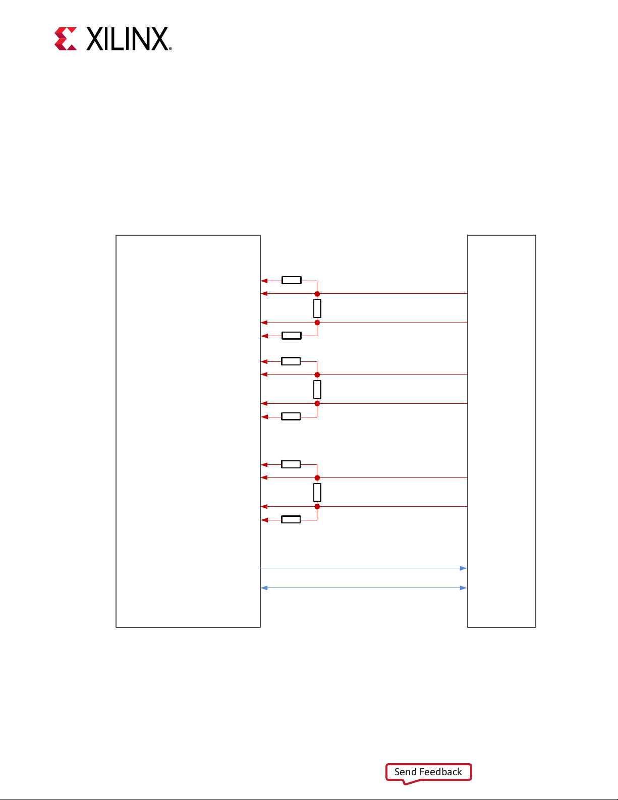
Ethernet PHY Status LEDs
Figure 2, callouts 8, 9
Each Ethernet PHY is connected to a RJ-45 connector with status LEDs integrated into the metal
frame of the connector. The two PHY status LEDs are visible within the frame of each RJ45
Ethernet jack as shown in the following gure. As viewed from the front opening, the le green
LED is the link acvity indicator and the right green LED is the 1000BASE-T link mode indicator.
Figure 11: Ethernet PHY Status LEDs
UG1319 (v1.0) July 12, 2019 www.xilinx.com
SP701 Board User Guide 25
Page 26

Chapter 3: Board Component Descriptions
Send Feedback
For each Ethernet PHY, a separate discrete LED indicates that a link has been established, as
described in the following list:
• PHY1 DP83867IRPAP U14 RJ-45 J9, link established DS2, near item 25 in Figure 2.
• PHY2 DP83867IRPAP U16 RJ-45 J11, link established D2, near item 9 in Figure 2.
Details about the Tri-Mode Ethernet MAC core are provided in the Tri-Mode Ethernet MAC
LogiCORE IP Product Guide (PG051).
I2C Bus Topology
[Figure 2, callout 17]
The SP701 evaluaon board I2C bus implementaon consists of bus I2C0, shared by the FPGA
U1 HP bank 16 and the MSP430 system controller U25. The I2C bus is routed to a TCA9548A 1to-8 bus switch U23 (address 0x74). Seven of the eight bus switch channels are used. The bus
switch can operate at speeds up to 400 kHz.
The SP701 evaluaon board I2C bus topology is shown in the following gure.
Figure 12: SP701 I2C Topology
Spartan-7
FPGA
I2C0_SDA
I2C0_SCL
I2C2_SDA
I2C2_SCL
I2C3_SDA
I2C3_SCL
I2C4_SDA
I2C4_SCL
MSP430
8Ch I2C
Switch
TCA9548APWR
MIPI CSI Conn
MIPI DSI Conn
ADV7511
I2C_MSP430_SDA/SCL
I2C01_SCL/SDA
I2C02_SCL/SDA
I2C03_SCL/SDA
I2C04_SCL/SDA
I2C05_SCL/SDA
I2C06_SCL/SDA
I2C07_SCL/SDA
IO Expander
PGOOD Mon
EEPROM
SysCLK OSC
Si570
Power Monitor
(INA226)-12V
Power Monitor
(INA226)-1V
Test Point for SYS Mon
MP5470 PMIC
FMC-LPC
X22794-050319
UG1319 (v1.0) July 12, 2019 www.xilinx.com
SP701 Board User Guide 26
The following table lists the XC7S100 U1 FPGA I2C bus connecvity.
Page 27

Table 9: XC7S100 U1 FPGA I2C Bus Connectivity
Send Feedback
Chapter 3: Board Component Descriptions
I2C0 Bus
TCA9548 8-Chan. Switch U23 N/A
I2C01_EEPROM_SDA/SCL 0
I2C02_SYSOSC_SDA/SCL 1
I2C03_12VMON_SDA/SCL 2
I2C04_1VMON_SDA/SCL 3
I2C05_SYSMON_SDA/SCL 4 N/A N/A TP10/TP11 TEST POINT
I2C06_MP5470_SDA/SCL 5
I2C07_FMC_SDA/SCL 6
NOT USED 7 N/A N/A N/A
I2C2_CAM_SDA/SCL U1.AE13/AD13
I2C3_DSI_SDA/SCL U1.AB24/AC26
I2C4_HDMI_SDA/SCL U1.K23/J24
TCA6416 Dual 8-bit I/O Port
U24
I2C Switch
Position
MSP430 U25 PORT P4_1, P4_2 I2C_MSP430_SDA/SCL Bus
N/A
Binary Format Hex Format
0b1110100 0x74
0b1010000 0x50
0b1010101 0x55
0b1000001 0X41
0b1000100 0x44
0b1101000 0x68
0b1010000 0x50
XC7S100 FPGA U1 BANK 33 I2C Port
0b1101000 0x78
XC7S100 FPGA U1 BANK 13 I2C Port
XC7S100 FPGA U1 BANK 15 I2C Port
0b1100010 0x72
0b0100000 0x40
I2C Address
0bTBD 0xTBD
Target Device
U23 TCA9548A
U27 M24C32
U45 SI570
U32 INA226
U33 INA226
U34 MP5470GL PMIC
J21 FMC LPC
J8 MIPI-CSI
J20 MIPI-DSI
U18 ADV7511 HDMI
U24 TCA6416A
The MSP430 system controller U25 has a local I2C_MSP430_SDA/SCL bus connected to a dual
8-bit port TI TCA6416A I/O expander U24 (address 0x40). The I/O expander is used for control
outputs and status inputs as listed in the following table.
Table 10: MSP430 TCA6416A U24 I/O Expander Connections
TCA6416A U24 I/O Expander Addr. 0b0100000, 0x40
Port # Schematic Net Name DIR Connected Device
P00 EN_1V35 IN U35 MPM3620A VCCO_1V35 regulator
P01 EN_1V1_ETH IN U38 MPM3805G 1V1_VDD regulator
P02 EN_5V IN U36 MPM3606A 5V regulator
P03 EN_3V3_EXT IN U39 MP8756G 3V3_EXT regulator
P04 EN_VADJ OUT U40 MP8756G VADJ regulator
P05 EN_1V_1V8_2V5_3V3 IN U34 MP5470G VCCINT_1V, VCCO_1V8, VCCO_2V5,
P06 VSEL0_VADJ OUT Q17 FB_VADJ_VSEL0 U40 MP8756G VADJ regulator
P07 VSEL1_VADJ OUT Q18 FB_VADJ_VSEL1 U40 MP8756G VADJ regulator
P10 12VCURSNS_ALERT IN U32 INA226 POWER MONITOR ON INPUT 12V
VCCO_3V3 multi-output regulator
feedback adjusting switch
feedback adjusting switch
UG1319 (v1.0) July 12, 2019 www.xilinx.com
SP701 Board User Guide 27
Page 28

Chapter 3: Board Component Descriptions
Send Feedback
Table 10: MSP430 TCA6416A U24 I/O Expander Connections (cont'd)
TCA6416A U24 I/O Expander Addr. 0b0100000, 0x40
Port # Schematic Net Name DIR Connected Device
P11 1VCURSNS_ALERT IN U33 INA226 POWER MONITOR ON VCCINT_1V
P12 NOT USED IN N/A
P13 M0_0 IN U1 FPGA CONFIG. BANK 0 MODE M0
P14 M1_0 IN U1 FPGA CONFIG. BANK 0 MODE M1
P15 M2_0 IN U1 FPGA CONFIG. BANK 0 MODE M2
P16 FMC_PRSNT_M2C_LT IN J21 FMC LPC
P17 PGOOD_VADJ IN U40 MP8756G VADJ regulator
The TI TCA9548 and TCA6416 data sheets are on the Texas Instruments website. The detailed
FPGA connecons for the feature described in this secon are documented in the SP701 board
XDC le, referenced in Appendix B: Xilinx Design Constraints
HDMI Video Output
[Figure 2, callout 12]
The SP701 board provides a HDMI video output using the Analog Devices ADV7511KSTZ-P
HDMI transmier (U18). The HDMI output is provided on a Molex 47151-1001 HDMI type-A
connector (J13). The ADV7511 is wired to support 1080P 60 Hz, YCbCr 4:2:2 encoding using
24-bit input data mapping.
The SP701 board supports the following HDMI device interfaces:
• 24 data lines
• Independent VSYNC, HSYNC
• Single-ended input CLK
• Interrupt Out Pin to FPGA
• I2C
• SPDIF
The HDMI output interface is shown in the following gure.
UG1319 (v1.0) July 12, 2019 www.xilinx.com
SP701 Board User Guide 28
Page 29

Chapter 3: Board Component Descriptions
Send Feedback
Figure 13: HDMI Output Interface
Spartan-7 FPGA
(Master)
HDMI_R_D[23:0]
30E
30E
HDMI_D[23:0]
HDMI_HSYNC
HDMI_VSYNC
HDMI_CLK
HDMI_INT
HDMI_DE
HDMI_SPDIF
I2C_SCL_HDMI
I2C_SDA_HDMI
1.8V for Digital/IO
1.8V for Digital PLL
D[23:8]
HSYNC
VSYNC
CLK
INT
DE
SPDIF
ADV7511
HDMI Transmitter
SCL
SDA
DVDD
PVDD
R_EXT
887E
D[35:24],D[7:0]
Tx0_P/N
Tx1_P/N
Tx2_P/N
TxC_P/N
DDC_SCL
DDC_SDA
HEAC_P
HEAC_N
HPD
AVDD
PLVDD
BGVDD
MVDD
CEC_CLK
CEC
HDMI_CEC_CLK
HDMIOUT_D0_P/N
HDMIOUT_D1_P/N
HDMIOUT_D2_P/N
HDMIOUT_CLK_P/N
I2C_SCL_HDMIDDC
I2C_SDA_HDMIDDC
50E
1.8V
50E
HDMI_CEC
1.8V for TMDS Output
1.8V for Analog PLL
1.8V
3.3V
HDMI_HEAC_P
HDMI_HEAC_N
2.5V
25E
TMDS_D0_+/ -
TMDS_D1_+/ -
TMDS_D2_+/ -
TMDS_C_+/ -
SCL
SDA
HEAC+
HEAC-
CEC
X22795-052919
For more details, see the ADV7511KSTZ-P data sheet at the Analog Devices website. The
detailed FPGA connecons for the feature described in this secon are documented in the
SP701 board XDC le, referenced in Appendix B: Xilinx Design Constraints.
SIT8102
12 MHz
50ppm
HDMI Conn
MIPI-CSI and MIPI-DSI
[Figure 2, callout 10, 11]
The mobile industry processor interface (MIPI) is a serial communicaon interface specicaon
promoted by the MIPI Alliance. An FPGA MIPI implementaon provides a standard connecon
medium for cameras and displays referred to as a camera serial interface (CSI) or a display serial
interface (DSI). Both interface standards use the PHY specicaon known as D-PHY. The D-PHY
specicaon provides a exible, low-cost, high-speed serial interface soluon for communicaon
interconnecon between components inside mobile devices.
FPGAs do not have I/O standards that can navely support D-PHY. Connecng MINI-equipped
camera and display components requires implemenng the D-PHY hardware specicaon with
discrete components outside the FPGA.
See the D-PHY Soluons (XAPP894) applicaon note for more informaon about:
• MIPI-CSI (input) scalable low-voltage signaling (SLVS) condioning to FPGA LVDS25.
• MIPI-DSI (output) FPGA dierenal HSTL18 condioning to SLVS.
UG1319 (v1.0) July 12, 2019 www.xilinx.com
SP701 Board User Guide 29
Page 30
Chapter 3: Board Component Descriptions
Send Feedback
The detailed FPGA connecons for the feature described in this secon are documented in the
SP701 board XDC le, referenced in Appendix B: Xilinx Design Constraints.
MIPI-CSI
The SP701 board supports MIPI-CSI. The Digilent PCAM module has been tested with this
board. MIPI-CSI interface is connected to AMP/TE Connecvity 1-1734248-5 15-pin connector
J8. MIPI-CSI interface is shown in the following gure.
Figure 14: MIPI-CSI Interface
CSI_LP0_P
CSI_D0_P
CSI_D0_N
CSI_LP0_N
CSI_LP1_P
CSI_D1_P
CSI_D1_N
CSI_LP1_N
Spartan-7 FPGA
(Slave)
CSI_LP_CLK_P
CSI_CLK_P
CSI_CLK_N
CSI_LP_CLK_N
100E
100E
100E
100E
100E
100E
150E
150E
150E
CSI_D0_P
CSI_D0_N
CSI_D1_P
CSI_D1_N
Camera
Interface
Connector
(Master)
CSI_CLK_P
CSI_CLK_N
I2C2_SCL
UG1319 (v1.0) July 12, 2019 www.xilinx.com
SP701 Board User Guide 30
I2C2_SDA
X22796-050319
See the Digilent website for informaon about Pcam 5.
Page 31

Chapter 3: Board Component Descriptions
Send Feedback
MIPI-DSI
The SP701 board provides MIPI DSI (display serial interface) support. The MIPI-DSI interface is
connected to Hirose FH34SJ-34S-0.5SH 34-pin connector J20. The MIPI-DSI interface is shown
in the following gure.
Figure 15: MIPI-DSI Interface
DSI_LP0_P
60E
DSI_D0_P
DSI_D0_N
DSI_LP0_N
150E
150E
60E
120E
120E
DSI_D0_P
DSI_D0_N
DSI_D1_P
DSI_D1_N
Spartan-7 FPGA
(Master)
DSI_LP3_P
DSI_D3_P
DSI_D3_N
DSI_LP3_N
DSI_LP_CLK_P
DSI_CLK_P
DSI_CLK_N
DSI_LP_CLK_N
150E
150E
150E
150E
60E
60E
60E
60E
120E
120E
120E
120E
DSI_D2_P
DSI_D2_N
DSI_D3_P
DSI_D3_N
DSI_CLK_P
DSI_CLK_N
I2C3_SCL
I2C3_SDA
Display
Interface
Connector
(Slave)
UG1319 (v1.0) July 12, 2019 www.xilinx.com
SP701 Board User Guide 31
X22797-050319
For more informaon about MIPI, see the MIPI Alliance website.
Page 32

Chapter 3: Board Component Descriptions
Send Feedback
Power and Status LEDs
[Figure 2, callout 20]
The following table lists the SP701 power, user, and status LEDs.
Table 11: SP701 Power, User, and Status LEDs
Reference Designator Description (Green Unless Otherwise Noted)
DS1 DONE (blue)
D4 MSP430_LED0
D5 MSP430_LED1
D6 GPIO_LED0
D7 GPIO_LED1
D8 GPIO_LED2
D9 GPIO_LED3
D10 GPIO_LED4
D11 GPIO_LED5
D12 GPIO_LED6
D13 GPIO_LED7
D14 12V On (red)
DS2 ETH1_LED1
D2 ETH2_LED1
User I/O
[Figure 2, callout 20]
The SP701 board provides these user and general purpose I/O capabilies:
• Eight user LEDs, acve-High (callout 20)
○ GPIO_LED[0:7]: D6, D7, D8, D9, D10, D11, D12, D13
• 2x 8-posion user DIP switch, acve-High (callout 23)
○ GPIO_DIP_SW_B[0:7]: SW12
○ GPIO_DIP_SW_B[8:16]: SW10
• Five user PB (geographical) and CPU reset PB, acve-High (callouts 21 and 22)
○ GPIO_SW_[NWCES]: SW4, SW5, SW6, SW7, SW9
○ CPU_RESET: SW8
UG1319 (v1.0) July 12, 2019 www.xilinx.com
SP701 Board User Guide 32
Page 33

Chapter 3: Board Component Descriptions
Send Feedback
Figure 16: User GPIO
Bank 15
Vcco = 3.3V
Bank 13
Vcco = 1.8V
Spartan-7 FPGA
GPIOx8
GPIOx8
GPIOx8
GPIOx5
GPIOx1
1.8V
1.8V
1.8V
1.8V
8X LED
8-pole
8-pole
5x Pushbutton
CPU_RESET
1x Pushbutton
(Green)
DIP SW
DIP SW
N,W,C,E,S
(active-High)
(active-High)
X22798-050319
The detailed FPGA connecons for the feature described in this secon are documented in the
SP701 board XDC le, referenced in Appendix B: Xilinx Design Constraints.
User PMOD GPIO Connectors
[Figure 2, callout 20, 21]
The SP701 evaluaon board implements six right-angle PMOD GPIO receptacles J14-J19. The
3.3V PMOD nets are wired to the XC7S100 FPGA 3.3V bank 16. For more informaon about
PMOD connector compable PMOD modules, see the Digilent Inc. website.
The following gure shows the GPIO PMOD connectors.
UG1319 (v1.0) July 12, 2019 www.xilinx.com
SP701 Board User Guide 33
Page 34

Chapter 3: Board Component Descriptions
Send Feedback
Figure 17: 6x PMOD RA Receptacles
3.3V
GPIO x8
3.3V
GPIO x8
3.3V
GPIO x8
3.3V
GND
GND
GND
Conn
12pin Pmod
Conn
12pin Pmod
Conn
12pin Pmod
Spartan-7 FPGA
(Master)
GPIO x8
GPIO x8
GPIO x8
3.3V
3.3V
GND
GND
GND
Conn
12pin Pmod
Conn
12pin Pmod
Conn
12pin Pmod
X22799-050319
The detailed FPGA connecons for the feature described in this secon are documented in the
SP701 board XDC le, referenced in Appendix B: Xilinx Design Constraints.
UG1319 (v1.0) July 12, 2019 www.xilinx.com
SP701 Board User Guide 34
Page 35

Chapter 3: Board Component Descriptions
Send Feedback
System Controller MSP430
[Figure 2, callout 14]
The SP701 evaluaon board implements an on-board system controller (MSP430F5342 U25)
accessible from the FT4232H USB-UART BCBUS Port D.
Figure 18: MSP430 Block Diagram
USB
x8
x8
x2
USB Conn
Power Supply
Control
Power
Monitoring
Board ID
X22800-051019
Spartan-7
FPGA
4x GPIOs
I2C0
MSP430
System
Controller
32 kHz Crystal
32.7680K
I2C Switch
TCA9548
UART_D
I2C_MSP430
x5
x2
FT4232H
I/O Expander
TCA6416A
5 Pos DIP Switch
2x LED
JTAG Header
for MSP430
I2C01 to I2C08
A host PC resident system controller user interface (SCUI) is provided on the SP701 website. This
GUI enables you to query and control select programmable features such as clocks, FMC
funconality, and power systems parameters. The SP701 documentaon also includes a tutorial
on the SCUI, SP701 System Controller Tutorial (XTP551), and a SP701 Soware Install and Board
Setup Tutorial (XTP552). The instrucons are summarized as follows.
UG1319 (v1.0) July 12, 2019 www.xilinx.com
SP701 Board User Guide 35
1. Ensure that the Silicon Labs VCP USB-UART drivers are installed. See Silicon Labs CP210x
USB-to-UART Installaon Guide (UG1033).
2. Download the SCUI host PC applicaon.
3. Connect a USB cable between your PC and the SP701 USB micro-AB connector (J5).
4. Power-cycle the SP701.
5. Ensure that SYSCTLR LED0 (D4) blinks and LED1 D5 is illuminated.
6. Launch the SCUI.
The SCUI GUI is shown in the following gure.
Page 36

Chapter 3: Board Component Descriptions
Send Feedback
Figure 19: SCUI Graphical User Interface
On the rst use of the SCUI, go to the FMC → Set VADJ → Boot-up tab and click USE FMC
EEPROM Voltage. The SCUI buons are grayed out during command execuon and return to
their original appearance when ready to accept a new command. See the SP701 System
Controller Tutorial (XTP551) and the SP701 Soware Install and Board Setup Tutorial (XTP552)
for more informaon on installing and using the System Controller ulity.
For more details, see the MSP430F5342 data sheet on the Texas Instruments website. The
detailed FPGA connecons for the feature described in this secon are documented in the
SP701 board XDC le, referenced in Appendix B: Xilinx Design Constraints.
FPGA Mezzanine Card Interface
[Figure 2, callout 7]
The SP701 evaluaon board supports the VITA 57.1 FPGA mezzanine card (FMC) specicaon
by providing a low pin count (LPC) FMC connector at J21. LPC connectors use a 10 x 40 form
factor that is parally populated with 160 pins. The connector is keyed so that a mezzanine card,
when installed in the FMC LPC connector on the SP701 evaluaon board, faces away from the
board. The FMC LPC connector pinout is shown in the Appendix A: VITA 57.1 FMC Connector
Pinouts.
UG1319 (v1.0) July 12, 2019 www.xilinx.com
SP701 Board User Guide 36
FMC LPC Connector J21
[Figure 2, callout 7]
The 160-pin connector J21 implements paral FMC LPC connecvity (refer to schemac
0381874 and the XDC le for details).
Page 37

Chapter 3: Board Component Descriptions
Send Feedback
• 68 single-ended, or 34 dierenal user-dened pairs (34 LA pairs: LA[00:33])
• 2 dierenal user clocks
• 2 I2C
• 5 JTAG
• 2 state ags
• 61 ground and 10 power connecons
The SP701 board FMC VADJ voltage for LPC connector J21 is determined by the MSP430
system controller adjusng the Monolithic Power Systems MP8756GD U40 voltage regulator as
described in Board Power System. Valid values for the VADJ_FMC rail are 1.8V, 2.5V, and 3.3V.
The detailed FPGA connecons for the feature described in this secon are documented in the
SP701 board XDC le, referenced in Appendix B: Xilinx Design Constraints.
Power On/Off Slide Switch
[Figure 2, callout 28]
The SP701 board power switch is SW11. Sliding the switch actuator from the o to the on
posion applies 12V power from J30, a 6-pin mini-t connector. Red LED D14 illuminates when
the SP701 board power is on. See Board Power System for details on the on-board power
system.
CAUTION!
The ATX 6-pin connector has a dierent pin-out than J30. Connecng an ATX 6-pin connector into J30 damages
the SP701 board and voids the board warranty.
The following
Do NOT plug a PC ATX power supply 6-pin connector into the SP701 board power connector J30.
gure shows the power connector J30, power switch SW11, and LED indicator
D14.
UG1319 (v1.0) July 12, 2019 www.xilinx.com
SP701 Board User Guide 37
Page 38

Chapter 3: Board Component Descriptions
Send Feedback
Figure 20: SP701 Power Input
Board Power System
[Figure 2, callout 29]
The SP701 power system is comprised of monolithic power systems components. The four
outputs (VCCINT, VCCO_1V8, VCCO_2V5, and VCCO_3V3) of the MP5470 U34 regulator are
adjustable through its I2C bus connecon accessible from the FPGA U1 Bank 16 and the
MSP430 system controller.
The following gure shows the SP701 power system block diagram.
UG1319 (v1.0) July 12, 2019 www.xilinx.com
SP701 Board User Guide 38
Page 39
1
Send Feedback
4
2
5
3
6
12V External
Connector
39-30-1060
Power
Noise Filter
Chapter 3: Board Component Descriptions
Figure 21: Power System Block Diagram
Current
Monitor
12V
12.6V
0.65A
0.8A
0.08A
0.08A
2A
1A
1.1A
0.04A
VIN1
MP5470
Input : 4V-16
Output : 0.55V-5.46V
3A/3A/2A/2A Buck
VIN2
MPM3620A
Input: 4.5V-24V
2A Buck
MPM3606A
Input: 4.5V-21V
0.6A Buck
MP8756
Input: 4.5V-26V
6A Buck
MP8756
Input: 4.5V-26V
6A Buck
MPM3620A
Input: 4.5V-26V
2A Buck
3A
3A
2A
2A
Current Monitor
6A
1V @ 2.5A
1.8V @ 2A
2.5 @ 1A
3.3V @ 1.5A
1.35V @ 0.6A
MP20073
Input: 1.3V-6V
2A VTT-LDO
5V @ 0.15A
2A
3.3V @ 0.1A
3.3V AUX for FMC
MPM3805
Input: 2.5V-6B
0.6A Buck
6A
1.6A
1V
1.05V
1.8V
1.89V
2.5V
2.625V
3.3V
3.465V
1.35V
1.43V
0.675V
5V
5.25V
3.3V
3A
3.465V
3.3V
3.465V
3A
12V
1A
12.6V
VADJ
1.8V to 3.465V
3.3V
3.465V
1.1V
FPGA VCCINT
FPGA, 2x DP83867,
ADV7511, UI
FPGA VCCIO, 2x
DP83867 IO
FPGA, FLASH,
EEPROM, FT4232, UI
& 6xPmod
FPGA & DRAM
VTT_0V675
DDR3L
HDMI Conn
3.3V/3A for MIPI
Display & Camera
FMC-LPC
2x DP83867IR Core
(2x 125mA)
X22801-050319
The following table lists the SP701 power system voltage regulators.
Table 12: SP701 Power System
Device Type
Ref.
Des.
INA226AIDGS U32
MP5470GL U34
INA226AIDGS U33
MPM3620A U35 N/A Synchronous
MPM3606A U36 N/A Synchronous
MPM3805GQB U38 N/A Synchronous
I2C
Address
0x41
0x68
0x44
Description O/P
Current and
power monitor
Four-output
PMIC
Current and
power monitor
step-down
converter
step-down
converter
step-down
converter
N/A 12V N/A N/A 24
SW1 VCCINT_1V 1.00V 3A 24
SW2 VCCO_1V8 1.80V 2A
SW3 VCCO_2V5 2.50V 2A
SW4 VCCO_3V3 3.30V 2A
N/A VCCINT_1V N/A N/A 24
OUT VCCO_1V35 1.35V 2A 25
OUT 5V 5.0V 0.6A 25
OUT 1V1_VDD 1.10V 0.6A 25
Power Rail
Net Name
Voltage
Power
Rail
Max.
Current
Schematic
Page
UG1319 (v1.0) July 12, 2019 www.xilinx.com
SP701 Board User Guide 39
Page 40

Table 12: SP701 Power System (cont'd)
Send Feedback
Chapter 3: Board Component Descriptions
Device Type
MPM3620A U37 N/A Synchronous
MP8756GD U39 N/A POL switching
MP8756GD U40 N/A POL switching
MP20073DH U13 N/A DDR memory
Ref.
Des.
I2C
Address
Description O/P
step-down
converter
regulator
regulator
termination
regulator
Power Rail
Net Name
OUT 3V3AUX 3.30V 2A 25
SW 3V3_EXT 3.30V 6A 26
SW VADJ 1.80V 6A 26
VTTREF VTTREF 0.675V 2A 6
Power
Rail
Voltage
The following gure shows the SP701 power system sequencing diagram.
Figure 22: Power System Sequence
POWER UP SEQUENCE
12V
Max.
Current
Schematic
Page
3V3AUX
SYS CTRL
MSP430
VCCINT_1V VCCO_1V8
VCCO_2V5 VCCO_3V3
VCCO_1V35 1V1_VDD 5V 3V3_EXT VADJ
X22953-061119
The opons for VADJ are 1.8V, 2.5V, and 3.3V. They can be selected using the System Controller
(MSP430) I2C connected TCA64164A I/O expander U24 ports P06 VSEL0_VADJ and P07
VSEL1_VADJ pins. The VADJ regulator can similarly be powered ON/OFF by the TCA64164A
I/O expander U24 port P04 pin.
UG1319 (v1.0) July 12, 2019 www.xilinx.com
SP701 Board User Guide 40
Page 41

Chapter 3: Board Component Descriptions
Send Feedback
Table 13: SP701 Power System VADJ
VADJ VSEL0_VADJ (U24.10) VSEL1_VADJ (24.11)
3.3V 1 1
2.5V 0 1
1.8V 0 0
XADC Header
[Figure 2, callout 34]
The Xilinx® System Monitor (SYSMON) technology enables monitoring the physical environment
via on-chip power supply, temperature sensors, and external analog inputs. SYSMON is a key
part of the power management infrastructure for the board, providing telemetry informaon for
the supplies for the Xilinx device and the various other on-board supplies.
The analog mixed signal (AMS) block present in Xilinx 7 series FPGAs is called XADC (includes
SYSMON funcon). Apart from the SYSMON funcon, the ADCs provide a general-purpose,
high-precision analog interface for a range of applicaons. The following gure shows the block
diagram of the single XADC block available in the Spartan-7 family. The interface can be JTAG,
DRP, and AXI to the XADC/SYSMON block.
See the 7 Series FPGAs and Zynq-7000 SoC XADC Dual 12-Bit 1 MSPS Analog-to-Digital Converter
User Guide (UG480) for details on the capabilies of the analog front end.
UG1319 (v1.0) July 12, 2019 www.xilinx.com
SP701 Board User Guide 41
Page 42

Chapter 3: Board Component Descriptions
Send Feedback
Figure 23: XADC (SYSMON) Block Diagram
External
Analog
Inputs
Temperature
VP_0
VN_0
VAUXP[0]
VAUXN[0]
VAUXP[12]
VAUXN[12]
VAUXP[13]
VAUXN[13]
VAUXP[14]
VAUXN[14]
VAUXP[15]
VAUXN[15]
Temperature
Sensor
Die
°C
Mux
Supply
Sensors
VCCINT
VCCAUX
VCCBRAM
VCCPINT
VCCPAUX
VCCO_DDR
Mux
VREP_0
1 MSPS
VREFN_0
On-Chip Ref
1.25V
12-bit,
ADC A
12-bit,
1 MSPS
ADC B
Control
Registers
64 x 16 bits
Read/Write
JTAG
DRP
FPGA
Interconnect
It is not necessary to instanate the XADC in a design to access the on-chip monitoring
capability. However, if the XADC is not instanated in a design, the only way to access this
informaon is through the JTAG test access port (TAP). To allow access to the status registers
(measurement results) from the FPGA logic, the XADC must be instanated.
Status
Registers
64 x 16 bits
Read Only
X17015-070719
UG1319 (v1.0) July 12, 2019 www.xilinx.com
SP701 Board User Guide 42
The following gure shows the SYSMON implementaon and SYSMON header J24, a 2x10
shrouded male pin header. Jumper J26 is provided to select internal reference or external
reference.
Page 43

Chapter 3: Board Component Descriptions
Send Feedback
Figure 24: XADC (SYSMON) Interface
-
See the SP701 schemac 0381874 for detailed SYSMON header J24 and XADC_VREF opon
details.
X22606-040219
UG1319 (v1.0) July 12, 2019 www.xilinx.com
SP701 Board User Guide 43
Page 44

Appendix A: VITA 57.1 FMC Connector Pinouts
Send Feedback
Appendix A
VITA 57.1 FMC Connector Pinouts
The following gure shows the pinout of the FPGA mezzanine card (FMC) low pin count (LPC)
connector dened by the VITA 57.1 FMC specicaon. For a descripon of how the SP701
evaluaon board implements the FMC specicaon, see FPGA Mezzanine Card Interface and
FMC LPC Connector J21.
Figure 25: FMC LPC Connector Pinout
UG1319 (v1.0) July 12, 2019 www.xilinx.com
SP701 Board User Guide 44
X22605-040219
Page 45

Xilinx Design Constraints
Send Feedback
Overview
The Xilinx design constraints (XDC) le template for the SP701 board provides for designs
targeng the SP701 evaluaon board. Net names in the constraints le correlate with net names
on the latest SP701 evaluaon board schemac. Idenfy the appropriate pins and replace the net
names with net names in the user RTL. See the Vivado Design Suite User Guide: Using Constraints
(UG903) for more informaon.
Appendix B
The FMC LPC connector J21 is connected to FPGA banks powered by the variable voltage V
(1.8V nominal). Because dierent FMC cards implement dierent circuitry, the FMC bank I/O
standards must be uniquely dened by each customer.
IMPORTANT!
See the SP701 board website documentaon tab (Board Files check box) for the XDC le.
ADJ
UG1319 (v1.0) July 12, 2019 www.xilinx.com
SP701 Board User Guide 45
Page 46

Appendix C: Regulatory and Compliance Information
Send Feedback
Regulatory and Compliance
Information
This product is designed and tested to conform to the European Union direcves and standards
described in this secon.
For Technical Support, open a Support Service Request.
Appendix C
CE Information
CE Directives
2006/95/EC, Low Voltage Direcve (LVD)
2004/108/EC, Electromagnec Compability (EMC) Direcve
CE Standards
EN standards are maintained by the European Commiee for Electrotechnical Standardizaon
(CENELEC). IEC standards are maintained by the Internaonal Electrotechnical Commission (IEC).
CE Electromagnetic Compatibility
EN 55022:2010, Informaon Technology Equipment Radio Disturbance Characteriscs – Limits and
Methods of Measurement
EN 55024:2010, Informaon Technology Equipment Immunity Characteriscs – Limits and Methods
of Measurement
This is a Class A product. In a domesc environment, this product can cause radio interference, in
which case the user might be required to take adequate measures.
UG1319 (v1.0) July 12, 2019 www.xilinx.com
SP701 Board User Guide 46
CE Safety
IEC 60950-1:2005, Informaon technology equipment – Safety, Part 1: General requirements
EN 60950-1:2006, Informaon technology equipment – Safety, Part 1: General requirements
Page 47

Compliance Markings
Send Feedback
In August of 2005, the European Union (EU) implemented the EU Waste Electrical
and Electronic Equipment (WEEE) Directive 2002/96/EC and later the WEEE Recast
Directive 2012/19/EU. These directives require Producers of electronic and
electrical equipment (EEE) to manage and finance the collection, reuse, recycling
and to appropriately treat WEEE that the Producer places on the EU market after
August 13, 2005. The goal of this directive is to minimize the volume of electrical
and electronic waste disposal and to encourage re-use and recycling at the end
of life.
Xilinx has met its national obligations to the EU WEEE Directive by registering in
those countries to which Xilinx is an importer. Xilinx has also elected to join WEEE
Compliance Schemes in some countries to help manage customer returns at
end-of-life.
If you have purchased Xilinx-branded electrical or electronic products in the EU
and are intending to discard these products at the end of their useful life, please
do not dispose of them with your other household or municipal waste. Xilinx has
labeled its branded electronic products with the WEEE Symbol to alert our
customers that products bearing this label should not be disposed of in a landfill
or with municipal or household waste in the EU.
Appendix C: Regulatory and Compliance Information
This product complies with Directive 2002/95/EC on the restriction of hazardous
substances (RoHS) in electrical and electronic equipment.
This product complies with CE Directives 2006/95/EC, Low Voltage Directive (LVD)
and 2004/108/EC, Electromagnetic Compatibility (EMC) Directive.
UG1319 (v1.0) July 12, 2019 www.xilinx.com
SP701 Board User Guide 47
Page 48

Appendix D: Additional Resources and Legal Notices
Send Feedback
Appendix D
Additional Resources and Legal
Notices
Xilinx Resources
For support resources such as Answers, Documentaon, Downloads, and Forums, see Xilinx
Support.
Documentation Navigator and Design Hubs
Xilinx® Documentaon Navigator (DocNav) provides access to Xilinx documents, videos, and
support resources, which you can lter and search to nd informaon. To open DocNav:
• From the Vivado® IDE, select Help → Documentaon and Tutorials.
• On Windows, select Start → All Programs → Xilinx Design Tools → DocNav.
• At the Linux command prompt, enter docnav.
Xilinx Design Hubs provide links to documentaon organized by design tasks and other topics,
which you can use to learn key concepts and address frequently asked quesons. To access the
Design Hubs:
• In DocNav, click the Design Hubs View tab.
• On the Xilinx website, see the Design Hubs page.
Note: For more informaon on DocNav, see the Documentaon Navigator page on the Xilinx website.
UG1319 (v1.0) July 12, 2019 www.xilinx.com
SP701 Board User Guide 48
Page 49

References
Send Feedback
The most up to date informaon related to the SP701 board and its documentaon is available
on the following websites.
• SP701 Evaluaon Kit
• SP701 Evaluaon Kit Master Answer Record 72092
These documents provide supplemental material useful with this guide:
1. 7 Series FPGAs Data Sheet: Overview (DS180)
2. Spartan-7 FPGAs Data Sheet: DC and AC Switching Characteriscs (DS189)
3. Zynq-7000 SoC and 7 Series Devices Memory Interface Soluons (UG586)
4. 7 Series FPGAs Memory Resources User Guide (UG473)
5. 7 Series FPGAs Conguraon User Guide (UG470)
Appendix D: Additional Resources and Legal Notices
6. 7 Series FPGAs Packaging and Pinout Product Specicaon (UG475)
7. 7 Series FPGAs and Zynq-7000 SoC XADC Dual 12-Bit 1 MSPS Analog-to-Digital Converter User
Guide (UG480)
8. 7 Series FPGAs PCB Design Guide (UG483)
9. Tri-Mode Ethernet MAC LogiCORE IP Product Guide (PG051)
10. Vivado Design Suite User Guide: Using Constraints (UG903)
11. D-PHY Soluons (XAPP894)
12. SP701 System Controller Tutorial (XTP551)
13. SP701 Soware Install and Board Setup Tutorial (XTP552)
Documents associated with other devices used by the SP701 board are available at these
vendor websites:
14. Micron Technology: www.micron.com (MT25QL01GBBBESF-0SIT,
MT41K256M16TW-107:P)
15. Analog Devices: www.analog.com/en/index (ADV7511KSTZ-P)
16. Samtec: www.samtec.com (SEAF series connectors)
17. VITA FMC Markeng Alliance: www.vita.com/fmc (FPGA Mezzanine Card (FMC) VITA 57.1,
57.4 specicaons)
UG1319 (v1.0) July 12, 2019 www.xilinx.com
SP701 Board User Guide 49
18. Silicon Labs: www.silabs.com (Si570)
19. Texas Instruments: www..com (TCA9548A, TCA6416A, DP83867IRP, ADP123)
20. Future Technology Devices Internaonal Ltd.: www.dichip.com (FT4232HQ)
Page 50

Appendix D: Additional Resources and Legal Notices
Send Feedback
Please Read: Important Legal Notices
The informaon disclosed to you hereunder (the "Materials") is provided solely for the selecon
and use of Xilinx products. To the maximum extent permied by applicable law: (1) Materials are
made available "AS IS" and with all faults, Xilinx hereby DISCLAIMS ALL WARRANTIES AND
CONDITIONS, EXPRESS, IMPLIED, OR STATUTORY, INCLUDING BUT NOT LIMITED TO
WARRANTIES OF MERCHANTABILITY, NON-INFRINGEMENT, OR FITNESS FOR ANY
PARTICULAR PURPOSE; and (2) Xilinx shall not be liable (whether in contract or tort, including
negligence, or under any other theory of liability) for any loss or damage of any kind or nature
related to, arising under, or in connecon with, the Materials (including your use of the
Materials), including for any direct, indirect, special, incidental, or consequenal loss or damage
(including loss of data, prots, goodwill, or any type of loss or damage suered as a result of any
acon brought by a third party) even if such damage or loss was reasonably foreseeable or Xilinx
had been advised of the possibility of the same. Xilinx assumes no obligaon to correct any
errors contained in the Materials or to nofy you of updates to the Materials or to product
specicaons. You may not reproduce, modify, distribute, or publicly display the Materials
without prior wrien consent. Certain products are subject to the terms and condions of
Xilinx's limited warranty, please refer to Xilinx's Terms of Sale which can be viewed at hps://
www.xilinx.com/legal.htm#tos; IP cores may be subject to warranty and support terms contained
in a license issued to you by Xilinx. Xilinx products are not designed or intended to be fail-safe or
for use in any applicaon requiring fail-safe performance; you assume sole risk and liability for
use of Xilinx products in such crical applicaons, please refer to Xilinx's Terms of Sale which can
be viewed at hps://www.xilinx.com/legal.htm#tos.
AUTOMOTIVE APPLICATIONS DISCLAIMER
AUTOMOTIVE PRODUCTS (IDENTIFIED AS "XA" IN THE PART NUMBER) ARE NOT
WARRANTED FOR USE IN THE DEPLOYMENT OF AIRBAGS OR FOR USE IN APPLICATIONS
THAT AFFECT CONTROL OF A VEHICLE ("SAFETY APPLICATION") UNLESS THERE IS A
SAFETY CONCEPT OR REDUNDANCY FEATURE CONSISTENT WITH THE ISO 26262
AUTOMOTIVE SAFETY STANDARD ("SAFETY DESIGN"). CUSTOMER SHALL, PRIOR TO USING
OR DISTRIBUTING ANY SYSTEMS THAT INCORPORATE PRODUCTS, THOROUGHLY TEST
SUCH SYSTEMS FOR SAFETY PURPOSES. USE OF PRODUCTS IN A SAFETY APPLICATION
WITHOUT A SAFETY DESIGN IS FULLY AT THE RISK OF CUSTOMER, SUBJECT ONLY TO
APPLICABLE LAWS AND REGULATIONS GOVERNING LIMITATIONS ON PRODUCT
LIABILITY.
Copyright
© Copyright 2019 Xilinx, Inc. Xilinx, the Xilinx logo, Alveo, Arx, Kintex, Spartan, Versal, Virtex,
Vivado, Zynq, and other designated brands included herein are trademarks of Xilinx in the United
States and other countries. All other trademarks are the property of their respecve owners.
UG1319 (v1.0) July 12, 2019 www.xilinx.com
SP701 Board User Guide 50
 Loading...