

Page 1

SP605 Hardware
User Guide
UG526 (v1.8) September 24, 2012
Page 2
© Copyright 2009–2012 Xilinx, Inc. Xilinx, the Xilinx logo, Artix, ISE, Kintex, Spartan, Virtex, Zynq, and other designated brands included
herein are trademarks of Xilinx in the United States and other countries. All other trademarks are the property of their respective owners.
DISCLAIMER
The information disclosed to you hereunder (the “Materials”) is provided solely for the selection and use of Xilinx products. To the maximum
extent permitted by applicable law: (1) Materials are made available “AS IS” and with all faults, Xilinx hereby DISCLAIMS ALL
WARRANTIES AND CONDITIONS, EXPRESS, IMPLIED, OR STATUTORY, INCLUDING BUT NOT LIMITED TO WARRANTIES OF
MERCHANTABILITY, NON-INFRINGEMENT, OR FITNESS FOR ANY PARTICULAR PURPOSE; and (2) Xilinx shall not be liable (whether
in contract or tort, including negligence, or under any other theory of liability) for any loss or damage of any kind or nature related to, arising
under, or in connection with, the Materials (including your use of the Materials), including for any direct, indirect, special, incidental, or
consequential loss or damage (including loss of data, profits, goodwill, or any type of loss or damage suffered as a result of any action
brought by a third party) even if such damage or loss was reasonably foreseeable or Xilinx had been advised of the possibility of the same.
Xilinx assumes no obligation to correct any errors contained in the Materials, or to advise you of any corrections or update. You may not
reproduce, modify, distribute, or publicly display the Materials without prior written consent. Certain products are subject to the terms and
conditions of the Limited Warranties which can be viewed at http://www.xilinx.com/warranty.htm
support terms contained in a license issued to you by Xilinx. Xilinx products are not designed or intended to be fail-safe or for use in any
application requiring fail-safe performance; you assume sole risk and liability for use of Xilinx products in Critical Applications:
http://www.xilinx.com/warranty.htm#critapps
.
; IP cores may be subject to warranty and
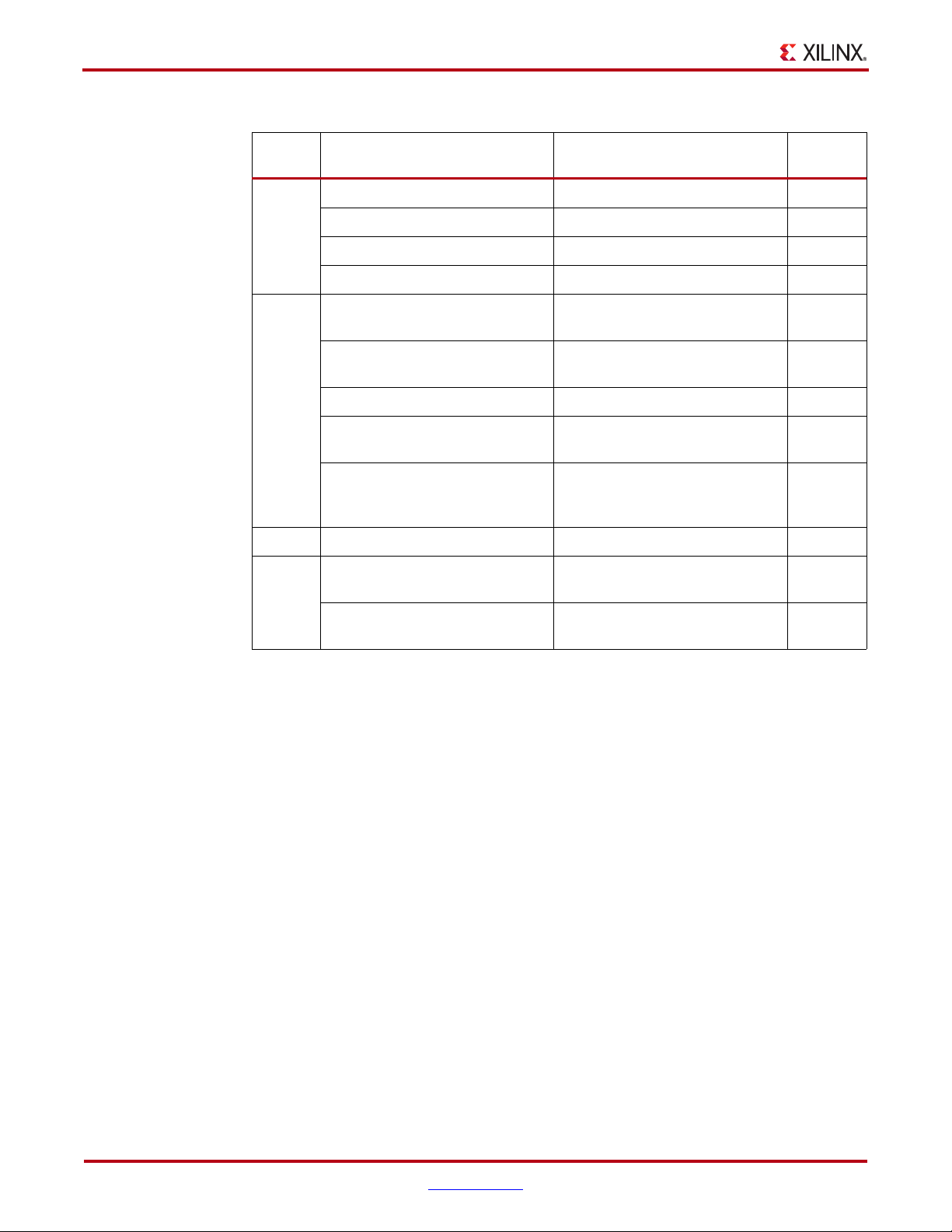
Revision History
The following table shows the revision history for this document.
Date Version Revision
10/07/09 1.0 Initial Xilinx release.
11/09/09 1.1 • Updated Figure 1-17 and Figure 1-23.
• Changed speed grade from -2 to -3.
• Miscellaneous typographical edits.
02/01/10 1.1.1 Minor typographical edits to Ta bl e 1 -2 4 and Ta b le 1 -2 5.
05/18/10 1.2 Updated Figure 1-2. Added Note 6 to Ta bl e 1-11 . Updated board connections for
SFP_TX_DISABLE in Tab le 1 -12. Added note about FMC LPC J63 connector in 18. VITA
57.1 FMC LPC Connector. Updated U1 FPGA Pin column for FMC_LA00_CC_P/N in
Ta bl e 1- 2 8. Updated description of PMBus Pod and TI Fusion Digital Power Software
GUI in Onboard Power Regulation. Updated Appendix C, VITA 57.1 FMC LPC
Connector Pinout, and Appendix D, SP605 Master UCF.
06/16/10 1.3 Updated 2. 128 MB DDR3 Component Memory. Added note 1 to Ta bl e 1- 30 .
09/24/10 1.4 Updated description of Fusion Digital Power Software in Onboard Power Regulation.
02/16/11 1.5 Revised oscillator manufacturer information from Epson to SiTime in Ta bl e 1-1 . Revised
oscillator manufacturer information from Epson to SiTime on page page 26. Deleted note
on page 44 referring to J55: “Note: This header is not installed on the SP605 as built.”
Revised values for R50 and R216 in Figure 1-12. Revised oscillator manufacturer
information from Epson to SiTime on page page 61.
07/18/11 1.6 Corrected “jitter” to “stability” in section Oscillator (Differential), page 26. Revised the
feature and notes descriptions for reference numbers 6 and 12 in Ta b le 1-1, p age 12 .
Revised FPGA pin numbers for ZIO and RZQ in Tab l e 1-4, page 1 7. Added Table 1-29,
page 55, Table 1-31, page 58, and table notes in Tab l e 1- 30 .
06/19/12 1.7 Removed reference to FPGA speed grade in 2. 128 MB DDR3 Component Memory,
page 16. Added IIC External Access Header, page 39. Updated SFP Module connector
reference designator in 8. Multi-Gigabit Transceivers (GTP MGTs), page 28.
SP605 Hardware User Guide www.xilinx.com UG526 (v1.8) September 24, 2012
Page 3

Date Version Revision
09/24/12 1.8 Updated Figure 1-2, page 12. Added Regulatory and Compliance Information, page 73.
UG526 (v1.8) September 24, 2012 www.xilinx.com SP605 Hardware User Guide
Page 4

SP605 Hardware User Guide www.xilinx.com UG526 (v1.8) September 24, 2012
Page 5

Table of Contents
Revision History . . . . . . . . . . . . . . . . . . . . . . . . . . . . . . . . . . . . . . . . . . . . . . . . . . . . . . . . . . . . . 2
Preface: About This Guide
Guide Contents . . . . . . . . . . . . . . . . . . . . . . . . . . . . . . . . . . . . . . . . . . . . . . . . . . . . . . . . . . . . . . 7
Additional Documentation . . . . . . . . . . . . . . . . . . . . . . . . . . . . . . . . . . . . . . . . . . . . . . . . . . . 7
Additional Support Resources. . . . . . . . . . . . . . . . . . . . . . . . . . . . . . . . . . . . . . . . . . . . . . . . 8
Chapter 1: SP605 Evaluation Board
Overview . . . . . . . . . . . . . . . . . . . . . . . . . . . . . . . . . . . . . . . . . . . . . . . . . . . . . . . . . . . . . . . . . . . . 9
Additional Information . . . . . . . . . . . . . . . . . . . . . . . . . . . . . . . . . . . . . . . . . . . . . . . . . . . . . 9
Features . . . . . . . . . . . . . . . . . . . . . . . . . . . . . . . . . . . . . . . . . . . . . . . . . . . . . . . . . . . . . . . . . 10
Block Diagram . . . . . . . . . . . . . . . . . . . . . . . . . . . . . . . . . . . . . . . . . . . . . . . . . . . . . . . . . . . 11
Related Xilinx Documents. . . . . . . . . . . . . . . . . . . . . . . . . . . . . . . . . . . . . . . . . . . . . . . . . . . 12
Detailed Description . . . . . . . . . . . . . . . . . . . . . . . . . . . . . . . . . . . . . . . . . . . . . . . . . . . . . . . . 12
1. Spartan-6 XC6SLX45T-3FGG484 FPGA . . . . . . . . . . . . . . . . . . . . . . . . . . . . . . . . . . . . 14
Configuration . . . . . . . . . . . . . . . . . . . . . . . . . . . . . . . . . . . . . . . . . . . . . . . . . . . . . . . . . 14
I/O Voltage Rails . . . . . . . . . . . . . . . . . . . . . . . . . . . . . . . . . . . . . . . . . . . . . . . . . . . . . . 16
2. 128 MB DDR3 Component Memory . . . . . . . . . . . . . . . . . . . . . . . . . . . . . . . . . . . . . . . 16
3. SPI x4 Flash . . . . . . . . . . . . . . . . . . . . . . . . . . . . . . . . . . . . . . . . . . . . . . . . . . . . . . . . . . . . 19
4. Linear BPI Flash . . . . . . . . . . . . . . . . . . . . . . . . . . . . . . . . . . . . . . . . . . . . . . . . . . . . . . . . 21
FPGA Design Considerations for the Configuration Flash . . . . . . . . . . . . . . . . . . . . . . . 23
5. System ACE CF and CompactFlash Connector. . . . . . . . . . . . . . . . . . . . . . . . . . . . . . 23
6. USB JTAG . . . . . . . . . . . . . . . . . . . . . . . . . . . . . . . . . . . . . . . . . . . . . . . . . . . . . . . . . . . . . 25
7. Clock Generation . . . . . . . . . . . . . . . . . . . . . . . . . . . . . . . . . . . . . . . . . . . . . . . . . . . . . . . 26
Oscillator (Differential) . . . . . . . . . . . . . . . . . . . . . . . . . . . . . . . . . . . . . . . . . . . . . . . . . . 26
Oscillator Socket (Single-Ended, 2.5V or 3.3V) . . . . . . . . . . . . . . . . . . . . . . . . . . . . . . . . 27
SMA Connectors (Differential) . . . . . . . . . . . . . . . . . . . . . . . . . . . . . . . . . . . . . . . . . . . . 28
8. Multi-Gigabit Transceivers (GTP MGTs) . . . . . . . . . . . . . . . . . . . . . . . . . . . . . . . . . . . 28
9. PCI Express Endpoint Connectivity . . . . . . . . . . . . . . . . . . . . . . . . . . . . . . . . . . . . . . . 31
10. SFP Module Connector . . . . . . . . . . . . . . . . . . . . . . . . . . . . . . . . . . . . . . . . . . . . . . . . . 33
11. 10/100/1000 Tri-Speed Ethernet PHY . . . . . . . . . . . . . . . . . . . . . . . . . . . . . . . . . . . . 34
12. USB-to-UART Bridge. . . . . . . . . . . . . . . . . . . . . . . . . . . . . . . . . . . . . . . . . . . . . . . . . . . 36
13. DVI CODEC . . . . . . . . . . . . . . . . . . . . . . . . . . . . . . . . . . . . . . . . . . . . . . . . . . . . . . . . . . 37
14. IIC Bus . . . . . . . . . . . . . . . . . . . . . . . . . . . . . . . . . . . . . . . . . . . . . . . . . . . . . . . . . . . . . . . 38
IIC External Access Header . . . . . . . . . . . . . . . . . . . . . . . . . . . . . . . . . . . . . . . . . . . . . . 39
8-Kb NV Memory . . . . . . . . . . . . . . . . . . . . . . . . . . . . . . . . . . . . . . . . . . . . . . . . . . . . . . 39
15. Status LEDs . . . . . . . . . . . . . . . . . . . . . . . . . . . . . . . . . . . . . . . . . . . . . . . . . . . . . . . . . . . 41
Ethernet PHY Status LEDs . . . . . . . . . . . . . . . . . . . . . . . . . . . . . . . . . . . . . . . . . . . . . . . 42
FPGA INIT and DONE LEDs . . . . . . . . . . . . . . . . . . . . . . . . . . . . . . . . . . . . . . . . . . . . . 43
16. User I/O . . . . . . . . . . . . . . . . . . . . . . . . . . . . . . . . . . . . . . . . . . . . . . . . . . . . . . . . . . . . . 44
User LEDs . . . . . . . . . . . . . . . . . . . . . . . . . . . . . . . . . . . . . . . . . . . . . . . . . . . . . . . . . . . . 44
User Pushbutton Switches . . . . . . . . . . . . . . . . . . . . . . . . . . . . . . . . . . . . . . . . . . . . . . . 45
User DIP Switch . . . . . . . . . . . . . . . . . . . . . . . . . . . . . . . . . . . . . . . . . . . . . . . . . . . . . . . 46
User SIP Header . . . . . . . . . . . . . . . . . . . . . . . . . . . . . . . . . . . . . . . . . . . . . . . . . . . . . . . 47
User SMA GPIO . . . . . . . . . . . . . . . . . . . . . . . . . . . . . . . . . . . . . . . . . . . . . . . . . . . . . . . 48
17. Switches . . . . . . . . . . . . . . . . . . . . . . . . . . . . . . . . . . . . . . . . . . . . . . . . . . . . . . . . . . . . . . 49
SP605 Hardware User Guide www.xilinx.com 5
UG526 (v1.8) September 24, 2012
Page 6

Power On/Off Slide Switch SW2 . . . . . . . . . . . . . . . . . . . . . . . . . . . . . . . . . . . . . . . . . . 49
FPGA_PROG_B Pushbutton SW3 (Active-Low). . . . . . . . . . . . . . . . . . . . . . . . . . . . . . . 50
SYSACE_RESET_B Pushbutton SW9 (Active-Low) . . . . . . . . . . . . . . . . . . . . . . . . . . . . 50
System ACE CF CompactFlash Image Select DIP Switch S1 (Active-High) . . . . . . . . . . 51
Mode DIP Switch SW1 (Active-High). . . . . . . . . . . . . . . . . . . . . . . . . . . . . . . . . . . . . . . 52
18. VITA 57.1 FMC LPC Connector . . . . . . . . . . . . . . . . . . . . . . . . . . . . . . . . . . . . . . . . . . 53
19. Power Management . . . . . . . . . . . . . . . . . . . . . . . . . . . . . . . . . . . . . . . . . . . . . . . . . . . . 55
AC Adapter and 12V Input Power Jack/Switch. . . . . . . . . . . . . . . . . . . . . . . . . . . . . . . 55
Onboard Power Regulation . . . . . . . . . . . . . . . . . . . . . . . . . . . . . . . . . . . . . . . . . . . . . . 57
Configuration Options . . . . . . . . . . . . . . . . . . . . . . . . . . . . . . . . . . . . . . . . . . . . . . . . . . . . . . 60
Appendix A: References
Appendix B: Default Jumper and Switch Settings
Appendix C: VITA 57.1 FMC LPC Connector Pinout
Appendix D: SP605 Master UCF
Appendix E: Regulatory and Compliance Information
Directives . . . . . . . . . . . . . . . . . . . . . . . . . . . . . . . . . . . . . . . . . . . . . . . . . . . . . . . . . . . . . . . . . . . 73
Standards . . . . . . . . . . . . . . . . . . . . . . . . . . . . . . . . . . . . . . . . . . . . . . . . . . . . . . . . . . . . . . . . . . . 73
Electromagnetic Compatibility . . . . . . . . . . . . . . . . . . . . . . . . . . . . . . . . . . . . . . . . . . . . . 73
Safety . . . . . . . . . . . . . . . . . . . . . . . . . . . . . . . . . . . . . . . . . . . . . . . . . . . . . . . . . . . . . . . . . . . 73
Markings . . . . . . . . . . . . . . . . . . . . . . . . . . . . . . . . . . . . . . . . . . . . . . . . . . . . . . . . . . . . . . . . . . . 74
6 www.xilinx.com SP605 Hardware User Guide
UG526 (v1.8) September 24, 2012
Page 7

About This Guide
This manual accompanies the Spartan®-6 FPGA SP605 Evaluation Board and contains
information about the SP605 hardware and software tools.
Guide Contents
This manual contains the following chapters:
• Chapter 1, SP605 Evaluation Board, provides an overview of and details about the
components and features of the SP605 board.
• Appendix B, Default Jumper and Switch Settings.
• Appendix C, VITA 57.1 FMC LPC Connector Pinout.
• Appendix D, SP605 Master UCF.
• Appendix A, References.
Preface
Additional Documentation
The following documents are available for download at
http://www.xilinx.com/products/spartan6/
• Spartan-6 Family Overview
This overview outlines the features and product selection of the Spartan-6 family.
• Spartan-6 FPGA Data Sheet: DC and Switching Characteristics
This data sheet contains the DC and switching characteristic specifications for the
Spartan-6 family.
• Spartan-6 FPGA Packaging and Pinout Specifications
This specification includes the tables for device/package combinations and maximum
I/Os, pin definitions, pinout tables, pinout diagrams, mechanical drawings, and
thermal specifications.
• Spartan-6 FPGA Configuration User Guide
This all-encompassing configuration guide includes chapters on configuration
interfaces (serial and parallel), multi-bitstream management, bitstream encryption,
boundary-scan and JTAG configuration, and reconfiguration techniques.
• Spartan-6 FPGA SelectIO Resources User Guide
This guide describes the SelectIO™ resources available in all Spartan-6 devices.
•Spartan-6 FPGA Clocking Resources User Guide
.
SP605 Hardware User Guide www.xilinx.com 7
UG526 (v1.8) September 24, 2012
Page 8

Preface: About This Guide
• Spartan-6 FPGA Block RAM Resources User Guide
• Spartan-6 FPGA GTP Transceivers User Guide
• Spartan-6 FPGA DSP48A1 Slice User Guide
• Spartan-6 FPGA Memory Controller User Guide
• Spartan-6 FPGA PCB Designer’s Guide
This guide describes the clocking resources available in all Spartan-6 devices,
including the DCMs and PLLs.
This guide describes the Spartan-6 device block RAM capabilities.
This guide describes the GTP transceivers available in the Spartan-6 LXT FPGAs.
This guide describes the architecture of the DSP48A1 slice in Spartan-6 FPGAs and
provides configuration examples.
This guide describes the Spartan-6 FPGA memory controller block, a dedicated
embedded multi-port memory controller that greatly simplifies interfacing
Spartan-6 FPGAs to the most popular memory standards.
This guide provides information on PCB design for Spartan-6 devices, with a focus on
strategies for making design decisions at the PCB and interface level.
Additional Support Resources
To search the database of silicon and software questions and answers or to create a
technical support case in WebCase, see the Xilinx website at:
http://www.xilinx.com/support
.
8 www.xilinx.com SP605 Hardware User Guide
UG526 (v1.8) September 24, 2012
Page 9

SP605 Evaluation Board
Overview
The SP605 board enables hardware and software developers to create or evaluate designs
targeting the Spartan®-6 XC6SLX45T-3FGG484 FPGA.
The SP605 provides board features common to many embedded processing systems. Some
commonly used features include: a DDR3 component memory, a 1-lane PCI Express®
interface, a tri-mode Ethernet PHY, general purpose I/O and a UART. Additional user
desired features can be added through mezzanine cards attached to the onboard high
speed VITA-57 FPGA Mezzanine Connector (FMC) low pin count (LPC) connector.
Features, page 10 provides a general listing of the board features with details provided in
Detailed Description, page 12.
Additional Information
Chapter 1
Additional information and support material is located at:
•
http://www.xilinx.com/sp605
This information includes:
• Current version of this user guide in PDF format
• Example design files for demonstration of Spartan-6 FPGA features and technology
• Demonstration hardware and software configuration files for the System ACE™ CF
controller, Platform Flash configuration storage device, and linear flash chip
• Reference Design Files
• Schematics in PDF format and DxDesigner schematic format
• Bill of materials (BOM)
• Printed-circuit board (PCB) layout in Allegro PCB format
• Gerber files for the PCB (Many free or shareware Gerber file viewers are available on
the Internet for viewing and printing these files.)
• Additional documentation, errata, frequently asked questions, and the latest news
For information about the Spartan-6 family of FPGA devices, including product highlights,
data sheets, user guides, and application notes, see the Spartan-6 FPGA website at
http://www.xilinx.com/support/documentation/spartan-6.htm
.
SP605 Hardware User Guide www.xilinx.com 9
UG526 (v1.8) September 24, 2012
Page 10

Chapter 1: SP605 Evaluation Board
Features
The SP605 board provides the following features (see Figure 1-2 and Tab le 1 -1 ):
• 1. Spartan-6 XC6SLX45T-3FGG484 FPGA
• 2. 128 MB DDR3 Component Memory
• 3. SPI x4 Flash
• 4. Linear BPI Flash
• 5. System ACE CF and CompactFlash Connector
• 6. USB JTAG
• 7. Clock Generation
• Fixed 200 MHz oscillator (differential)
• Socket with a 2.5V 27MHz oscillator (single-ended)
• SMA connectors (differential)
• SMA connectors for MGT clocking (differential)
• 8. Multi-Gigabit Transceivers (GTP MGTs)
• FMC LPC connector
•SMA
•PCIe
• SFP module connector
• 9. PCI Express Endpoint Connectivity
•Gen1 x1
• 10. SFP Module Connector
• 11. 10/100/1000 Tri-Speed Ethernet PHY
• 12. USB-to-UART Bridge
• 13. DVI CODEC
• 14. IIC Bus
• IIC EEPROM - 1KB
•DVI CODEC
• DVI connector
• FMC LPC connector
• SFP Module connector
• 15. Status LEDs
•Ethernet Status
•FPGA INIT
•FPGA DONE
• 16. User I/O
•USER LED GPIO
• User pushbuttons
•CPU Reset pushbutton
•User DIP switch - GPIO
• User SMA GPIO connectors
10 www.xilinx.com SP605 Hardware User Guide
UG526 (v1.8) September 24, 2012
Page 11
• 17. Switches
Spartan-6
XC6SLX45T-3FGG484
U1
PCIe 125 MHz Clk
SMA REFCLK
SFPCLK
FMC GBTCLK
Bank 0
2.5V
Bank 1
2.5V
Bank 3
1.5V
= Level Shifter
DVI IIC Bus
Bank 2
2.5V
Part of
FMC-LPC
Expansion
Connector
LED
DIP Switch
User SMA x2
1-Lane I/Fs:
PCIe Edge Conn.
SMA x4 SFP
FMC-LPC
10/100/1000
Ethernet PHY,
Status LEDs,
and Connector
SFP IIC Bus
JTAG
System ACE
JTAG
JTAG
MPU I/F
USB JTAG Logic
and USB Mini-B
Connector
DDR3
Component
Memory
Pushbuttons
DIP Switch
LED,
DIP Switch
SPI x4,
SPI Header
Part of FMC-LPC
Expansion Conn.
GPIO Header
USB UART and
USB Mini-B
Connector
DVI Codec and
DVI Connector
Parallel Flash
Main IIC Bus
UG526_01_110409
DED
MGTs
L/S
L/S
L/S
• Power On/Off slide switch
• System ACE CF Reset pushbutton
• System ACE CF bitstream image select DIP switch
•Mode DIP switch
• 18. VITA 57.1 FMC LPC Connector
• 19. Power Management
• AC Adapter and 12V Input Power Jack/Switch
• Onboard Power Regulation
• Configuration Options
• 3. SPI x4 Flash (both onboard and off-board)
• 4. Linear BPI Flash
• 5. System ACE CF and CompactFlash Connector
• 6. USB JTAG
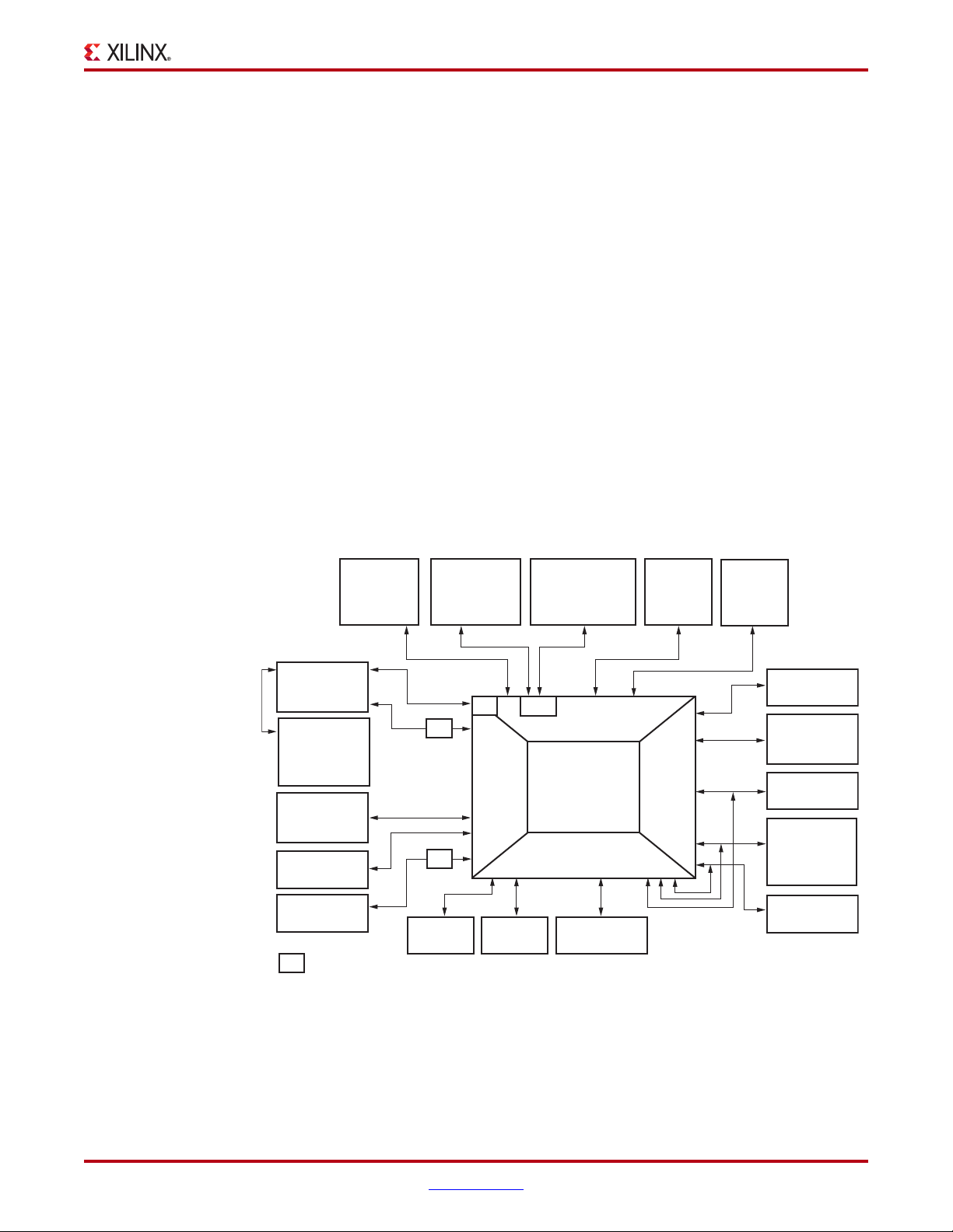
Block Diagram
Overview
Figure 1-1 shows a high-level block diagram of the SP605 and its peripherals.
X-Ref Target - Figure 1-1
Figure 1-1: SP605 Features and Banking
SP605 Hardware User Guide www.xilinx.com 11
UG526 (v1.8) September 24, 2012
Page 12
Chapter 1: SP605 Evaluation Board
15e
13
16b
19
7a
15h
1
2
3
4
8
15g
5
17c
9
3, 14 (on back side)
7b
10
18
6
12
16c
11
17b
15b 15a
17a
19b
15d
UG526_02 _092412
15c
8
7c
16d
17d
16a
15f
Related Xilinx Documents
Prior to using the SP605 Evaluation Board, users should be familiar with Xilinx resources.
See the following locations for additional documentation on Xilinx tools and solutions:
•ISE: www.xilinx.com/ise
• Answer Browser: www.xilinx.com/support
• Intellectual Property: www.xilinx.com/ipcenter
Detailed Description
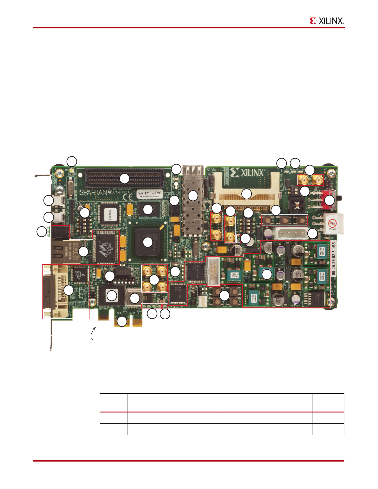
Figure 1-2 shows a board photo with numbered features corresponding to Tab le 1-1 and
the section headings in this document.
X-Ref Target - Figure 1-2
Figure 1-2: SP605 Board
The numbered features in Figure 1-2 correlate to the features and notes listed in Ta bl e 1-1 .
Table 1-1: SP605 Features
Number Feature Notes
12 www.xilinx.com SP605 Hardware User Guide
1 Spartan-6 FPGA XC6SLX45T-3FGG484 FPGA 2–7
2 DDR3 Component Memory Micron MT41J64M16LA-187E 9
Schematic
Page
UG526 (v1.8) September 24, 2012
Page 13
Table 1-1: SP605 Features (Cont’d)
Detailed Description
Number Feature Notes
SPI Header Ext. x4
3
SPI Flash x4 (on backside)
4 Linear BPI Flash x16 Numonyx JS28F256P30T95 19
System ACE CompactFlash
5
Socket
USB UART (USB-to-UART
6
Bridge)
Clock Generation
7
8
9 PCIe 1-lane edge conn.(Gen 1) Card Edge Connector, 1-lane 12
10 SFP Module Cage/Connector AMP 136073-1 12
a. 200 MHz oscillator SiTime 200 MHz 2.5V LVDS 14
b. Oscillator socket, singleended, LVCMOS
c. SMA connectors SMA pair P(J41) / N(J38) 13
GTP port SMA x4 and
MGT Clocking SMA (REFCLK)
Winbond W25Q64VSFIG 18
XCCACE-TQ144I Controller 20
Silicon Labs CP2103GM 32
200 MHz OSC, oscillator socket,
SMA connectors
MMD Components 2.5V 27 MHz 14
MGT RX,TX Pairs x4 SMA MGT
REFCLK x2 SMA
Schematic
Page
13, 14
13
11 Ethernet 10/100/1000 Marvell M88E1111 EPHY 11
12 USB JTAG Conn. (USB Mini-B) USB JTAG Download Circuit 15
13 DVI Codec and Video Connector Chrontel CH7301C-TF 16,17
14 IIC EEPROM (on backside) ST Micro M24C08-WDW6TP 15
10, 11, 14,
15
Status LEDs
a. FMC Power Good 10
b. System ACE CF Status 11
c. FPGA INIT and DONE 14
d. Ethernet PHY Status 18
e. JTAG USB Status 20
f. FPGA Awake 27
g. TI Power Good 31
h. MGT AVCC, DDR3 Term
Pwr Good
18, 20, 25,
27, 31, 33
33
SP605 Hardware User Guide www.xilinx.com 13
UG526 (v1.8) September 24, 2012
Page 14
Chapter 1: SP605 Evaluation Board
Table 1-1: SP605 Features (Cont’d)
Number Feature Notes
a. User LEDs (4) Red LEDs (active-High) 14
16
17
18 FMC LPC Connector Samtec ASP-134603-01 10
19
b. User Pushbuttons (4) Active-High 14
c. User DIP Switch (4-pole) 4-pole (active-High) 14
d. User SMA (2) GPIO x2 SMA 13
Switches
a. SP605 Power On-Off Slide
Switch
b. FPGA Mode DIP Switch 18
c. System ACE CF
Configuration DIP Switch
d . F P GA PR OG , CP U Re se t,
and System ACE CF Reset
Pushbutton Switches
a. Power Management
Controller
b. Mini-Fit Type 6-Pin, ATX
Type 4-pin
Power, Configuration,
Pushbutton Switches
2x TI UCD9240PFC 21, 26
12V input power connectors 25
Schematic
Page
14, 18, 20,
25
25
20
14, 20
1. Spartan-6 XC6SLX45T-3FGG484 FPGA
A Xilinx Spartan-6 XC6SLX45T-3FGG484 FPGA is installed on the SP605 Evaluation Board.
References
See the Spartan-6 FPGA Data Sheet. [Ref 1]
Configuration
The SP605 supports configuration in the following modes:
•JTAG (using the included USB-A to Mini-B cable)
• JTAG (using System ACE CF and CompactFlash card)
•Master SPI x4
• Master SPI x4 with off-board device
• Linear BPI Flash
For details on configuring the FPGA, see Configuration Options.
Mode switch SW1 (see Table 1-32, page 60) is set to 10 = Slave SelectMAP to choose the
System ACE CF default configuration.
14 www.xilinx.com SP605 Hardware User Guide
UG526 (v1.8) September 24, 2012
Page 15

Detailed Description
References
See the Spartan-6 FPGA Configuration User Guide for more information. [Ref 2]
SP605 Hardware User Guide www.xilinx.com 15
UG526 (v1.8) September 24, 2012
Page 16
Chapter 1: SP605 Evaluation Board
I/O Voltage Rails
There are four available banks on the XC6SLX45T-3FGG484 device. Banks 0, 1, and 2 are
connected for 2.5V I/O. Bank 3 is used for the 1.5V DDR3 component memory interface of
Spartan-6 FPGA’s hard memory controller. The voltage applied to the FPGA I/O banks
used by the SP605 board is summarized in Ta bl e 1 -2 .
Table 1-2: I/O Voltage Rail of FPGA Banks
FPGA Bank I/O Voltage Rail
References
See the Xilinx Spartan-6 FPGA documentation for more information at
http://www.xilinx.com/support/documentation/spartan-6.htm
02.5V
12.5V
22.5V
31.5V
.
2. 128 MB DDR3 Component Memory
There are 128 MB of DDR3 memory available on the SP605 board. A 1-Gb Micron
MT41J64M16LA-187E (96-ball) DDR3 memory component is accessible through Bank 3 of
the LX45T device. The Spartan-6 FPGA hard memory controller is used for data transfer
across the DDR3 memory interface’s 16-bit data path using SSTL15 signaling. The SP605
board supports the “standard” VCCINT setting of 1.20V ± 5%. This setting provides
memory controller block (MCB) performance of 667 MT/s for DDR3 memory. Signal
integrity is maintained through DDR3 resistor terminations and memory on-die
terminations (ODT), as shown in Tab le 1 -3 and Ta bl e 1- 4.
Table 1-3: Termination Resistor Requirements
Signal Name Board Termination On-Die Termination
MEM1_A[14:0] 49.9Ω to V
MEM1_BA[2:0] 49.9Ω to V
MEM1_RAS_N 49.9Ω to V
MEM1_CAS_N 49.9Ω to V
MEM1_WE_N 49.9Ω to V
MEM1_CS_N 100Ω to GND –
MEM1_CKE 4.7 KΩ to GND –
MEM1_ODT 4.7 KΩ to GND –
TT
TT
TT
TT
TT
–
–
–
–
–
MEM1_DQ[15:0] – ODT
MEM1_UDQS[P,N], MEM1_LDQS[P,N] – ODT
MEM1_UDM, MEM1_LDM – ODT
16 www.xilinx.com SP605 Hardware User Guide
UG526 (v1.8) September 24, 2012
Page 17
Table 1-3: Termination Resistor Requirements (Cont’d)
Signal Name Board Termination On-Die Termination
Detailed Description
MEM1_CK[P,N]
100Ω differential at memory
component
–
Notes:
1. Nominal value of VTT for DDR3 interface is 0.75V.
Table 1-4: FPGA On-Chip (OCT) Termination External Resistor Requirements
U1 FPGA Pin FPGA Pin Number Board Connection for OCT
ZIO M7 No Connect
RZQ K7 100Ω to GROUND
Tab le 1 -5 shows the connections and pin numbers for the DDR3 Component Memory.
Table 1-5: DDR3 Component Memory Connections
U1 FPGA
Pin
K2 MEM1_A0 N3 A0
K1 MEM1_A1 P7 A1
K5 MEM1_A2 P3 A2
M6 MEM1_A3 N2 A3
Schematic Net Name
Pin Number Pin Name
Memory U42
H3 MEM1_A4 P8 A4
M3 MEM1_A5 P2 A5
L4 MEM1_A6 R8 A6
K6 MEM1_A7 R2 A7
G3 MEM1_A8 T8 A8
G1 MEM1_A9 R3 A9
J4 MEM1_A10 L7 A10/AP
E1 MEM1_A11 R7 A11
F1 MEM1_A12 N7 A12/BCN
J6 MEM1_A13 T3 NC/A13
H5 MEM1_A14 T7 NC/A14
J3 MEM1_BA0 M2 BA0
J1 MEM1_BA1 N8 BA1
H1 MEM1_BA2 M3 BA2
R3 MEM1_DQ0 G2 DQ6
R1 MEM1_DQ1 H3 DQ4
P2 MEM1_DQ2 E3 DQ0
SP605 Hardware User Guide www.xilinx.com 17
UG526 (v1.8) September 24, 2012
Page 18
Chapter 1: SP605 Evaluation Board
Table 1-5: DDR3 Component Memory Connections (Cont’d)
U1 FPGA
Pin
P1 MEM1_DQ3 F2 DQ2
L3 MEM1_DQ4 H7 DQ7
L1 MEM1_DQ5 H8 DQ5
M2 MEM1_DQ6 F7 DQ1
M1 MEM1_DQ7 F8 DQ3
T2 MEM1_DQ8 C2 DQ11
T1 MEM1_DQ9 C3 DQ9
U3 MEM1_DQ10 A2 DQ13
U1 MEM1_DQ11 D7 DQ8
W3 MEM1_DQ12 A3 DQ15
W1 MEM1_DQ13 C8 DQ10
Y2 MEM1_DQ14 B8 DQ14
Y1 MEM1_DQ15 A7 DQ12
H2 MEM1_WE_B L3 WE_B
Schematic Net Name
Pin Number Pin Name
Memory U42
M5 MEM1_RAS_B J3 RAS_B
M4 MEM1_CAS_B K3 CAS_B
L6 MEM1_ODT K1 ODT
K4 MEM1_CLK_P J7 CLK_P
K3 MEM1_CLK_N K7 CLK_N
F2 MEM1_CKE K9 CKE
N3 MEM1_LDQS_P F3 LDQS_P
N1 MEM1_LDQS_N G3 LDQS_N
V2 MEM1_UDQS_P C7 UDQS_P
V1 MEM1_UDQS_N B7 UDQS_N
N4 MEM1_LDM E7 LDM
P3 MEM1_UDM D3 UDM
E3 MEM1_RESET_B T2 RESET_B
References
See the Micron Technology, Inc. DDR3 SDRAM Specification for more information. [Ref 12]
Also, see the Spartan-6 FPGA Memory Controller User Guide. [Ref 3]
18 www.xilinx.com SP605 Hardware User Guide
UG526 (v1.8) September 24, 2012
Page 19
3. SPI x4 Flash
SPI Prog
FPGA_D1_MISO2
J17
1
2
3
4
5
6
7
8
9
FPGA_D2_MISO3
FPGA_PROG_B
FPGA_MOSI_CSI_B_MISO0
SPI_CS_B
FPGA_CCLK
FPGA_D0_DIN_MISO_MISO1
UG526_03_092409
GND
VCC3V3
Silkscreen
TMS
TDI
TDO
TCK
GND
3V3
HDR_1X9
U1
FPGA SPI Interface
U32
J17
SPI x4
Flash
Memory
Winbond
W25Q64VSFIG
SPI Program
Header
SPI Select
Jumper
ON = SPI X4 U32
OFF = SPI EXT. J17
SPIX4_CS_B
DIN, DOUT, CCLK
SPI_CS_B
2
J46
1
UG526_04_092409
The Xilinx Spartan-6 FPGA hosts a SPI interface which is visible to the Xilinx iMPACT
configuration tool. The SPI memory device operates at 3.0V; the Spartan-6 FPGA I/Os are
3.3V tolerant and provide electrically compatible logic levels to directly access the SPI flash
through a 2.5V bank. The XC6SLX45T-3FGG484 is a master device when accessing an
external SPI flash memory device.
The SP605 SPI interface has two parallel connected configuration options (Figure 1-3): an
SPI X4 (Winbond W25Q64VSFIG) 64-Mb flash memory device (U32) and a flash
programming header (J17). J17 supports a user-defined SPI mezzanine board. The SPI
configuration source is selected via SPI select jumper J46. For details on configuring the
FPGA, see Configuration Options.
X-Ref Target - Figure 1-3
Detailed Description
Figure 1-3: J17 SPI Flash Programming Header
X-Ref Target - Figure 1-4
SP605 Hardware User Guide www.xilinx.com 19
UG526 (v1.8) September 24, 2012
Figure 1-4: SPI Flash Interface Topology
Page 20
Chapter 1: SP605 Evaluation Board
Table 1-6: SPI x4 Memory Connections
U1 FPGA
Pin
Schematic Net Name
SPI MEM U32 SPI HDR J17
Pin # Pin Name Pin # Pin Name
AB2 FPGA_PROG_B – – 1 –
T14 FPGA_D2_MISO3 1 IO3_HOLD_B 2 –
R13 FPGA_D1_MISO2_R 9 IO2_WP_B 3 –
AA3 SPI_CS_B – – 4 TMS
AB20 FPGA_MOSI_CSI_B_MISO0 15 DIN 5 TDI
AA20 FPGA_D0_DIN_MISO_MISO1 8 IO1_DOUT 6 TDO
Y20 FPGA_CCLK 16 CLK 7 TCK
– – – –8GND
– – – – 9 VCC3V3
(1)
J46.2
Notes:
1. Not a U1 FPGA pin
SPIX4_CS_B 7 CS_B – –
References
See the Winbond Serial Flash Memory Data Sheet for more information. [Ref 13]
See the XPS Serial Peripheral Interface Data Sheet for more information. [Ref 4]
20 www.xilinx.com SP605 Hardware User Guide
UG526 (v1.8) September 24, 2012
Page 21
4. Linear BPI Flash
U1 U25
FPGA
BPI Flash
Interface
Numonyx Type P30
JS28F256P30
ADDR, DATA, CTRL
UG526_05_092409
A Numonyx JS28F256P30 Linear Flash memory (U25) on the SP605 (Figure 1-5) provides
32 MB of non-volatile storage that can be used for configuration as well as software
storage. The Linear Flash is operated in asynchronous mode.
For details on configuring the FPGA, see Configuration Options.
X-Ref Target - Figure 1-5
Detailed Description
Figure 1-5: Linear BPI Flash Interface
Table 1-7: Linear Flash Connections
U1 FPGA Pin Schematic Net Name
N22 FLASH_A0 29 A1
N20 FLASH_A1 25 A2
M22 FLASH_A2 24 A3
M21 FLASH_A3 23 A4
L19 FLASH_A4 22 A5
K20 FLASH_A5 21 A6
H22 FLASH_A6 20 A7
H21 FLASH_A7 19 A8
L17 FLASH_A8 8 A9
K17 FLASH_A9 7 A10
G22 FLASH_A10 6 A11
U25 BPI FLASH
Pin Number Pin Name
G20 FLASH_A11 5 A12
K18 FLASH_A12 4 A13
K19 FLASH_A13 3 A14
H20 FLASH_A14 2 A15
SP605 Hardware User Guide www.xilinx.com 21
UG526 (v1.8) September 24, 2012
J19 FLASH_A15 1 A16
Page 22
Chapter 1: SP605 Evaluation Board
Table 1-7: Linear Flash Connections (Cont’d)
U1 FPGA Pin Schematic Net Name
E22 FLASH_A16 55 A17
E20 FLASH_A17 18 A18
F22 FLASH_A18 17 A19
F21 FLASH_A19 16 A20
H19 FLASH_A20 11 A21
H18 FLASH_A21 10 A22
F20 FLASH_A22 9 A23
G19 FLASH_A23 26 A24
AA20 FPGA_D0_DIN_MISO_MISO1 34 DQ0
R13 FPGA_D1_MISO2 36 DQ1
T14 FPGA_D2_MISO3 39 DQ2
AA6 FLASH_D3 41 DQ3
AB6 FLASH_D4 47 DQ4
U25 BPI FLASH
Pin Number Pin Name
Y5 FLASH_D5 49 DQ5
AB5 FLASH_D6 51 DQ6
W9 FLASH_D7 53 DQ7
T7 FLASH_D8 35 DQ8
U6 FLASH_D9 37 DQ9
AB19 FLASH_D10 40 DQ10
AA18 FLASH_D11 42 DQ11
AB18 FLASH_D12 48 DQ12
Y13 FLASH_D13 50 DQ13
AA12 FLASH_D14 52 DQ14
AB12 FLASH_D15 54 DQ15
V13 FMC_PWR_GOOD_FLASH_RST_B 44 RST_B
R20 FLASH_WE_B 14 WE_B
P22 FLASH_OE_B 32 OE_B
P21 FLASH_CE_B 30 CE_B
T19 FLASH_ADV_B 46 ADV_B
T18 FLASH_WAIT 56 WAIT
22 www.xilinx.com SP605 Hardware User Guide
UG526 (v1.8) September 24, 2012
Page 23

Detailed Description
FPGA Design Considerations for the Configuration Flash
The SP605 has the P30 BPI flash connected to the FPGA dual use configuration pins and is
not shared. It can be used to configure the FPGA, and then controlled post-configuration
via the FPGA fabric. After FPGA configuration, the FPGA design can disable the
configuration flash or access the configuration flash to read/write code or data.
When the FPGA design does not use the configuration flash, the FPGA design must drive
the FLASH_OE_B pin High in order to disable the configuration flash and put the flash
into a quiescent, low-power state. Otherwise, the flash memory can continue to drive its
array data onto the data bus causing unnecessary switching noise and power
consumption.
For FPGA designs that access the flash for reading/writing stored code or data, connect
the FPGA design or EDK embedded memory controller (EMC) peripheral to the flash
through the pins defined in Figure 1-5, page 17.
References
See the Numonyx StrataFlash Embedded Memory Data Sheet for more information. [Ref 14]
In addition, see the Spartan-6 FPGA Configuration User Guide for more information. [Ref 2]
5. System ACE CF and CompactFlash Connector
The Xilinx System ACE CompactFlash (CF) configuration controller allows a Type I or
Type II CompactFlash card to program the FPGA through the JTAG port. Both hardware
and software data can be downloaded through the JTAG port. The System ACE CF
controller supports up to eight configuration images on a single CompactFlash card. The
configuration address switches allow the user to choose which of the eight configuration
images to use.
The CompactFlash (CF) card shipped with the board is correctly formatted to enable the
System ACE CF controller to access the data stored in the card. The System ACE CF
controller requires a FAT16 file system, with only one reserved sector permitted, and a
sector-per-cluster size of more than one (UnitSize greater than 512). The FAT16 file system
supports partitions of up to 2 GB. If multiple partitions are used, the System ACE CF
directory structure must reside in the first partition on the CompactFlash, with the
xilinx.sys file located in the root directory. The xilinx.sys file is used by the System
ACE CF controller to define the project directory structure, which consists of one main
folder containing eight sub-folders used to store the eight ACE files containing the
configuration images. Only one ACE file should exist within each sub-folder. All folder
names must be compliant to the DOS 8.3 short file name format. This means that the folder
names can be up to eight characters long, and cannot contain the following reserved
characters: < > " / \ |. This DOS 8.3 file name restriction does not apply to the actual ACE
file names.
Other folders and files may also coexist with the System ACE CF project within the FAT16
partition. However, the root directory must not contain more than a total of 16 folder
and/or file entries, including deleted entries. When ejecting or unplugging the
CompactFlash device, it is important to safely stop any read or write access to the
CompactFlash device to avoid data corruption.
SP605 Hardware User Guide www.xilinx.com 23
UG526 (v1.8) September 24, 2012
Page 24

Chapter 1: SP605 Evaluation Board
System ACE CF error and status LEDs indicate the operational state of the System ACE CF
controller:
• A blinking red error LED indicates that no CompactFlash card is present
• A solid red error LED indicates an error condition during configuration
• A blinking green status LED indicates a configuration operation is ongoing
• A solid green status LED indicates a successful download
The mode SW1 setting is important because the System ACE CF can fail to configure the
FPGA when the mode pins are set to the master modes (Table 1-32, page 60). A
configuration failure from the master mode can drive INIT_B low, which blocks the System
ACE CF from downloading a configuration ACE file. The FPGA mode pins must be set as
specified in Tab le 1 -3 2 for the System ACE CF configuration solution.
With the mode switch SW1 set to 10 (Slave SelectMAP, Ta bl e 1- 32 ), if a Compact Flash (CF)
card is installed in the CF socket U37, the System ACE CF will attempt to load a bitstream
from the CF card image address pointed to by the image select switch S1.
Every time a CompactFlash card is inserted into the System ACE CF socket, a
configuration operation is initiated. Pressing the System ACE CF reset button reprograms
the FPGA.
Note:
for more details.
System ACE CF configuration is enabled by way of DIP switch S1. See 17. Switches, page 49
The System ACE CF MPU port (Tabl e 1- 8) is connected to the FPGA. This connection
allows the FPGA to use the System ACE CF controller to reconfigure the system or access
the CompactFlash card as a generic FAT file system.
Table 1-8: System ACE CF Connections
U1 FPGA Pin Schematic Net Name
N6 SYSACE_D0 66 MPD00
N7 SYSACE_D1 65 MPD01
U4 SYSACE_D2 63 MPD02
T4 SYSACE_D3 62 MPD03
P6 SYSACE_D4 61 MPD04
P7 SYSACE_D5 60 MPD05
T3 SYSACE_D6 59 MPD06
R4 SYSACE_D7 58 MPD07
V5 SYSACE_MPA00 70 MPA00
(1)
U17 XCCACETQ144I
Pin Number Pin Name
V3 SYSACE_MPA01 69 MPA01
P5 SYSACE_MPA02 68 MPA02
P4 SYSACE_MPA03 67 MPA03
H4 SYSACE_MPA04 45 MPA04
G4 SYSACE_MPA05 44 MPA05
D2 SYSACE_MPA06 43 MPA06
24 www.xilinx.com SP605 Hardware User Guide
UG526 (v1.8) September 24, 2012
Page 25

Table 1-8: System ACE CF Connections (Cont’d)
FMC LPC
TDO
U1
FPGA
TDITSTTDI CFGTDO
CFGTDI
TSTTDO TDO
System ACE CF
3.3V 2.5V
TDI
Buffer
USB Header
J4
J2
J19
U17
UG526_06_092409
Detailed Description
U1 FPGA Pin Schematic Net Name
(1)
U17 XCCACETQ144I
Pin Number Pin Name
AA1 SYSACE_MPBRDY 39 MPBRDY
W4 SYSACE_MPCE 42 MPCE
AA2 SYSACE_MPIRQ 41 MPIRQ
T6 SYSACE_MPOE 77 MPOE
T5 SYSACE_MPWE 76 MPWE
G17 SYSACE_CFGTDI 81 CFGTDI
A21 FPGA_TCK 80 CFGTCK
E18 FPGA_TDI 82 CFGTDO
D20 FPGA_TMS 85 CFGTMS
N19 CLK_33MHZ_SYSACE(2) 93 CLK
Notes:
1. U17 System ACE CF controller 3.3V signals as named are wired to a set of TXB0108 3.3V-to-1.5V level
shifters. The nets between the 1.5V side of the level shifters and the U1 FPGA have the same names
with _LS appended.
2. The System ACE CF clock is sourced from U29 32.000MHz oscillator.
References
See the System ACE CF product page for more information at
http://www.xilinx.com/support/documentation/system_ace_solutions.htm
In addition, see the System ACE CompactFlash Solution Data Sheet. [Ref 5]
6. USB JTAG
JTAG configuration is provided through onboard USB-to-JTAG configuration logic where
a computer host accesses the SP605 JTAG chain through a Type-A (computer host side) to
Type-Mini-B (SP605 side) USB cable. The JTAG chain of the board is illustrated in
Figure 1-6. JTAG configuration is allowable at any time under any mode pin setting. JTAG
initiated configuration takes priority over the mode pin settings.
X-Ref Target - Figure 1-6
.
SP605 Hardware User Guide www.xilinx.com 25
UG526 (v1.8) September 24, 2012
Figure 1-6: JTAG Chain Diagram
Page 26

Chapter 1: SP605 Evaluation Board
FMC bypass jumper J19 must be connected between pins 1-2 (bypass) to enable JTAG
access to the FPGA on the basic SP605 board (without FMC expansion modules installed),
as shown in Figure 1-7. When the VITA 57.1 FMC LPC expansion connector is populated
with an expansion module that has a JTAG chain, jumper J19 must be set to connect pins
2-3 in order to include the FMC expansion module's JTAG chain in the main SP605 JTAG
chain.
X-Ref Target - Figure 1-7
The JTAG chain can be used to program the FPGA and access the FPGA for hardware and
software debug.
J19
Bypass FMC LPC J2 = Jumper 1-2
Include FMC LPC J2 = Jumper 2-3
1
2
3
H - 1x3
FMC_TDI_BUF
SYSACE_TDI
FMC_TD0
UG526_07_092409
Figure 1-7: VITA 57.1 FMC LPC (J2) JTAG Bypass Jumper J19
The JTAG connector (USB Mini-B J4) allows a host computer to download bitstreams to the
FPGA using the Xilinx iMPACT software tool. In addition, the JTAG connector allows
debug tools such as the ChipScope® Pro Analyzer tool or a software debugger to access the
FPGA. The iMPACT software tool can also program the BPI flash via the USB J4
connection. iMPACT can download a temporary design to the FPGA through the JTAG.
This provides a connection within the FPGA from the FPGAs JTAG port to the FPGAs BPI
interface. Through the connection made by the temporary design in the FPGA, iMPACT
can indirectly program the BPI flash from the JTAG USB J4 connector. For an overview on
configuring the FPGA, see Configuration Options, page 60.
7. Clock Generation
There are three clock sources available on the SP605.
Oscillator (Differential)
The SP605 has one 2.5V LVDS differential 200 MHz oscillator (U6) soldered onto the board
and wired to an FPGA global clock input.
• Crystal oscillator: SiTime SiT9102AI-243N25E200.00000
• Frequency stability: 50 ppm
References
See the SiTime SiT9102 Data Sheet for more information. Search SiT9102 at SiTime.com
[Ref 15].
26 www.xilinx.com SP605 Hardware User Guide
UG526 (v1.8) September 24, 2012
Page 27

Detailed Description
Silkscreened outline
has beveled corner
UG526_08_100509
Socket has notch
in crossbar
Oscillator Socket (Single-Ended, 2.5V or 3.3V)
One populated single-ended clock socket (X2) is provided for user applications. The option
of 2.5V or 3.3V power may be selected via a 0Ω resistor selection. The SP605 board is
shipped with a 27 MHz 2.5V oscillator installed.
Figure 1-8 shows the unpopulated user oscillator socket. This figure indicates the socket
pin 1 location. Figure 1-9 shows the oscillator installed, with its pin 1 location identifiers.
X-Ref Target - Figure 1-8
Figure 1-8: SP605 X2 Oscillator Socket Pin 1 Location Identifiers
X-Ref Target - Figure 1-9
Oscillator top has
corner dot marking
Oscillator body has
one square corner
UG526_09_100509
Figure 1-9: SP605 X2 Oscillator Pin 1 Location Identifiers
SP605 Hardware User Guide www.xilinx.com 27
UG526 (v1.8) September 24, 2012
Page 28

Chapter 1: SP605 Evaluation Board
SMA Connectors (Differential)
A high-precision clock signal can be provided to the FPGA using differential clock signals
through the onboard 50Ω SMA connectors J38 (N) and J41 (P).
Table 1-9: SP605 Clock Source Connections
Source U1 FPGA Pin Schematic Net Name
K22 SYSCLK_N 5 OUT_B
U6 200MHZ OSC
K21 SYSCLK_P 4 OUT
X2 27MHZ OSC AB13 USER_CLOCK 5 OUT
USER_SMA_CLOCK M19 USER_SMA_CLOCK_N J38.1 –
SMA Connectors M20 USER_SMA_CLOCK_P J41.1 –
8. Multi-Gigabit Transceivers (GTP MGTs)
The SP605 provides access to 4 MGTs.
• One (1) MGT is wired to the PCIe x1 Endpoint (P4) edge connector fingers
• One (1) MGT is wired to the FMC LPC connector (J2)
• One (1) MGT is wired to MGT SMA connectors (J36, J37)
• One (1) MGT is wired to the SFP Module connector (P2)
The SP605 includes a set of six SMA connectors for the GTP (MGT) RX/TX Port and GTP
(MGT) Clock as described in Figure 1-10 and Ta bl e 1-1 0.
Pin
Number
Pin Name
28 www.xilinx.com SP605 Hardware User Guide
UG526 (v1.8) September 24, 2012
Page 29

X-Ref Target - Figure 1-10
SMA_RX_N
SMA_RX_P
1
C33
1
C34
2
10V
0.1UF
2
10V
0.1UF
SMA_RX_C_N
X5R
SMA_RX_C_P
X5R
Detailed Description
J35 32K10K-400E3
GND1
GND2
SIG
SIG
GND3
GND4
GND5
GND6
GND7
32K10K-400E3J34
GND1
GND2
GND3
GND4
GND5
GND6
GND7
1
1
2
3
4
5
6
7
8
2
3
4
5
6
7
8
SMA MGT Connectors
SMA_TX_N
SMA_TX_P
MGT REFCLK
SMA_REFCLK_N
SMA_REFCLK_P
1
C35
1
C36
2
10V
0.1UF
2
10V
0.1UF
SMA_REFCLK_C_N
X5R
SMA_REFCLK_C_P
X5R
J33 32K10K-400E3
GND1
GND2
1
1
1
1
GND3
GND4
SIG
GND5
GND6
GND7
32K10K-400E3J32
GND1
GND2
GND3
SIG
GND4
GND5
GND6
GND7
32K10K-400E3J36
GND1
GND2
GND3
GND4
SIG
GND5
GND6
GND7
J37 32K10K-400E3
GND1
GND2
GND3
GND4
SIG
GND5
GND6
GND7
2
3
4
5
6
7
8
2
3
4
5
6
7
8
2
3
4
5
6
7
8
2
3
4
5
6
7
8
UG526_10 _092409
Figure 1-10: GTP SMA Clock
SP605 Hardware User Guide www.xilinx.com 29
UG526 (v1.8) September 24, 2012
Page 30

Chapter 1: SP605 Evaluation Board
Table 1-10: GTP SMA Clock Connections
U1 FPGA Pin Schematic Net Name SMA Pin
C9 SMA_RX_N J35.1
D9 SMA_RX_P J34.1
A8 SMA_TX_N J33.1
B8 SMA_TX_P J32.1
D11 SMA_REFCLK_N J36.1
C11 SMA_REFCLK_P J37.1
30 www.xilinx.com SP605 Hardware User Guide
UG526 (v1.8) September 24, 2012
Page 31

9. PCI Express Endpoint Connectivity
The 1-lane PCIe edge connector performs data transfers at the rate of 2.5 GT/s for a Gen1
application. The Spartan-6 FPGA GTP MGT is used for the multi-gigabit per second serial
interface.
The SP605 board trace impedance on the PCIe lane supports Gen1 applications. The SP605
supports Gen1 x1.
Table 1-11: PCIe Edge Connector Connections
Detailed Description
U1 FPGA Pin Schematic Net Name
P4 PCIe Edge Connector
Pin Number Pin Name
C7 PCIE_RX0_N B15 PETn0
D7 PCIE_RX0_P B14 PETp0
A6 PCIE_TX0_N
B6 PCIE_TX0_P
– PCIE_CLK_QO_N
– PCIE_CLK_QO_P
B10 PCIE_250M_N
A10 PCIE_250M_P
J7 PCIE_PERST_B_LS A11 PERST
(1)
(1)
(3)(6)
(3)(6)
A17 PERn0
A16 PERp0
(2)
(2)
A14 REFCLK-
A13 REFCLK+
(4)
U48.17
(4)
U48.18
NQ
Q
(5)
Notes:
1. Each of the TX0_N/P signals has a 0.1 µF series capacitor.
2. PCIE_CLK_QO_N/P is the PC motherboard 100MHZ REFCLK.
3. Each of the PCIE_250M_N/P signals has a 0.1 µF series capacitor.
4. U48 is an ICS874001 clock multiplier device (U48.17/18 are not P4 pins).
5. The PERST signal from pin P4.A11 is isolated by a series resistor and then level-shifted by U52 before
making the FPGA pin U1.J7 connection.
6. PCIE_250M_N/P signals can be a frequency other than 250 MHz, depending on the settings selected
by resistor population for U48 ICS874001. The default setting is 125 MHz.
The PCIe interface obtains its power from the DC power supply provided with the SP605
or through the 12V ATX power supply connector. The PCIe edge connector is not used for
any power connections.
The board can be powered by one of two 12V sources; J18, a 6-pin (2x3) Mini-Fit-type
connector and J27, a 4-pin (inline) ATX disk drive type connector.
The 6-pin Mini-Fit-type connector provides 60W (12V @ 5A) from the AC power adapter
provided with the board while the 4-pin ATX disk drive type connector is provided for
users who want to power their board while it is installed inside a PC chassis.
For applications requiring additional power, such as the use of expansion cards drawing
significant power, a larger AC adapter might be required. If a different AC adapter is used,
its load regulation should be better than ±10%.
SP605 power slide switch SW2 turns the board on and off by controlling the 12V supply to
the board.
Caution!
and the 4-pin ATX disk drive type connector (J27) at the same time as this will result in damage
to the board. Never connect an auxiliary PCIe 6-pin power connector to J18 6-pin Mini-Fit type
connector on the SP605 board as this could result in damage to the PCIe motherboard and/or
SP605 Hardware User Guide www.xilinx.com 31
UG526 (v1.8) September 24, 2012
Caution! Never apply power to the power brick 6-pin Mini-Fit type connector (J18)
Page 32

Chapter 1: SP605 Evaluation Board
SP605 board. The 6-pin Mini-Fit type connector is marked with a no PCIe power label to warn
users of the potential hazard.
References
See the Spartan-6 FPGA GTP Transceivers User Guide for more information. [Ref 6]
Also, see the following websites for more information about the Spartan-6 FPGA Integrated
Endpoint Block for PCI Express:
• Product information,
http://www.xilinx.com/products/ipcenter/S6_PCI_Express_Block.htm
• IP data sheets, http://www.xilinx.com/support/documentation/ipbusinterfacei-
o_pci-express.htm#131486
In addition, see the PCI Express specifications for more information. [Ref 16]
32 www.xilinx.com SP605 Hardware User Guide
UG526 (v1.8) September 24, 2012
Page 33

10. SFP Module Connector
The board contains a small form-factor pluggable (SFP) connector and cage assembly that
accepts SFP modules. The SFP interface is connected to MGT Bank 123 on the FPGA. The
SFP module serial ID interface is connected to the “SFP” IIC bus (see 14. IIC Bus, page 38
for more information). The control and status signals for the SFP module are connected to
jumpers and test points as described in Tab le 1 -12 . The SFP module connections are shown
in Tab le 1 -1 3.
Table 1-12: SFP Module Control and Status
SFP Control/Status Signal Board Connection
SFP_TX_FAULT
SFP_TX_DISABLE
SFP_MOD_DETECT
Detailed Description
Tes t P o in t J 1 5
High = Fault
Low = Normal Operation
Jumper J44
On = SFP Enabled
Off = SFP Disabled
Tes t P o in t J 1 6
High = Module Not Present
Low = Module Present
Jumper J22
SFP_RT_SEL
Jumper Pins 1-2 = Full Bandwidth
Jumper Pins 2-3 = Reduced Bandwidth
Tes t P o in t J 1 4
SFP_LOS
High = Loss of Receiver Signal
Low = Normal Operation
Table 1-13: SFP Module Connections
U1 FPGA Pin Schematic Net Name
D13 SFP_RX_P 13 RDP
C13 SFP_RX_N 12 RDN
B14 SFP_TX_P 18 TDP
A14 SFP_TX_N 19 TDN
T17 SFP_LOS 8 LOS
Y8 SFP_TX_DISABLE_FPGA 3 TX_DISABLE
A12 SFPCLK_QO_N
B12 SFPCLK_QO_P
(1)
(1)
P2 SFP Module Connector
Pin Number Pin Name
(2)
U47.6
U47.7
(2)
-
-
Notes:
1. The 125MHz SFP clock is sourced by clock driver U47.
2. Not P2 SFP module pins.
SP605 Hardware User Guide www.xilinx.com 33
UG526 (v1.8) September 24, 2012
Page 34

Chapter 1: SP605 Evaluation Board
11. 10/100/1000 Tri-Speed Ethernet PHY
The SP605 uses the onboard Marvell Alaska PHY device (88E1111) for Ethernet
communications at 10, 100, or 1000 Mb/s. The board supports a GMII interface from the
FPGA to the PHY. The PHY connection to a user-provided Ethernet cable is through a Halo
HFJ11-1G01E RJ-45 connector with built-in magnetics.
On power-up, or on reset, the PHY is configured to operate in GMII mode with PHY
address 0b00111 using the settings shown in Ta bl e 1-1 4. These settings can be overwritten
via software commands passed over the MDIO interface.
Table 1-14: PHY Configuration Pins
Connection on
Pin
CFG2 V
CFG3 V
CFG4 V
CFG5 V
CFG6 PHY_LED_RX SEL_BDT = 0 INT_POL = 1 75/50Ω = 0
Board
2.5V ANEG[3] = 1 ANEG[2] = 1 ANEG[1] = 1
CC
2.5V ANEG[0] = 1 ENA_XC = 1 DIS_125 = 1
CC
2.5V HWCFG_MD[2] = 1 HWCFG_MD[1] = 1 HWCFG_MD[0] = 1
CC
2.5V DIS_FC = 1 DIS_SLEEP = 1 HWCFG_MD[3] = 1
CC
Definition and Value
Bit[2]
Bit[1]
Definition and Value
Bit[0]
Definition and Value
Tab le 1 -1 5 shows the connections and pin numbers for the PHY.
Table 1-15: Ethernet PHY Connections
U1 FPGA Pin Schematic Net Name
Pin Number Pin Name
V20 PHY_MDIO 33 MDIO
R19 PHY_MDC 35 MDC
J20 PHY_INT 32 INT_B
J22 PHY_RESET 36 RESET_B
N15 PHY_CRS 115 CRS
U46 M88E111
M16 PHY_COL 114 COL
P20 PHY_RXCLK 7 RXCLK
U20 PHY_RXER 8 RXER
T22 PHY_RXCTL_RXDV 4 RXDV
P19 PHY_RXD0 3 RXD0
Y22 PHY_RXD1 128 RXD1
Y21 PHY_RXD2 126 RXD2
W22 PHY_RXD3 125 RXD3
W20 PHY_RXD4 124 RXD4
V22 PHY_RXD5 123 RXD5
V21 PHY_RXD6 121 RXD6
34 www.xilinx.com SP605 Hardware User Guide
UG526 (v1.8) September 24, 2012
Page 35

Table 1-15: Ethernet PHY Connections (Cont’d)
Detailed Description
U1 FPGA Pin Schematic Net Name
Pin Number Pin Name
U22 PHY_RXD7 120 RXD7
AB7 PHY_TXC_GTPCLK 14 GTXCLK
L20 PHY_TXCLK 10 TXCLK
U8 PHY_TXER 13 TXER
T8 PHY_TXCTL_TXEN 16 TXEN
U10 PHY_TXD0 18 TXD0
T10 PHY_TXD1 19 TXD1
AB8 PHY_TXD2 20 TXD2
AA8 PHY_TXD3 24 TXD3
AB9 PHY_TXD4 25 TXD4
Y9 PHY_TXD5 26 TXD5
Y12 PHY_TXD6 28 TXD6
W12 PHY_TXD7 29 TXD7
U46 M88E111
References
See the Marvell Alaska Gigabit Ethernet Transceivers product page for more information.
[Ref 17]
Also, see the LogiCORE™ IP Tri-Mode Ethernet MAC User Guide. [Ref 7]
SP605 Hardware User Guide www.xilinx.com 35
UG526 (v1.8) September 24, 2012
Page 36

Chapter 1: SP605 Evaluation Board
12. USB-to-UART Bridge
The SP605 contains a Silicon Labs CP2103GM USB-to-UART bridge device (U4) which
allows connection to a host computer with a USB cable. The USB cable is supplied in this
evaluation kit (Type A end to host computer, Type Mini-B end to SP605 connector J23).
Tab le 1 -1 6 details the SP605 J23 pinout.
Xilinx UART IP is expected to be implemented in the FPGA fabric (for instance, Xilinx XPS
UART Lite). The FPGA supports the USB-to-UART bridge using four signal pins: Transmit
(TX), Receive (RX), Request to Send (RTS), and Clear to Send (CTS).
Silicon Labs provides royalty-free Virtual COM Port (VCP) drivers which permit the
CP2103GM USB-to-UART bridge to appear as a COM port to host computer
communications application software (for example, HyperTerm or TeraTerm). The VCP
device driver must be installed on the host PC prior to establishing communications with
the SP605. Refer to the evaluation kit Getting Started Guide for driver installation
instructions.
Table 1-16: USB Type B Pin Assignments and Signal Definitions
USB Connector
Pin
1 VBUS +5V from host system (not used)
2 USB_DATA_N Bidirectional differential serial data (N-side)
3 USB_DATA_P Bidirectional differential serial data (P-side)
4 GROUND Signal ground
Signal Name Description
Table 1-17: USB-to-UART Connections
U1 FPGA Pin
F18 RTS, output USB_1_CTS 22 CTS, input
F19 CTS, input USB_1_RTS 23 RTS, output
B21 TX, data out USB_1_RX 24 RXD, data in
H17 RX, data in USB_1_TX 25 TXD, data out
Notes:
1. The schematic net names correspond with the CP2103GM pin names and functions, and the UART IP
in the FPGA must be connected accordingly.
UART Function
in FPGA
Schematic Net
Name
U30 CP2103GM
Pin
UART Function
in CP2103GM
References
Refer to the Silicon Labs website for technical information on the CP2103GM and the VCP
drivers.
In addition, see some of the Xilinx UART IP specifications at:
• http://www.xilinx.com/support/documentation/ip_documentation/xps_uartlite.pdf
//
• http:
36 www.xilinx.com SP605 Hardware User Guide
www.xilinx.com/support/documentation/ip_documentation/xps_uart16550.pdf
UG526 (v1.8) September 24, 2012
Page 37

13. DVI CODEC
A DVI connector (P3) is present on the board to support an external video monitor. The
DVI circuitry utilizes a Chrontel CH7301C (U31) capable of 1600 X 1200 resolution with 24bit color. The video interface chip drives both the digital and analog signals to the DVI
connector. A DVI monitor can be connected to the board directly. A VGA monitor can also
be connected to the board using the supplied DVI-to-VGA adaptor. The Chrontel CH7301C
is controlled by way of the video IIC bus.
The DVI connector (Ta bl e 1- 18 ) supports the IIC protocol to allow the board to read the
monitor's configuration parameters. These parameters can be read by the FPGA using the
DVI IIC bus (see 14. IIC Bus, page 38).
Table 1-18: DVI Controller Connections
Detailed Description
U1 FPGA Pin
K16 DVI_D0 63 D0
U19 DVI_D1 62 D1
T20 DVI_D2 61 D2
N16 DVI_D3 60 D3
P16 DVI_D4 59 D4
M17 DVI_D5 58 D5
M18 DVI_D6 55 D6
R15 DVI_D7 54 D7
R16 DVI_D8 53 D8
P17 DVI_D9 52 D9
P18 DVI_D10 51 D10
R17 DVI_D11 50 D11
J17 DVI_DE 2 DE
J16 DVI_H 4 H
Schematic Net
Name
U31 Chrontel CH7301C
Pin Number Pin Name
L15 DVI_RESET_B 13 RESET_B
B22 DVI_V 5 V
C22 DVI_XCLK_N 56 XCLK_N
C20 DVI_XCLK_P 57 XCLK_P
No Connect DVI_GPIO0 8 GPIO0
D22 DVI_GPIO1 7 GPIO1
SP605 Hardware User Guide www.xilinx.com 37
UG526 (v1.8) September 24, 2012
Page 38

Chapter 1: SP605 Evaluation Board
14. IIC Bus
The SP605 implements three IIC bus interfaces at the FPGA.
The MAIN IIC bus hosts four items:
• FPGA U1 Bank 1 “MAIN” IIC interface
•8-Kb NV Memory U4
• FMC LPC connector J2
• 2-Pin External Access Header J45
The DVI IIC bus hosts two items:
• FPGA U1 Bank 2 DVI IIC interface
• DVI Codec U31 and DVI connector P3
The SFP IIC bus hosts two items:
• FPGA U1 Bank 0 SFP IIC interface
• SFP module connector P2
The SP605 IIC bus topology is shown in Figure 1-11.
X-Ref Target - Figure 1-11
U1
IIC_SDA_MAIN
BANK 1
BANK 0
FPGA IIC
INTERFACE
BANK 2
P3
DVI Connector
Addr: 0b1010000
IIC_SCL_MAIN
IIC_SDA_SFP
IIC_SCL_SFP
IIC_SDA_DVI
IIC_SCL_DVI
IIC_CLK_DVI_F
IIC_SDA_DVI_F
LEVEL
SHIFTER
U4
ST MICRO
M24C08-WDW6TP
Addr: 0b1010100
through
0b1010111
J2
FMC LPC
Column C
2 Kb EEPROM on
any FMC LPC
Mezzanine Card
Addr: 0b1010010
J45
2-Pin External
Access Header
U31
DVI CODEC
CHRONTEL
CH730C-TF
Addr: 0b1110110
Addr: 0b1010000
P2
SFP Module
Connector
UG526_11_092609
Figure 1-11: IIC Bus Topology
38 www.xilinx.com SP605 Hardware User Guide
UG526 (v1.8) September 24, 2012
Page 39

Table 1-19: IIC Bus Connections
VCC3V3
VCC3V3
SCL
SDA
A0
A1
A2
WP
VCC
GND
IIC Address 0b1010100
External Access
Header
1
2
R292
0
1/16W
5%
2
1
5%
1/16W
0
R291
2
1
5%
1/10W
1.0K
R6
IIC_SDA_MAIN
IIC_SCL_MAIN
12
H-1X2
J45
6
5
1
2
3
7
8
4
U4
M24C08-WDW6TP
2
1
C40
0.1UF
10V
X5R
1
2
R5
1.0K
1/10W
5%
1
2
R216
1
2
1%
1/16W
50
R50
UG526_12 _012611
DNP
Detailed Description
U1 FPGA Pin
Schematic
Netname
Connected To
R22 IIC_SDA_MAIN J2.C31, U4.5
T21 IIC_SCL_MAIN J2.C30, U4.6
(1)
(1)
Level-Shifted
Connection
Level-Shifted
Net Name
– –
– –
AA4 IIC_SDA_DVI Q8.2, U31.14 Q8.3, P3.7 IIC_SDA_DVI_F
W13 IIC_SCL_DVI Q7.2, U31.15 Q7.3, P3.6 IIC_CLK_DVI_F
E6 IIC_SDA_SFP P2.4 – –
E5 IIC_SCL_SFP P2.5 – –
Notes:
1. U4 IIC bus signals are resistively coupled with 0Ω resistors
2. Legend
J2, FMC LPC Connector
P2, SFP Module Connector
P3, DVI Connector
Qn.n, Level-Shifting Transistor
U31, Chrontel CH7301C
IIC External Access Header
J45 (see Figure 1-12) is a two-pin header that allows external IIC devices to be connected to
the SP605 IIC bus. When connected, the external device can be accessed via IIC commands
using IIC_SDA_MAIN and IIC_SCL_MAIN.
8-Kb NV Memory
The SP605 hosts a 8-Kb ST Microelectronics M24C08-WDW6TP IIC parameter storage
memory device (U4). The IIC address of U4 is 0b1010100, and U4 is not write protected
(WP pin 7 is tied to GND).
The IIC memory is shown in Figure 1-12.
X-Ref Target - Figure 1-12
SP605 Hardware User Guide www.xilinx.com 39
UG526 (v1.8) September 24, 2012
Figure 1-12: IIC Memory U4
Page 40

Chapter 1: SP605 Evaluation Board
Table 1-20: IIC Memory Connections
U1 FPGA Pin Schematic Netname
Not Applicable Tied to GND 1 A0
Not Applicable Tied to GND 2 A1
Not Applicable Pulled up (0Ω) to VCC3V3 3 A2
R22 IIC_SDA_MAIN 5 SDA
T21 IIC_SCL_MAIN 6 SCL
Not Applicable Tied to GND 7 WP
IIC Memory U4
Pin Number Pin Name
References
See the ST Micro M24C08 Data Sheet for more information. [Ref 18]
In addition, see the Xilinx XPS IIC Bus Interface Data Sheet. [Ref 8]
40 www.xilinx.com SP605 Hardware User Guide
UG526 (v1.8) September 24, 2012
Page 41

Detailed Description
15. Status LEDs
Tab le 1 -2 1 defines the status LEDs.
Table 1-21: Status LEDs
Reference
Designator
DS1 FMC_PWR_GOOD_FLASH_RST_B Green FMC PWR GD FMC Power Good
DS2 FPGA_DONE Green DONE FPGA DONE
DS3 GPIO_LED_0 Green GPIO_LED_0
DS4 GPIO_LED_1 Green GPIO_LED_1
DS5 GPIO_LED_2 Green GPIO_LED_2
DS6 GPIO_LED_3 Green GPIO_LED_3
DS7 FPGA_AWAKE Green FPGA AWAKE
Signal Name Color Label Description
DS8 SYSACE_STAT_LED Green
DS9
DS10 LED_RED / LED_GRN Red/Green STATUS USB JTAG Controller Status
DS14 VCC12_P Green 12V 12V Power On
DS15 (U11.9 PGOOD PIN) Green DDR3 PWR GD DDR3 1.5V Power On
DS17 FPGA_INIT_B Red INIT FPGA INIT
DS18 SYSACE_ERR_LED Red
DS19 MGT_POWERGOOD Green MGT_AVCC GD MGT_AVCC Power On
TI_PWRGOOD (AND)
MGT_TI_PWRGOOD
Green POWER GOOD
System ACE CF
Status LED
System ACE CF
Error LED
System ACE CF Status
TI_CORE_PWR+TI_MGT_PWR
GOOD
System ACE CF Error
SP605 Hardware User Guide www.xilinx.com 41
UG526 (v1.8) September 24, 2012
Page 42

Chapter 1: SP605 Evaluation Board
Ethernet PHY Status LEDs
The Ethernet PHY status LEDs (DS11-DS13) are mounted in right-angle plastic housings to
make them visible on the connector end of the board when the SP605 board is installed into
a PC motherboard. This cluster of six LEDs is installed adjacent to the RJ45 Ethernet jack
P1.
X-Ref Target - Figure 1-13
Direction
Indicator
Link Rate
(Mbps)
DUP
TX
RX
10
100
1000
P1
End view of SP605 Ethernet jack and
status LEDs when installed vertically
in a PC chassis
UG526_13 _092409
Figure 1-13: Ethernet PHY Status LEDs
42 www.xilinx.com SP605 Hardware User Guide
UG526 (v1.8) September 24, 2012
Page 43

Detailed Description
FPGA INIT and DONE LEDs
The typical Xilinx FPGA power up and configuration status LEDs are present on the SP605.
The red INIT LED DS17 comes on momentarily after the FPGA powers up and during its
internal power-on process. The DONE LED DS2 comes on after the FPGA programming
bitstream has been downloaded and the FPGA successfully configured.
X-Ref Target - Figure 1-14
VCC2V5
VCC2V5
1
2
R169
332
1%
1/16W
FPGA_DONE
LED-RED-SMT
2
DS17
VCC2V5
1
1
2
R19
4.7K
5%
1/16W
R69
2
1%
75.0
1
FPGA_INIT_B
INIT_B = 0, LED: ON
INIT_B = 1, LED: OFF
Figure 1-14: FPGA INIT and DONE LEDs
Table 1-22: FPGA INIT and DONE LED Connections
U1 FPGA Pin
Schematic Net
Name
Controlled LED
Y4 FPGA_INIT_B DS17 INIT, Red
2
LED-GRN-SMT
1
1
2
UG526_14 _092409
DS2
R70
27.4
1%
1/16W
AB21 FPGA_DONE DS2 DONE, Green
SP605 Hardware User Guide www.xilinx.com 43
UG526 (v1.8) September 24, 2012
Page 44

Chapter 1: SP605 Evaluation Board
R71
27.4
1%
1/16W
1
2
LED-GRN-SMT
2
DS6
1
UG526_15_092409
R72
27.4
1%
1/16W
1
2
LED-GRN-SMT
2
DS5
1
R73
27.4
1%
1/16W
1
2
LED-GRN-SMT
2
DS4
1
R74
27.4
1%
1/16W
1
2
LED-GRN-SMT
2
DS3
1
GPIO LED 3
GPIO LED 2
GPIO LED 1
GPIO LED 0
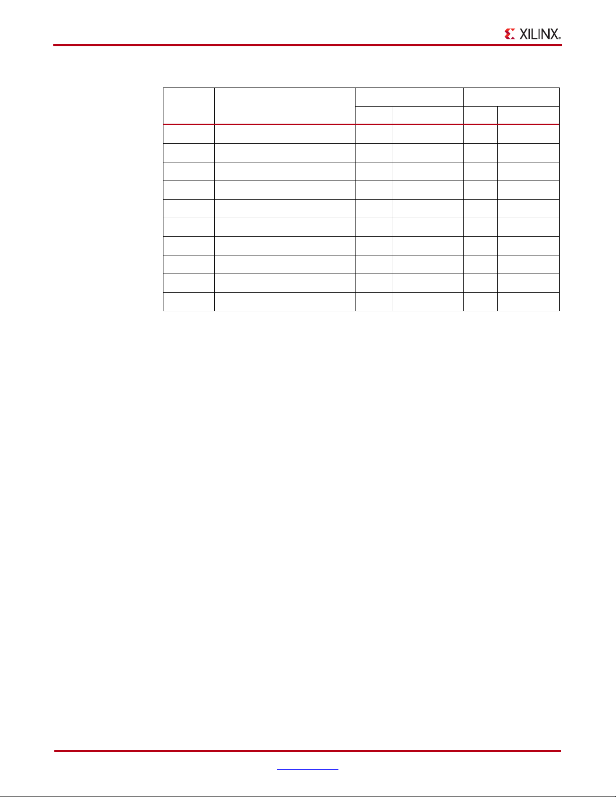
16. User I/O
The SP605 provides the following user and general purpose I/O capabilities:
• User LEDs
• User Pushbutton Switches
• User DIP Switch
• User SIP Header
• User SMA GPIO
User LEDs
The SP605 provides four active-High green LEDs as described in Figure 1-15 and
Tab le 1 -2 3.
X-Ref Target - Figure 1-15
44 www.xilinx.com SP605 Hardware User Guide
Figure 1-15: User LEDs
Table 1-23: User LED Connections
U1 FPGA Pin Schematic Net Name Controlled LED
D17 GPIO_LED_0 DS3
AB4 GPIO_LED_1 DS4
D21 GPIO_LED_2 DS5
W15 GPIO_LED_3 DS6
UG526 (v1.8) September 24, 2012
Page 45

Detailed Description
VCC1V5
CPU_RESET
Pushbutton
1
1
2
4
2
SW6
R230
1.00K
1%
1/16W
3
P1
P2 P3
P4
UG526_16_092409
User Pushbutton Switches
The SP605 provides five active-High pushbutton switches: SW4, SW5, SW6, SW7 and SW8.
The five pushbuttons all have the same topology as the sample shown in Figure 1-16. Four
pushbuttons are assigned as GPIO, and the fifth is assigned as a CPU_RESET. Figure 1-16
and Ta bl e 1 -2 4 describe the pushbutton switches.
X-Ref Target - Figure 1-16
Figure 1-16: User Pushbutton Switch (Typical)
Table 1-24: Pushbutton Switch Connections
U1 FPGA Pin Schematic Netname Switch Pin
F3 GPIO_BUTTON_0 SW4.2
G6 GPIO_BUTTON_1 SW7.2
F5 GPIO_BUTTON_2 SW5.2
C1 GPIO_BUTTON_3 SW8.2
H8 CPU_RESET SW6.2
SP605 Hardware User Guide www.xilinx.com 45
UG526 (v1.8) September 24, 2012
Page 46

Chapter 1: SP605 Evaluation Board
VCC2V5
VCC1V5_FPGA
1
2
3
4
1234
8
7
6
5
S2
ON
SDMX-4-X
GPIO_SWITCH_3
GPIO_SWITCH_2
GPIO_SWITCH_1
GPIO_SWITCH_0
1
2
R225
1.00K
1/16W
1%
2
1
1%
1/16W
1.00K
R224
1
2
R223
1.00K
1/16W
1%
2
1
1%
1/16W
1.00K
R222
UG526_17 _102609
User DIP Switch
The SP605 includes an active-High four-pole DIP switch, as described in Figure 1-17 and
Tab le 1 -2 5. Three poles (switches 1-3) are pulled up to 2.5V, and one pole (switch 4) is
pulled up to 1.5V, when closed.
X-Ref Target - Figure 1-17
Figure 1-17: User DIP Switch S2
Table 1-25: User DIP Switch Connections
U1 FPGA Pin Schematic Net Name DIP Switch Pin
C18 GPIO_SWITCH_0 S2.1
Y6 GPIO_SWITCH_1 S2.2
W6 GPIO_SWITCH_2 S2.3
E4 GPIO_SWITCH_3 S2.4
46 www.xilinx.com SP605 Hardware User Guide
UG526 (v1.8) September 24, 2012
Page 47

X-Ref Target - Figure 1-18
VCC3V3
HDR_1x6
GPIO_HEADER_3
GPIO_HEADER_2
GPIO_HEADER_1
GPIO_HEADER_0
2
1
5%
1/16W
200
R281
1
2
R280
200
1/16W
5%
1
2
3
4
5
6
J55
DNP
1
2
R282
200
1/16W
5%
2
1
5%
1/16W
200
R283
TXB0108
VCCB
B1
B2
B3
B4
B6
B7
GND
A3
A8
OE
A4
A5
A7
A6
B5
A1
A2
B8
VCCA
VCC1V5_FPGA VCC3V3
GPIO_HEADER_0
GPIO_HEADER_1
GPIO_HEADER_2
GPIO_HEADER_3
GPIO_HEADER_0_LS
GPIO_HEADER_1_LS
NC
NC
NC
NC
2
12
3
1
15
7
8
6
5
10
9
4
11
13
14
16
17
18
20
19
U52
1
2
X5R
10V
0.1UF
C385
2
1
C384
0.1UF
10V
X5R
NC
NC
NC
NC
GPIO_HEADER_2_LS
GPIO_HEADER_3_LS
U1 FPGA Pin
G7
H6
D1
R7
UG526_18 _092409
Detailed Description
User SIP Header
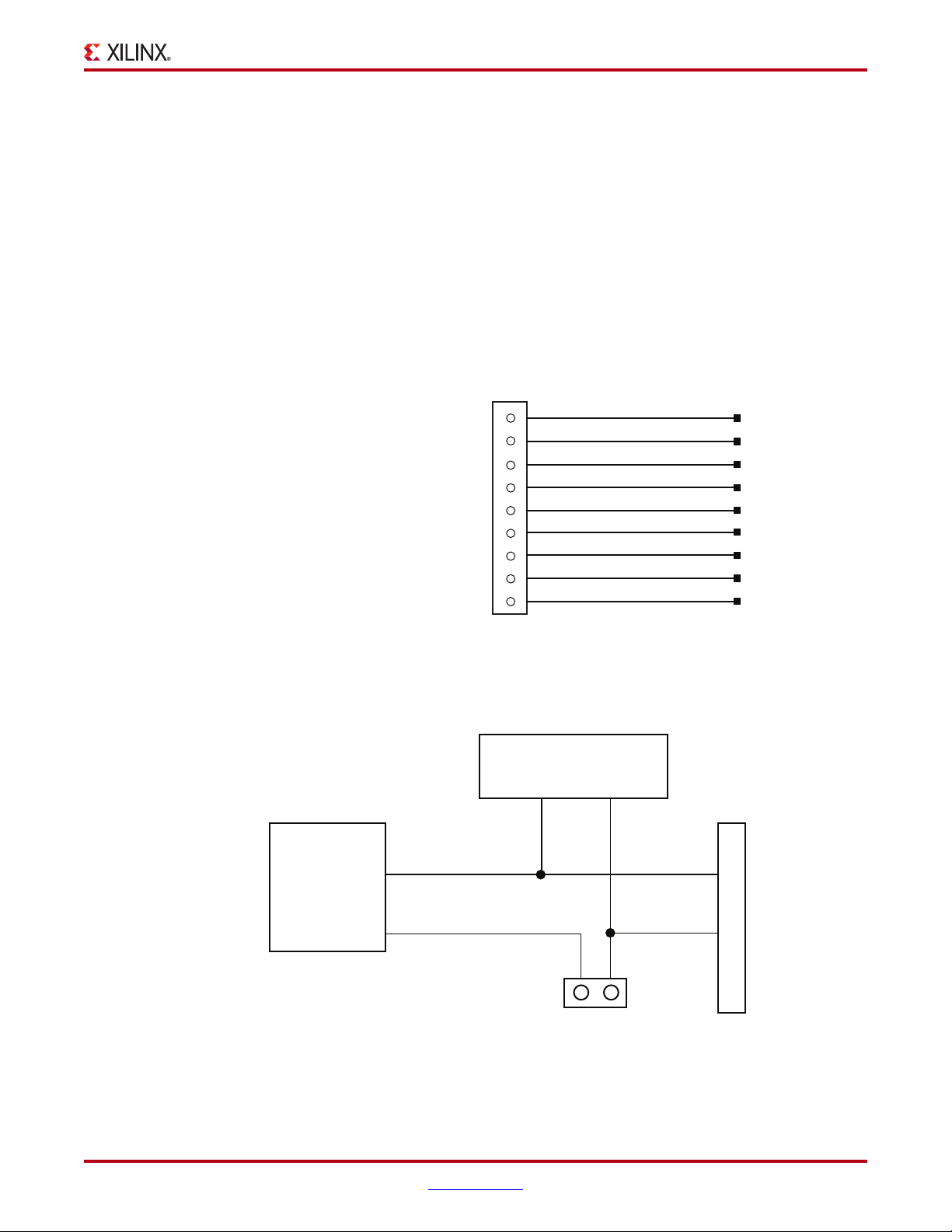
The SP605 includes a 6-pin single-inline (SIP) male pin header (J55) for FPGA GPIO access.
Four pins of J55 are wired to the FPGA through 200Ω series resistors and a level shifter, and
the remaining two J55 pins are wired to 3.3V and GND. The J55 header is described in
Figure 1-18 and Ta bl e 1- 26 .
Figure 1-18: User SIP Header J55
Table 1-26: User SIP Header Connections
U1 FPGA Pin Schematic Net Name GPIO Header Pin
G7 GPIO_HEADER_0 J55.1
H6 GPIO_HEADER_1 J55.2
D1 GPIO_HEADER_2 J55.3
R7 GPIO_HEADER_3 J55.4
–GNDJ55.5
– VCC3V3 J55.6
Notes:
1. Each GPIO_HEADER_n signal is sourced from the FPGA as
<netname>_LS to a level shifter, then to the J55 header.
2. Each GPIO_HEADER_n net has a 200Ω series resistor between the
level shifter and its respective header pin.
SP605 Hardware User Guide www.xilinx.com 47
UG526 (v1.8) September 24, 2012
Page 48

Chapter 1: SP605 Evaluation Board
GND1
GND2
GND3
GND4
GND5
GND6
GND7
SIG
GND1
GND2
GND3
GND4
GND5
GND6
GND7
SIG
USER_SMA_GPIO_P
USER_SMA_GPIO_N
1
8
7
6
5
4
3
2
J40
32K10K-400E3
1
8
7
6
5
4
3
2
32K10K-400E3
J39
UG526_19 _092409
User SMA GPIO
The SP605 includes an pair of SMA connectors for GPIO as described in Figure 1-19 and
Tab le 1 -2 7.
X-Ref Target - Figure 1-19
Figure 1-19: User SMA GPIO
48 www.xilinx.com SP605 Hardware User Guide
Table 1-27: User SMA Connections
U1 FPGA Pin Schematic Net Name GPIO SMA Pin
A3 USER_SMA_GPIO_N J39.1
B3 USER_SMA_GPIO_P J40.1
UG526 (v1.8) September 24, 2012
Page 49

X-Ref Target - Figure 1-20
UG526_20 _100609
N/C
12v
12v
N/C
COM
COM
1
4
2
3
6
1
2
3
4
5
NC
NC
39-30-1060
ATX Peripheral Cable Connector
can plug into J27 when SP605 is
in PC and the desk top AC adapter
(brick) is not used.
J27
J18
12V
COM
COM
5V
NC
350211-1
VCC12_P_IN
1
2
NC
NC
DPDT
VCC12_P
5
2
+
C280
330UF
16V
ELEC
1
3
4
6
SW2
1201M2S3ABE2
12
2
1
R322
1.00K
1%
1/16W
DS25
LED-GRN-SMT
CAUTION!
DO NOT plug a PC ATX power supply 6-pin connector into
the J18 connector on the SP605 board. The ATX 6-pin
connector has a different pinout than J18 and will damage
the SP605 board and void the board warranty.
DO NOT plug an auxilliary PCIe 6-pin molex power
connector into the J18 connector as this could damage the
PCIe motherboard and/or the SP605 board. J18 is marked
with a NO PCIE POWER label to warn users of the poten-
tial hazard.
DO NOT apply power to J18
and the 4-pin ATX disk drive
connector J27 at the same time as this will damage the
SP605 board.
PCIe
Power
Detailed Description
17. Switches
The SP605 Evaluation board includes the following switches:
• Power On/Off Slide Switch SW2
• FPGA_PROG_B Pushbutton SW3 (Active-Low)
• SYSACE_RESET_B Pushbutton SW9 (Active-Low)
• System ACE CF CompactFlash Image Select DIP Switch S1 (Active-High)
• Mode DIP Switch SW1 (Active-High)
Power On/Off Slide Switch SW2
SW2 is the SP605 board main power on/off switch. Sliding the switch actuator from the off
to on position applies 12V power from either J18 (6-pin Mini-Fit) or J27 (4-pin ATX) power
connector to the VCC12_P power plane. Green LED DS14 will illuminate when the SPL605
board power is on. See 19. Power Management, page 55 for details on the on-board power
system.
SP605 Hardware User Guide www.xilinx.com 49
UG526 (v1.8) September 24, 2012
Figure 1-20: Power On/Off Slide Switch SW2
Page 50

Chapter 1: SP605 Evaluation Board
VCC2V5
P2
P1
P3
P4
Pushbutton
1
2
R17
4.7K
1/16W
5%
2
1
3
4
SW3
FPGA_PROG_B
UG526_21 _092409
P2
P1
P3
P4
Pushbutton
Silkscreen:
"SYSACE RESET"
2
1
3
4
SW9
SYSACE_RESET_B
20
UG526_22 _092409
FPGA_PROG_B Pushbutton SW3 (Active-Low)
The SW3 switch (Figure 1-21) grounds the FPGA PROG_B pin when pressed. This action
clears the FPGA. See the Spartan-6 FPGA data sheet for more information on clearing the
contents of the FPGA.
X-Ref Target - Figure 1-21
SYSACE_RESET_B Pushbutton SW9 (Active-Low)
Figure 1-21: FPGA PROG_B Pushbutton SW3
When the System ACE CF configuration mode pin is high (enabled by closing DIP switch
S1 switch 4), the System ACE CF controller configures the FPGA from the CompactFlash
card when a card is inserted or the SYSACE RESET button is pressed. See 5. System ACE
CF and CompactFlash Connector, page 23 for more details.
X-Ref Target - Figure 1-22
Figure 1-22: System ACE CF RESET_B Pushbutton SW9
50 www.xilinx.com SP605 Hardware User Guide
UG526 (v1.8) September 24, 2012
Page 51

Detailed Description
System ACE CF CompactFlash Image Select DIP Switch S1 (Active-High)
System ACE CF CompactFlash (CF) image select DIP switch S1, switches 1–3 (Figure 1-23)
select which CF resident bitstream image is downloaded to the FPGA. S1 switches 1–3 offer
eight binary addresses. When ON (high), the S1 switch 4 enables the System ACE CF
controller to configure the FPGA from the CompactFlash card when a card is inserted or
the SYSACE RESET button is pressed. See 5. System ACE CF and CompactFlash
Connector, page 23 for more details.
X-Ref Target - Figure 1-23
VCC2V5
5%
1
200
2
R134
5%
1
200
2
1/16W
R135
5%
1
200
2
1/16W
R136
1/16W
5
6
7
8
S1
ON
SDMX-4-X
4
3
2
1
1234
1% 1/16W
2
1
R221
1.00K
1
1/16W1%
R220
1% 1/16W
2
1.00K
2
1.00K
1
R219
1/16W1%
SYSACE_CFGMODEPIN
SYSACE_CFGADDR2
SYSACE_CFGADDR1
SYSACE_CFGADDR0
2
1.00K
1
R218
UG526_23 _102709
5%
1
200
2
R133
1/16W
Figure 1-23: System ACE CF CompactFlash Image Select DIP Switch S1
SP605 Hardware User Guide www.xilinx.com 51
UG526 (v1.8) September 24, 2012
Page 52

Chapter 1: SP605 Evaluation Board
Mode DIP Switch SW1 (Active-High)
DIP switch SW1 sets the FPGA mode as shown in Figure 1-24 and Table 1-32, page 60.
X-Ref Target - Figure 1-24
VCC2V5
FPGA_M0_CMP_MISO
FPGA_M1
1/16W
2
1/16W
5%
200
R138
1
2
4
3
200
R139
1
2
5%
1
SW1
1
2
R8
1.0K
5%
1/10W
1
2
R9
1.0K
5%
1/10W
SDMX-2-X
UG526_24 _092409
Figure 1-24: FPGA Mode DIP Switch SW1
References
For more information, refer to the Spartan-6 FPGA Configuration User Guide [Ref 2]. See
Table 1-32, page 60 for the configuration modes.
52 www.xilinx.com SP605 Hardware User Guide
UG526 (v1.8) September 24, 2012
Page 53

18. VITA 57.1 FMC LPC Connector
The SP605 implements the Low Pin Count (LPC, J2) connector option of the VITA 57.1.1
FMC specification.
Detailed Description
Note:
from the SP605 board.
The FMC LPC J2 connector is a keyed connector oriented so that a plug-on card faces away
The FMC standard calls for two connector densities: a High Pin Count (HPC) and a Low
Pin Count (LPC) implementation. A common 10 x 40 position (400 pin locations) connector
form factor is used for both versions. The HPC version is fully populated with 400 pins
present, and the LPC version is partially populated with 160 pins.
The 10 x 40 rows of a FMC LPC connector provides connectivity for:
• 68 single-ended or 34 differential user defined signals
•1 MGT
•1 MGT clock
•2 differential clocks
• 61 ground, 10 power connections
Of the above signal and clock connectivity capability, the SP605 implements the full set:
• 34 differential user-defined pairs
• 34 LA pairs
•1 MGT
•1 MGT clock
•2 differential clocks
Note:
adjustable). The 2.5V rail cannot be turned off. The SP605 VITA 57.1 FMC interfaces are compatible
with 2.5V mezzanine cards capable of supporting 2.5V VADJ.
The SP605 board VADJ voltage for the FMC LPC connector J2 is fixed at 2.5V (non-
SP605 Hardware User Guide www.xilinx.com 53
UG526 (v1.8) September 24, 2012
Page 54

Chapter 1: SP605 Evaluation Board
Tab le 1 -2 8 shows the VITA 57.1 FMC LPC connections. The connector pinout is in
Appendix C, VITA 57.1 FMC LPC Connector Pinout.
Table 1-28: VITA 57.1 FMC LPC Connections
J63 FMC
LPC Pin
D1 FMC_PWR_GOOD_FLASH_RST_B V13
C2 FMC_DP0_C2M_P B16 D4 FMC_GBTCLK0_M2C_P E12
C3 FMC_DP0_C2M_N A16 D5 FMC_GBTCLK0_M2C_N F12
C6 FMC_DP0_M2C_P D15 D8 FMC_LA01_CC_P F14
C7 FMC_DP0_M2C_N C15 D9 FMC_LA01_CC_N F15
C10 FMC_LA06_P D4 D11 FMC_LA05_P C4
C11 FMC_LA06_N D5 D12 FMC_LA05_N A4
C14 FMC_LA10_P H10 D14 FMC_LA09_P F7
C15 FMC_LA10_N H11 D15 FMC_LA09_N F8
C18 FMC_LA14_P C17 D17 FMC_LA13_P G16
C19 FMC_LA14_N A17 D18 FMC_LA13_N F17
C22 FMC_LA18_CC_P T12 D20 FMC_LA17_CC_P Y11
C23 FMC_LA18_CC_N U12 D21 FMC_LA17_CC_N AB11
C26 FMC_LA27_P AA10 D23 FMC_LA23_P U9
C27 FMC_LA27_N AB10 D24 FMC_LA23_N V9
Schematic Net Name
U1 FPGA
Pin
J63 FMC
LPC Pin
Schematic Net Name
U1 FPGA
Pin
C30 IIC_SCL_MAIN T21 D26 FMC_LA26_P U14
C31 IIC_SDA_MAIN R22 D27 FMC_LA26_N U13
G2 FMC_CLK1_M2C_P E16 H2 FMC_PRSNT_M2C_L Y16
G3 FMC_CLK1_M2C_N F16 H4 FMC_CLK0_M2C_P H12
G6 FMC_LA00_CC_P G9 H5 FMC_CLK0_M2C_N G11
G7 FMC_LA00_CC_N F10 H7 FMC_LA02_P G8
G9 FMC_LA03_P B18 H8 FMC_LA02_N F9
G10 FMC_LA03_N A18 H10 FMC_LA04_P C19
G12 FMC_LA08_P B20 H11 FMC_LA04_N A19
G13 FMC_LA08_N A20 H13 FMC_LA07_P B2
G15 FMC_LA12_P H13 H14 FMC_LA07_N A2
G16 FMC_LA12_N G13 H16 FMC_LA11_P H14
G18 FMC_LA16_P C5 H17 FMC_LA11_N G15
G19 FMC_LA16_N A5 H19 FMC_LA15_P D18
54 www.xilinx.com SP605 Hardware User Guide
UG526 (v1.8) September 24, 2012
Page 55

Table 1-28: VITA 57.1 FMC LPC Connections (Cont’d)
Detailed Description
J63 FMC
LPC Pin
G21 FMC_LA20_P R9 H20 FMC_LA15_N D19
G22 FMC_LA20_N R8 H22 FMC_LA19_P R11
G24 FMC_LA22_P V7 H23 FMC_LA19_N T11
G25 FMC_LA22_N W8 H25 FMC_LA21_P V11
G27 FMC_LA25_P W14 H26 FMC_LA21_N W11
G28 FMC_LA25_N Y14 H28 FMC_LA24_P AA14
G30 FMC_LA29_P T15 H29 FMC_LA24_N AB14
G31 FMC_LA29_N U15 H31 FMC_LA28_P AA16
G33 FMC_LA31_P U16 H32 FMC_LA28_N AB16
G34 FMC_LA31_N V15 H34 FMC_LA30_P Y15
G36 FMC_LA33_P Y17 H35 FMC_LA30_N AB15
G37 FMC_LA33_N AB17 H37 FMC_LA32_P W17
H38 FMC_LA32_N Y18
Schematic Net Name
U1 FPGA
Pin
J63 FMC
LPC Pin
Schematic Net Name
U1 FPGA
Pin
Table 1-29: Power Supply Voltages for LPC Connector
Voltage Supply Voltage
VADJ Fixed 2.5V 2 2A ±5%
VIO_B_M2C NC 0 0A N/A
VREF_A_M2C 0-VADJ 1 0.001A ±2%
VREF_B_M2C NC 0 0A N/A
3P3VAUX 3.3V 1 0.020A ± 5%
3P3V 3.3V 4 3A ±5%
12P0V 12V 2 1A ±5%
19. Power Management
AC Adapter and 12V Input Power Jack/Switch
The SP605 is powered from a 12V source that is connected through a 6-pin (2X3) right angle
Mini-Fit type connector J18. The AC-to-DC power supply included in the kit has a mating
6-pin plug.
When the SP605 is installed into a table top or tower PC's PCIe slot, the SP605 is typically
powered from the PC ATX power supply. One of the PC’s ATX hard disk type 4-pin power
connectors is plugged into SP605 connector J27. The SP605 can be powered with the AC
power adapter (plugged into J18) even when plugged into a PC PCIe motherboard slot;
Number
of Pins
Maximum
Current
Toleran c e
SP605 Hardware User Guide www.xilinx.com 55
UG526 (v1.8) September 24, 2012
Page 56

Chapter 1: SP605 Evaluation Board
however, users are cautioned not to also connect a PC ATX type 4-pin power connector to
J27. See the caution notes below and in Figure 1-20, page 49.
Caution!
connector J18.The ATX 6-pin connector has a different pinout than SP605 J18, and connecting
the ATX 6-pin connector will damage the SP605 and void the board warranty.
Caution! DO NOT plug a PC ATX power supply 6-pin connector into SP605
Caution! DO NOT apply power to 6-pin Mini-Fit type connector J18 and 4-pin ATX disk drive
type connector J27 at the same time as this will damage the SP605 board. Refer to Figure 1-20,
page 49 for details. The SP605 Power can be turned on or off through the board mounted slide
switch SW2. When the switch is in the on position, a green LED (DS14) is illuminated.
56 www.xilinx.com SP605 Hardware User Guide
UG526 (v1.8) September 24, 2012
Page 57

Detailed Description
Jack
J18 or J27
Power Supply
12V
Linear Regulator U5
5.0V@1.5A max
TL1963AKTTR
3.3V@10A max
PTD08A010W
1.5V@10A max
PTD08A010W
Linear Regulator U51
MGT AVCC 1.2V@3A max
TPS74401
Sink/Source Regulator U11
0.75 VTT/VREF@3A max
TPS51200DRCT
Power Controller 1 U26
UCD9240PFC
PWR
Switching Module U18
Switching Module U20
Switching Module U19
Switching Module U22
Switching Mod
ule
U21
Linear Regulator U49
3.0V@500mA max
LT1763CS8
VCCINT 1.2V@10A max
PTD08A010W
VCCAUX 2.5V@10A max
PTD08A010W
VCC 2.5V@10A max
PTD08A010W
Power Controller 2 U27
UCD9240PFC
Linear Regulator U44
1.8V@500mA max
TL1963A-18DCQR
1.5V
MGTs
DDR3 Memory Terminations
System Power
Linear FLash Memory
FPGA
FPGA
FPGA
SPI x4 Memory
Op Amps
DDR3 Memory
3.3V
10K
10K
0.75Vref
UG526_25_100509
Onboard Power Regulation
Figure 1-25 shows the SP605 onboard power supply architecture. The SP605 uses Texas
Instruments power controllers for primary core power control and monitoring.
X-Ref Target - Figure 1-25
SP605 Hardware User Guide www.xilinx.com 57
UG526 (v1.8) September 24, 2012
Figure 1-25: Onboard Power Regulators
Page 58

Chapter 1: SP605 Evaluation Board
Table 1-30: Onboard Power System Devices
(1)
Reference
Designator
Description
U26 PMBus Controller - Core (Addr = 52) 21
Device Type
UCD9240PFC
PTD08A010W U18 10A 0.6V - 3.6V Adj. Switching Regulator VCCINT_FPGA 1.20
Power Rail Net
Name
Power Rail
Volt a ge (V )
(3)
Schematic
Page
22
PTD08A010W U19 10A 0.6V - 3.6V Adj. Switching Regulator VCC2V5_FPGA 2.50 23
PTD08A010W U20 10A 0.6V - 3.6V Adj. Switching Regulator VCCAUX 2.50 24
UCD9240PFC
(2)
U27 PMBus Controller - Core (Addr = 53) 26
PTD08A010W U21 10A 0.6V - 3.6V Adj. Switching Regulator VCC1V5_FPGA 1.50 29
PTD08A010W U22 10A 0.6V - 3.6V Adj. Switching Regulator VCC3V3 3.30 30
TL1963AKTTR U5 1.5A 12V IN, 5.0V OUT Linear Regulator VCC5 5.00 21
TPS74401 U51 3A 1.5V IN, 1.2V OUT Linear Regulator MGT_AVCC 1.20 27
TPS51200DRCT U11
3A DDR3 VTERM Tracking Linear
Regulator
VTTDDR 0.75 31
TPS51200DRCT U11 10 mA Tracking Reference output VTTVREF 0.75 31
TL1963-18DCQR U44 1.5A 2.5V IN, 1.8V OUT Linear Regulator VCC1V8 1.80 31
LT1763CS8 U49
TPS73633DBVT U10
500 mA 5V IN, 3.0V OUT Linear
Regulator
400 mA 5V IN, 3.30V OUT Linear
Regulator
VCC3V0 3.00 31
DVI_VCCA 3.30 17
Notes:
1. See Tab le 1- 31 ., part 1 (addr 52)
2. See Tab le 1- 31 ., part 2 (addr 53)
3. V
tolerance meets or exceeds the V
CCINT
Spartan-6 FPGA Data Sheet. [Ref 1]
±5% specification in the Recommended Operating Conditions table in the
CCINT
Table 1-31: Power Rail Specifications (UCD9240 PMBus Controllers at Addresses 52 and 53)
Device Rail #
UCD9240
(Addr 52)
UCD9240
(Addr 53)
Rail
Name
Rail #1VCCINT
1
Rail #2VCC2V5
2
Rail
3
#3
Rail #1VCC1V5
1
Rail
2
#2
Schematic
Rail Name
_FPGA
_FPGA
VCCAUX 2.5 2.375 2.3
_FPGA
VCC3V3 3.3 3.135 3.036 3.696
Vout
PG On
(V)
1.2 1.14 1.104
2.5 2.375 2.3
1.5 1.425 1.38
PG Off
(V)
On
Rise
Delay
(V)
(ms)
(ms)
010010
010010
Off
Delay
Fall
(ms)
Vo ut
Over
Fault
1.344
(V)
2.8
1.68
Response
Shut
down
Shut
down
Iout
Over
Fault
(A)
14
13.203
Response
Shut
down
Shut
down
Tem p
Over
Fault
(°C)
80
80
Response
Shut
down
Shut
down
58 www.xilinx.com SP605 Hardware User Guide
UG526 (v1.8) September 24, 2012
Page 59

Detailed Description
Voltage and current monitoring and control are available for selected power rails through
Texas Instruments' Fusion Digital Power™ graphical user interface (GUI). Both onboard TI
power controllers are wired to the same PMBus. The PMBus connector, J1, is provided for
use with the TI USB Interface Adapter PMBus pod (TI part number EVM USB-TO-GPIO;
refer to http://focus.ti.com/docs/toolsw/folders/print/usb-to-gpio.html
). The SP605
board is shipped with a TI flyer containing information that allows the user to purchase
this EVM at a discount.
TI provides the Fusion Digital Power Designer software package
(http://focus.ti.com/docs/toolsw/folders/print/fusion_digital_power_designer.html
)
which includes several tools capable of communicating with the UCD92xx series of
controllers from a Windows-based host computer via the PMBus pod. The SP605 onboard
connector J1 is wired for the TI EVM interface and provides access to the PMBUS and
UCD9240s for monitoring purposes. This is the simplest and most convenient way to
monitor the power rails. See Tab le 1- 30 and Tab le 1- 31 .
For details concerning the use of the Fusion software tool, refer to the documentation
offered in the Fusion Digital Power Designer GUI help system (select Help →
Documentation and Help Center).
References
For more detailed information about this technology and the various power management
controllers and regulator modules offered by Texas Instruments, visit
http://www.ti.com/ww/en/analog/digital-power/index.html
.
SP605 Hardware User Guide www.xilinx.com 59
UG526 (v1.8) September 24, 2012
Page 60

Chapter 1: SP605 Evaluation Board
Configuration Options
The FPGA on the SP605 Evaluation Board can be configured by the following methods:
• 3. SPI x4 Flash, page 19
• 4. Linear BPI Flash, page 21
• 5. System ACE CF and CompactFlash Connector, page 23
• 6. USB JTAG, page 25
For more information, refer to the Spartan-6 FPGA Configuration User Guide. [Ref 2]
Table 1-32: SP605 FPGA Configuration Modes
Configuration
Mode
Master Serial/SPI 01 1, 2, 4
Master
SelectMAP/BPI
(3)
JTAG
Slave SelectMAP
Slave Serial
Notes:
1. Utilizing dual and quad SPI modes.
2. Parallel configuration mode bus is auto-detected by the configuration logic.
3. Spartan-6 devices also have a dedicated four-wire JTAG (IEEE Std 1149.1) port that is always available to the FPGA regardless of the
mode pin settings.
4. Default setting due to internal pull-up termination on Mode pins.
(4)
M[1:0] Bus Width
(2)
00 8, 16 Output Linear Flash Memory U25 (BPI) 4. Linear BPI Flash
xx 1
(2)
10 8, 16 Input
11 1 Input Not Supported –
(1)
CCLK
Direction
Output
Input
(TCK)
Configuration Solution User Guide Section
SPI X4 Memory U32 (J46 on), or
External SPI Header J17 (J46 off)
Xilinx Platform Cable USB
plugged into J4
System ACE CF Controller and
CompactFlash Card
3. SPI x4 Flash
6. USB JTAG
5. System ACE CF and
CompactFlash Connector
With the mode switch SW1 set to 01, the SP605 will attempt to boot or load a bitstream
from either the SPI X4 Flash device U32 or a user supplied SPI Flash memory mezzanine
card installed on the SPI programming header J17, depending on the SPI select jumper J46
configuration, as shown in Ta bl e 1 -3 2. With the mode set to 00, the SP605 will attempt to
boot or load a bitstream from Linear Flash device U25 (BPI).
With the mode switch SW1 set to 10, if a CompactFlash (CF) card is installed in the CF
socket U37, System ACE CF will attempt to load a bitstream from the CF card image
address pointed to by the image select switch S1. With no CF card present, the SP605 can be
configured via the onboard JTAG controller and USB download cable as described in 6.
USB JTAG, page 25.
60 www.xilinx.com SP605 Hardware User Guide
UG526 (v1.8) September 24, 2012
Page 61

References
This appendix provides references to documentation supporting Spartan-6 FPGAs, tools,
and IP.
Appendix A
For additional information, see www.xilinx.com/support/documentation/index.htm
Xilinx documents supporting the SP605 Evaluation Board:
1. DS162, Spartan-6 FPGA Data Sheet: DC and Switching Characteristics
2. UG380
3. UG388
4. DS570
5. DS080
6. UG386
7. UG138
8. DS606
9. UG381, Spartan-6 FPGA SelectIO Resources User Guide
10. DS614
11. DS643
Additional documentation:
12. Micron Technology, Inc., DDR3 SDRAM Specification (MT41J64M16LA-187E)
13. Winbond
14. Numonyx, StrataFlash Embedded Memory Data Sheet (JS28F256P30)
15. SiTime
16. PCI SIG
17. Marvell
18. ST Micro
, Spartan-6 FPGA Configuration User Guide
, Spartan-6 FPGA Memory Controller User Guide
, XPS Serial Peripheral Interface (SPI) Data Sheet
, System ACE CompactFlash Solution Data Sheet
, Spartan-6 FPGA GTP Transceivers User Guide
, LogiCORE™ IP Tri-Mode Ethernet MAC v4.2 User Guide
, XPS IIC Bus Interface Data Sheet
, Clock Generator (v3.01a) Data Sheet
, Multi-Port Memory Controller (MPMC) (v5.02a) Data Sheet
, Serial Flash Memory Data Sheet (W25Q64VSFIG)
, Oscillator Data Sheet (SiT9102AI-243N25E200.00000)
, PCI Express Specifications
, Alaska Gigabit Ethernet Transceivers Product Page
, M24C08 Data Sheet
.
SP605 Hardware User Guide www.xilinx.com 61
UG526 (v1.8) September 24, 2012
Page 62

Appendix A: References
62 www.xilinx.com SP605 Hardware User Guide
UG526 (v1.8) September 24, 2012
Page 63

Appendix B
Default Jumper and Switch Settings
Tab le B -3 3 shows the default switch settings and Table B-34, page 64 shows the default
jumper settings for the SP605.
Tab le B - 3 3 : Default Switch Settings
REFDES Function/Type Default
SW2 Board power slide-switch off
FPGA mode 2-pole DIP switch, Slave SelectMAP
default selects System ACE CF configuration
SW1
2 M1 = 1 on
1M0 = 0off
System ACE CF configuration and image select
4-pole DIP switch
S1
S2
4SysAce Mode = 1on
3 SysAce CFGAddr2 = 0 off
2 SysAce CFGAddr1 = 0 off
1 SysAce CFGAddr0 = 0 off
User GPIO 4-pole DIP switch
4off
3off
2off
1 off
SP605 Hardware User Guide www.xilinx.com 63
UG526 (v1.8) September 24, 2012
Page 64

Appendix B: Default Jumper and Switch Settings
Tab le B - 3 4 : Default Jumper Settings
Jumper
REFDES
FMC JTAG
Bypass
J19 exclude FMC LPC connector J2 Jump 1-2
SFP Module
J22 SFP Full BW Jump 1-2
J44 SFP Enabled Jump 1-2
SPI Memory
Select
J46 SPI Select SPI X4 Memory U32 Jump 1-2
System ACE
CF Error LED
J60 System ACE CF Error LED DS18 Enabled Jump 1-2
Function Default
64 www.xilinx.com SP605 Hardware User Guide
UG526 (v1.8) September 24, 2012
Page 65

Appendix C
VITA 57.1 FMC LPC Connector Pinout
Figure C-26 shows the pinout of the FMC LPC connector. Pins marked NC are not
connected.
X-Ref Target - Figure C-26
KJ H G FE D C BA
1 NC NC VR EF_A_M2C GND NC NC PG_C2M G ND NC NC
2 NC NC PR SNT_M2C_L C LK 1_M2C_P NC NC G ND DP 0_C2M_P NC NC
3 NC NC GN D C LK 1_M2C_N NC NC GND DP 0_C2M_N NC NC
4 NC NC CLK0_M2C_P GND NC NC GBT CLK0_M2C_P GND NC NC
5 NC NC CLK0_M2C_N GND NC NC G BTCL K0_M2C _N GND NC NC
6 NC NC GND LA00_P_C C NC NC G ND DP 0_M2C_P NC NC
7 NC NC LA02_P LA00_N_CC NC NC G ND DP0_M2C_N NC NC
8 NC NC LA02_N GND NC NC LA01_P_C C GND NC NC
9 NCNC GND LA03_P NCNC LA01_N_CC GND NCNC
10 NC N C LA04_P LA03_N NC NC GND LA06_P NC NC
11 NC NC LA04_N GND NC NC LA05_P LA06_N NC NC
12 NC NC GND LA08_P NC NC LA05_N GND NC NC
13 NC N C LA07_P LA08_N NC NC GND G ND NC NC
14 NC NC LA07_N GND NC NC LA09_P LA10_P NC NC
15 NC N C G ND LA12_P NC NC LA09_N LA10_N NC NC
16 NC N C LA11_P LA12_N NC NC GND G ND NC NC
17 NC NC LA11_N GND NC NC LA13_P GND NC NC
18 NC N C G ND LA16_P NC NC LA13_N LA14_P NC NC
19 NC N C LA15_P LA16_N NC NC GND LA14_N NC NC
20 NC NC LA15_N GND NC NC LA17_P _C C G ND NC NC
21 NC NC GND LA20_P NC NC LA17_N_CC G ND NC NC
22 NC N C LA19_P LA20_N NC NC GND LA18_P _C C NC NC
23 NC NC LA19_N GND NC NC LA23_P LA18_N_CC NC NC
24 NC NC GND LA22_P NC NC LA23_N GND NC NC
25 NC N C LA21_P LA22_N NC NC GND G ND NC NC
26 NC NC LA21_N GND NC NC LA26_P LA27_P NC NC
27 NC N C G ND LA25_P NC NC LA26_N LA27_N NC NC
28 NC N C LA24_P LA25_N NC NC GND G ND NC NC
29 NC NC LA24_N GND NC NC TCK GND NC NC
30 NC N C G ND LA29_P NC NC TD I S CL NC NC
31 NC N C LA28_P LA29_N NC NC TD O S DA NC NC
32 NC NC LA28_N GND NC NC 3P3VAUX GND NC NC
33 NC N C G ND LA31_P NC NC TMS G ND NC NC
34 NC N C LA30_P LA31_N NC NC TR ST _L GA0 NC NC
35 NC NC LA30_N GND NC NC G A1 12P0V NC NC
36 NC NC GND LA33_P NC NC 3P 3V GND NC NC
37 NC N C LA32_P LA33_N NC NC GND 12P0V NC NC
38 NC NC LA32_N GND NC NC 3P3V G ND NC NC
39 NC NC GND VADJ NC NC GND 3P3V NC NC
40 NC NC VADJ G ND NC NC 3P 3V GND NC NC
UG526_26_092709
Figure C-26: FMC LPC Connector Pinout
For more information, refer to the VITA 57.1 FMC LPC Connections table (Ta b le 1 - 28 ).
SP605 Hardware User Guide www.xilinx.com 65
UG526 (v1.8) September 24, 2012
Page 66

Appendix C: VITA 57.1 FMC LPC Connector Pinout
66 www.xilinx.com SP605 Hardware User Guide
UG526 (v1.8) September 24, 2012
Page 67

SP605 Master UCF
The UCF template is provided for designs that target the SP605. Net names provided in the
constraints below correlate with net names on the SP605 schematic. On identifying the
appropriate pins, the net names below should be replaced with net names in the user RTL.
See the Constraints Guide
The latest version of the UCF can be found on the SP605 board documentation website at
http://www.xilinx.com/sp605
NET "CLK_33MHZ_SYSACE" LOC = "N19"; ## 93 on U17
NET "CPU_RESET" LOC = "H8"; ## 2 on SW6 pushbutton (active-high)
##
NET "DVI_D0" LOC = "K16"; ## 63 on U31 (thru series R39 47.5 ohm)
NET "DVI_D1" LOC = "U19"; ## 62 on U31 (thru series R38 47.5 ohm)
NET "DVI_D2" LOC = "T20"; ## 61 on U31 (thru series R37 47.5 ohm)
NET "DVI_D3" LOC = "N16"; ## 60 on U31 (thru series R36 47.5 ohm)
NET "DVI_D4" LOC = "P16"; ## 59 on U31 (thru series R35 47.5 ohm)
NET "DVI_D5" LOC = "M17"; ## 58 on U31 (thru series R34 47.5 ohm)
NET "DVI_D6" LOC = "M18"; ## 55 on U31 (thru series R33 47.5 ohm)
NET "DVI_D7" LOC = "R15"; ## 54 on U31 (thru series R32 47.5 ohm)
NET "DVI_D8" LOC = "R16"; ## 53 on U31 (thru series R31 47.5 ohm)
NET "DVI_D9" LOC = "P17"; ## 52 on U31 (thru series R30 47.5 ohm)
NET "DVI_D10" LOC = "P18"; ## 51 on U31 (thru series R29 47.5 ohm)
NET "DVI_D11" LOC = "R17"; ## 50 on U31 (thru series R28 47.5 ohm)
NET "DVI_DE" LOC = "J17"; ## 2 on U31 (thru series R40 47.5 ohm)
NET "DVI_GPIO1" LOC = "D22"; ## 18 on U31
NET "DVI_H" LOC = "J16"; ## 4 on U31 (thru series R41 47.5 ohm)
NET "DVI_RESET_B" LOC = "L15"; ## 13 on U31
NET "DVI_V" LOC = "B22"; ## 5 on U31 (thru series R42 47.5 ohm)
NET "DVI_XCLK_N" LOC = "C22"; ## 56 on U31
NET "DVI_XCLK_P" LOC = "C20"; ## 57 on U31
##
NET "FLASH_A0" LOC = "N22"; ## 29 on U25
NET "FLASH_A1" LOC = "N20"; ## 25 on U25
NET "FLASH_A2" LOC = "M22"; ## 24 on U25
NET "FLASH_A3" LOC = "M21"; ## 23 on U25
NET "FLASH_A4" LOC = "L19"; ## 22 on U25
NET "FLASH_A5" LOC = "K20"; ## 21 on U25
NET "FLASH_A6" LOC = "H22"; ## 20 on U25
NET "FLASH_A7" LOC = "H21"; ## 19 on U25
NET "FLASH_A8" LOC = "L17"; ## 8 on U25
NET "FLASH_A9" LOC = "K17"; ## 7 on U25
NET "FLASH_A10" LOC = "G22"; ## 6 on U25
NET "FLASH_A11" LOC = "G20"; ## 5 on U25
NET "FLASH_A12" LOC = "K18"; ## 4 on U25
NET "FLASH_A13" LOC = "K19"; ## 3 on U25
NET "FLASH_A14" LOC = "H20"; ## 2 on U25
NET "FLASH_A15" LOC = "J19"; ## 1 on U25
NET "FLASH_A16" LOC = "E22"; ## 55 on U25
NET "FLASH_A17" LOC = "E20"; ## 18 on U25
NET "FLASH_A18" LOC = "F22"; ## 17 on U25
NET "FLASH_A19" LOC = "F21"; ## 16 on U25
NET "FLASH_A20" LOC = "H19"; ## 11 on U25
NET "FLASH_A21" LOC = "H18"; ## 10 on U25
NET "FLASH_A22" LOC = "F20"; ## 9 on U25
NET "FLASH_A23" LOC = "G19"; ## 26 on U25
NET "FPGA_D0_DIN_MISO_MISO1" LOC = "AA20"; ## 34 on U25, 8 on U32 (thru series R132 100 ohm), 6 on J17
NET "FPGA_D1_MISO2" LOC = "R13"; ## 36 on U25, 3 on J17
NET "FPGA_D2_MISO3" LOC = "T14"; ## 39 on U25, 2 on J17
NET "FLASH_D3" LOC = "AA6"; ## 41 on U25
NET "FLASH_D4" LOC = "AB6"; ## 47 on U25
NET "FLASH_D5" LOC = "Y5"; ## 49 on U25
NET "FLASH_D6" LOC = "AB5"; ## 51 on U25
NET "FLASH_D7" LOC = "W9"; ## 53 on U25
NET "FLASH_D8" LOC = "T7"; ## 35 on U25
NET "FLASH_D9" LOC = "U6"; ## 37 on U25
NET "FLASH_D10" LOC = "AB19"; ## 40 on U25
NET "FLASH_D11" LOC = "AA18"; ## 42 on U25
NET "FLASH_D12" LOC = "AB18"; ## 48 on U25
for more information.
.
Appendix D
SP605 Hardware User Guide www.xilinx.com 67
UG526 (v1.8) September 24, 2012
Page 68

Appendix D: SP605 Master UCF
NET "FLASH_D13" LOC = "Y13"; ## 50 on U25
NET "FLASH_D14" LOC = "AA12"; ## 52 on U25
NET "FLASH_D15" LOC = "AB12"; ## 54 on U25
NET "FLASH_WAIT" LOC = "T18"; ## 56 on U25
NET "FLASH_WE_B" LOC = "R20"; ## 14 on U25
NET "FLASH_OE_B" LOC = "P22"; ## 32 on U25
NET "FLASH_CE_B" LOC = "P21"; ## 30 on U25
NET "FLASH_ADV_B" LOC = "T19"; ## 46 on U25
## NET "FMC_PWR_GOOD_FLASH_RST_B" LOC = "V13"; ## 44 on U25 (this signal goes to multiple destinations, see below)
##
NET "FMC_CLK0_M2C_N" LOC = "G11"; ## H5 on J2
NET "FMC_CLK0_M2C_P" LOC = "H12"; ## H4 on J2
NET "FMC_CLK1_M2C_N" LOC = "F16"; ## G3 on J2
NET "FMC_CLK1_M2C_P" LOC = "E16"; ## G2 on J2
NET "FMC_DP0_C2M_N" LOC = "A16"; ## C3 on J2
NET "FMC_DP0_C2M_P" LOC = "B16"; ## C2 on J2
NET "FMC_DP0_M2C_N" LOC = "C15"; ## C7 on J2
NET "FMC_DP0_M2C_P" LOC = "D15"; ## C6 on J2
NET "FMC_GBTCLK0_M2C_N" LOC = "F12"; ## D5 on J2
NET "FMC_GBTCLK0_M2C_P" LOC = "E12"; ## D4 on J2
## NET "IIC_SCL_MAIN" LOC = "T21"; ## C30 on J2 (this signal goes to multiple destinations, see below)
## NET "IIC_SDA_MAIN" LOC = "R22"; ## C31 on J2 (this signal goes to multiple destinations, see below)
NET "FMC_LA00_CC_N" LOC = "F10"; ## G7 on J2
NET "FMC_LA00_CC_P" LOC = "G9"; ## G6 on J2
NET "FMC_LA01_CC_N" LOC = "F15"; ## D9 on J2
NET "FMC_LA01_CC_P" LOC = "F14"; ## D8 on J2
NET "FMC_LA02_N" LOC = "F9"; ## H8 on J2
NET "FMC_LA02_P" LOC = "G8"; ## H7 on J2
NET "FMC_LA03_N" LOC = "A18"; ## G10 on J2
NET "FMC_LA03_P" LOC = "B18"; ## G9 on J2
NET "FMC_LA04_N" LOC = "A19"; ## H11 on J2
NET "FMC_LA04_P" LOC = "C19"; ## H10 on J2
NET "FMC_LA05_N" LOC = "A4"; ## D12 on J2
NET "FMC_LA05_P" LOC = "C4"; ## D11 on J2
NET "FMC_LA06_N" LOC = "D5"; ## C11 on J2
NET "FMC_LA06_P" LOC = "D4"; ## C10 on J2
NET "FMC_LA07_N" LOC = "A2"; ## H14 on J2
NET "FMC_LA07_P" LOC = "B2"; ## H13 on J2
NET "FMC_LA08_N" LOC = "A20"; ## G13 on J2
NET "FMC_LA08_P" LOC = "B20"; ## G12 on J2
NET "FMC_LA09_N" LOC = "F8"; ## D15 on J2
NET "FMC_LA09_P" LOC = "F7"; ## D14 on J2
NET "FMC_LA10_N" LOC = "H11"; ## C15 on J2
NET "FMC_LA10_P" LOC = "H10"; ## C14 on J2
NET "FMC_LA11_N" LOC = "G15"; ## H17 on J2
NET "FMC_LA11_P" LOC = "H14"; ## H16 on J2
NET "FMC_LA12_N" LOC = "G13"; ## G16 on J2
NET "FMC_LA12_P" LOC = "H13"; ## G15 on J2
NET "FMC_LA13_N" LOC = "F17"; ## D18 on J2
NET "FMC_LA13_P" LOC = "G16"; ## D17 on J2
NET "FMC_LA14_N" LOC = "A17"; ## C19 on J2
NET "FMC_LA14_P" LOC = "C17"; ## C18 on J2
NET "FMC_LA15_N" LOC = "D19"; ## H20 on J2
NET "FMC_LA15_P" LOC = "D18"; ## H19 on J2
NET "FMC_LA16_N" LOC = "A5"; ## G19 on J2
NET "FMC_LA16_P" LOC = "C5"; ## G18 on J2
NET "FMC_LA17_CC_N" LOC = "AB11"; ## D21 on J2
NET "FMC_LA17_CC_P" LOC = "Y11"; ## D20 on J2
NET "FMC_LA18_CC_N" LOC = "U12"; ## C23 on J2
NET "FMC_LA18_CC_P" LOC = "T12"; ## C22 on J2
NET "FMC_LA19_N" LOC = "T11"; ## H23 on J2
NET "FMC_LA19_P" LOC = "R11"; ## H22 on J2
NET "FMC_LA20_N" LOC = "R8"; ## G22 on J2
NET "FMC_LA20_P" LOC = "R9"; ## G21 on J2
NET "FMC_LA21_N" LOC = "W11"; ## H26 on J2
NET "FMC_LA21_P" LOC = "V11"; ## H25 on J2
NET "FMC_LA22_N" LOC = "W8"; ## G25 on J2
NET "FMC_LA22_P" LOC = "V7"; ## G24 on J2
NET "FMC_LA23_N" LOC = "V9"; ## D24 on J2
NET "FMC_LA23_P" LOC = "U9"; ## D23 on J2
NET "FMC_LA24_N" LOC = "AB14"; ## H29 on J2
NET "FMC_LA24_P" LOC = "AA14"; ## H28 on J2
NET "FMC_LA25_N" LOC = "Y14"; ## G28 on J2
NET "FMC_LA25_P" LOC = "W14"; ## G27 on J2
NET "FMC_LA26_N" LOC = "U13"; ## D27 on J2
NET "FMC_LA26_P" LOC = "U14"; ## D26 on J2
NET "FMC_LA27_N" LOC = "AB10"; ## C27 on J2
NET "FMC_LA27_P" LOC = "AA10"; ## C26 on J2
NET "FMC_LA28_N" LOC = "AB16"; ## H32 on J2
NET "FMC_LA28_P" LOC = "AA16"; ## H31 on J2
NET "FMC_LA29_N" LOC = "U15"; ## G31 on J2
NET "FMC_LA29_P" LOC = "T15"; ## G30 on J2
NET "FMC_LA30_N" LOC = "AB15"; ## H35 on J2
NET "FMC_LA30_P" LOC = "Y15"; ## H34 on J2
NET "FMC_LA31_N" LOC = "V15"; ## G34 on J2
NET "FMC_LA31_P" LOC = "U16"; ## G33 on J2
NET "FMC_LA32_N" LOC = "Y18"; ## H38 on J2
NET "FMC_LA32_P" LOC = "W17"; ## H37 on J2
NET "FMC_LA33_N" LOC = "AB17"; ## G37 on J2
NET "FMC_LA33_P" LOC = "Y17"; ## G36 on J2
NET "FMC_PRSNT_M2C_L" LOC = "Y16"; ## H2 on J2
NET "FMC_PWR_GOOD_FLASH_RST_B" LOC = "V13"; ## D1 on J2, 1 of Q2 (LED DS1 driver), U1 AB2 FPGA_PROG (thru series R260 DNP), 44 of U25
68 www.xilinx.com SP605 Hardware User Guide
UG526 (v1.8) September 24, 2012
Page 69

##
NET "FPGA_AWAKE" LOC = "V19"; ## 2 on DS7 LED
NET "FPGA_CCLK" LOC = "Y20"; ## 7 on J17
NET "FPGA_CMP_CLK" LOC = "V17"; ## 3 on J3
NET "FPGA_CMP_CS_B" LOC = "V18"; ## 4 on J3
NET "FPGA_CMP_MOSI" LOC = "W18"; ## 2 on J3
## NET "FPGA_D0_DIN_MISO_MISO1" LOC = "AA20"; ## this pin is part of the FLASH_nn group
## NET "FPGA_D1_MISO2" LOC = "R13"; ## this pin is part of the FLASH_nn group
## NET "FPGA_D2_MISO3" LOC = "T14"; ## this pin is part of the FLASH_nn group
NET "FPGA_DONE" LOC = "AB21"; ## 2 on DS2 LED
NET "FPGA_HSWAPEN" LOC = "C3"; ## 1 on R125 100 ohm to GND
NET "FPGA_INIT_B" LOC = "Y4"; ## 1 on DS17 (thru sereis R69 75 ohm), 78 on U17
NET "FPGA_M0_CMP_MISO" LOC = "AA21"; ## 1 on SW1 DIP switch (active-high), 1 on J3
NET "FPGA_M1" LOC = "Y19"; ## 2 on SW1 DIP switch (active-high)
NET "FPGA_MOSI_CSI_B_MISO0" LOC = "AB20"; ## 15 on U32, 5 on J17
NET "FPGA_ONCHIP_TERM1" LOC = "M7"; ## 1 on R124 DNP to GND
NET "FPGA_ONCHIP_TERM2" LOC = "K7"; ## 1 on R126 100 ohm to GND
NET "FPGA_PROG_B" LOC = "AB2"; ## 1 on SW3 pushbutton (active-high) 1 on J17, 2 on J48, 2 on R260 DNP connected to
NET "FMC_PWR_GOOD_FLASH_RST_B"
NET "FPGA_SUSPEND" LOC = "AA22"; ## 2 on J47
NET "FPGA_TCK" LOC = "A21"; ## 80 on U17
NET "FPGA_TDI" LOC = "E18"; ## 82 on U17
NET "FPGA_TMS" LOC = "D20"; ## 85 on U17
NET "FPGA_VBATT" LOC = "T16"; ## 1 on B2 (battery), 2 on D11 (charging circuit)
NET "FPGA_VTEMP" LOC = "Y3"; ## 2 on R207 150 ohm to VCC1V5
##
NET "GPIO_BUTTON0" LOC = "F3"; ## 2 on SW4 pushbutton (active-high)
NET "GPIO_BUTTON1" LOC = "G6"; ## 2 on SW7 pushbutton (active-high)
NET "GPIO_BUTTON2" LOC = "F5"; ## 2 on SW5 pushbutton (active-high)
NET "GPIO_BUTTON3" LOC = "C1"; ## 2 on SW8 pushbutton (active-high)
##
NET "GPIO_HEADER_0_LS" LOC = "G7"; ## 1 on U52 (level shifter, U52.20 <-> GPIO_HEADER_0 <-> series R280 200 ohm <-> 1 on J55
NET "GPIO_HEADER_1_LS" LOC = "H6"; ## 3 on U52 (level shifter, U52.18 <-> GPIO_HEADER_0 <-> series R281 200 ohm <-> 2 on J55
NET "GPIO_HEADER_2_LS" LOC = "D1"; ## 4 on U52 (level shifter, U52.17 <-> GPIO_HEADER_0 <-> series R282 200 ohm <-> 3 on J55
NET "GPIO_HEADER_3_LS" LOC = "R7"; ## 5 on U52 (level shifter, U52.16 <-> GPIO_HEADER_0 <-> series R283 200 ohm <-> 4 on J55
##
NET "GPIO_LED_0" LOC = "D17"; ## 2 on DS3 LED
NET "GPIO_LED_1" LOC = "AB4"; ## 2 on DS4 LED
NET "GPIO_LED_2" LOC = "D21"; ## 2 on DS5 LED
NET "GPIO_LED_3" LOC = "W15"; ## 2 on DS6 LED
##
NET "GPIO_SWITCH_0" LOC = "C18"; ## 1 on S2 DIP switch (active-high)
NET "GPIO_SWITCH_1" LOC = "Y6"; ## 2 on S2 DIP switch (active-high)
NET "GPIO_SWITCH_2" LOC = "W6"; ## 3 on S2 DIP switch (active-high)
NET "GPIO_SWITCH_3" LOC = "E4"; ## 4 on S2 DIP switch (active-high)
##
NET "IIC_SCL_DVI" LOC = "W13"; ## 15 on U31, 2 on Q7 (level shifter, Q7.3 <-> IIC_CLK_DVI_F <-> series ferrite F9
220 ohm <-> 6 on P3
NET "IIC_SDA_DVI" LOC = "AA4"; ## 14 on U31, 2 on Q8 (level shifter, Q7.3 <-> IIC_SDA_DVI_F <-> series ferrite F8
220 ohm <-> 7 on P3
NET "IIC_SCL_MAIN" LOC = "T21"; ## C30 on J2
NET "IIC_SDA_MAIN" LOC = "R22"; ## C31 on J2
NET "IIC_SCL_SFP" LOC = "E5"; ## 5 on P2
NET "IIC_SDA_SFP" LOC = "E6"; ## 4 on P2
##
NET "MEM1_A0" LOC = "K2"; ## N3 on U42
NET "MEM1_A1" LOC = "K1"; ## P7 on U42
NET "MEM1_A2" LOC = "K5"; ## P3 on U42
NET "MEM1_A3" LOC = "M6"; ## N2 on U42
NET "MEM1_A4" LOC = "H3"; ## P8 on U42
NET "MEM1_A5" LOC = "M3"; ## P2 on U42
NET "MEM1_A6" LOC = "L4"; ## R8 on U42
NET "MEM1_A7" LOC = "K6"; ## R2 on U42
NET "MEM1_A8" LOC = "G3"; ## T8 on U42
NET "MEM1_A9" LOC = "G1"; ## R3 on U42
NET "MEM1_A10" LOC = "J4"; ## L7 on U42
NET "MEM1_A11" LOC = "E1"; ## R7 on U42
NET "MEM1_A12" LOC = "F1"; ## N7 on U42
NET "MEM1_A13" LOC = "J6"; ## T3 on U42
NET "MEM1_A14" LOC = "H5"; ## T7 on U42
NET "MEM1_BA0" LOC = "J3"; ## M2 on U42
NET "MEM1_BA1" LOC = "J1"; ## N8 on U42
NET "MEM1_BA2" LOC = "H1"; ## M3 on U42
NET "MEM1_CAS_B" LOC = "M4"; ## K3 on U42
NET "MEM1_CKE" LOC = "F2"; ## K9 on U42
NET "MEM1_CLK_N" LOC = "K3"; ## K7 on U42
NET "MEM1_CLK_P" LOC = "K4"; ## J7 on U42
NET "MEM1_DQ0" LOC = "R3"; ## G2 on U42
NET "MEM1_DQ1" LOC = "R1"; ## H3 on U42
NET "MEM1_DQ2" LOC = "P2"; ## E3 on U42
NET "MEM1_DQ3" LOC = "P1"; ## F2 on U42
NET "MEM1_DQ4" LOC = "L3"; ## H7 on U42
NET "MEM1_DQ5" LOC = "L1"; ## H8 on U42
NET "MEM1_DQ6" LOC = "M2"; ## F7 on U42
NET "MEM1_DQ7" LOC = "M1"; ## F8 on U42
NET "MEM1_DQ8" LOC = "T2"; ## C2 on U42
NET "MEM1_DQ9" LOC = "T1"; ## C3 on U42
NET "MEM1_DQ10" LOC = "U3"; ## A2 on U42
NET "MEM1_DQ11" LOC = "U1"; ## D7 on U42
NET "MEM1_DQ12" LOC = "W3"; ## A3 on U42
SP605 Hardware User Guide www.xilinx.com 69
UG526 (v1.8) September 24, 2012
Page 70

Appendix D: SP605 Master UCF
NET "MEM1_DQ13" LOC = "W1"; ## C8 on U42
NET "MEM1_DQ14" LOC = "Y2"; ## B8 on U42
NET "MEM1_DQ15" LOC = "Y1"; ## A7 on U42
NET "MEM1_LDM" LOC = "N4"; ## E7 on U42
NET "MEM1_LDQS_N" LOC = "N1"; ## G3 on U42
NET "MEM1_LDQS_P" LOC = "N3"; ## F3 on U42
NET "MEM1_ODT" LOC = "L6"; ## K1 on U42
NET "MEM1_RAS_B" LOC = "M5"; ## J3 on U42
NET "MEM1_RESET_B" LOC = "E3"; ## T2 on U42
NET "MEM1_UDM" LOC = "P3"; ## D3 on U42
NET "MEM1_UDQS_N" LOC = "V1"; ## B7 on U42
NET "MEM1_UDQS_P" LOC = "V2"; ## C7 on U42
NET "MEM1_WE_B" LOC = "H2"; ## L3 on U42
##
NET "PCIE_250M_N" LOC = "B10"; ## 1 on series C301 0.1uF, C300 pin 2 -> PCIE_250M_MGT1_C_N -> 17 on U48
NET "PCIE_250M_P" LOC = "A10"; ## 1 on series C300 0.1uF, C300 pin 2 -> PCIE_250M_MGT1_C_P -> 18 on U48
NET "PCIE_PERST_B_LS" LOC = "J7"; ## 6 on U52 (level shifter, U52.20 <-> PCIE_PERST_B <-> series R55 15 ohm <-> A11 on P4
NET "PCIE_RX0_N" LOC = "C7"; ## B15 on P4
NET "PCIE_RX0_P" LOC = "D7"; ## B14 on P4
NET "PCIE_TX0_N" LOC = "A6"; ## 2 on series C26 0.1uF, C26 pin 1 -> PCIE_TX0_C_N -> A17 of P4
NET "PCIE_TX0_P" LOC = "B6"; ## 2 on series C27 0.1uF, C26 pin 1 -> PCIE_TX0_C_P -> A16 of P4
##
NET "PHY_COL" LOC = "M16"; ## 114 on U46
NET "PHY_CRS" LOC = "N15"; ## 115 on U46
NET "PHY_INT" LOC = "J20"; ## 32 on U46
NET "PHY_MDC" LOC = "R19"; ## 35 on U46
NET "PHY_MDIO" LOC = "V20"; ## 33 on U46
NET "PHY_RESET" LOC = "J22"; ## 36 on U46
NET "PHY_RXCLK" LOC = "P20"; ## 7 on U46
NET "PHY_RXCTL_RXDV" LOC = "T22"; ## 4 on U46
NET "PHY_RXD0" LOC = "P19"; ## 3 on U46
NET "PHY_RXD1" LOC = "Y22"; ## 128 on U46
NET "PHY_RXD2" LOC = "Y21"; ## 126 on U46
NET "PHY_RXD3" LOC = "W22"; ## 125 on U46
NET "PHY_RXD4" LOC = "W20"; ## 124 on U46
NET "PHY_RXD5" LOC = "V22"; ## 123 on U46
NET "PHY_RXD6" LOC = "V21"; ## 121 on U46
NET "PHY_RXD7" LOC = "U22"; ## 120 on U46
NET "PHY_RXER" LOC = "U20"; ## 8 on U46
NET "PHY_TXCLK" LOC = "L20"; ## 10 on U46
NET "PHY_TXCTL_TXEN" LOC = "T8"; ## 16 on U46
NET "PHY_TXC_GTXCLK" LOC = "AB7"; ## 14 on U46
NET "PHY_TXD0" LOC = "U10"; ## 18 on U46
NET "PHY_TXD1" LOC = "T10"; ## 19 on U46
NET "PHY_TXD2" LOC = "AB8"; ## 20 on U46
NET "PHY_TXD3" LOC = "AA8"; ## 24 on U46
NET "PHY_TXD4" LOC = "AB9"; ## 25 on U46
NET "PHY_TXD5" LOC = "Y9"; ## 26 on U46
NET "PHY_TXD6" LOC = "Y12"; ## 28 on U46
NET "PHY_TXD7" LOC = "W12"; ## 29 on U46
NET "PHY_TXER" LOC = "U8"; ## 13 on U46
##
NET "PMBUS_ALERT" LOC = "D3"; ## 35 on U26, 35 on U27
NET "PMBUS_CLK" LOC = "W10"; ## 19 on U26, 19 on U27
NET "PMBUS_CTRL" LOC = "H16"; ## 36 on U26, 36 on U27
NET "PMBUS_DATA" LOC = "Y10"; ## 20 on U26, 20 on U27
##
NET "SFPCLK_QO_N" LOC = "B12"; ## 2 on series C298 0.1uF, C298 pin 1 <- SFPCLK_QO_C_N <- 6 of U47
NET "SFPCLK_QO_P" LOC = "A12"; ## 2 on series C299 0.1uF, C299 pin 1 <- SFPCLK_QO_C_P <- 7 of U47
NET "SFP_LOS" LOC = "T17"; ## 8 on P2, 1 on J14
NET "SFP_RX_N" LOC = "C13"; ## 12 on P2
NET "SFP_RX_P" LOC = "D13"; ## 13 on P2
NET "SFP_TX_DISABLE_FPGA" LOC = "Y8"; ## 3 on P2, 1 on J44
NET "SFP_TX_N" LOC = "A14"; ## 19 on P2
NET "SFP_TX_P" LOC = "B14"; ## 18 on P2
##
NET "SMA_REFCLK_N" LOC = "D11"; ##
NET "SMA_REFCLK_P" LOC = "C11"; ##
NET "SMA_RX_N" LOC = "C9"; ##
NET "SMA_RX_P" LOC = "D9"; ##
NET "SMA_TX_N" LOC = "A8"; ##
NET "SMA_TX_P" LOC = "B8"; ##
##
NET "SPI_CS_B" LOC = "AA3"; ##
##
NET "SYSACE_CFGTDI" LOC = "G17"; ##
NET "SYSACE_D0_LS" LOC = "N6"; ##
NET "SYSACE_D1_LS" LOC = "N7"; ##
NET "SYSACE_D2_LS" LOC = "U4"; ##
NET "SYSACE_D3_LS" LOC = "T4"; ##
NET "SYSACE_D4_LS" LOC = "P6"; ##
NET "SYSACE_D5_LS" LOC = "P7"; ##
NET "SYSACE_D6_LS" LOC = "T3"; ##
NET "SYSACE_D7_LS" LOC = "R4"; ##
NET "SYSACE_MPA00_LS" LOC = "V5"; ##
NET "SYSACE_MPA01_LS" LOC = "V3"; ##
NET "SYSACE_MPA02_LS" LOC = "P5"; ##
NET "SYSACE_MPA03_LS" LOC = "P4"; ##
NET "SYSACE_MPA04_LS" LOC = "H4"; ##
NET "SYSACE_MPA05_LS" LOC = "G4"; ##
NET "SYSACE_MPA06_LS" LOC = "D2"; ##
NET "SYSACE_MPBRDY_LS" LOC = "AA1"; ##
70 www.xilinx.com SP605 Hardware User Guide
UG526 (v1.8) September 24, 2012
Page 71

NET "SYSACE_MPCE_LS" LOC = "W4"; ##
NET "SYSACE_MPIRQ_LS" LOC = "AA2"; ##
NET "SYSACE_MPOE_LS" LOC = "T6"; ##
NET "SYSACE_MPWE_LS" LOC = "T5"; ##
##
NET "SYSCLK_N" LOC = "K22"; ##
NET "SYSCLK_P" LOC = "K21"; ##
##
NET "USB_1_CTS" LOC = "F18"; ##
NET "USB_1_RTS" LOC = "F19"; ##
NET "USB_1_RX" LOC = "B21"; ##
NET "USB_1_TX" LOC = "H17"; ##
##
NET "USER_CLOCK" LOC = "AB13"; ##
NET "USER_SMA_CLOCK_N" LOC = "M19"; ##
NET "USER_SMA_CLOCK_P" LOC = "M20"; ##
NET "USER_SMA_GPIO_N" LOC = "A3"; ##
NET "USER_SMA_GPIO_P" LOC = "B3"; ##
Note:
1. Pullup and pulldown resistors which branch from nets are not included
2. Pullup and pulldown resistors to a single point power or GND are included
3. Series resistors are included
4. DNP = do not populate, no component will be installed on the PCB at this location
SP605 Hardware User Guide www.xilinx.com 71
UG526 (v1.8) September 24, 2012
Page 72

Appendix D: SP605 Master UCF
72 www.xilinx.com SP605 Hardware User Guide
UG526 (v1.8) September 24, 2012
Page 73

Regulatory and Compliance Information
This product is designed and tested to conform to the European Union directives and
standards described in this section.
Directives
2006/95/EC, Low Voltage Directive (LVD)
2004/108/EC, Electromagnetic Compatibility (EMC) Directive
Standards
Appendix E
EN standards are maintained by the European Committee for Electrotechnical
Standardization (CENELEC). IEC standards are maintained by the International
Electrotechnical Commission (IEC).
Electromagnetic Compatibility
EN 55022:2010, Information Technology Equipment Radio Disturbance Characteristics – Limits
and Methods of Measurement
EN 55024:2010, Information Technology Equipment Immunity Characteristics – Limits and
Methods of Measurement
This is a Class A product. In a domestic environment, this product can cause radio
interference, in which case the user might be required to take adequate measures.
Safety
IEC 60950-1:2005, Information technology equipment – Safety, Part 1: General requirements
EN 60950-1:2006, Information technology equipment – Safety, Part 1: General requirements
SP605 Hardware User Guide www.xilinx.com 73
UG526 (v1.8) September 24, 2012
Page 74

Appendix E: Regulatory and Compliance Information
Markings
This product complies with Directive 2002/96/EC on waste electrical and electronic
equipment (WEEE). The affixed product label indicates that the user must not discard this
electrical or electronic product in domestic household waste.
This product complies with Directive 2002/95/EC on the restriction of hazardous substances
(RoHS) in electrical and electronic equipment.
This product complies with CE Directives 2006/95/EC, Low Voltage Directive (LVD) and
2004/108/EC, Electromagnetic Compatibility (EMC) Directive.
74 www.xilinx.com SP605 Hardware User Guide
UG526 (v1.8) September 24, 2012
 Loading...