

Page 1

SP601 Hardware
User Guide
UG518 (v1.7) September 26, 2012
Page 2
© Copyright 2009–2012 Xilinx, Inc. Xilinx, the Xilinx logo, Artix, ISE, Kintex, Spartan, Virtex, Zynq, and other designated brands included
herein are trademarks of Xilinx in the United States and other countries. All other trademarks are the property of their respective owners.
DISCLAIMER
The information disclosed to you hereunder (the “Materials”) is provided solely for the selection and use of Xilinx products. To the maximum
extent permitted by applicable law: (1) Materials are made available “AS IS” and with all faults, Xilinx hereby DISCLAIMS ALL
WARRANTIES AND CONDITIONS, EXPRESS, IMPLIED, OR STATUTORY, INCLUDING BUT NOT LIMITED TO WARRANTIES OF
MERCHANTABILITY, NON-INFRINGEMENT, OR FITNESS FOR ANY PARTICULAR PURPOSE; and (2) Xilinx shall not be liable (whether
in contract or tort, including negligence, or under any other theory of liability) for any loss or damage of any kind or nature related to, arising
under, or in connection with, the Materials (including your use of the Materials), including for any direct, indirect, special, incidental, or
consequential loss or damage (including loss of data, profits, goodwill, or any type of loss or damage suffered as a result of any action
brought by a third party) even if such damage or loss was reasonably foreseeable or Xilinx had been advised of the possibility of the same.
Xilinx assumes no obligation to correct any errors contained in the Materials, or to advise you of any corrections or update. You may not
reproduce, modify, distribute, or publicly display the Materials without prior written consent. Certain products are subject to the terms and
conditions of the Limited Warranties which can be viewed at http://www.xilinx.com/warranty.htm
support terms contained in a license issued to you by Xilinx. Xilinx products are not designed or intended to be fail-safe or for use in any
application requiring fail-safe performance; you assume sole risk and liability for use of Xilinx products in Critical Applications:
http://www.xilinx.com/warranty.htm#critapps
.
; IP cores may be subject to warranty and
Revision History
The following table shows the revision history for this document.
Date Version Revision
07/15/09 1.0 Initial Xilinx release.
08/19/09 1.1 • Added Appendix B, VITA 57.1 FMC LPC Connector Pinout.
• Updated Figure 1-17.
• Updated Tab le 1- 4, Ta bl e 1 -19 , and Tab le 1 -2 2.
• Added introductory paragraph to Appendix C, SP601 Master UCF.
• Miscellaneous typographical edits and new user guide template.
05/17/10 1.2 • Updated Figure 1-1, Figure 1-2, Figure 1-14, Figure 1-18, Tab le 1- 9, Ta bl e 1 -1,
Ta bl e 1 -11 , and Tab le 1-1 6.
•Added Figure 1-7, Figure 1-8, and Ta bl e 1 -13 .
• Updated 9. VITA 57.1 FMC-LPC Connector, page 25, Appendix B, VITA 57.1 FMC
LPC Connector Pinout, and Appendix C, SP601 Master UCF.
06/16/10 1.3 Reversed order of 15. Configuration Options and 16. Power Management. Updated 1.
Spartan-6 XC6SLX16-2CSG324 FPGA and 2. 128 MB DDR2 Component Memory. Added
Ta bl e 1 -2 6 . Added UG394
References.
09/24/10 1.4 Added Power System Test Points, including Ta b le 1 -2 5.
02/16/11 1.5 Added note and revised header description to indicate the I/Os support LVCMOS25
signaling on page 34. Revised oscillator manufacturer information from Epson to SiTime
on page page 23 and page 51.
07/18/11 1.6 Corrected wording from “PPM frequency jitter” to “PPM frequency stability” in section
Oscillator (Differential), page 23. Added Table 1-15, page 27.
09/26/12 1.7 Added Regulatory and Compliance Information, page 53.
, Spartan-6 FPGA Power Management User Guide to Appendix D,
SP601 Hardware User Guide www.xilinx.com UG518 (v1.7) September 26, 2012
Page 3

Table of Contents
Revision History . . . . . . . . . . . . . . . . . . . . . . . . . . . . . . . . . . . . . . . . . . . . . . . . . . . . . . . . . . . . . 2
Preface: About This Guide
Guide Contents . . . . . . . . . . . . . . . . . . . . . . . . . . . . . . . . . . . . . . . . . . . . . . . . . . . . . . . . . . . . . . 5
Additional Documentation . . . . . . . . . . . . . . . . . . . . . . . . . . . . . . . . . . . . . . . . . . . . . . . . . . . 5
Additional Support Resources. . . . . . . . . . . . . . . . . . . . . . . . . . . . . . . . . . . . . . . . . . . . . . . . 6
Chapter 1: SP601 Evaluation Board
Overview . . . . . . . . . . . . . . . . . . . . . . . . . . . . . . . . . . . . . . . . . . . . . . . . . . . . . . . . . . . . . . . . . . . . 7
Additional Information . . . . . . . . . . . . . . . . . . . . . . . . . . . . . . . . . . . . . . . . . . . . . . . . . . . . . 7
Features . . . . . . . . . . . . . . . . . . . . . . . . . . . . . . . . . . . . . . . . . . . . . . . . . . . . . . . . . . . . . . . . . . 8
Block Diagram . . . . . . . . . . . . . . . . . . . . . . . . . . . . . . . . . . . . . . . . . . . . . . . . . . . . . . . . . . . . 9
Related Xilinx Documents. . . . . . . . . . . . . . . . . . . . . . . . . . . . . . . . . . . . . . . . . . . . . . . . . . . . 9
Detailed Description . . . . . . . . . . . . . . . . . . . . . . . . . . . . . . . . . . . . . . . . . . . . . . . . . . . . . . . . 10
1. Spartan-6 XC6SLX16-2CSG324 FPGA. . . . . . . . . . . . . . . . . . . . . . . . . . . . . . . . . . . . . . 11
Configuration . . . . . . . . . . . . . . . . . . . . . . . . . . . . . . . . . . . . . . . . . . . . . . . . . . . . . . . . . 11
I/O Voltage Rails . . . . . . . . . . . . . . . . . . . . . . . . . . . . . . . . . . . . . . . . . . . . . . . . . . . . . . 12
2. 128 MB DDR2 Component Memory . . . . . . . . . . . . . . . . . . . . . . . . . . . . . . . . . . . . . . . 12
3. SPI x4 Flash . . . . . . . . . . . . . . . . . . . . . . . . . . . . . . . . . . . . . . . . . . . . . . . . . . . . . . . . . . . . 15
4. Linear Flash BPI . . . . . . . . . . . . . . . . . . . . . . . . . . . . . . . . . . . . . . . . . . . . . . . . . . . . . . . . 17
5. 10/100/1000 Tri-Speed Ethernet PHY . . . . . . . . . . . . . . . . . . . . . . . . . . . . . . . . . . . . . 19
6. USB-to-UART Bridge. . . . . . . . . . . . . . . . . . . . . . . . . . . . . . . . . . . . . . . . . . . . . . . . . . . . 21
7. IIC Bus . . . . . . . . . . . . . . . . . . . . . . . . . . . . . . . . . . . . . . . . . . . . . . . . . . . . . . . . . . . . . . . . 22
8-Kb NV Memory . . . . . . . . . . . . . . . . . . . . . . . . . . . . . . . . . . . . . . . . . . . . . . . . . . . . . . 22
8. Clock Generation . . . . . . . . . . . . . . . . . . . . . . . . . . . . . . . . . . . . . . . . . . . . . . . . . . . . . . . 23
Oscillator (Differential) . . . . . . . . . . . . . . . . . . . . . . . . . . . . . . . . . . . . . . . . . . . . . . . . . . 23
Oscillator Socket (Single-Ended, 2.5V or 3.3V) . . . . . . . . . . . . . . . . . . . . . . . . . . . . . . . . 24
SMA Connectors (Differential) . . . . . . . . . . . . . . . . . . . . . . . . . . . . . . . . . . . . . . . . . . . . 24
9. VITA 57.1 FMC-LPC Connector . . . . . . . . . . . . . . . . . . . . . . . . . . . . . . . . . . . . . . . . . . 25
10. Status LEDs . . . . . . . . . . . . . . . . . . . . . . . . . . . . . . . . . . . . . . . . . . . . . . . . . . . . . . . . . . . 28
11. FPGA Awake LED and Suspend Jumper . . . . . . . . . . . . . . . . . . . . . . . . . . . . . . . . . . 29
12. FPGA INIT and DONE LEDs . . . . . . . . . . . . . . . . . . . . . . . . . . . . . . . . . . . . . . . . . . . . 30
13. User I/O . . . . . . . . . . . . . . . . . . . . . . . . . . . . . . . . . . . . . . . . . . . . . . . . . . . . . . . . . . . . . 31
14. FPGA_PROG_B Pushbutton Switch . . . . . . . . . . . . . . . . . . . . . . . . . . . . . . . . . . . . . . 35
15. Configuration Options . . . . . . . . . . . . . . . . . . . . . . . . . . . . . . . . . . . . . . . . . . . . . . . . . 36
JTAG Configuration . . . . . . . . . . . . . . . . . . . . . . . . . . . . . . . . . . . . . . . . . . . . . . . . . . . . 36
16. Power Management . . . . . . . . . . . . . . . . . . . . . . . . . . . . . . . . . . . . . . . . . . . . . . . . . . . . 37
AC Adapter and 5V Input Power Jack/Switch. . . . . . . . . . . . . . . . . . . . . . . . . . . . . . . . 37
Onboard Power Supplies . . . . . . . . . . . . . . . . . . . . . . . . . . . . . . . . . . . . . . . . . . . . . . . . 37
Power System Test Points. . . . . . . . . . . . . . . . . . . . . . . . . . . . . . . . . . . . . . . . . . . . . . . . 38
SP601 Hardware User Guide www.xilinx.com 3
UG518 (v1.7) September 26, 2012
Page 4

Appendix A: Default Jumper and Switch Settings
Appendix B: VITA 57.1 FMC LPC Connector Pinout
Appendix C: SP601 Master UCF
Appendix D: References
Appendix E: Regulatory and Compliance Information
Directives . . . . . . . . . . . . . . . . . . . . . . . . . . . . . . . . . . . . . . . . . . . . . . . . . . . . . . . . . . . . . . . . . . . 53
Standards . . . . . . . . . . . . . . . . . . . . . . . . . . . . . . . . . . . . . . . . . . . . . . . . . . . . . . . . . . . . . . . . . . . 53
Electromagnetic Compatibility . . . . . . . . . . . . . . . . . . . . . . . . . . . . . . . . . . . . . . . . . . . . . 53
Safety . . . . . . . . . . . . . . . . . . . . . . . . . . . . . . . . . . . . . . . . . . . . . . . . . . . . . . . . . . . . . . . . . . . 53
Markings . . . . . . . . . . . . . . . . . . . . . . . . . . . . . . . . . . . . . . . . . . . . . . . . . . . . . . . . . . . . . . . . . . . 54
4 www.xilinx.com SP601 Hardware User Guide
UG518 (v1.7) September 26, 2012
Page 5

About This Guide
This manual accompanies the Spartan®-6 FPGA SP601 Evaluation Board and contains
information about the SP601 hardware and software tools.
Guide Contents
This manual contains the following chapters:
• Chapter 1, SP601 Evaluation Board, provides an overview of the SP601 evaluation
board and details the components and features of the SP601 board.
• Appendix A, Default Jumper and Switch Settings.
• Appendix B, VITA 57.1 FMC LPC Connector Pinout.
• Appendix C, SP601 Master UCF.
• Appendix D, References.
Preface
Additional Documentation
The following documents are available for download at
http://www.xilinx.com/products/spartan6
• Spartan-6 Family Overview
This overview outlines the features and product selection of the Spartan-6 family.
• Spartan-6 FPGA Data Sheet: DC and Switching Characteristics
This data sheet contains the DC and switching characteristic specifications for the
Spartan-6 family.
• Spartan-6 FPGA Packaging and Pinout Specifications
This specification includes the tables for device/package combinations and maximum
I/Os, pin definitions, pinout tables, pinout diagrams, mechanical drawings, and
thermal specifications.
• Spartan-6 FPGA Configuration User Guide
This all-encompassing configuration guide includes chapters on configuration
interfaces (serial and parallel), multi-bitstream management, bitstream encryption,
boundary-scan and JTAG configuration, and reconfiguration techniques.
• Spartan-6 FPGA SelectIO Resources User Guide
This guide describes the SelectIO™ resources available in all Spartan-6 devices.
•Spartan-6 FPGA Clocking Resources User Guide
.
SP601 Hardware User Guide www.xilinx.com 5
UG518 (v1.7) September 26, 2012
Page 6

Preface: About This Guide
This guide describes the clocking resources available in all Spartan-6 devices,
including the DCMs and PLLs.
• Spartan-6 FPGA Block RAM Resources User Guide
This guide describes the Spartan-6 device block RAM capabilities.
• Spartan-6 FPGA DSP48A1 Slice User Guide
This guide describes the architecture of the DSP48A1 slice in Spartan-6 FPGAs and
provides configuration examples.
• Spartan-6 FPGA Memory Controller User Guide
This guide describes the Spartan-6 FPGA memory controller block, a dedicated
embedded multi-port memory controller that greatly simplifies interfacing
Spartan-6 FPGAs to the most popular memory standards.
• Spartan-6 FPGA PCB Designer’s Guide
This guide provides information on PCB design for Spartan-6 devices, with a focus on
strategies for making design decisions at the PCB and interface level.
Additional Support Resources
To search the database of silicon and software questions and answers or to create a
technical support case in WebCase, see the Xilinx website at:
http://www.xilinx.com/support
.
6 www.xilinx.com SP601 Hardware User Guide
UG518 (v1.7) September 26, 2012
Page 7

SP601 Evaluation Board
Overview
The SP601 board enables hardware and software developers to create or evaluate designs
targeting the Spartan®-6 XC6SLX16-2CSG324 FPGA.
The SP601 provides board features for evaluating the Spartan-6 family that are common to
most entry-level development environments. Some commonly used features include a
DDR2 memory controller, a parallel linear flash, a tri-mode Ethernet PHY, general-purpose
I/O (GPIO), and a UART. Additional functionality can be added through the VITA 57.1.1
expansion connector. Features, page 8 provides a general listing of the board features with
details provided in Detailed Description, page 10.
Additional Information
Additional information and support material is located at:
Chapter 1
• http://www.xilinx.com/sp601
This information includes:
• Current version of this user guide in PDF format
• Example design files for demonstration of Spartan-6 FPGA features and technology
• Demonstration hardware and software configuration files for the SP601 linear and SPI
memory devices
• Reference Design Files
• Schematics in PDF format and DxDesigner schematic format
• Bill of materials (BOM)
• Printed-circuit board (PCB) layout in Allegro PCB format
• Gerber files for the PCB (Many free or shareware Gerber file viewers are available on
the internet for viewing and printing these files.)
• Additional documentation, errata, frequently asked questions, and the latest news
For information about the Spartan-6 family of FPGA devices, including product highlights,
data sheets, user guides, and application notes, see the Spartan-6 FPGA website at
http://www.xilinx.com/support/documentation/spartan-6.htm
.
SP601 Hardware User Guide www.xilinx.com 7
UG518 (v1.7) September 26, 2012
Page 8

Chapter 1: SP601 Evaluation Board
Features
The SP601 board provides the following features (see Figure 1-2 and Tab le 1 -1):
• 1. Spartan-6 XC6SLX16-2CSG324 FPGA
• 2. 128 MB DDR2 Component Memory
• 3. SPI x4 Flash
• 4. Linear Flash BPI
• 5. 10/100/1000 Tri-Speed Ethernet PHY
• 7. IIC Bus
• 8Kb NV memory
• External access 2-pin header
• VITA 57.1 FMC-LPC connector
• 8. Clock Generation
• Oscillator (Differential)
• Oscillator Socket (Single-Ended, 2.5V or 3.3V)
• SMA Connectors (Differential)
• 9. VITA 57.1 FMC-LPC Connector
• 10. Status LEDs
•FPGA_AWAKE
•INIT
•DONE
• 13. User I/O
• User LEDs
•User DIP switch
• User pushbuttons
• GPIO male pin header
• 14. FPGA_PROG_B Pushbutton Switch
• 15. Configuration Options
• 3. SPI x4 Flash (both onboard and off-board)
• 4. Linear Flash BPI
• JTAG Configuration
• 16. Power Management
• AC Adapter and 5V Input Power Jack/Switch
• Onboard Power Supplies
8 www.xilinx.com SP601 Hardware User Guide
UG518 (v1.7) September 26, 2012
Page 9
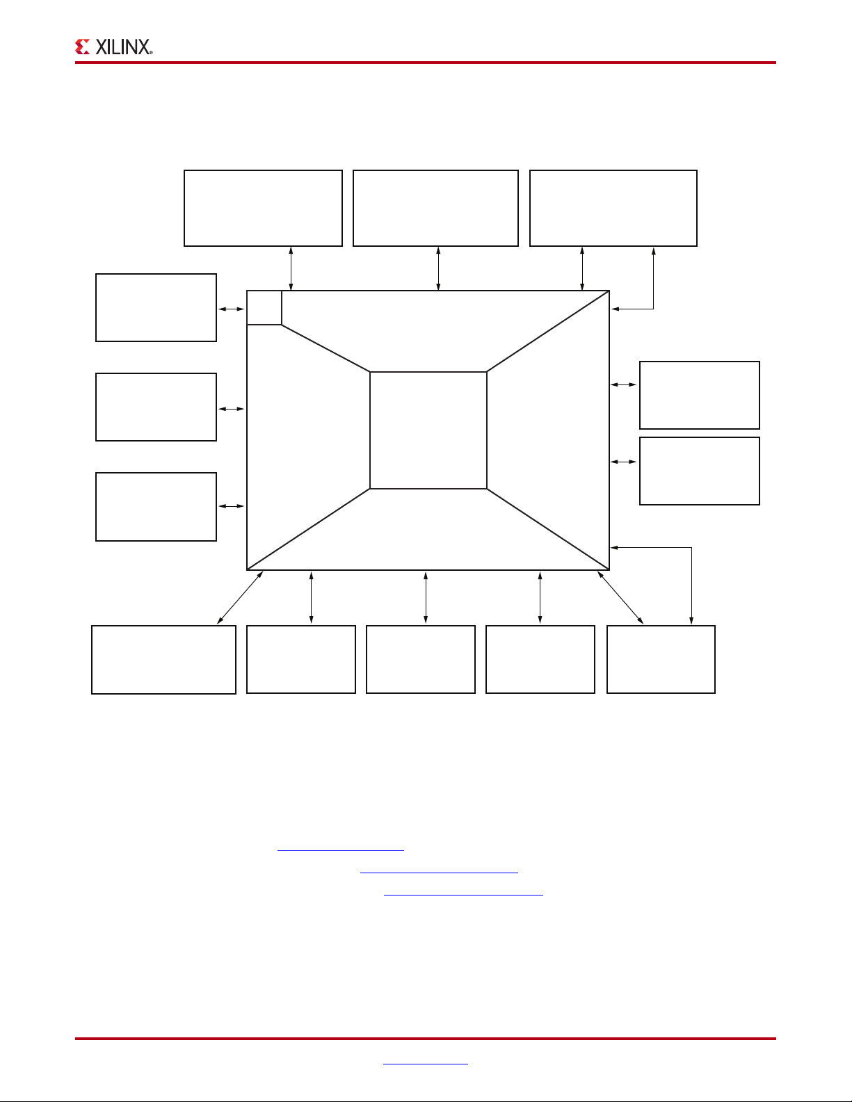
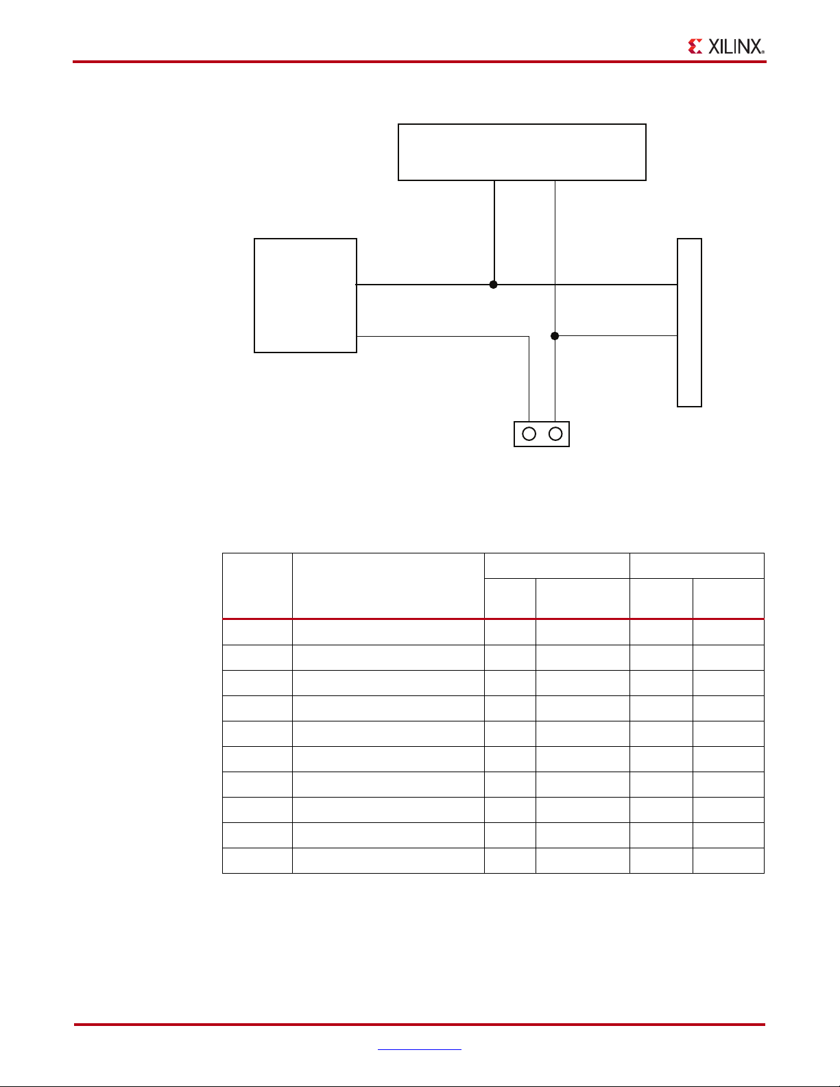
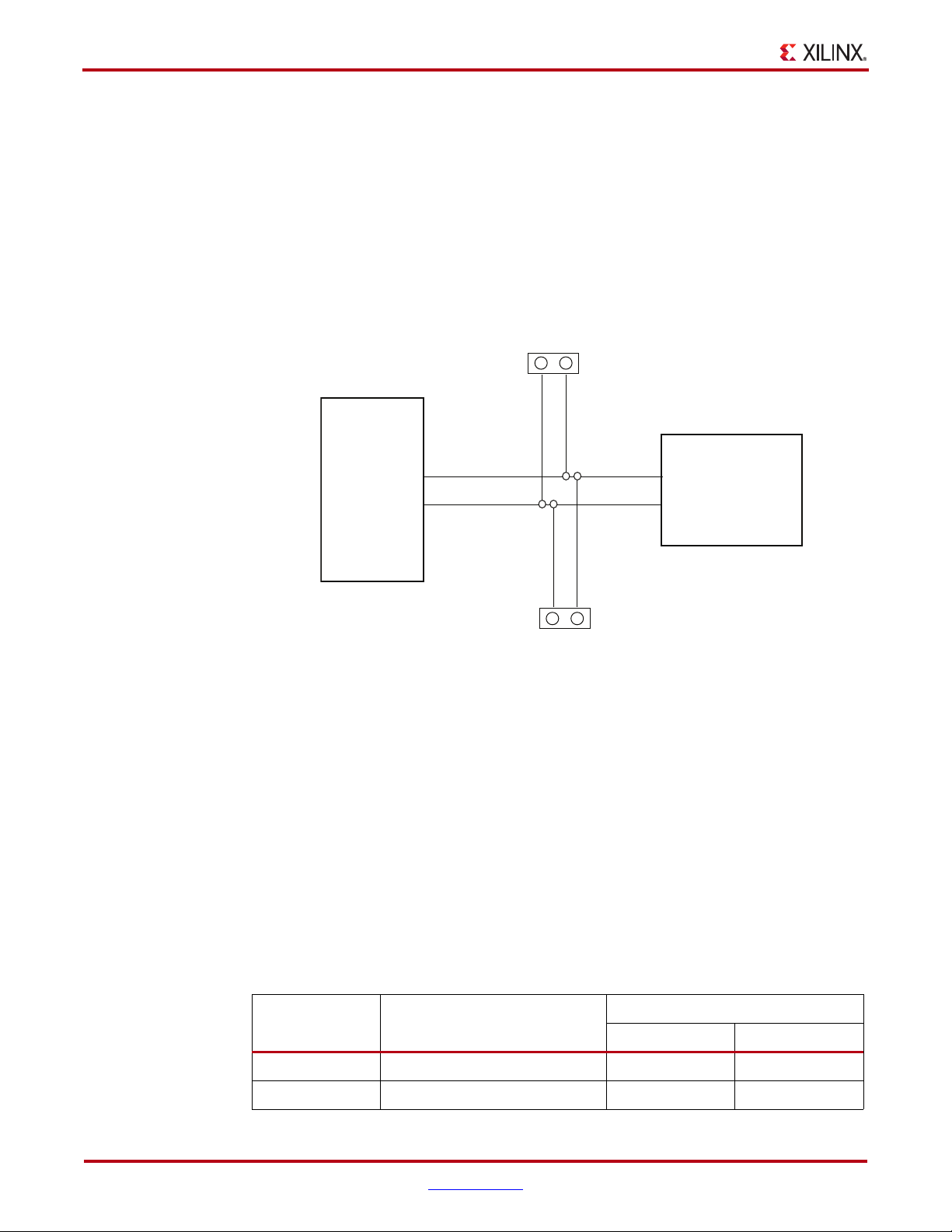
X-Ref Target - Figure 1-1
Related Xilinx Documents
Block Diagram
Figure 1-1 shows a high-level block diagram of the SP601 and its peripherals.
USB
JTAG Connector
DDR2
Pushbuttons
LEDs
DIP Switch
GPIO Header
DED
Bank 3
1.8V
Part of
FMC LPC
Expansion Connector
Bank 0
2.5 V
Spartan-6
XC6SLX16
U1
Bank 2
2.5V
10/100/1000
Ethernet GMII
Parallel Flash
Bank 1
2.5V
Differential Clock
Clock Socket
SMA Clock
Part of
FMC LPC
Expansion Connector
IIC EEPROM
and Header
Figure 1-1: SP601 Features and Banking
Related Xilinx Documents
Prior to using the SP601 Evaluation Board, users should be familiar with Xilinx resources.
See the following locations for additional documentation on Xilinx tools and solutions:
•ISE: www.xilinx.com/ise
• Answer Browser: www.xilinx.com/support
• Intellectual Property: www.xilinx.com/ipcenter
MODE
DIP Switch
SPI x4 or
External Config
USB UART
UG518_01_090909
SP601 Hardware User Guide www.xilinx.com 9
UG518 (v1.7) September 26, 2012
Page 10
Chapter 1: SP601 Evaluation Board
UG518_02_091009
12
8
4
3
12
6
13
7 11
5
10
9
14
15
8
13
16
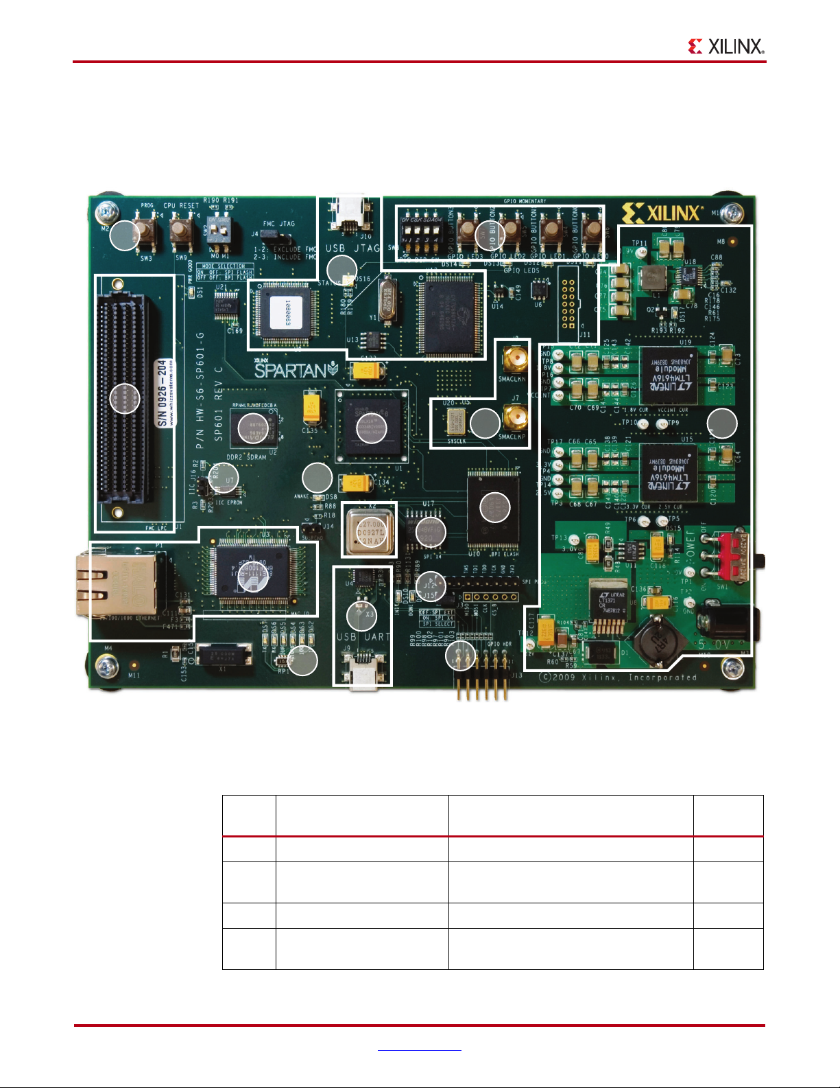
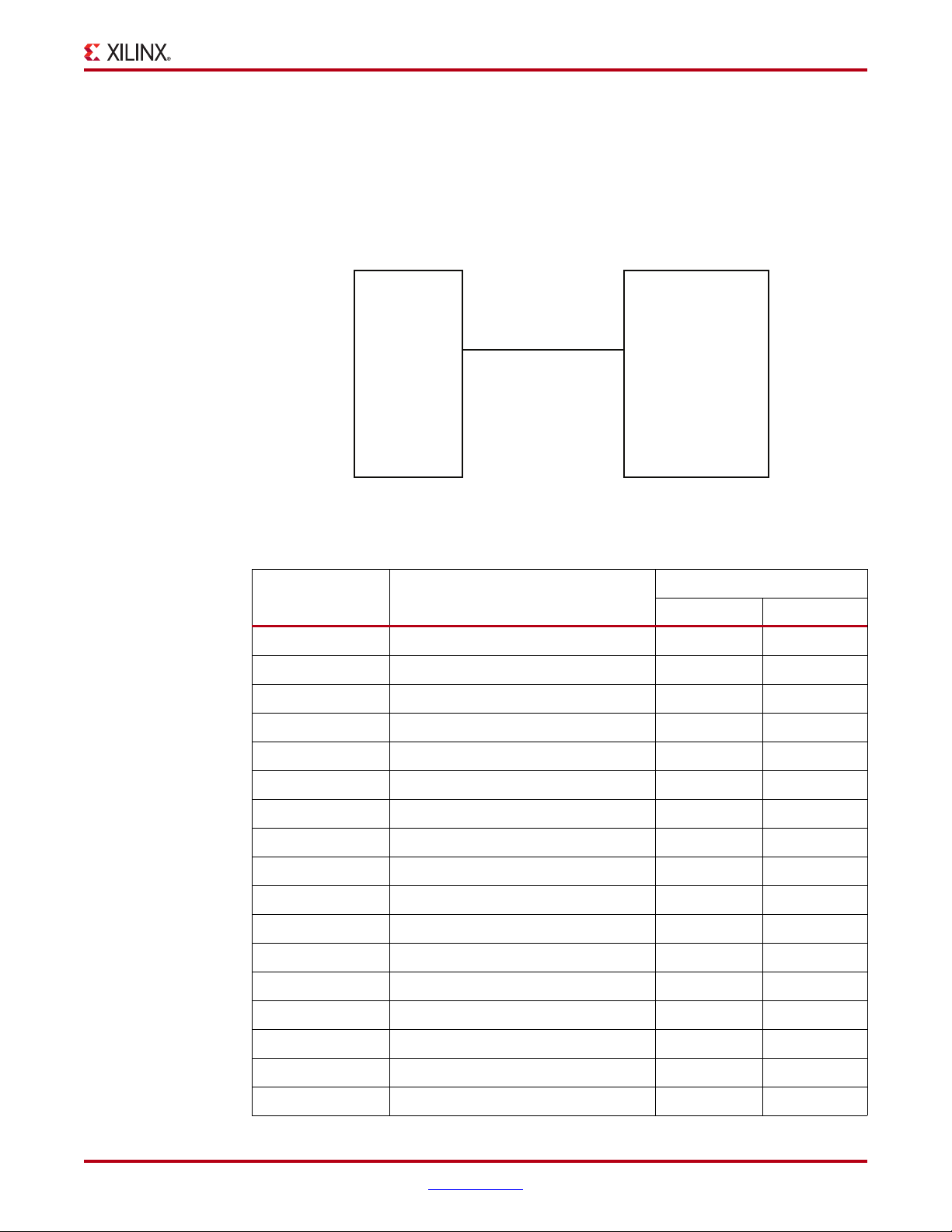
Detailed Description
Figure 1-2 shows a board photo with numbered features corresponding to Tab le 1 -1 and
the section headings in this document.
X-Ref Target - Figure 1-2
The numbered features in Figure 1-2 correlate to the features and notes listed in Ta bl e 1 -1 .
Table 1-1: SP601 Features
Number Feature Notes
Figure 1-2: SP601 Board Photo
1 Spartan-6 FPGA XC6SLX16-2CSG324
2 DDR2 Component Elpida EDE1116ACBG 1 Gb
3 SPI x4 Flash and Headers SPI select and External Headers 8
4 Linear Flash BPI StrataFlash 8-bit (J3 device), 3 pins
DDR2 SDRAM
shared w/ SPI x4
Schematic
Page
5
8
10 www.xilinx.com SP601 Hardware User Guide
UG518 (v1.7) September 26, 2012
Page 11
Table 1-1: SP601 Features (Cont’d)
Detailed Description
Number Feature Notes
5 10/100/1000 Ethernet PHY GMII Marvell Alaska PHY 7
6 RS232 UART (USB Bridge) Uses CP2103 Serial-to-USB connection 10
7 IIC Goes to Header and VITA 57.1 FMC 10
8 Clock, socket, SMA Differential, Single-Ended, Differential 9
9 VITA 57.1 FMC-LPC
connector
10 LEDs Ethernet PHY Status 7
11 LED, Header FPGA Awake LED, Suspend Header 8
12 LEDs FPGA INIT, DONE 9
LED User I/O (active-High) 9
DIP Switch User I/O (active-High) 9
13
Pushbutton User I/O, CPU_RESET (active-High) 9
12-pin (8 I/O) Header 6 pins x 2 male header with 8 I/Os
14 Pushbutton FPGA_PROG_B 9
LVDS signals, clocks, PRSNT 6
(active-High)
Schematic
Page
10
15 USB JTAG Cypress USB to JTAG download cable
logic
16 Onboard Power Power Management 11,12,13
1. Spartan-6 XC6SLX16-2CSG324 FPGA
A Xilinx Spartan-6 XC6SLX16-2CSG324 FPGA is installed on the SP601 Evaluation Board.
References
See the Spartan-6 FPGA Data Sheet. [Ref 1]
Configuration
The SP601 supports configuration in the following modes:
•Master SPI x4
• Master SPI x4 with off-board device
•BPI
•JTAG (using the included USB-A to Mini-B cable)
For details on configuring the FPGA, see 15. Configuration Options.
The Mode DIP switch SW2 is set to M[1:0] = 01 Master SPI default.
14, 15
References
See the Spartan-6 FPGA Configuration User Guide for more information. [Ref 2]
SP601 Hardware User Guide www.xilinx.com 11
UG518 (v1.7) September 26, 2012
Page 12
Chapter 1: SP601 Evaluation Board
I/O Voltage Rails
There are four available banks on the LX16-CSG324 device. Banks 0, 1, and 2 are connected
for 2.5V I/O. Bank 3 is used for the 1.8V DDR2 component memory interface of Spartan-6
FPGA’s hard memory controller. The voltage applied to the FPGA I/O banks used by the
SP601 board is summarized in Tab le 1 -2 .
Table 1-2: I/O Voltage Rail of FPGA Banks
FPGA Bank I/O Voltage Rail
References
See the Spartan-6 FPGA documentation for more information at
http://www.xilinx.com/support/documentation/
02.5V
12.5V
22.5V
31.8V
spartan-6.htm.
2. 128 MB DDR2 Component Memory
There are 128 MB of DDR2 memory available on the SP601 board. A 1-Gb Elpida
EDE1116ACBG (84-ball) DDR2 memory component is accessible through Bank 3 of the
LX16 device. The Spartan-6 FPGA hard memory controller is used for data transfer across
the DDR2 memory interface’s 16-bit data path using SSTL18 signaling. The SP601 board
supports the “standard” VCCINT setting of 1.20V ± 5%. This setting provides the standard
memory controller block (MCB) performance of 625 Mb/s for DDR2 memory in a -2 speed
grade device. Signal integrity is maintained through DDR2 resistor terminations and
memory on-die terminations (ODT), as shown in Ta bl e 1 - 3 and Ta bl e 1 -4 .
Table 1-3: Termination Resistor Requirements
Signal Name Board Termination On-Die Termination
DDR2_A[14:0] 49.9Ω to V
DDR2_BA[2:0] 49.9Ω to V
DDR2_RAS_N 49.9Ω to V
DDR2_CAS_N 49.9Ω to V
DDR2_WE_N 49.9Ω to V
DDR2_CS_N 100Ω to GND
DDR2_CKE 4.7KΩ to GND
DDR2_ODT 4.7KΩ to GND
TT
TT
TT
TT
TT
DDR2_DQ[15:0] ODT
DDR2_UDQS[P,N],
DDR2_LDQS[P,N]
DDR2_UDM, DDR2_LDM ODT
12 www.xilinx.com SP601 Hardware User Guide
UG518 (v1.7) September 26, 2012
ODT
Page 13
Table 1-3: Termination Resistor Requirements (Cont’d)
Signal Name Board Termination On-Die Termination
Detailed Description
DDR2_CK[P,N]
Notes:
1. Nominal value of VTT for DDR2 interface is 0.9V.
100Ω differential at memory
component
Table 1-4: FPGA On-Chip (OCT) Termination External Resistor Requirements
FPGA U1 Pin FPGA Pin Number Board Connection for OCT
ZIO L6 No Connect
RZQ C2 100Ω to GROUND
Tab le 1 -5 shows the connections and pin numbers for the DDR2 Component Memory.
Table 1-5: DDR2 Component Memory Connections
FPGA U1
Pin
Schematic Net Name
Pin Number Pin Name
Memory U2
J7 DDR2_A0 M8 A0
J6 DDR2_A1 M3 A1
H5 DDR2_A2 M7 A2
L7 DDR2_A3 N2 A3
F3 DDR2_A4 N8 A4
H4 DDR2_A5 N3 A5
H3 DDR2_A6 N7 A6
H6 DDR2_A7 P2 A7
D2 DDR2_A8 P8 A8
D1 DDR2_A9 P3 A9
F4 DDR2_A10 M2 A10
D3 DDR2_A11 P7 A11
G6 DDR2_A12 R2 A12
L2 DDR2_DQ0 G8 DQ0
L1 DDR2_DQ1 G2 DQ1
K2 DDR2_DQ2 H7 DQ2
K1 DDR2_DQ3 H3 DQ3
H2 DDR2_DQ4 H1 DQ4
H1 DDR2_DQ5 H9 DQ5
J3 DDR2_DQ6 F1 DQ6
SP601 Hardware User Guide www.xilinx.com 13
UG518 (v1.7) September 26, 2012
Page 14
Chapter 1: SP601 Evaluation Board
Table 1-5: DDR2 Component Memory Connections (Cont’d)
FPGA U1
Pin
J1 DDR2_DQ7 F9 DQ7
M3 DDR2_DQ8 C8 DQ8
M1 DDR2_DQ9 C2 DQ9
N2 DDR2_DQ10 D7 DQ10
N1 DDR2_DQ11 D3 DQ11
T2 DDR2_DQ12 D1 DQ12
T1 DDR2_DQ13 D9 DQ13
U2 DDR2_DQ14 B1 DQ14
U1 DDR2_DQ15 B9 DQ15
F2 DDR2_BA0 L2 BA0
F1 DDR2_BA1 L3 BA1
E1 DDR2_BA2 L1 BA2
Schematic Net Name
Pin Number Pin Name
Memory U2
E3 DDR2_WE_B K3 WE
L5 DDR2_RAS_B K7 RAS
K5 DDR2_CAS_B L7 CAS
K6 DDR2_ODT K9 ODT
G3 DDR2_CLK_P J8 CK
G1 DDR2_CLK_N K8 CK
H7 DDR2_CKE K2 CKE
L4 DDR2_LDQS_P F7 LDQS
L3 DDR2_LDQS_N E8 LDQS
P2 DDR2_UDQS_P B7 UDQS
P1 DDR2_UDQS_N A8 UDQS
K3 DDR2_LDM F3 LDM
K4 DDR2_UDM B3 UDM
References
See the Elpida DDR2 SDRAM Specifications for more information. [Ref 11]
Also, see the
Spartan-6 FPGA Memory Controller User Guide. [Ref 3]
14 www.xilinx.com SP601 Hardware User Guide
UG518 (v1.7) September 26, 2012
Page 15
3. SPI x4 Flash
SPI Prog
FPGA_D1_MISO2
J12
1
2
3
4
5
6
7
8
9
FPGA_D2_MISO3
FPGA_PROG_B
FPGA_MOSI_CSI_B_MISO0
SPI_CS_B
FPGA_CCLK
FPGA_D0_DIN_MISO_MISO1
UG518_04_040910
GND
VCC3V3
Silkscreen
TMS
TDI
TDO
TCK
GND
3V3
HDR_1X9
The Xilinx Spartan-6 FPGA hosts a SPI interface which is accessible to the Xilinx iMPACT
configuration tool. The SPI memory device operates at 3.0V; the Spartan-6 FPGA I/Os are
3.3V tolerant and provide electrically compatible logic levels to directly access the SPI flash
through a 2.5V bank. The XC6SLX16-2CSG324 is a master device when accessing an
external SPI flash memory device.
The SP601 SPI interface has two parallel connected configuration options (see Figure 1-4):
an SPI X4 (Winbond W25Q64VSFIG) 64-Mb flash memory device and a flash
programming header (J12). J12 supports a user-defined SPI mezzanine board. The SPI
configuration source is selected via SPI select jumper J15. For details on configuring the
FPGA, see 15. Configuration Options.
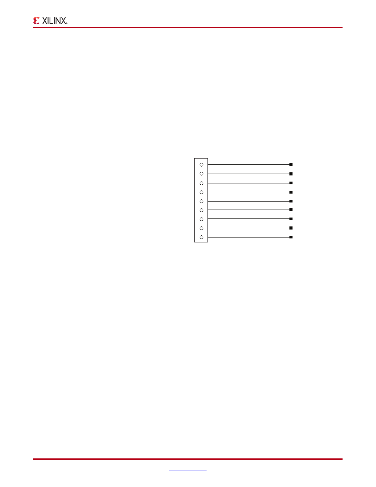
X-Ref Target - Figure 1-3
Detailed Description
Figure 1-3: J12 SPI Flash Programming Header
SP601 Hardware User Guide www.xilinx.com 15
UG518 (v1.7) September 26, 2012
Page 16
Chapter 1: SP601 Evaluation Board
U1
FPGA SPI INTERFACE
U17
J12
SPI X4
FLASH
MEMORY
WINBOND
W25Q64VSFIG
SPI PROGRAM
HEADER
SPI SELECT
JUMPER
ON = SPI X4 U17
OFF = SPI EXT. J12
SPIX4_CS_B
DIN,DOUT,CCLK
SPI_CS_B
2
J15
1
UG518_07_070809
X-Ref Target - Figure 1-4
Figure 1-4: SPI Flash Interface Topology
Table 1-6: SPI x4 Memory Connections
FPGA U1
Pin
V2 FPGA_PROG_B 1
V14 FPGA_D2_MISO3 1 IO3_HOLD_B 2
T14 FPGA_D1_MISO2_R 9 IO2_WP_B 3
V3 SPI_CS_B 4 TMS
T13 FPGA_MOSI_CSI_B_MISO0 15 DIN 5 TDI
R13 FPGA_D0_DIN_MISO_MISO1 8 IO1_DOUT 6 TDO
R15 FPGA_CCLK 16 CLK 7 TCK
Schematic Net Name
SPI MEM U17 SPI HDR J12
Pin # Pin Name
Pin
Number
8GND
9 VCC3V3
J15.2 SPIX4_CS_B 7 CS_B
References
Pin Name
16 www.xilinx.com SP601 Hardware User Guide
See the Winbond Serial Flash Memory Data Sheet for more information. [Ref 12]
See the XPS Serial Peripheral Interface Data Sheet for more information. [Ref 4]
UG518 (v1.7) September 26, 2012
Page 17
4. Linear Flash BPI
An 8-bit (16 MB) Numonyx linear flash memory (TE28F128J3D-75) (J3D type) is used to
provide non-volatile bitstream, code, and data storage. The J3D devices operate at 3.0V; the
Spartan-6 FPGA I/Os are 3.3V tolerant and provide electrically compatible logic levels to
directly access the linear flash BPI through a 2.5V bank. For details on configuring the
FPGA, see 15. Configuration Options.
X-Ref Target - Figure 1-5
Detailed Description
U1 U10
FPGA
BPI FLASH
INTERFACE
ADDR, DATA, CTRL
Figure 1-5: Linear Flash BPI Interface
Table 1-7: BPI Memory Connections
FPGA U1 Pin Schematic Net Name
K18 FLASH_A0 32 A0
K17 FLASH_A1 28 A1
J18 FLASH_A2 27 A2
J16 FLASH_A3 26 A3
G18 FLASH_A4 25 A4
G16 FLASH_A5 24 A5
NUMONYX TYPE J3vD
T28F128J3D-75
UG518_09_070809
BPI Memory U10
Pin Number Pin Name
H16 FLASH_A6 23 A6
H15 FLASH_A7 22 A7
H14 FLASH_A8 20 A8
H13 FLASH_A9 19 A9
F18 FLASH_A10 18 A10
F17 FLASH_A11 17 A11
K13 FLASH_A12 13 A12
K12 FLASH_A13 12 A13
E18 FLASH_A14 11 A14
E16 FLASH_A15 10 A15
G13 FLASH_A16 8 A16
SP601 Hardware User Guide www.xilinx.com 17
UG518 (v1.7) September 26, 2012
Page 18
Chapter 1: SP601 Evaluation Board
Table 1-7: BPI Memory Connections (Cont’d)
FPGA U1 Pin Schematic Net Name
H12 FLASH_A17 7 A17
D18 FLASH_A18 6 A18
D17 FLASH_A19 5 A19
G14 FLASH_A20 4 A20
F14 FLASH_A21 3 A21
C18 FLASH_A22 1 A22
C17 FLASH_A23 30 A23
F16 FLASH_A24 56 A24
R13 FPGA_D0_DIN_MISO_MISO1 33 DQ0
T14 FPGA_D1_MISO2 35 DQ1
V14 FPGA_D2_MISO3 38 DQ2
U5 FLASH_D3 40 DQ3
V5 FLASH_D4 44 DQ4
BPI Memory U10
Pin Number Pin Name
R3 FLASH_D5 46 DQ5
T3 FLASH_D6 49 DQ6
R5 FLASH_D7 51 DQ7
M16 FLASH_WE_B 55 WE_B
L18 FLASH_OE_B 54 OE_B
L17 FLASH_CE_B 14 CE0
B3 FMC_PWR_GOOD_FLASH_RST_B 16 RP_B
Note: Memory U10 pin 56 address A24 is not connected on the 16 MB device. It is made available
for larger density devices.
References
See the Numonyx Embedded Flash Memory Data Sheet for more information. [Ref 13]
In addition, see the Spartan-6 FPGA Configuration User Guide for more information. [Ref 2]
18 www.xilinx.com SP601 Hardware User Guide
UG518 (v1.7) September 26, 2012
Page 19

5. 10/100/1000 Tri-Speed Ethernet PHY
The SP601 uses the onboard Marvell Alaska PHY device (88E1111) for Ethernet
communications at 10, 100, or 1000 Mb/s. The board supports a GMII/MII interface from
the FPGA to the PHY. The PHY connection to a user-provided Ethernet cable is through a
Halo HFJ11-1G01E RJ-45 connector with built-in magnetics.
On power-up, or on reset, the PHY is configured to operate in GMII mode with PHY
address 0b00111 using the settings shown in Tab le 1 -8 . These settings can be overwritten
via software commands passed over the MDIO interface.
Table 1-8: PHY Configuration Pins
Detailed Description
Connection on
Pin
CFG0 V
Board
2.5V PHYADR[2] = 1 PHYADR[1] = 1 PHYADR[0] = 1
CC
Definition and Value
Bit[2]
Bit[1]
Definition and Value
Bit[0]
Definition and Value
CFG1 Ground ENA_PAUSE = 0 PHYADR[4] = 0 PHYADR[3] = 0
CFG2 V
CFG3 V
CFG4 V
CFG5 V
2.5V ANEG[3] = 1 ANEG[2] = 1 ANEG[1] = 1
CC
2.5V ANEG[0] = 1 ENA_XC = 1 DIS_125 = 1
CC
2.5V HWCFG_MD[2] = 1 HWCFG_MD[1] = 1 HWCFG_MD[0] = 1
CC
2.5V DIS_FC = 1 DIS_SLEEP = 1 HWCFG_MD[3] = 1
CC
CFG6 PHY_LED_RX SEL_BDT = 0 INT_POL = 1 75/50Ω = 0
Table 1-9: Ethernet PHY Connections
U3 M88E111
FPGA U1 Pin Schematic Net Name
Pin Number Pin Name
P16 PHY_MDIO 33 MDIO
N14 PHY_MDC 35 MDC
J13 PHY_INT 32 INT_B
L13 PHY_RESET 36 RESET_B
M13 PHY_CRS 115 CRS
L14 PHY_COL 114 COL
L16 PHY_RXCLK 7 RXCLK
P17 PHY_RXER 8 RXER
N18 PHY_RXCTL_RXDV 4 RXDV
M14 PHY_RXD0 3 RXD0
U18 PHY_RXD1 128 RXD1
U17 PHY_RXD2 126 RXD2
T18 PHY_RXD3 125 RXD3
T17 PHY_RXD4 124 RXD4
N16 PHY_RXD5 123 RXD5
SP601 Hardware User Guide www.xilinx.com 19
UG518 (v1.7) September 26, 2012
Page 20
Chapter 1: SP601 Evaluation Board
Table 1-9: Ethernet PHY Connections (Cont’d)
FPGA U1 Pin Schematic Net Name
U3 M88E111
Pin Number Pin Name
N15 PHY_RXD6 121 RXD6
P18 PHY_RXD7 120 RXD7
A9 PHY_TXC_GTPCLK 14 GTXCLK
B9 PHY_TXCLK 10 TXCLK
A8 PHY_TXER 13 TXER
B8 PHY_TXCTL_TXEN 16 TXEN
F8 PHY_TXD0 18 TXD0
G8 PHY_TXD1 19 TXD1
A6 PHY_TXD2 20 TXD2
B6 PHY_TXD3 24 TXD3
E6 PHY_TXD4 25 TXD4
F7 PHY_TXD5 26 TXD5
A5 PHY_TXD6 28 TXD6
C5 PHY_TXD7 29 TXD7
References
See the Marvell Alaska Gigabit Ethernet Transceivers product page for more information.
[Ref 16]
Also, see the LogiCORE™ IP Tri-Mode Ethernet MAC User Guide. [Ref 5]
20 www.xilinx.com SP601 Hardware User Guide
UG518 (v1.7) September 26, 2012
Page 21

6. USB-to-UART Bridge
The SP601 contains a Silicon Labs CP2103GM USB-to-UART bridge device (U4) which
allows connection to a host computer with a USB cable. The USB cable is supplied in this
evaluation kit (Type A end to host computer, Type Mini-B end to SP601 connector J9).
Tab le 1 -10 details the SP601 J9 pinout.
Xilinx UART IP is expected to be implemented in the FPGA fabric. The FPGA supports the
USB-to-UART bridge using four signal pins, transmit (TX), receive (RX), Request to Send
(RTS), and Clear to Send (CTS).
Silicon Labs provides royalty-free Virtual COM Port (VCP) drivers which permit the
CP2103GM USB-to-UART bridge to appear as a COM port to host computer
communications application software (for example, HyperTerm or TeraTerm). The VCP
device driver must be installed on the host PC prior to establishing communications with
the SP601. Refer to the SP601 Getting Started Guide for driver installation instructions.
Table 1-10: USB Type B Pin Assignments and Signal Definitions
Detailed Description
USB Connector
Pin
1 VBUS +5V from host system (not used)
2 USB_DATA_N Bidirectional differential serial data (N-side)
3 USB_DATA_P Bidirectional differential serial data (P-side)
4 GROUND Signal ground
Signal Name Description
Table 1-11: CP2103GM Connections
FPGA U1 Pin
U10 RTS, output USB_1_CTS 22 CTS, input
T5 CTS, input USB_1_RTS 23 RTS, output
L12 TX, data out USB_1_RX 24 RXD, data in
K14 RX, data in USB_1_TX 25 TXD, data out
UART Function
in FPGA
Schematic
Net Name
U4 CP2103GM
Pin
UART Function
in CP2103GM
References
Refer to the Silicon Labs website for technical information on the CP2103GM and the VCP
drivers.
In addition, see some of the Xilinx UART IP specifications at:
• http://www.xilinx.com/support/documentation/ip_documentation/xps_uartlite.pdf
• http:
SP601 Hardware User Guide www.xilinx.com 21
UG518 (v1.7) September 26, 2012
//
www.xilinx.com/support/documentation/ip_documentation/xps_uart16550.pdf
Page 22
Chapter 1: SP601 Evaluation Board
FPGA IIC
INTERFACE
U1
IIC_SDA_MAIN
IIC_SCL_MAIN
2
C30 C31
1
J16
J1
IIC EXTERNAL
ACCESS
CONNECTOR
VITA 57.1
FMC-LPC
U7
ST MICRO
M24 C08-WDW6TP
UG518_13_070809
Address range
54-56
0b1010100-
0b1010110
FMC-LPC
GA0=1
GA1=0
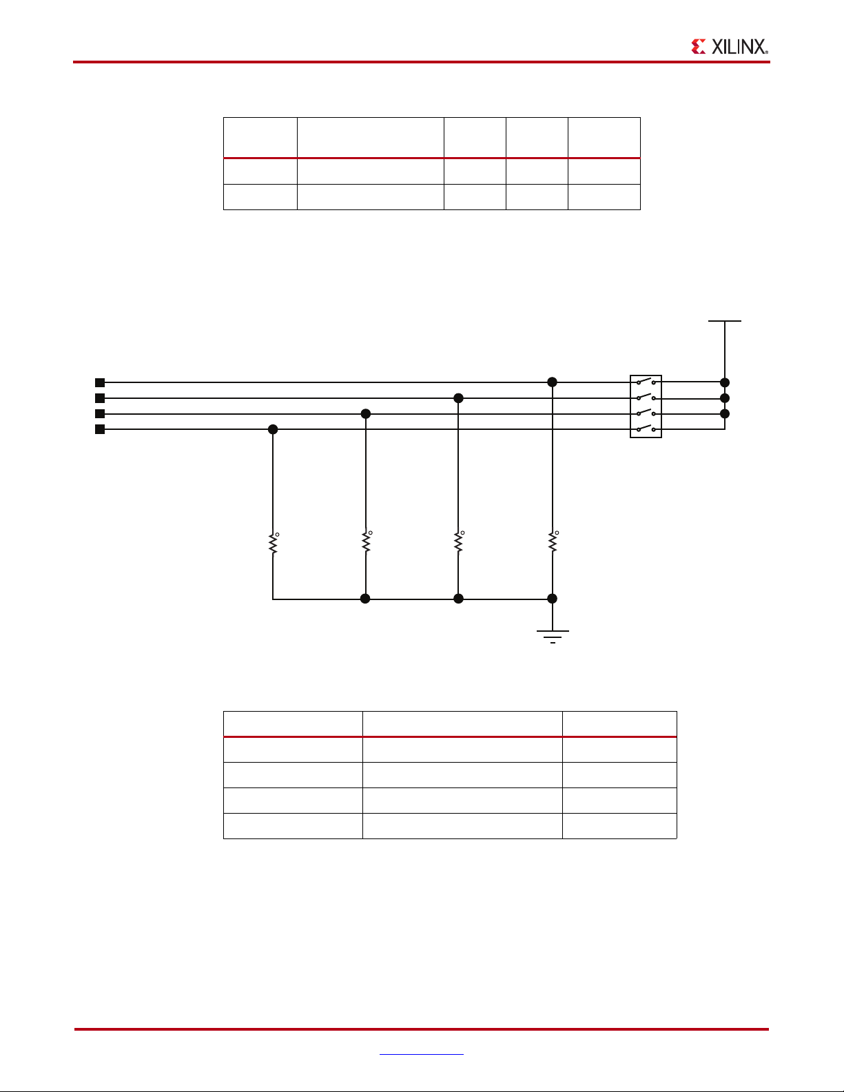
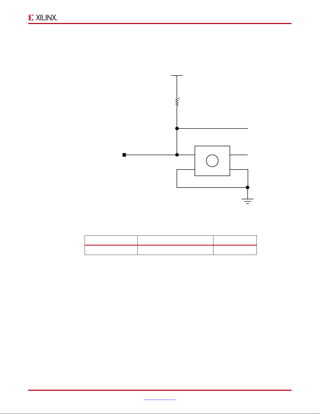
7. IIC Bus
The SP601 IIC bus hosts four items:
• FPGA U1 IIC interface
• 2-pin IIC external access header
•8-Kb NV Memory
• VITA 57.1 FMC Connector J1
The SP601 IIC bus topology is shown in Figure 1-6.
X-Ref Target - Figure 1-6
Figure 1-6: IIC Bus Topology
The IIC Bus on the SP601 provides access to a 2-pin header, the onboard 8-Kb EEPROM,
and the VITA 57.1 FMC interface. The user must ensure there are no IIC address conflicts
with the onboard EEPROM address when attaching additional IIC devices via FMC or the
IIC 2-pin header. Note that FMC Mezzanine cards are designed with 2-Kb IIC EEPROMs
and will not conflict with the Carrier Card (SP601) 8-Kb EEPROM address range. This is
because 2-Kb EEPROMs reside below the 8-Kb EEPROM space. See the VITA 57.1
specification along with any IIC 2-Kbit EEPROM data sheet for more details.
8-Kb NV Memory
The SP601 hosts a 8-Kb ST Microelectronics M24C08-WDW6TP IIC parameter storage
memory device (U7). The IIC address of U7 is 0b1010100, and U7 is not write protected
(WP pin 7 is tied to GND).
Table 1-12: IIC Memory Connections
FPGA U1 Pin Schematic Net Name
Not Applicable Tied to GND 1 A0
Not Applicable Tied to GND 2 A1
22 www.xilinx.com SP601 Hardware User Guide
SPI Memory U7
Pin Number Pin Name
UG518 (v1.7) September 26, 2012
Page 23

Table 1-12: IIC Memory Connections (Cont’d)
Detailed Description
FPGA U1 Pin Schematic Net Name
Not Applicable Pulled up (0Ω) to VCC3V3 3 A2
N10 IIC_SDA_MAIN 5 SDA
P11 IIC_SCL_MAIN 6 SCL
Not Applicable Tied to GND 7 WP
References
See the ST Micro M24C08 Data Sheet for more information. [Ref 17]
In addition, see the Xilinx XPS IIC Bus Interface Data Sheet. [Ref 6]
Also, see 9. VITA 57.1 FMC-LPC Connector, page 25.
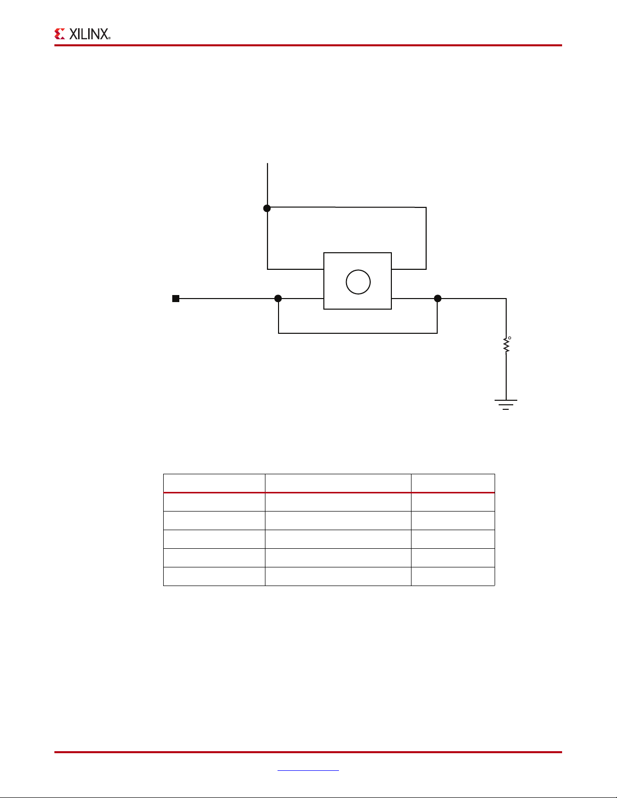
8. Clock Generation
There are three clock sources available on the SP601.
Oscillator (Differential)
The SP601 has one 2.5V LVDS differential 200 MHz oscillator (U5) soldered onto the board
and wired to an FPGA global clock input.
SPI Memory U7
Pin Number Pin Name
• Crystal oscillator: SiTime SiT9102AI-243N25E200.00000
• PPM frequency stability: 50 ppm
References
See the SiTime SiT9102 Data Sheet for more information. [Ref 14]
SP601 Hardware User Guide www.xilinx.com 23
UG518 (v1.7) September 26, 2012
Page 24
Chapter 1: SP601 Evaluation Board
O
scillator top has
corner dot marking
UG518_06_091009
Oscillator body has
one square corner
Oscillator Socket (Single-Ended, 2.5V or 3.3V)
One populated single-ended clock socket (X2) is provided for user applications. The option
of 3.3V or 2.5V power may be selected via a 0Ω resistor selection. The SP601 board is
shipped with a 27 MHz 2.5V oscillator installed.
Figure 1-7 shows the unpopulated user oscillator socket, indicating the socket pin 1
location. Figure 1-8 shows the oscillator installed, indicating its pin 1 location.
X-Ref Target - Figure 1-7
X-Ref Target - Figure 1-8
Socket has notch
in crossbar
Silkscreened outline
has beveled corner
UG518_05_101409
Figure 1-7: SP601 Oscillator Socket Pin 1 Location Identifiers
24 www.xilinx.com SP601 Hardware User Guide
Figure 1-8: SP601 Oscillator Pin 1 Location Identifiers
SMA Connectors (Differential)
A high-precision clock signal can be provided to the FPGA using differential clock signals
through the onboard 50Ω SMA connectors J8 (N) and J7 (P).
Table 1-13: SP601 Clock Source Connections
Source FPGA U1 Pin Schematic Net Name Pin Number Pin Name
K16 SYSCLK_N 5 OUT_B
U5 200 MHz OSC
K15 SYSCLK_P 4 OUT
X2 27 MHz OSC V10 USER_CLOCK 5 OUT
USER_SMA_CLOCK H18 SMACLK_N J8.1 -
SMA Connectors H17 SMACLK_P J7.1 -
UG518 (v1.7) September 26, 2012
Page 25
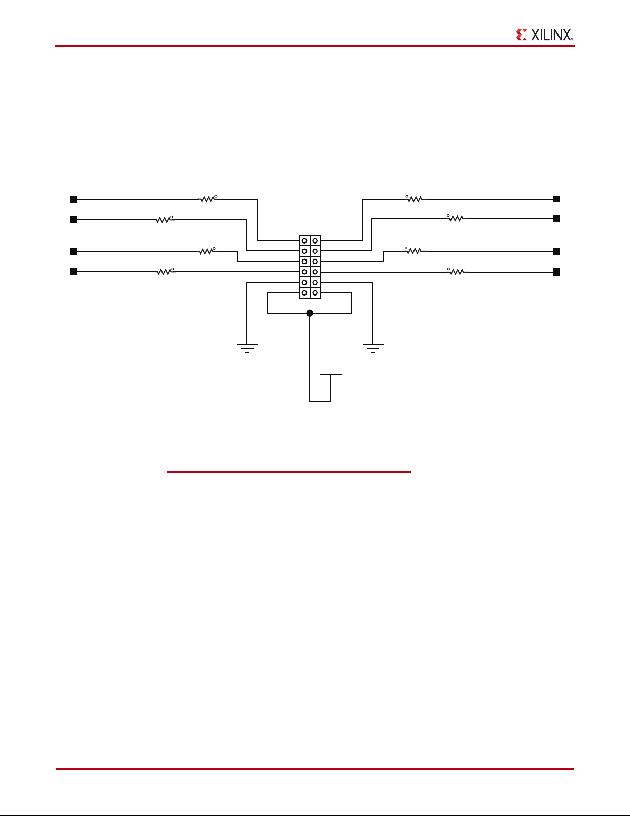
9. VITA 57.1 FMC-LPC Connector
The VITA 57.1 FMC expansion connector (J1) on the SP601 implements the VITA 57.1.1 LPC
format of the VITA 57.1 FMC standard specification. The VITA 57.1 FMC-LPC connector
provides 68 single-ended (34 differential) user-defined signals. The VITA 57.1 FMC
standard calls for two connector densities: a High Pin Count (HPC) and a Low Pin Count
(LPC) implementation. A common 10 x 40 position (400 pin locations) connector form
factor is used for both versions. The HPC version has 400 pins present, the LPC version,
160 pins. The Samtec connector system is rated for signaling speeds up to 9 GHz (18 Gb/s)
based on a -3dB insertion loss point within a two-level signaling environment. Refer to the
Samtec website
VITA 57.1 FMC-LPC connector (ASP-134603-01) and its mate.
for data sheets and characterization information for the RoHS-compliant
Detailed Description
Note:
adjustable). The 2.5V rail cannot be turned off. The FMC LPC J1 connector is a keyed connector
oriented so that a plug-on card faces away from the SP601 board. The SP601 VITA 57.1 FMC
interface is compatible with 2.5V mezzanine cards capable of supporting 2.5V VADJ.
The SP601 board VADJ voltage for the FMC LPC connector (J1) is fixed at 2.5V (non-
Tab le 1 -14 shows the VITA 57.1 FMC LPC connections. The connector pinout is in
Appendix B, VITA 57.1 FMC LPC Connector Pinout.
Any signal named FMC_HPC_xxxx that is wired between a U1 FPGA pin and some other
device does not appear in this table.
The SP601 supports all FMC LA Bus connections available on the FMC LPC connector,
(LA[00:33]) along with all available FMC M2C clock pairs (CLK0_M2C_P/N and
CLK1_M2C_P/N). The SP601 does not support the FMC DP Bus connections since the
SP601 does not support any Gigabit Transceivers on the FMC DP Bus. Therefore,
DP0_C2M_P/N, DP0_M2C_P/N and GBTCLK0_M2C_P/N are not supported by the
SP601 FMC interface.
For more details about FMC, see the VITA57.1 specification available at
http://www.vita.com/fmc.html
.
Table 1-14: VITA 57.1 FMC LPC Connections
J1 FMC
LPC Pin
C10 FMC_LA06_P D12 D1 FMC_PWR_GOOD_FLASH_RST_B B3
C11 FMC_LA06_N C12 D8 FMC_LA01_CC_P D11
Schematic Net Name
U1 FPGA
Pin
J1 FMC
LPC Pin
Schematic Net Name
U1 FPGA
Pin
C14 FMC_LA10_P D8 D9 FMC_LA01_CC_N C11
C15 FMC_LA10_N C8 D11 FMC_LA05_P B14
C18 FMC_LA14_P B2 D12 FMC_LA05_N A14
C19 FMC_LA14_N A2 D14 FMC_LA09_P G11
C22 FMC_LA18_CC_P R10 D15 FMC_LA09_N F10
C23 FMC_LA18_CC_N T10 D17 FMC_LA13_P B11
C26 FMC_LA27_P R11 D18 FMC_LA13_N A11
C27 FMC_LA27_N T11 D20 FMC_LA17_CC_P R8
C30 IIC_SCL_MAIN P11 D21 FMC_LA17_CC_N T8
C31 IIC_SDA_MAIN N10 D23 FMC_LA23_P N5
SP601 Hardware User Guide www.xilinx.com 25
UG518 (v1.7) September 26, 2012
Page 26

Chapter 1: SP601 Evaluation Board
Table 1-14: VITA 57.1 FMC LPC Connections (Cont’d)
J1 FMC
LPC Pin
G2 FMC_CLK1_M2C_P T9 H2 FMC_PRSNT_M2C_L U13
G3 FMC_CLK1_M2C_N V9 H4 FMC_CLK0_M2C_P C10
G6 FMC_LA00_CC_P D9 H5 FMC_CLK0_M2C_N A10
G7 FMC_LA00_CC_N C9 H7 FMC_LA02_P C15
G9 FMC_LA03_P C13 H8 FMC_LA02_N A15
G10 FMC_LA03_N A13 H10 FMC_LA04_P B16
G12 FMC_LA08_P F11 H11 FMC_LA04_N A16
G13 FMC_LA08_N E11 H13 FMC_LA07_P E7
G15 FMC_LA12_P D6 H14 FMC_LA07_N E8
G16 FMC_LA12_N C6 H16 FMC_LA11_P B12
G18 FMC_LA16_P C7 H17 FMC_LA11_N A12
Schematic Net Name
U1 FPGA
Pin
J1 FMC
LPC Pin
D24 FMC_LA23_N P6
D26 FMC_LA26_P U7
D27 FMC_LA26_N V7
Schematic Net Name
U1 FPGA
Pin
G19 FMC_LA16_N A7 H19 FMC_LA15_P G9
G21 FMC_LA20_P N7 H20 FMC_LA15_N F9
G22 FMC_LA20_N P8 H22 FMC_LA19_P N6
G24 FMC_LA22_P R7 H23 FMC_LA19_N P7
G25 FMC_LA22_N T7 H25 FMC_LA21_P T4
G27 FMC_LA25_P M11 H26 FMC_LA21_N V4
G28 FMC_LA25_N N11 H28 FMC_LA24_P U8
G30 FMC_LA29_P M8 H29 FMC_LA24_N V8
G31 FMC_LA29_N N8 H31 FMC_LA28_P U11
G33 FMC_LA31_P T6 H32 FMC_LA28_N V11
G34 FMC_LA31_N V6 H34 FMC_LA30_P T12
G36 FMC_LA33_P M10 H35 FMC_LA30_N V12
G37 FMC_LA33_N N9 H37 FMC_LA32_P U15
H38 FMC_LA32_N V15
26 www.xilinx.com SP601 Hardware User Guide
UG518 (v1.7) September 26, 2012
Page 27

Table 1-15: Power Supply Voltages for LPC Connector
Detailed Description
Voltage Supply Voltage
Number
of Pins
Maximum
Current
Toleran c e
VADJ Fixed 2.5V 2 2A ±5%
VIO_B_M2C NC 0 0A N/A
VREF_A_M2C 0-VADJ 1 0.001A ±2%
VREF_B_M2C NC 0 0A N/A
3P3VAUX 3.3V 1 0.020A ± 5%
3P3V 3.3V 4 3A ±5%
12P0V 12V 2 1A ±5%
SP601 Hardware User Guide www.xilinx.com 27
UG518 (v1.7) September 26, 2012
Page 28

Chapter 1: SP601 Evaluation Board
10. Status LEDs
Tab le 1 -16 defines the status LEDs.
Table 1-16: Status LEDs
Reference
Designator
DS1 FMC_PWR_GOOD_FLASH_RST_B Green
DS2 PHY_LED_LINK10 Green 10 Indicates link speed 10 Mb/s.
DS3 PHY_LED_LINK100 Green 100 Indicates link speed 100 Mb/s.
DS4 PHY_LED_LINK1000 Green 1000 Indicates link speed 1 Gb/s.
DS5 PHY_LED_DUPLEX Green DUP Indicates duplex data.
DS6 PHY_LED_RX Green RX Indicates RX data activity.
DS7 PHY_LED_TX Green TX Indicates TX data activity.
DS8 FPGA_AWAKE Green AWAKE FPGA is not in low-power suspend mode.
DS9 FPGA_DONE Green DONE
DS10 FPGA_INIT Red INIT
DS15 VCC5 Green Illuminates when 5V supply is applied.
Signal Name Color Label Description
PWR
GOOD
Indicates power available for VITA 57.1
FMC expansion connector.
Illuminates to indicate the status of the
DONE pin when the FPGA is successfully
configured.
Illuminates after power-up to indicate that
the FPGA has successfully powered up
and completed its internal power-on
process.
DS16 LED_GRN, LED_RED
DS17 LTC_PWR_GOOD Green
Green/
Red
STATUS USB to JTAG logic.
Illuminates to indicate that the board
power is good.
28 www.xilinx.com SP601 Hardware User Guide
UG518 (v1.7) September 26, 2012
Page 29

X-Ref Target - Figure 1-9
FPGA AWAKE
R88
27.4
1%
1/16W
1
2
LED-GRN-SMT
2
DS8
1
R18
4.7K
5%
1/16W
1
2
J14 Suspend Jumper
OFF = AWAKE (default)
ON = SUSPEND
FPGA SUSPEND
H-1X2
J14
1
2
VCC2V5
UG518_19_070809
Detailed Description
11. FPGA Awake LED and Suspend Jumper
The suspend mode jumper permits the FPGA to enter an inactive, "suspend" mode. The
FPGA Awake LED DS8 will go out when the FPGA enters this mode.
Figure 1-9: FPGA Awake LED and Suspend Jumper
Table 1-17: FPGA Awake/Suspend Mode Jumper Connections
FPGA U1 Pin
Schematic Net
Name
Suspend Mode I/O
P15 FPGA_AWAKE Awake LED DS8.2
R16 FPGA_SUSPEND Suspend J14.2
See the Spartan-6 FPGA Power Management User Guide for more information. [Ref 10]
SP601 Hardware User Guide www.xilinx.com 29
UG518 (v1.7) September 26, 2012
Page 30

Chapter 1: SP601 Evaluation Board
12. FPGA INIT and DONE LEDs
The typical Xilinx FPGA power up and configuration status LEDs are present on the SP601.
The INIT LED DS10 comes on after the FPGA powers up and completes its internal poweron process. The DONE LED DS9 comes on after the FPGA programming bitstream has
been downloaded and the FPGA successfully configured.
X-Ref Target - Figure 1-10
VCC2V5
FPGA DONE
VCC2V5
1
R113
332
1%
2
1/16W
INIT_B = 0, LED: ON
INIT_B = 1, LED: OFF
FPGA INIT B
Table 1-18: FPGA INIT and DONE LED Connections
LED-RED-SMT
DS10
VCC2V5
12
1
2
R23
4.7K
5%
1/16W
1
2
R90
27.4
1%
1/16W
Figure 1-10: FPGA INIT and DONE LEDs
FPGA U1 Pin
Schematic Net
Name
U3 FPGA_INIT_B DS10 INIT
V17 FPGA_DONE DS9 DONE
Controlled LED
LED-GRN-SMT
1
2
UG518_21_070809
2
DS9
1
R89
27.4
1%
1/16W
30 www.xilinx.com SP601 Hardware User Guide
UG518 (v1.7) September 26, 2012
Page 31

13. User I/O
R94
27.4
1%
1/16W
1
2
LED-GRN-SMT
2
DS14
1
UG518_23_070809
R93
27.4
1%
1/16W
1
2
LED-GRN-SMT
2
DS13
1
R92
27.4
1%
1/16W
1
2
LED-GRN-SMT
2
DS12
1
R91
27.4
1%
1/16W
1
2
LED-GRN-SMT
2
DS11
1
GPIO LED 3
GPIO LED 2
GPIO LED 1
GPIO LED 0
The SP601 provides the following user and general purpose I/O capabilities:
• User LEDs
•User DIP switch
• Pushbutton switches
• CPU Reset pushbutton switch
• GPIO male pin header
User LEDs
The SP601 provides four active high, green LEDs, as described in Figure 1-11 and
Tab le 1 -19 .
X-Ref Target - Figure 1-11
Detailed Description
SP601 Hardware User Guide www.xilinx.com 31
UG518 (v1.7) September 26, 2012
Signal Name Color Label FPGA Pin
Table 1-19: User LEDs
Reference
Designator
DS11 GPIO_LED_0 Green E13
DS12 GPIO_LED_1 Green C14
Figure 1-11: User LEDs
Page 32
Chapter 1: SP601 Evaluation Board
Table 1-19: User LEDs (Cont’d)
X-Ref Target - Figure 1-12
Reference
Designator
DS13 GPIO_LED_2 Green C4
DS14 GPIO_LED_3 Green A4
User DIP switch
The SP601 includes an active high four pole DIP switch, as described in Figure 1-12 and
Tab le 1 -2 0.
GPIO_SWITCH_0
GPIO_SWITCH_1
GPIO_SWITCH_2
GPIO_SWITCH_3
Signal Name Color Label FPGA Pin
VCC2V5
1 8
27
36
45
SW8
SDMX-4-X
R22
1
4.7K
5%
2
1/16W
1
R21
4.7K
5%
2
1/16W
1
R20
4.7K
5%
2
1/16W
1
R19
4.7K
5%
2
1/16W
Figure 1-12: User DIP Switch
Table 1-20: User DIP Switch Connections
FPGA U1 Pin Schematic Net Name SW8 Pin Number
D14 GPIO_SWITCH_0 1
E12 GPIO_SWITCH_1 2
F12 GPIO_SWITCH_2 3
V13 GPIO_SWITCH_3 4
UG518_24_070809
32 www.xilinx.com SP601 Hardware User Guide
UG518 (v1.7) September 26, 2012
Page 33
Detailed Description
User Pushbutton Switches
The SP601 provides five active high pushbutton switches: SW6, SW4, SW5, SW7 and SW9.
The five pushbuttons all have the same topology as the sample shown in Figure 1-13. Four
pushbuttons are assigned as GPIO, and the fifth is assigned as a CPU_RESET. Figure 1-13
and Ta bl e 1 - 21 describe the pushbutton switches.
X-Ref Target - Figure 1-13
VCC1V8
Pushbutton
CPU_RESET
1
P1
2
P2 P3
P4
4
3
SW9
Figure 1-13: User Pushbutton Switch (Typical)
Table 1-21: Pushbutton Switch Connections
FPGA U1 Pin Schematic Net Name Switch Pin
P4 GPIO_BUTTON_0 SW6.2
F6 GPIO_BUTTON_1 SW4.2
E4 GPIO_BUTTON_2 SW5.2
1
R188
4.7K
5%
1/16W
2
UG518_25_070809
F5 GPIO_BUTTON_3 SW7.2
N4 CPU_RESET SW9.2
SP601 Hardware User Guide www.xilinx.com 33
UG518 (v1.7) September 26, 2012
Page 34
Chapter 1: SP601 Evaluation Board
GPIO Male Pin Header
The SP601 provides a 2X6 GPIO male pin header supporting 3.3V power, GND and eight
I/Os which support LVCMOS25 signaling. Figure 1-14 and Tab le 1 -2 2 describe the J13
GPIO Male Pin Header.
X-Ref Target - Figure 1-14
GPIO HDR0
GPIO HDR1
GPIO HDR2
GPIO HDR3
1/16W
5%
2
1/16W
5%
2
Note:
R102 R103
200
1
200
1
I/Os connected to J13 are powered by 2.5V.
1/16W 1/16W
R100 R101
200 200
5% 5%
2
1
12
2
1
34
56
7 8
910
11 12
J13
VCC3V3
Figure 1-14: GPIO Male Pin Header Topology
R99
2005%1/16W
1
R97
2005%1/16W
1
2
GPIO HDR4
R98
2005%1/16W
2
R96
2005%1/16W
11
GPIO HDR5
2
GPIO HDR6
GPIO HDR7
2
UG518_24_091009
Table 1-22: GPIO Header Pins
FPGA U1 Pin Signal Name J13 Pin
N17 GPIO_HDR0 1
M18 GPIO_HDR1 3
A3 GPIO_HDR2 5
L15 GPIO_HDR3 7
F15 GPIO_HDR4 2
B4 GPIO_HDR5 4
F13 GPIO_HDR6 6
P12 GPIO_HDR7 8
34 www.xilinx.com SP601 Hardware User Guide
UG518 (v1.7) September 26, 2012
Page 35
14. FPGA_PROG_B Pushbutton Switch
The SP601 provides one dedicated, active low FPGA_PROG_B pushbutton switch, as
shown in Figure 1-15.
X-Ref Target - Figure 1-15
VCC2V5
1
2
Detailed Description
R24
4.7K
5%
1/16W
Pushbutton
FPGA PROG B
1
P1
2
P2
P4
P3
4
3
SW3
UG518_28_041210
Figure 1-15: FPGA_PROG_B Pushbutton Switch Topology
Table 1-23: FPGA_PROG_B Pushbutton Switch Connections
FPGA U1 Pin Schematic Net Name SW3 Pin
V2 FPGA_PROG_B 1
SP601 Hardware User Guide www.xilinx.com 35
UG518 (v1.7) September 26, 2012
Page 36
Chapter 1: SP601 Evaluation Board
15. Configuration Options
The FPGA on the SP601 Evaluation Board can be configured by the following methods:
• 3. SPI x4 Flash, page 15
• 4. Linear Flash BPI, page 17
• JTAG Configuration, page 36
For more information, refer to the Spartan-6 FPGA Configuration User Guide. [Ref 2]
Table 1-24: Mode Pin Settings (M2 = 0)
Mode Pins (M1, M0) Configuration Mode
00 Master Byte Peripheral Interface (BPI)
01 Master SPI x1, x2, or x4
10 Not implemented on SP601
11 Not implemented on SP601
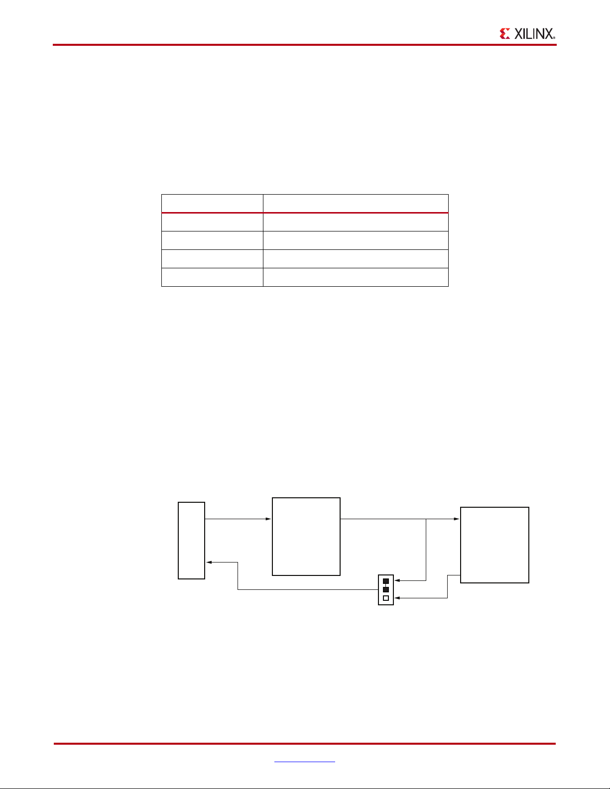
JTAG Configuration
JTAG configuration is provided through onboard USB-to-JTAG configuration logic where
a computer host accesses the SP601 JTAG chain through a Type-A (computer host side) to
Type-Mini-B (SP601 side) USB cable.
The JTAG chain of the board is illustrated in Figure 1-16. JTAG configuration is allowable
at any time under any mode pin setting. JTAG initiated configuration takes priority over
the mode pin settings.
FMC bypass jumper J4 must be connected between pins 1-2 for JTAG access to the FPGA
on the basic SP601 board, as shown in Figure 1-16. When the VITA 57.1 FMC expansion
connector is populated with an expansion module that has a JTAG chain, then jumper J4
must be set to connect pins 2-3 in order to include the FMC expansion module's JTAG
chain in the main SP601 JTAG chain.
X-Ref Target - Figure 1-16
TDI
FPGA
U1
TDO
FMC LPC Expansion
TDI
J4
1
*Default jumper setting excludes FMC.
To include FMC, jumper pins 2-3.
TDO
J1
UG518_31_070809
J10
Connector
USB Mini-B
Figure 1-16: JTAG Chain
36 www.xilinx.com SP601 Hardware User Guide
UG518 (v1.7) September 26, 2012
Page 37
X-Ref Target - Figure 1-17
Bypass FMC LPC J1 = Jumper 1–2
Include FMC LPC J1 = Jumper 2–3
J4
Detailed Description
1
2
3
FPGA_TD0
JTAG_TD0
FMC_TD0
Figure 1-17: VITA 57.1 FMC JTAG Bypass Jumper
The JTAG chain can be used to program the FPGA and access the FPGA for hardware and
software debug.
The JTAG connector (USB Mini-B J10) allows a host computer to download bitstreams to
the FPGA using the iMPACT software tool, and also allows debug tools such as the
ChipScope™ Pro Analyzer tool or a software debugger to access the FPGA.
The iMPACT software tool can also program the SPI x4 flash or the BPI flash via the USB
J10 connection. iMPACT can download a temporary design to the FPGA through the JTAG.
This provides a connection within the FPGA from the FPGA's JTAG port to the FPGA's SPI
or BPI interface. Through the connection made by the temporary design in the FPGA,
iMPACT can indirectly program the SPI flash or BPI flash from the JTAG USB J10
connector.
16. Power Management
AC Adapter and 5V Input Power Jack/Switch
The SP601 is powered from a 5V source that is connected through a 2.1 mm x 5.5 mm type
plug (center positive).
switch. When the switch is in the on position, a green LED (DS15) is illuminated.
H - 1x3
SP601 power can be turned on or off through a board mounted slide
UG518_32_040910
Onboard Power Supplies
The diagram in Figure 1-18 shows the power supply architecture and maximum current
handling on each supply. The typical operating currents are significantly below the
maximum capable. The board is normally shipped with a 15W power supply, which
should be sufficient for most applications. The
Technology Corporation (LTC).
SP601 Hardware User Guide www.xilinx.com 37
UG518 (v1.7) September 26, 2012
SP601 uses power solutions from Linear
Page 38
Chapter 1: SP601 Evaluation Board
Power System Test Points
The SP601 has 17 Keystone 5002 miniature PC test points, TP1 to TP17. These test points
are identified in the SP601 board schematic, and the function of each is listed in Tab le 1- 25 .
Table 1-25: SP601 Power System Test Points
REFDES Function
TP1 5.0V Input Voltage
TP2 GND
TP3 2.5V VCCO and Logic
TP4 3.3V FMC and Logic
TP5 LTM4616 U15 ITH pin M8 for 2.5V regulator
TP6 LTM4616 U15 ITH pin F8 for 3.3V regulator
TP7 1.2V VCCINT
TP8 1.8V DDR2
TP9 LTM4616 U19 ITH pin M8 for 1.2V regulator
TP10 LTM4616 U19 ITH pin F8 for 1.8V regulator
TP11 0.9V VTT_DDR2 memory termination voltage
TP12 12V FMC
TP13 3.0V J3D U10 Flash
TP14 GND
TP15 GND
TP16 GND
TP17 GND
38 www.xilinx.com SP601 Hardware User Guide
UG518 (v1.7) September 26, 2012
Page 39

X-Ref Target - Figure 1-18
5V
PWR
Jack
J18
Dual Switcher LTM4616 U15
DDR2 Memory Termination
System, FMC Connector
FPGA VCCAUX, VCCO
FMC VADJ, System
FPGA
VTT_DDR2
VCC3V3
VCC2V5
VCCINT
VCC1V8
VCC3V0
VCC12VP
DDR2 Memory
SPI x4 Memory
BPI Memory
FMC Connector
3. 3V@8A max
2. 5V@8A max
Dual Switcher LTM4616 U19
1. 2V@8A max
1. 8V@8A max
Linear Regulator LT1763 U11
Linear Regulator U18
LTC3413 0.9V@3A max
Buck-Boost Regulator LT1731
12V@1A max U8
3. 0V@500mA max
UG518_03_060210
Detailed Description
Figure 1-18: Power Supply
Table 1-26: Onboard Power System Devices
Device Type
Reference
Designator
Description
LTM4616IV#PBF U19 1/2 Dual 8A Switching uModule VCCINT
Power Rail Net
Name
(1)
Power Rail
Voltag e (V )
1.20 12
LTM4616IV#PBF U19 1/2 Dual 8A Switching uModule VCC1V8 1.80 12
LTM4616IV#PBF U15 1/2 Dual 8A Switching uModule VCC2V5 2.50 11
LTM4616IV#PBF U15 1/2 Dual 8A Switching uModule VCC3V3 3.30 11
LTC3413EFE#PBF U18 3A Memory Term. Switching
VTT_DDR2 0.9 13
Regulator
LTC1763CS8#TRPBF U11 500 mA LDO Linear Regulator VCC3V0 3.0 13
LT1371CR#TRPBF U8 3A Switching Regulator VCC12V_P 12 13
Notes:
1. V
tolerance meets or exceeds the V
CCINT
Spartan-6 FPGA Data Sheet. [Ref 1]
±5% specification in the Recommended Operating Conditions table in the
CCINT
Schematic
Page
SP601 Hardware User Guide www.xilinx.com 39
UG518 (v1.7) September 26, 2012
Page 40

Chapter 1: SP601 Evaluation Board
40 www.xilinx.com SP601 Hardware User Guide
UG518 (v1.7) September 26, 2012
Page 41

Appendix A
Default Jumper and Switch Settings
Tab le A -1 shows the default jumper and switch settings for the SP601.
Tab le A- 1 : Default Jumper and Switch Settings
REFDES Type/Function Default
SW1 SLIDE, POWER ON-OFF OFF
SW2 DIP, 2-POLE, MODE
1M0 ON (1)
2 M1 OFF (0)
SW8 DIP, 4-POLE, GPIO
1OFF
2OFF
3OFF
4OFF
J4 HDR_1X3, JTAG BYPASS JUMP 1-2 (EXCLUDE FMC)
J14 HDR_1X2, SUSPEND OPEN (0 = AWAKE)
J15 HDR_1X2, SPI SELECT ON (U17 SPI MEM SELECTED)
SP601 Hardware User Guide www.xilinx.com 41
UG518 (v1.7) September 26, 2012
Page 42

Appendix A: Default Jumper and Switch Settings
42 www.xilinx.com SP601 Hardware User Guide
UG518 (v1.7) September 26, 2012
Page 43

Appendix B
VITA 57.1 FMC LPC Connector Pinout
Figure B-1 shows the pinout of the FMC LPC connector. Pins marked NC are not
connected.
X-Ref Target - Figure B-1
KJ H G FE D C BA
1 NC NC VR EF_A_M2C GND NC NC PG_C2M G ND NC NC
2 NC NC PR SNT_M2C_L C LK 1_M2C_P NC NC GND DP 0_C2M_P N C NC
3 NC NC GND C LK 1_M2C_N NC NC GND DP 0_C2M_N NC NC
4 NC NC CLK0_M2C _P GND NC NC GBT CLK0_M2C _P GND NC NC
5 NC NC CL K0_M2C _N GND NC NC GBT CLK0_M2C_N GND NC NC
6 NC NC GN D L A0 0 _P _C C N C N C G ND DP 0_ M 2 C_ P N C N C
7 NC NC LA02_P LA00_N_C C NC NC G ND DP0_M2C_N NC NC
8 NC NC LA02_N GND NC NC LA01_P_C C GND NC NC
9 NC N C GN D L A0 3 _P NC N C LA0 1 _N _C C G ND NC N C
10 NC NC LA04_P LA03_N NC NC GND LA06_P NC NC
11 NC NC LA04_N GND NC NC LA05_P LA06_N NC NC
12 NC NC G ND LA08_P NC NC LA05_N GND NC NC
13 NC NC LA07_P LA08_N NC NC GN D G ND NC NC
14 NC NC LA07_N GND NC NC LA09_P LA10_P NC NC
15 NC NC G ND LA12_P NC NC LA0 9 _N LA1 0 _N NC NC
16 NC NC LA11_P LA12_N NC NC GN D G ND NC NC
17 NC NC LA11_N GND NC NC LA13_P GND NC NC
18 NC NC G ND LA16_P NC NC LA13_N LA14_P NC NC
19 NC NC LA15_P LA16_N NC NC GN D LA14_N NC NC
20 NC NC LA15_N GND NC NC L A17_P _C C GND NC NC
21 NC NC G ND LA20_P NC NC LA17_N_CC GND NC NC
22 NC NC LA19_P LA20_N NC NC GN D LA18_P _C C N C NC
23 NC NC LA19_N GND NC NC LA23_P LA18_N_C C NC NC
24 NC NC G ND LA22_P NC NC LA23_N GND NC NC
25 NC NC LA21_P LA22_N NC NC GN D G ND NC NC
26 NC NC LA21_N GND NC NC LA26_P LA27_P NC NC
27 NC NC G ND LA25_P NC NC LA2 6 _N LA2 7 _N NC NC
28 NC NC LA24_P LA25_N NC NC GN D G ND NC NC
29 NC NC LA24_N GND NC NC TCK GND NC NC
30 NC NC G ND LA29_P NC NC TDI S CL NC NC
31 NC NC LA28_P LA29_N NC NC TDO S DA NC NC
32 NC NC LA28_N GND NC NC 3P3VAUX GND NC NC
33 NC NC G ND LA31_P NC NC TMS GND NC NC
34 NC NC LA30_P LA31_N NC NC TR ST _L GA0 NC NC
35 NC NC LA30_N GND NC NC GA1 12P0V NC NC
36 NC NC G ND LA33_P NC NC 3P 3V GND NC NC
37 NC NC L A32_P LA33_N NC NC GND 12P0V NC NC
38 NC NC LA32_N GND NC NC 3P3V G ND NC NC
39 NC NC G ND VADJ NC NC GND 3P3V NC NC
40 NC NC VADJ GND NC NC 3P 3V GND NC NC
Figure B-1: FMC LPC Connector Pinout
For more information, refer to the VITA 57.1 FMC LPC Connections table (Ta b le 1 -1 4).
SP601 Hardware User Guide www.xilinx.com 43
UG518 (v1.7) September 26, 2012
Page 44

Appendix B: VITA 57.1 FMC LPC Connector Pinout
44 www.xilinx.com SP601 Hardware User Guide
UG518 (v1.7) September 26, 2012
Page 45

SP601 Master UCF
The UCF template is provided for designs that target the SP601. Net names provided in the
constraints below correlate with net names on the SP601 schematic. On identifying the
appropriate pins, the net names below should be replaced with net names in the user RTL.
See the Constraints Guide
The latest version of the UCF can be found on the SP601 board documentation website at
http://www.xilinx.com/sp601
NET "CPU_RESET" LOC = "N4"; ## 2 on SW9 pushbutton
##
NET "DDR2_A0" LOC = "J7"; | IOSTANDARD = SSTL18_II ; ## M8 on U2
NET "DDR2_A1" LOC = "J6"; | IOSTANDARD = SSTL18_II ; ## M3 on U2
NET "DDR2_A2" LOC = "H5"; | IOSTANDARD = SSTL18_II ; ## M7 on U2
NET "DDR2_A3" LOC = "L7"; | IOSTANDARD = SSTL18_II ; ## N2 on U2
NET "DDR2_A4" LOC = "F3"; | IOSTANDARD = SSTL18_II ; ## N8 on U2
NET "DDR2_A5" LOC = "H4"; | IOSTANDARD = SSTL18_II ; ## N3 on U2
NET "DDR2_A6" LOC = "H3"; | IOSTANDARD = SSTL18_II ; ## N7 on U2
NET "DDR2_A7" LOC = "H6"; | IOSTANDARD = SSTL18_II ; ## P2 on U2
NET "DDR2_A8" LOC = "D2"; | IOSTANDARD = SSTL18_II ; ## P8 on U2
NET "DDR2_A9" LOC = "D1"; | IOSTANDARD = SSTL18_II ; ## P3 on U2
NET "DDR2_A10" LOC = "F4"; | IOSTANDARD = SSTL18_II ; ## M2 on U2
NET "DDR2_A11" LOC = "D3"; | IOSTANDARD = SSTL18_II ; ## P7 on U2
NET "DDR2_A12" LOC = "G6"; | IOSTANDARD = SSTL18_II ; ## R2 on U2
NET "DDR2_BA0" LOC = "F2"; | IOSTANDARD = SSTL18_II ; ## L2 on U2
NET "DDR2_BA1" LOC = "F1"; | IOSTANDARD = SSTL18_II ; ## L3 on U2
NET "DDR2_BA2" LOC = "E1"; | IOSTANDARD = SSTL18_II ; ## L1 on U2
NET "DDR2_CAS_B" LOC = "K5"; | IOSTANDARD = SSTL18_II ; ## L7 on U2
NET "DDR2_CKE" LOC = "H7"; | IOSTANDARD = SSTL18_II ; ## K2 on U2
NET "DDR2_CLK_N" LOC = "G1"; | IOSTANDARD = SSTL18_II ; ## K8 on U2
NET "DDR2_CLK_P" LOC = "G3"; | IOSTANDARD = SSTL18_II ; ## J8 on U2
NET "DDR2_DQ0" LOC = "L2"; | IOSTANDARD = SSTL18_II ; ## G8 on U2
NET "DDR2_DQ1" LOC = "L1"; | IOSTANDARD = SSTL18_II ; ## G2 on U2
NET "DDR2_DQ2" LOC = "K2"; | IOSTANDARD = SSTL18_II ; ## H7 on U2
NET "DDR2_DQ3" LOC = "K1"; | IOSTANDARD = SSTL18_II ; ## H3 on U2
NET "DDR2_DQ4" LOC = "H2"; | IOSTANDARD = SSTL18_II ; ## H1 on U2
NET "DDR2_DQ5" LOC = "H1"; | IOSTANDARD = SSTL18_II ; ## H9 on U2
NET "DDR2_DQ6" LOC = "J3"; | IOSTANDARD = SSTL18_II ; ## F1 on U2
NET "DDR2_DQ7" LOC = "J1"; | IOSTANDARD = SSTL18_II ; ## F9 on U2
NET "DDR2_DQ8" LOC = "M3"; | IOSTANDARD = SSTL18_II ; ## C8 on U2
NET "DDR2_DQ9" LOC = "M1"; | IOSTANDARD = SSTL18_II ; ## C2 on U2
NET "DDR2_DQ10" LOC = "N2"; | IOSTANDARD = SSTL18_II ; ## D7 on U2
NET "DDR2_DQ11" LOC = "N1"; | IOSTANDARD = SSTL18_II ; ## D3 on U2
NET "DDR2_DQ12" LOC = "T2"; | IOSTANDARD = SSTL18_II ; ## D1 on U2
NET "DDR2_DQ13" LOC = "T1"; | IOSTANDARD = SSTL18_II ; ## D9 on U2
NET "DDR2_DQ14" LOC = "U2"; | IOSTANDARD = SSTL18_II ; ## B1 on U2
NET "DDR2_DQ15" LOC = "U1"; | IOSTANDARD = SSTL18_II ; ## B9 on U2
NET "DDR2_LDM" LOC = "K3"; | IOSTANDARD = SSTL18_II ; ## F3 on U2
NET "DDR2_LDQS_N" LOC = "L3"; | IOSTANDARD = SSTL18_II ; ## E8 on U2
NET "DDR2_LDQS_P" LOC = "L4"; | IOSTANDARD = SSTL18_II ; ## F7 on U2
for more information.
.
Appendix C
SP601 Hardware User Guide www.xilinx.com 45
UG518 (v1.7) September 26, 2012
Page 46

Appendix C: SP601 Master UCF
NET "DDR2_ODT" LOC = "K6"; | IOSTANDARD = SSTL18_II ; ## K9 on U2
NET "DDR2_RAS_B" LOC = "L5"; | IOSTANDARD = SSTL18_II ; ## K7 on U2
NET "DDR2_UDM" LOC = "K4"; | IOSTANDARD = SSTL18_II ; ## B3 on U2
NET "DDR2_UDQS_N" LOC = "P1"; | IOSTANDARD = SSTL18_II ; ## A8 on U2
NET "DDR2_UDQS_P" LOC = "P2"; | IOSTANDARD = SSTL18_II ; ## B7 on U2
NET "DDR2_WE_B" LOC = "E3"; | IOSTANDARD = SSTL18_II ; ## K3 on U2
##
NET "FLASH_A0" LOC = "K18"; ## 32 on U10
NET "FLASH_A1" LOC = "K17"; ## 28 on U10
NET "FLASH_A2" LOC = "J18"; ## 27 on U10
NET "FLASH_A3" LOC = "J16"; ## 26 on U10
NET "FLASH_A4" LOC = "G18"; ## 25 on U10
NET "FLASH_A5" LOC = "G16"; ## 24 on U10
NET "FLASH_A6" LOC = "H16"; ## 23 on U10
NET "FLASH_A7" LOC = "H15"; ## 22 on U10
NET "FLASH_A8" LOC = "H14"; ## 20 on U10
NET "FLASH_A9" LOC = "H13"; ## 19 on U10
NET "FLASH_A10" LOC = "F18"; ## 18 on U10
NET "FLASH_A11" LOC = "F17"; ## 17 on U10
NET "FLASH_A12" LOC = "K13"; ## 13 on U10
NET "FLASH_A13" LOC = "K12"; ## 12 on U10
NET "FLASH_A14" LOC = "E18"; ## 11 on U10
NET "FLASH_A15" LOC = "E16"; ## 10 on U10
NET "FLASH_A16" LOC = "G13"; ## 8 on U10
NET "FLASH_A17" LOC = "H12"; ## 7 on U10
NET "FLASH_A18" LOC = "D18"; ## 6 on U10
NET "FLASH_A19" LOC = "D17"; ## 5 on U10
NET "FLASH_A20" LOC = "G14"; ## 4 on U10
NET "FLASH_A21" LOC = "F14"; ## 3 on U10
NET "FLASH_A22" LOC = "C18"; ## 1 on U10
NET "FLASH_A23" LOC = "C17"; ## 30 on U10
NET "FLASH_A24" LOC = "F16"; ## 56 on U10
NET "FLASH_CE_B" LOC = "L17"; ## 14 on U10
NET "FLASH_D3" LOC = "U5"; ## 40 on U10
NET "FLASH_D4" LOC = "V5"; ## 44 on U10
NET "FLASH_D5" LOC = "R3"; ## 46 on U10
NET "FLASH_D6" LOC = "T3"; ## 49 on U10
NET "FLASH_D7" LOC = "R5"; ## 51 on U10
NET "FLASH_OE_B" LOC = "L18"; ## 54 on U10
NET "FLASH_WE_B" LOC = "M16"; ## 55 on U10
##
NET "FMC_CLK0_M2C_N" LOC = "A10"; ## H5 on J1
NET "FMC_CLK0_M2C_P" LOC = "C10"; ## H4 on J1
NET "FMC_CLK1_M2C_N" LOC = "V9"; ## G3 on J1
NET "FMC_CLK1_M2C_P" LOC = "T9"; ## G2 on J1
NET "FMC_LA00_CC_N" LOC = "C9"; ## G7 on J1
NET "FMC_LA00_CC_P" LOC = "D9"; ## G6 on J1
NET "FMC_LA01_CC_N" LOC = "C11"; ## D9 on J1
NET "FMC_LA01_CC_P" LOC = "D11"; ## D8 on J1
NET "FMC_LA02_N" LOC = "A15"; ## H8 on J1
NET "FMC_LA02_P" LOC = "C15"; ## H7 on J1
NET "FMC_LA03_N" LOC = "A13"; ## G10 on J1
NET "FMC_LA03_P" LOC = "C13"; ## G9 on J1
NET "FMC_LA04_N" LOC = "A16"; ## H11 on J1
NET "FMC_LA04_P" LOC = "B16"; ## H10 on J1
NET "FMC_LA05_N" LOC = "A14"; ## D12 on J1
NET "FMC_LA05_P" LOC = "B14"; ## D11 on J1
NET "FMC_LA06_N" LOC = "C12"; ## C11 on J1
NET "FMC_LA06_P" LOC = "D12"; ## C10 on J1
NET "FMC_LA07_N" LOC = "E8"; ## H14 on J1
NET "FMC_LA07_P" LOC = "E7"; ## H13 on J1
NET "FMC_LA08_N" LOC = "E11"; ## G13 on J1
NET "FMC_LA08_P" LOC = "F11"; ## G12 on J1
NET "FMC_LA09_N" LOC = "F10"; ## D15 on J1
NET "FMC_LA09_P" LOC = "G11"; ## D14 on J1
46 www.xilinx.com SP601 Hardware User Guide
UG518 (v1.7) September 26, 2012
Page 47

NET "FMC_LA10_N" LOC = "C8"; ## C15 on J1
NET "FMC_LA10_P" LOC = "D8"; ## C14 on J1
NET "FMC_LA11_N" LOC = "A12"; ## H17 on J1
NET "FMC_LA11_P" LOC = "B12"; ## H16 on J1
NET "FMC_LA12_N" LOC = "C6"; ## G16 on J1
NET "FMC_LA12_P" LOC = "D6"; ## G15 on J1
NET "FMC_LA13_N" LOC = "A11"; ## D18 on J1
NET "FMC_LA13_P" LOC = "B11"; ## D17 on J1
NET "FMC_LA14_N" LOC = "A2"; ## C19 on J1
NET "FMC_LA14_P" LOC = "B2"; ## C18 on J1
NET "FMC_LA15_N" LOC = "F9"; ## H20 on J1
NET "FMC_LA15_P" LOC = "G9"; ## H19 on J1
NET "FMC_LA16_N" LOC = "A7"; ## G19 on J1
NET "FMC_LA16_P" LOC = "C7"; ## G18 on J1
NET "FMC_LA17_CC_N" LOC = "T8"; ## D21 on J1
NET "FMC_LA17_CC_P" LOC = "R8"; ## D20 on J1
NET "FMC_LA18_CC_N" LOC = "T10"; ## C23 on J1
NET "FMC_LA18_CC_P" LOC = "R10"; ## C22 on J1
NET "FMC_LA19_N" LOC = "P7"; ## H23 on J1
NET "FMC_LA19_P" LOC = "N6"; ## H22 on J1
NET "FMC_LA20_N" LOC = "P8"; ## G22 on J1
NET "FMC_LA20_P" LOC = "N7"; ## G21 on J1
NET "FMC_LA21_N" LOC = "V4"; ## H26 on J1
NET "FMC_LA21_P" LOC = "T4"; ## H25 on J1
NET "FMC_LA22_N" LOC = "T7"; ## G25 on J1
NET "FMC_LA22_P" LOC = "R7"; ## G24 on J1
NET "FMC_LA23_N" LOC = "P6"; ## D24 on J1
NET "FMC_LA23_P" LOC = "N5"; ## D23 on J1
NET "FMC_LA24_N" LOC = "V8"; ## H29 on J1
NET "FMC_LA24_P" LOC = "U8"; ## H28 on J1
NET "FMC_LA25_N" LOC = "N11"; ## G28 on J1
NET "FMC_LA25_P" LOC = "M11"; ## G27 on J1
NET "FMC_LA26_N" LOC = "V7"; ## D27 on J1
NET "FMC_LA26_P" LOC = "U7"; ## D26 on J1
NET "FMC_LA27_N" LOC = "T11"; ## C27 on J1
NET "FMC_LA27_P" LOC = "R11"; ## C26 on J1
NET "FMC_LA28_N" LOC = "V11"; ## H32 on J1
NET "FMC_LA28_P" LOC = "U11"; ## H31 on J1
NET "FMC_LA29_N" LOC = "N8"; ## G31 on J1
NET "FMC_LA29_P" LOC = "M8"; ## G30 on J1
NET "FMC_LA30_N" LOC = "V12"; ## H35 on J1
NET "FMC_LA30_P" LOC = "T12"; ## H34 on J1
NET "FMC_LA31_N" LOC = "V6"; ## G34 on J1
NET "FMC_LA31_P" LOC = "T6"; ## G33 on J1
NET "FMC_LA32_N" LOC = "V15"; ## H38 on J1
NET "FMC_LA32_P" LOC = "U15"; ## H37 on J1
NET "FMC_LA33_N" LOC = "N9"; ## G37 on J1
NET "FMC_LA33_P" LOC = "M10"; ## G36 on J1
NET "FMC_PRSNT_M2C_L" LOC = "U13"; ## H2 on J1
NET "FMC_PWR_GOOD_FLASH_RST_B" LOC = "B3"; ## D1 on J1, 16 on U10
##
NET "FPGA_AWAKE" LOC = "P15"; ## 2 on DS8 LED
NET "FPGA_CCLK" LOC = "R15"; ## 16 on U17, 7 on J12
NET "FPGA_CMP_CLK" LOC = "U16"; ## 3 on J3
NET "FPGA_CMP_CS_B" LOC = "P13"; ## 4 on J3
NET "FPGA_CMP_MOSI" LOC = "V16"; ## 2 on J3
NET "FPGA_D0_DIN_MISO_MISO1" LOC = "R13"; ## 8 on U17 (thru series R187 100 ohm), 33 on U10, 6 on J12
NET "FPGA_D1_MISO2" LOC = "T14"; ## 9 on U17 (thru series R186 100 ohm), 35 on U10, 3 on J12
NET "FPGA_D2_MISO3" LOC = "V14"; ## 1 on U17, 38 on U10, 2 on J12
NET "FPGA_DONE" LOC = "V17"; ## 2 on DS9 LED
NET "FPGA_HSWAPEN" LOC = "D4"; ## 1 on R81 100 ohm to GND
NET "FPGA_INIT_B" LOC = "U3"; ## 1 on DS10 (thru series R90 27.4 ohm)
NET "FPGA_M0_CMP_MISO" LOC = "T15"; ## 1 on J3, 1 on SW2 DIP Sw
NET "FPGA_M1" LOC = "N12"; ## 2 on SW2 DIP Sw
NET "FPGA_MOSI_CSI_B_MISO0" LOC = "T13"; ## 15 on U17, 5 on J12
SP601 Hardware User Guide www.xilinx.com 47
UG518 (v1.7) September 26, 2012
Page 48

Appendix C: SP601 Master UCF
NET "FPGA_ONCHIP_TERM1" LOC = "L6"; ## ZIO no connect (R86 is DNP)
NET "FPGA_ONCHIP_TERM2" LOC = "C2"; ## RZQ 100 ohm to GND
NET "FPGA_PROG_B" LOC = "V2"; ## 1 on SW3 pushbutton
NET "FPGA_SUSPEND" LOC = "R16"; ## 2 on J14
NET "FPGA_TCK_BUF" LOC = "A17"; ## 14 on U21, D29 on J1
NET "FPGA_TDI_BUF" LOC = "D15"; ## 18 on U21
NET "FPGA_TDO" LOC = "D16"; ## 1 on J4, D30 on J1
NET "FPGA_TMS_BUF" LOC = "B18"; ## 16 on U21, D31 on J1
NET "FPGA_VTEMP" LOC = "P3"; ## 2 on R87 150 ohm p/u to VCC1V8
##
NET "GPIO_BUTTON0" LOC = "P4"; ## 2 on SW6 pushbutton
NET "GPIO_BUTTON1" LOC = "F6"; ## 2 on SW4 pushbutton
NET "GPIO_BUTTON2" LOC = "E4"; ## 2 on SW5 pushbutton
NET "GPIO_BUTTON3" LOC = "F5"; ## 2 on SW7 pushbutton
##
NET "GPIO_HDR0" LOC = "N17"; ## 1 on J13 (thru series R100 200 ohm)
NET "GPIO_HDR1" LOC = "M18"; ## 3 on J13 (thru series R102 200 ohm)
NET "GPIO_HDR2" LOC = "A3"; ## 5 on J13 (thru series R101 200 ohm)
NET "GPIO_HDR3" LOC = "L15"; ## 7 on J13 (thru series R103 200 ohm)
NET "GPIO_HDR4" LOC = "F15"; ## 2 on J13 (thru series R99 200 ohm)
NET "GPIO_HDR5" LOC = "B4"; ## 4 on J13 (thru series R98 200 ohm)
NET "GPIO_HDR6" LOC = "F13"; ## 6 on J13 (thru series R97 200 ohm)
NET "GPIO_HDR7" LOC = "P12"; ## 8 on J13 (thru series R96 200 ohm)
##
NET "GPIO_LED_0" LOC = "E13"; ## 2 on DS11 LED
NET "GPIO_LED_1" LOC = "C14"; ## 2 on DS12 LED
NET "GPIO_LED_2" LOC = "C4"; ## 2 on DS13 LED
NET "GPIO_LED_3" LOC = "A4"; ## 2 on DS14 LED
##
NET "GPIO_SWITCH_0" LOC = "D14"; ## 1 on SW8 DIP Sw
NET "GPIO_SWITCH_1" LOC = "E12"; ## 2 on SW8 DIP Sw
NET "GPIO_SWITCH_2" LOC = "F12"; ## 3 on SW8 DIP Sw
NET "GPIO_SWITCH_3" LOC = "V13"; ## 4 on SW8 DIP Sw
##
NET "IIC_SCL_MAIN" LOC = "P11"; ## 6 on U7 (thru series R203 0 ohm), C30 on J1, 2 on J16
NET "IIC_SDA_MAIN" LOC = "N10"; ## 5 on U7 (thru series R204 0 ohm), C31 on J1, 1 on J16
##
NET "PHY_COL" LOC = "L14"; ## 114 on U3
NET "PHY_CRS" LOC = "M13"; ## 115 on U3
NET "PHY_INT" LOC = "J13"; ## 32 on U3
NET "PHY_MDC" LOC = "N14"; ## 35 on U3
NET "PHY_MDIO" LOC = "P16"; ## 33 on U3
NET "PHY_RESET" LOC = "L13"; ## 36 on U3
NET "PHY_RXCLK" LOC = "L16"; ## 7 on U3
NET "PHY_RXCTL_RXDV" LOC = "N18"; ## 4 on U3
NET "PHY_RXD0" LOC = "M14"; ## 3 on U3
NET "PHY_RXD1" LOC = "U18"; ## 128 on U3
NET "PHY_RXD2" LOC = "U17"; ## 126 on U3
NET "PHY_RXD3" LOC = "T18"; ## 125 on U3
NET "PHY_RXD4" LOC = "T17"; ## 124 on U3
NET "PHY_RXD5" LOC = "N16"; ## 123 on U3
NET "PHY_RXD6" LOC = "N15"; ## 121 on U3
NET "PHY_RXD7" LOC = "P18"; ## 120 on U3
NET "PHY_RXER" LOC = "P17"; ## 8 on U3
NET "PHY_TXCLK" LOC = "B9"; ## 10 on U3
NET "PHY_TXCTL_TXEN" LOC = "B8"; ## 16 on U3
NET "PHY_TXC_GTXCLK" LOC = "A9"; ## 14 on U3
NET "PHY_TXD0" LOC = "F8"; ## 18 on U3
NET "PHY_TXD1" LOC = "G8"; ## 19 on U3
NET "PHY_TXD2" LOC = "A6"; ## 20 on U3
NET "PHY_TXD3" LOC = "B6"; ## 24 on U3
NET "PHY_TXD4" LOC = "E6"; ## 25 on U3
NET "PHY_TXD5" LOC = "F7"; ## 26 on U3
NET "PHY_TXD6" LOC = "A5"; ## 28 on U3
NET "PHY_TXD7" LOC = "C5"; ## 29 on U3
48 www.xilinx.com SP601 Hardware User Guide
UG518 (v1.7) September 26, 2012
Page 49

NET "PHY_TXER" LOC = "A8"; ## 13 on U3
##
NET "SMACLK_N" LOC = "H18"; ## 1 on J8 SMA
NET "SMACLK_P" LOC = "H17"; ## 1 on J7 SMA
##
NET "SPI_CS_B" LOC = "V3"; ## 1 on J15, 4 on J12
##
NET "SYSCLK_N" LOC = "K16"; ## 5 on U5 EG2121CA, 5 of U20 SI500D (DNP)
NET "SYSCLK_P" LOC = "K15"; ## 6 on U5 EG2121CA, 4 of U20 SI500D (DNP)
##
NET "USB_1_CTS" LOC = "U10"; ## 22 on U4
NET "USB_1_RTS" LOC = "T5"; ## 23 on U4
NET "USB_1_RX" LOC = "L12"; ## 24 on U4
NET "USB_1_TX" LOC = "K14"; ## 25 on U4
##
NET "USER_CLOCK" LOC = "V10"; ## 5 on X2 USER OSC Socket
SP601 Hardware User Guide www.xilinx.com 49
UG518 (v1.7) September 26, 2012
Page 50

Appendix C: SP601 Master UCF
50 www.xilinx.com SP601 Hardware User Guide
UG518 (v1.7) September 26, 2012
Page 51

References
This section provides references to documentation supporting Spartan-6 FPGAs, tools, and
IP. For additional information, see www.xilinx.com/support/documentation/index.htm
Documents supporting the SP601 Evaluation Board:
1. DS162, Spartan-6 FPGA Data Sheet: DC and Switching Characteristics
2. UG380
3. UG388
4. DS570
5. UG138
6. DS606
7. U
8. DS614
9. DS643
10. UG394
Appendix D
.
, Spartan-6 FPGA Configuration User Guide
, Spartan-6 FPGA Memory Controller User Guide
, XPS Serial Peripheral Interface (SPI) Data Sheet
, LogiCORE™ IP Tri-Mode Ethernet MAC v4.2 User Guide
, XPS IIC Bus Interface (v2.00a) Data Sheet
G381, Spartan-6 FPGA SelectIO Resources User Guide
, Clock Generator (v3.01a) Data Sheet
, Multi-Port Memory Controller (MPMC) (v5.02a) Data Sheet
, Spartan-6 FPGA Power Management User Guide
Additional documentation:
11. Elpida, DDR2 SDRAM Specifications (EDE1116ACBG)
12. Winbond , Serial Flash Memory Data Sheet (W25Q64VSFIG)
13. Numonyx, Embedded Flash Memory Data Sheet (TE28F128J3D-75)
14. SiTime
15. PCI SIG
16. Marvell
17. ST Micro
, Oscillator Data Sheet (SiT9102AI-243N25E200.00000)
, PCI Express Specifications
, Alaska Gigabit Ethernet Transceivers Product Page
, M24C08 Data Sheet
SP601 Hardware User Guide www.xilinx.com 51
UG518 (v1.7) September 26, 2012
Page 52

Appendix D: References
52 www.xilinx.com SP601 Hardware User Guide
UG518 (v1.7) September 26, 2012
Page 53

Regulatory and Compliance Information
This product is designed and tested to conform to the European Union directives and
standards described in this section.
Directives
2006/95/EC, Low Voltage Directive (LVD)
2004/108/EC, Electromagnetic Compatibility (EMC) Directive
Standards
Appendix E
EN standards are maintained by the European Committee for Electrotechnical
Standardization (CENELEC). IEC standards are maintained by the International
Electrotechnical Commission (IEC).
Electromagnetic Compatibility
EN 55022:2010, Information Technology Equipment Radio Disturbance Characteristics – Limits
and Methods of Measurement
EN 55024:2010, Information Technology Equipment Immunity Characteristics – Limits and
Methods of Measurement
This is a Class A product. In a domestic environment, this product can cause radio
interference, in which case the user might be required to take adequate measures.
Safety
IEC 60950-1:2005, Information technology equipment – Safety, Part 1: General requirements
EN 60950-1:2006, Information technology equipment – Safety, Part 1: General requirements
SP601 Hardware User Guide www.xilinx.com 53
UG518 (v1.7) September 26, 2012
Page 54

Appendix E: Regulatory and Compliance Information
Markings
This product complies with Directive 2002/96/EC on waste electrical and electronic
equipment (WEEE). The affixed product label indicates that the user must not discard this
electrical or electronic product in domestic household waste.
This product complies with Directive 2002/95/EC on the restriction of hazardous substances
(RoHS) in electrical and electronic equipment.
This product complies with CE Directives 2006/95/EC, Low Voltage Directive (LVD) and
2004/108/EC, Electromagnetic Compatibility (EMC) Directive.
54 www.xilinx.com SP601 Hardware User Guide
UG518 (v1.7) September 26, 2012
 Loading...